US5200979A - High speed telecommunication system using a novel line code - Google Patents
High speed telecommunication system using a novel line code Download PDFInfo
- Publication number
- US5200979A US5200979A US07/710,995 US71099591A US5200979A US 5200979 A US5200979 A US 5200979A US 71099591 A US71099591 A US 71099591A US 5200979 A US5200979 A US 5200979A
- Authority
- US
- United States
- Prior art keywords
- bits
- bit
- balance
- data
- frame
- Prior art date
- Legal status (The legal status is an assumption and is not a legal conclusion. Google has not performed a legal analysis and makes no representation as to the accuracy of the status listed.)
- Expired - Lifetime
Links
Images


Classifications
-
- H—ELECTRICITY
- H04—ELECTRIC COMMUNICATION TECHNIQUE
- H04L—TRANSMISSION OF DIGITAL INFORMATION, e.g. TELEGRAPHIC COMMUNICATION
- H04L25/00—Baseband systems
- H04L25/38—Synchronous or start-stop systems, e.g. for Baudot code
- H04L25/40—Transmitting circuits; Receiving circuits
- H04L25/49—Transmitting circuits; Receiving circuits using code conversion at the transmitter; using predistortion; using insertion of idle bits for obtaining a desired frequency spectrum; using three or more amplitude levels ; Baseband coding techniques specific to data transmission systems
- H04L25/4906—Transmitting circuits; Receiving circuits using code conversion at the transmitter; using predistortion; using insertion of idle bits for obtaining a desired frequency spectrum; using three or more amplitude levels ; Baseband coding techniques specific to data transmission systems using binary codes
- H04L25/4915—Transmitting circuits; Receiving circuits using code conversion at the transmitter; using predistortion; using insertion of idle bits for obtaining a desired frequency spectrum; using three or more amplitude levels ; Baseband coding techniques specific to data transmission systems using binary codes using pattern inversion or substitution
Definitions
- the present invention relates generally to a high speed digital telecommunication technique.
- it is directed to a method of and an apparatus for communicating serially at high speed digital data signals which are block-coded in a new and more efficient format for a good statistically balanced transmission.
- raw data is modulated (encoded, or simply coded) into PCM signals and then are transmitted to a destination terminal or terminals.
- the received PCM signals are then demodulated (decoded) into the identical raw data at the destination.
- coding coding
- decoding schemes also called formats.
- a specific coding scheme (or format) is chosen for a particular application, based upon required performance criteria, cost effectiveness, the type of transmission path to be used, etc. It is therefore very common that the raw data is coded and decoded many times in different formats as they travel through the communication path from one level to another before they reach the destination.
- the present invention relates to a new line code, the term generally used for a data transmission coding scheme and format, which finds particular application in high speed serial data links, optical and non-optical.
- Line coding is used to create favourable statistical properties in a transmitted signal.
- a line code In addition to essential requirements of being transparent and uniquely decodable etc., a line code must exhibit some other features. Three important qualities are its dc balance, transition density (and run bound), and bandwidth requirements. An additional practical requirement of the code is that it be simple to implement, at high speed where memory lookup implementations are impractical.
- the dc balance (or dc component) is the shift of the transmitted center level created by the average time the signal is on to the time it is off.
- code format it is the pattern of the positive pulse duration and timing to that of the negative pulse or in most instances, it is the algebraic difference between the number of logical ones and the number of logical zeros. Any drift of the transmitted signal from the center baseline level will create a dc imbalance and affects the performance of the communication operation.
- the line code must therefore have a minimum or zero dc balance.
- Decoding the data in the reciever can only be achieved if the clock timing of the receiver is fully synchronized with that of the transmitter. Since the only connection betwwen the receiver and transmitter is via a data link, the timing points must be recovered out of the received signal stream. That is, each symbol level transition, or in effect the crossing of the zero level, will represent a clock timing. This will call for code formats with as many transitions as possible, with the ideal situation of possessing the characteristics of one transition for each coded bit in the stream. Code formats, which provide enough transitions from which the receiver can recover both the clock timing and the data, are referred to as self-clocking codes. Coded data telecommunication also often requires framing of bits and usually a frame bit inserted at regular intervals in a specific pattern indicates the boundary of a frame.
- the Manchester code ensures a transition for every bit and perfect dc balance. However, it requires twice the transmission bandwidth (prior to framing overhead).
- the Miller code requires only a modest increase in the transmission bandwidth (prior to framing overhead), but requires a double frequency clock to recover the data.
- the FDDI 4B5B block code has a 20% increase in bandwidth and it does bound the dc balance and transition density. It does not include framing allocation.
- Many other coding schemes have been devised to improve transmission characteristics. It should also be noted that many schemes, including some mentioned above, require framing bits as an integral part so that any further modification such as the length of a block etc. may not be possible.
- the present invention is directed to a high speed digital telecommunication system having an apparatus for serially transmitting digital data signals in blocks of coded bits.
- the apparatus includes encoder means for encoding in each block, data bits B (B0, B1, . . . , Bn-2,Bn-1) of a preselected length representing data words, a transition bit T and a dc balance bit D.
- the transition bit T indicates a bit inversion operation performed in response to the number of bits among the data bits and the transition bit of the block that are at one of the binary states.
- the dc balance bit D shows a bit inversion operation performed in response to the dc balance of all the bits in a block with respect to a previously accumulated system balance. It further includes dc balance means for updating the accumulated system balance by algebraically summing the dc balance of all the bits in the block and the previously accumulated system balance.
- driver means for serially transmitting each frame successively.
- the present invention is directed also to a method of serially transmitting digital data signals in blocks of coded bits, which comprises steps of providing in each block, data bits B (B0, B1, . . . , Bn-2, Bn-1) of a preselected length representing data words, a transition bit T and a dc balance bit D, where the transition bit T indicates a bit inversion operation performed in response to the number of bits in the data bits and the transition bit of the block that is one of the binary states and the dc balance bit D indicates a bit inversion operation performed in response to the dc balance of all the bits in a block with respect to a previously accumulated system balance.
- the method further includes steps of calculating the dc balance of each block and updating the accumulated system balance by algebraically summing the dc balance of the block and the previously accumulated system balance.
- the method also includes steps for repeating the above procedures for each of the successive blocks and serially transmitting each block successively.
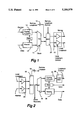
- FIG. 1 is a schematic diagram of the transmitter, according to one embodiment of the invention.
- FIG. 2 is a schematic diagram of the receiver, according to one embodiment of the invention.
- FIGS. 3 and 4 are a flow chart and a block diagram respectively of the encoder, according to one embodiment of the invention.
- FIGS. 5 and 6 are a flow chart and a block diagram respectively of the decoder, according to one embodiment of the invention.
- FIG. 7 is a schematic diagram of a framing and control circuit of the invention.
- FIG. 8 is a table showing one example of a pseudo-random pattern of the frame bits
- FIG. 9 illustrates a bi-directional link using pairs of transmitters and receivers
- FIG. 10 illustrates a bi-directional link using transmitters, receivers and repeaters.
- FIG. 11 is a schematic diagram of the transmitter including a serial encoder according to another embodiment of the invention.
- FIGS. 1 and 2 are brief functional block diagrams of a transmitter and a receiver, respectively, which form a high speed data telecommunication system.
- the figures show only parts concerning encoding/decoding multiplex/demultiplexing and framing control etc., and are only small portions of functions which are carried out in a respective semiconductor chip. Therefore in FIG. 1, there are illustrated an encoder 10 and a framing and control circuit 12, both of which are connected to a serializer 14.
- the encoder 10 receives a parallel data signal and sends an encoded data signal to the seralizer 14. At the same time, a parity check signal is sent to the framing and control circuit 12.
- the framing and control circuit 12 includes a frame pattern generator which generates frame bits in a distinct frame pattern.
- the circuit obtains control signals and mixes them with the generated frame bits.
- the mixed frame bits and control signals are sent to the serializer 14 which converts to a serial bit stream.
- a multiplexer 20 multiplexes various serial bit streams and a driver circuit 22 transmits multiplexed serial bit streams to a receiver.
- the driver circuit 22 includes amplifiers for a normal output and loopback output, the latter of which is used for system testing of the communication paths.
- the transmitter also includes a remote loopback circuit 16 to handle a remote loopback input for testing.
- FIG. 2 shows a receiver in brief diagrams.
- the serial bit streams, normal input and loopback input, from the transmitter are received and processed at a line driver 24.
- a bit stream is converted to a parallel signal at a deserializer 30.
- the deserializer 30 separates frame and control bits and data bits, both of which are respectively sent to a framing and control circuit 34 and a decoder 36.
- a loopback means 38 produces loopback control signals.
- An error signal is produced at a parity check circuit which compares signals from the framing and control circuit and the decoder.
- a remote loopback circuit 32 handles a remote loopback output for testing.
- FIGS. 3 and 4 show a flow chart and a circuit diagram, respectively, of the encoder illustrated in FIG. 1. It should be noted that the following description deals mainly with a specific embodiment of a line coding scheme of the present invention. The embodiment finds its applications chiefly in high speed telecommunication. However, similar or same line coding schemes can be used in various areas of data communications.
- the code is based on 20 bit long blocks.
- the coding does not carry across block boundaries (except to maintain dc balance).
- the 20 bits are assigned in the following manner:
- Step 1 (at box 40): Apply inversion to bits B3, B6, B7, B9, B11, B12, B13, B14, B16.
- This step is included to distribute the energy in the data spectrum for a static pattern of all zero data or all ones data, and thus to reduce EMI (Electro-Magnetic Interference).
- EMI Electro-Magnetic Interference
- Step 5 (at box 48): The dc block balance is compared to the accumulated system balance.
- the bits are inverted if the signs are the same.
- the purpose of this operation is to reduce the absolute value of the accumulated balance. It should be noted that the balance of the block can never be zero, but the system balance can. When this is the case, blocks with a positive balance are inverted at box 50, and those with a negative balance are not.
- the D bit is set if an inversion occurred, and is zero otherwise.
- Step 6 (at boxes 52): The calculated dc balance is added to the accumulated system balance if no inversion occurred and subtracted if it did (algebraic summation). (The system balance is set to zero on power up or reset.)
- Step 7 (at box 54): The frame bit is added to the D bit side of the block.
- the framing sequence is produced by a recursive 4 bit shift register, which will be shown below. This produces a sequence which is 15 bits long. Three of these 15 bits are reserved to carry control information. These three bits are identified by decoding 3 unique states of the shift register. Output [B0*, B1*, . . . , B16*, T*, D, F]
- Step 8 The block is transmitted serially.
- the F bit is transmitted first and B0 last. It should be noted that the effect of the F bit on the dc balance is ignored.
- FIG. 4 is a block diagram of the encoder, and further includes the complexity which indicates the amount of hardware which may be required to accomplish these functions.
- the complexity shown is a set of estimated values and the actual figures may vary not only in numbers but breakdowns of stages.
- FIGS. 5 and 6 the decoder functions are illustrated in FIGS. 5 and 6 as a flow chart and a circuit diagram respectively.
- the incoming serial stream is [B0*, B1*, . . . , B16*, T*, D, F].
- Step 1 Align to frame and remove frame bit.
- Output [B0*, B1*, . . . , B16*, T*, D]
- Step 3 (at box 64): Reverse the NRZI. Output: [B0', B1', . . . , B16', T']
- Output [B0, B1, . . . , B16] (16 data bits and 1 cell frame pulse bit)
- Step 5 (at box 68): Apply selective inversion to bits (B3, B6, B7, B9, B11, B12, B13, B14, B16)
- Step 6 Output parallel data.
- FIG. 6 includes a block diagram of the decoder and the complexity.
- the frame pattern is a self synchronizing pseudo-random pattern of length 15. Three of the bits will be overwritten to carry control codes.
- the frame pattern creation circuit is shown in FIG. 7.
- a set of four shift registers E0, E1, E2 and E3 are used to generate the pseudo-random bit pattern for framing.
- a control bit insertion circuit 72 which receives three control logic bits C1, C2, C3 for modifying bits in predetermined positions within the framing pattern.
- the control logic bits are used for the control of certain control functions in the data communication, such as equipment testings (loopback testings) in addition to the normal mission.
- the pseudo-random pattern of 15 bits long generated by four shift registers is shown in FIG. 8.
- a control logic bit is asserted by inverting the frame bit that would normally occur in that position. Control logic bits are not acted upon until framing is established. A strobe signal will be provided to indicate when the externally accessed control logic bits may be changed. It will occur when 1111 is held in the shift register.
- combinations of C1 and C2 are used for mission for transmitting data, and for testing the system by looping back test data through the transmitter or receiver.
- C3 is dedicated to link error monitoring.
- the parallel data is encoded, the frame and control logic bits are added, and then converted to serial format using an internally generated clock.
- the loopback modes are used for system testing of the communication paths.
- the serial data is sent through the local mate receiver to test its functionality.
- the remote loopback mode tests the serial transmission medium used in a bidirectional link.
- FIG. 9 depicts a configuration of a bi-directional link using pairs of transmitters and receivers.
- a transmitter Tx1 and receiver Rx2 are a local set located at one location, and a transmitter Tx2 and receiver Rx1 are a remote set located at another location.
- Serial data bits and other control or frame bits are sent in directions shown therein.
- a selection of control signals determines the mode of operations and selects the proper paths for such operations.
- FIG. 10 illustrates a configuration of a bi-directional link using pairs of transmitters and receivers in addition to repeaters.
- control logic bit C3 in the framing sequence carries a parity bit that covers the data after encoding (before decoding). It does not cover the frame bit. As the parity is inserted only once in a frame it covers 19*15 bits.
- the control logic bit strobe signal is used to update the parity value.
- the frame bit in the code according to the present invention does not interact with the rest of the block. This allows greater freedom in choosing the frame pattern and also the line interface part of the system design remains completely independent of data structure. Any frame length or pattern can be chosen to fit the needs of the communication system. Also, in the case where the data has been previously encoded with framing, by choosing a frame length that is not a fraction of the previous frames, the possibility of mimicking the frame pattern by static data is virtually eliminated. This method has allowed the use of a circuit which generates efficient pseudo-random codes for framing patterns.
- the length of the frame pattern and the framing state machine combine to define the average reframe and false frame times and the probability of static data imitating the frame pattern.
- the reframe time (based on average maintenance time for false frame) is less than 1 ⁇ second for frame pattern length from 4 to 32 bits.
- the time is dominated by false framing, at the longest by the time taken to load the pattern.
- the maintenance time assuming a bit error rate of 10 -14 is essentially forever.
- the frame length is not critical.
- FIGS. 1 and 2 show encoding and decoding operations on parallel data streams at the block rate, it is of course possible to perform such operations on serial data streams at the transmission rate. Therefore as shown in FIG. 11, a transmitter includes a parallel-to-serial converter which is located ahead of an encoder for the serial operations. A combiner combines the frame and encoded serial bits. A receiver can be arranged in a similar fashion for reverse operations.
- the properties of the coding scheme according to the present invention have been analyzed by a combination of analytical methods, exhaustive code combinations, and random data simulations.
- the last two methods involved computer analysis due to the number of possible data combinations in 17 bits of data (131 ⁇ 10 3 ).
- the resulting statistics on the run bound and the dc balance appear below.
- HP Hewlet-PackardTM
- FDDI 4B5B code FDDI 4B5B code. These codes are the most similar to the code according to the present invention.
- the HP code is made up of four blocks of 4B5B and can be considered as 16B20B or modified 4B5B.
- the HP code is described in detail in the Proceedings of the 1989 Bipolar Circuits and Technology Meeting on Sep. 18-19, 1989, in an article entitled "A Chipset for Gigabit Rate Data Communication" by Walker et al, pp. 288-290.
- the HP code uses 4 bits out of a 20 bit block to provide these features (20% overhead).
- the 4B5B encoding uses 20% overhead to provide the data transmission characteristics. Additional bandwidth would be needed to provide framing and control codes.
- the code according to the present invention has a minimum of 9 transitions in each 20 bit block. This gives a minimum transition density of 44% and a maximum run bound of 19. This run bound can only occur across block boundaries. It occurs very infrequently and is separated by at least 18 transitions.
- the HP code has a minimum transition density of 5% , as only one transition is guaranteed in the 20 bit block.
- the run is 20 bits. This occurs only within a block, but can occur in adjacent blocks as many times as the data remains unchanged.
- the 4B5B has a minimum transition density of 40% and a run bound of 3 bits.
- the accumulated dc imbalance cannot exceed +8, -9 bits using the code of the present invention (measured at block boundaries and not including the frame bit). Withing blocks the imbalance can reach +13 or -14 bits.
- the HP code bounds the dc imbalance to ⁇ 19 bits at block boundaries, and ⁇ 28 within block. In 4B5B code, each code has a balance of ⁇ 10%. Therefore, the code can have a dc drift of up to ⁇ 10% at all frequencies.
- dc imbalance in the transmitted signal causes the mid height of the received pulses to be shifted from set sampling point. This causes eye closure.
- ⁇ time constant of ac coupling filter (RC)
- the HP code can be reasonably estimated as requiring 2/3 the circuitry as the code of the present invention as the HP code only performs 2/3 the operations on the data.
- a rough estimate in terms of equivalent 2 input gates is 1.6k gates for the encoder, and 1k gates for the decoder. These estimates include the framing circuitry, control circuitry and retiming flip-flops.
- the alignment buffer in the receiver is estimated at 2k gates.
Abstract
Description
______________________________________ System dc Balance = 6 Next frame bit = 1 ______________________________________Input 17 Data bits 00110000011111010Step 1 00100011001000111 Selective inversion Step 2 110111001101110001 Inversion Step 3 101101000100101111 Step 4 1011010001001011110 Add D = 0 (Block Balance = 1)Step 5 0100101110110100001Inversion Step 6 System Balance = 5 Step 7 01001011101101000011 Add F = 1 or 0 ______________________________________
______________________________________
System dc Balance = 6
______________________________________
Incoming serial bits
                   01001011101101000011
Step 1             0100101110110100001
Step 2             101101000100101111
Step 3             110111001101110001
Step 4             00100011001000111
Step 5             00110000011111010
______________________________________
______________________________________ State E3 E2 E1 E0 ______________________________________C1 0 0 1 0 ControlLogic Bit C2 1 0 0 0 ControlLogic Bit C3 1 0 1 0 Control LogicBit Kick Start 0 0 0 0 Disallowed State ______________________________________
______________________________________ C2 C1 Control Code ______________________________________ 0 0 Mission (Normal Mode) 0 1 Mission (Normal Mode) 1 0 RepeaterLoopback Control Code 1 1 Remote Loopback Control Code ______________________________________
______________________________________
Bit in Error
            Result
______________________________________
F           No errors in output data, will cause
            change in Frame or Control Code state
            machine
B           Flips all bits except B16
B1-B16      Errors in bits Bn and Bn-1
B0          Errors in bit B0
______________________________________
Claims (18)
Priority Applications (6)
| Application Number | Priority Date | Filing Date | Title |
|---|---|---|---|
| US07/710,995 US5200979A (en) | 1991-06-06 | 1991-06-06 | High speed telecommunication system using a novel line code |
| PCT/CA1992/000220 WO1992022160A1 (en) | 1991-06-06 | 1992-05-27 | Line code using block inversion for high speed links |
| DE69216111T DE69216111T2 (en) | 1991-06-06 | 1992-05-27 | LINE CODE, WITH BLOCK INVERSION, FOR FAST CONNECTIONS |
| CA002109428A CA2109428C (en) | 1991-06-06 | 1992-05-27 | Line code using block inversion for high speed links |
| EP92910807A EP0610204B1 (en) | 1991-06-06 | 1992-05-27 | Line code using block inversion for high speed links |
| JP4509738A JPH06503217A (en) | 1991-06-06 | 1992-05-27 | Line code using block inversion for high speed links |
Applications Claiming Priority (1)
| Application Number | Priority Date | Filing Date | Title |
|---|---|---|---|
| US07/710,995 US5200979A (en) | 1991-06-06 | 1991-06-06 | High speed telecommunication system using a novel line code |
Publications (1)
| Publication Number | Publication Date |
|---|---|
| US5200979A true US5200979A (en) | 1993-04-06 |
Family
ID=24856361
Family Applications (1)
| Application Number | Title | Priority Date | Filing Date |
|---|---|---|---|
| US07/710,995 Expired - Lifetime US5200979A (en) | 1991-06-06 | 1991-06-06 | High speed telecommunication system using a novel line code |
Country Status (6)
| Country | Link |
|---|---|
| US (1) | US5200979A (en) |
| EP (1) | EP0610204B1 (en) |
| JP (1) | JPH06503217A (en) |
| CA (1) | CA2109428C (en) |
| DE (1) | DE69216111T2 (en) |
| WO (1) | WO1992022160A1 (en) |
Cited By (29)
| Publication number | Priority date | Publication date | Assignee | Title |
|---|---|---|---|---|
| US5327124A (en) * | 1992-05-21 | 1994-07-05 | Pioneer Electronic Corporation | Method of secondary modulation of a train of recorded data |
| US5408473A (en) * | 1992-03-03 | 1995-04-18 | Digital Equipment Corporation | Method and apparatus for transmission of communication signals over two parallel channels |
| US5412691A (en) * | 1991-06-28 | 1995-05-02 | Digital Equipment Corporation | Method and apparatus for equalization for transmission over a band-limited channel |
| US5655078A (en) * | 1994-09-30 | 1997-08-05 | Motorola Inc. | Apparatus and method for encoding data in a fiber data distributed interface (FDDI) |
| US5687356A (en) * | 1992-06-22 | 1997-11-11 | International Business Machines Corporation | Hub and interface for isochronous token ring |
| US5726993A (en) * | 1995-10-25 | 1998-03-10 | Siemens Telecom Networks | Signal detector for telephone line repeator remote loopback system |
| US5787114A (en) * | 1996-01-17 | 1998-07-28 | Lsi Logic Corporation | Loop-back test system and method |
| US5825824A (en) * | 1995-10-05 | 1998-10-20 | Silicon Image, Inc. | DC-balanced and transition-controlled encoding method and apparatus |
| US5931927A (en) * | 1996-01-08 | 1999-08-03 | Kabushiki Kaisha Toshiba | Device for reducing the fluctuation of power supply voltage due to inductance by inverting bits in groups of data lines |
| US5956370A (en) * | 1996-01-17 | 1999-09-21 | Lsi Logic Corporation | Wrap-back test system and method |
| US5974464A (en) * | 1995-10-06 | 1999-10-26 | Silicon Image, Inc. | System for high speed serial video signal transmission using DC-balanced coding |
| US5999571A (en) * | 1995-10-05 | 1999-12-07 | Silicon Image, Inc. | Transition-controlled digital encoding and signal transmission system |
| US6195764B1 (en) | 1997-01-30 | 2001-02-27 | Fujitsu Network Communications, Inc. | Data encoder/decoder for a high speed serial link |
| US6208621B1 (en) | 1997-12-16 | 2001-03-27 | Lsi Logic Corporation | Apparatus and method for testing the ability of a pair of serial data transceivers to transmit serial data at one frequency and to receive serial data at another frequency |
| US6282690B1 (en) * | 1999-01-14 | 2001-08-28 | Texas Instruments Incorporated | Parity insertion with precoder feedback in a read channel |
| US6331999B1 (en) | 1998-01-15 | 2001-12-18 | Lsi Logic Corporation | Serial data transceiver architecture and test method for measuring the amount of jitter within a serial data stream |
| US6333704B1 (en) | 1998-11-11 | 2001-12-25 | Electronics And Telecommunications Research Institute | Coding/decoding system of bit insertion/manipulation line code for high-speed optical transmission system |
| US6341142B2 (en) | 1997-12-16 | 2002-01-22 | Lsi Logic Corporation | Serial data transceiver including elements which facilitate functional testing requiring access to only the serial data ports, and an associated test method |
| KR100322474B1 (en) * | 1999-11-29 | 2002-02-07 | 오길록 | A Line Coder Circuit Using Inter-leaver Multiplexing for High Speed Data |
| US6346895B1 (en) * | 2000-10-10 | 2002-02-12 | Electronics And Telecommunications Research Institute | Apparatus and method for using nibble inversion code |
| US20030128719A1 (en) * | 2001-09-27 | 2003-07-10 | Chris Doyle | Method and apparatus for synchronous communication of frames of digital information |
| KR100425986B1 (en) * | 2001-12-24 | 2004-04-06 | 엘지전자 주식회사 | Method for Loop-Back Cut-over of AMI-coded Link in Communication System |
| US6876630B1 (en) * | 1998-12-31 | 2005-04-05 | Lg Information & Communications, Ltd. | Reframer and loss of frame (LOF) check apparatus for digital hierarchy signal |
| US6970500B1 (en) * | 2001-07-31 | 2005-11-29 | Trimble Navigation Limited | Method for determining data bit transitions for a low level spread spectrum signal |
| US7043160B1 (en) * | 2000-08-28 | 2006-05-09 | Nortel Networks Limited | Method, system and signal for carrying overhead information in a transport network employing photonic switching nodes |
| US7676725B1 (en) | 2006-02-27 | 2010-03-09 | The United States Of America As Represented By The Director, National Security Agency | Method of code generation that minimizes error propagation |
| CN1642154B (en) * | 2004-01-12 | 2010-05-12 | 联发科技股份有限公司 | Data converting device and method for converting data zone block |
| US7783937B1 (en) * | 2001-03-07 | 2010-08-24 | Marvell International Ltd. | Encoding and decoding apparatus and method with hamming weight enhancement |
| US20140077976A1 (en) * | 2012-09-18 | 2014-03-20 | Samsung Electronics Co., Ltd. | Minimum energy coding method and apparatus for performing direct current (dc) balancing in body area network or low power network |
Families Citing this family (9)
| Publication number | Priority date | Publication date | Assignee | Title |
|---|---|---|---|---|
| JP3722840B2 (en) * | 1996-03-11 | 2005-11-30 | ヒューレット・パッカード・カンパニー | Data communication apparatus and method |
| GB2357408B (en) * | 1996-07-11 | 2001-08-08 | 4Links Ltd | Communications system |
| EP0977411B1 (en) * | 1998-07-07 | 2005-04-27 | Agilent Technologies, Inc. (a Delaware corporation) | Block code with limited disparity |
| US6574731B1 (en) | 1999-03-05 | 2003-06-03 | Hewlett-Packard Company | Transmitting data words |
| US6188337B1 (en) * | 1999-06-01 | 2001-02-13 | Lucent Technologies Inc. | Low disparity coding method for digital data |
| JP4034172B2 (en) | 2002-11-20 | 2008-01-16 | Necエレクトロニクス株式会社 | Encoder, decoder and data transfer device |
| WO2005016875A2 (en) | 2003-08-06 | 2005-02-24 | Sugen, Inc. | Geometrically restricted 3-cyclopentylidene-1,3-dihydroindol-2-ones as potent protein kinase inhibitors |
| DE102006015981B4 (en) | 2005-08-19 | 2014-02-13 | Siemens Aktiengesellschaft | A method of determining the behavior of machine axes of a multi-axis machine that are moveable for movement of a tool or a tool holder |
| CA2719265A1 (en) | 2008-03-26 | 2009-10-01 | Enphase Energy, Inc. | Method and apparatus for measuring ac voltages |
Citations (6)
| Publication number | Priority date | Publication date | Assignee | Title |
|---|---|---|---|---|
| US4408189A (en) * | 1981-05-18 | 1983-10-04 | Northern Telecom Limited | Method and apparatus for code conversion of binary to multilevel signals |
| US4528550A (en) * | 1983-10-31 | 1985-07-09 | Northern Telecom Limited | Method and apparatus for code conversion of binary of multilevel signals |
| US4626826A (en) * | 1983-10-27 | 1986-12-02 | Sony Corporation | Method and apparatus for encoding and decoding an NRZI digital signal with low DC component and minimum low frequency components |
| US4682334A (en) * | 1984-05-23 | 1987-07-21 | Compagnie Industrielle Des Telecommunications Cit-Alcatel | Synchronous data transmission method and device implementing same |
| GB2232858A (en) * | 1989-05-31 | 1990-12-19 | Int Computers Ltd | Data transmission code |
| US5022051A (en) * | 1988-11-02 | 1991-06-04 | Hewlett-Packard Company | DC-free line code for arbitrary data transmission |
Family Cites Families (2)
| Publication number | Priority date | Publication date | Assignee | Title |
|---|---|---|---|---|
| US4309694A (en) * | 1980-03-27 | 1982-01-05 | Bell Telephone Laboratories, Incorporated | Zero disparity coding system |
| FR2536609A1 (en) * | 1982-11-18 | 1984-05-25 | Connan Jean Louis | Infrared digital transmission system. |
-
1991
- 1991-06-06 US US07/710,995 patent/US5200979A/en not_active Expired - Lifetime
-
1992
- 1992-05-27 DE DE69216111T patent/DE69216111T2/en not_active Expired - Fee Related
- 1992-05-27 WO PCT/CA1992/000220 patent/WO1992022160A1/en active IP Right Grant
- 1992-05-27 JP JP4509738A patent/JPH06503217A/en active Pending
- 1992-05-27 CA CA002109428A patent/CA2109428C/en not_active Expired - Fee Related
- 1992-05-27 EP EP92910807A patent/EP0610204B1/en not_active Expired - Lifetime
Patent Citations (6)
| Publication number | Priority date | Publication date | Assignee | Title |
|---|---|---|---|---|
| US4408189A (en) * | 1981-05-18 | 1983-10-04 | Northern Telecom Limited | Method and apparatus for code conversion of binary to multilevel signals |
| US4626826A (en) * | 1983-10-27 | 1986-12-02 | Sony Corporation | Method and apparatus for encoding and decoding an NRZI digital signal with low DC component and minimum low frequency components |
| US4528550A (en) * | 1983-10-31 | 1985-07-09 | Northern Telecom Limited | Method and apparatus for code conversion of binary of multilevel signals |
| US4682334A (en) * | 1984-05-23 | 1987-07-21 | Compagnie Industrielle Des Telecommunications Cit-Alcatel | Synchronous data transmission method and device implementing same |
| US5022051A (en) * | 1988-11-02 | 1991-06-04 | Hewlett-Packard Company | DC-free line code for arbitrary data transmission |
| GB2232858A (en) * | 1989-05-31 | 1990-12-19 | Int Computers Ltd | Data transmission code |
Non-Patent Citations (2)
| Title |
|---|
| Publication: "A Chipset for Gigabit Rate Data Communication" by R. C. Walker et al., Proceedings of the 1989 Bipolar Circuits & Technology Meeting, IEEE, Sep. 18-19, 1989, pp. 288-290. |
| Publication: A Chipset for Gigabit Rate Data Communication by R. C. Walker et al., Proceedings of the 1989 Bipolar Circuits & Technology Meeting, IEEE, Sep. 18 19, 1989, pp. 288 290. * |
Cited By (36)
| Publication number | Priority date | Publication date | Assignee | Title |
|---|---|---|---|---|
| US5412691A (en) * | 1991-06-28 | 1995-05-02 | Digital Equipment Corporation | Method and apparatus for equalization for transmission over a band-limited channel |
| US5408473A (en) * | 1992-03-03 | 1995-04-18 | Digital Equipment Corporation | Method and apparatus for transmission of communication signals over two parallel channels |
| US5327124A (en) * | 1992-05-21 | 1994-07-05 | Pioneer Electronic Corporation | Method of secondary modulation of a train of recorded data |
| US5687356A (en) * | 1992-06-22 | 1997-11-11 | International Business Machines Corporation | Hub and interface for isochronous token ring |
| US5655078A (en) * | 1994-09-30 | 1997-08-05 | Motorola Inc. | Apparatus and method for encoding data in a fiber data distributed interface (FDDI) |
| US5999571A (en) * | 1995-10-05 | 1999-12-07 | Silicon Image, Inc. | Transition-controlled digital encoding and signal transmission system |
| US5825824A (en) * | 1995-10-05 | 1998-10-20 | Silicon Image, Inc. | DC-balanced and transition-controlled encoding method and apparatus |
| US6026124A (en) * | 1995-10-05 | 2000-02-15 | Silicon Image, Inc. | Transition-controlled digital encoding and signal transmission system |
| US5974464A (en) * | 1995-10-06 | 1999-10-26 | Silicon Image, Inc. | System for high speed serial video signal transmission using DC-balanced coding |
| US5726993A (en) * | 1995-10-25 | 1998-03-10 | Siemens Telecom Networks | Signal detector for telephone line repeator remote loopback system |
| US5931927A (en) * | 1996-01-08 | 1999-08-03 | Kabushiki Kaisha Toshiba | Device for reducing the fluctuation of power supply voltage due to inductance by inverting bits in groups of data lines |
| US5787114A (en) * | 1996-01-17 | 1998-07-28 | Lsi Logic Corporation | Loop-back test system and method |
| US5956370A (en) * | 1996-01-17 | 1999-09-21 | Lsi Logic Corporation | Wrap-back test system and method |
| US6195764B1 (en) | 1997-01-30 | 2001-02-27 | Fujitsu Network Communications, Inc. | Data encoder/decoder for a high speed serial link |
| US6425107B1 (en) | 1997-01-30 | 2002-07-23 | Fujitsu Network Communications, Inc. | Data encoder/decoder for a high speed serial link |
| US6341142B2 (en) | 1997-12-16 | 2002-01-22 | Lsi Logic Corporation | Serial data transceiver including elements which facilitate functional testing requiring access to only the serial data ports, and an associated test method |
| US6208621B1 (en) | 1997-12-16 | 2001-03-27 | Lsi Logic Corporation | Apparatus and method for testing the ability of a pair of serial data transceivers to transmit serial data at one frequency and to receive serial data at another frequency |
| US6331999B1 (en) | 1998-01-15 | 2001-12-18 | Lsi Logic Corporation | Serial data transceiver architecture and test method for measuring the amount of jitter within a serial data stream |
| US6333704B1 (en) | 1998-11-11 | 2001-12-25 | Electronics And Telecommunications Research Institute | Coding/decoding system of bit insertion/manipulation line code for high-speed optical transmission system |
| US6876630B1 (en) * | 1998-12-31 | 2005-04-05 | Lg Information & Communications, Ltd. | Reframer and loss of frame (LOF) check apparatus for digital hierarchy signal |
| US6282690B1 (en) * | 1999-01-14 | 2001-08-28 | Texas Instruments Incorporated | Parity insertion with precoder feedback in a read channel |
| KR100322474B1 (en) * | 1999-11-29 | 2002-02-07 | 오길록 | A Line Coder Circuit Using Inter-leaver Multiplexing for High Speed Data |
| US7043160B1 (en) * | 2000-08-28 | 2006-05-09 | Nortel Networks Limited | Method, system and signal for carrying overhead information in a transport network employing photonic switching nodes |
| US6346895B1 (en) * | 2000-10-10 | 2002-02-12 | Electronics And Telecommunications Research Institute | Apparatus and method for using nibble inversion code |
| US8359498B1 (en) * | 2001-03-07 | 2013-01-22 | Marvell International Ltd. | Encoding and decoding apparatus and method with hamming weight enhancement |
| US7783937B1 (en) * | 2001-03-07 | 2010-08-24 | Marvell International Ltd. | Encoding and decoding apparatus and method with hamming weight enhancement |
| US7802151B1 (en) * | 2001-03-07 | 2010-09-21 | Marvell International Ltd. | Encoding and decoding apparatus and method with hamming weight enhancement |
| US6970500B1 (en) * | 2001-07-31 | 2005-11-29 | Trimble Navigation Limited | Method for determining data bit transitions for a low level spread spectrum signal |
| US7266144B1 (en) | 2001-07-31 | 2007-09-04 | Sanders Jeffrey D | Data bit transition determination method and apparatus for spread spectrum signals |
| US20030128719A1 (en) * | 2001-09-27 | 2003-07-10 | Chris Doyle | Method and apparatus for synchronous communication of frames of digital information |
| US9019899B2 (en) * | 2001-09-27 | 2015-04-28 | Alcatel Lucent | Method and apparatus for synchronous communication of frames of digital information |
| KR100425986B1 (en) * | 2001-12-24 | 2004-04-06 | 엘지전자 주식회사 | Method for Loop-Back Cut-over of AMI-coded Link in Communication System |
| CN1642154B (en) * | 2004-01-12 | 2010-05-12 | 联发科技股份有限公司 | Data converting device and method for converting data zone block |
| US7676725B1 (en) | 2006-02-27 | 2010-03-09 | The United States Of America As Represented By The Director, National Security Agency | Method of code generation that minimizes error propagation |
| US20140077976A1 (en) * | 2012-09-18 | 2014-03-20 | Samsung Electronics Co., Ltd. | Minimum energy coding method and apparatus for performing direct current (dc) balancing in body area network or low power network |
| US8902088B2 (en) * | 2012-09-18 | 2014-12-02 | Samsung Electronics Co., Ltd. | Minimum energy coding method and apparatus for performing direct current (DC) balancing in body area network or low power network |
Also Published As
| Publication number | Publication date |
|---|---|
| WO1992022160A1 (en) | 1992-12-10 |
| DE69216111D1 (en) | 1997-01-30 |
| CA2109428A1 (en) | 1992-12-07 |
| CA2109428C (en) | 1998-09-15 |
| EP0610204A1 (en) | 1994-08-17 |
| EP0610204B1 (en) | 1996-12-18 |
| DE69216111T2 (en) | 1997-04-17 |
| JPH06503217A (en) | 1994-04-07 |
Similar Documents
| Publication | Publication Date | Title |
|---|---|---|
| US5200979A (en) | High speed telecommunication system using a novel line code | |
| US6496540B1 (en) | Transformation of parallel interface into coded format with preservation of baud-rate | |
| CA1289249C (en) | Parallel transmission system | |
| Widmer et al. | A DC-balanced, partitioned-block, 8B/10B transmission code | |
| US4486739A (en) | Byte oriented DC balanced (0,4) 8B/10B partitioned block transmission code | |
| US4979185A (en) | High speed serial data link | |
| EP1830531B1 (en) | Precoding circuit and precoding-multiplexing circuit for realizing very high transmission rate in optical fiber communication | |
| EP0977411B1 (en) | Block code with limited disparity | |
| KR100279752B1 (en) | Encoding / Decoding Device of Bit Insertion / Operation Line Code for High Speed Optical Transmission System | |
| JP2538524B2 (en) | Signal decoding method and apparatus | |
| US4524462A (en) | System for jointly transmitting high-frequency and low-frequency digital signals over a fiber-optical carrier | |
| US4791407A (en) | Alternate mark/space inversion line code | |
| CA1269733A (en) | Digital signal transmission system having frame synchronization operation | |
| US5629983A (en) | Parallel transmission through plurality of optical fibers | |
| CA2031494C (en) | Correlation code transmission system | |
| JPS59183559A (en) | Digital transmitter | |
| US5742135A (en) | System for maintaining polarity synchronization during AMI data transfer | |
| GB2174577A (en) | Digital communication system | |
| US20020186322A1 (en) | Method of adding data to a data communication link while retaining backward compatibility | |
| CN111800637A (en) | System and method for realizing HDB3 encoding and decoding by using FPGA | |
| US5309475A (en) | Data interchange network | |
| US6049571A (en) | Encoding circuit with a function of zero continuous-suppression in a data transmission system | |
| Waters | Invited paper Line codes for metallic cable systems | |
| KR0141918B1 (en) | High speed serial data link | |
| JP2834246B2 (en) | Correlation code transmission system |
Legal Events
| Date | Code | Title | Description |
|---|---|---|---|
| AS | Assignment |
Owner name: NORTHERN TELECOM LIMITED Free format text: ASSIGNMENT OF ASSIGNORS INTEREST.;ASSIGNOR:BELL-NORTHERN RESEARCH LTD.;REEL/FRAME:005945/0213 Effective date: 19911125 Owner name: BELL-NORTHERN RESEARCH LTD. Free format text: ASSIGNMENT OF ASSIGNORS INTEREST.;ASSIGNOR:HARRIS, GWENDOLYN K.;REEL/FRAME:005945/0211 Effective date: 19911118 |
|
| STCF | Information on status: patent grant |
Free format text: PATENTED CASE |
|
| FEPP | Fee payment procedure |
Free format text: PAYOR NUMBER ASSIGNED (ORIGINAL EVENT CODE: ASPN); ENTITY STATUS OF PATENT OWNER: LARGE ENTITY |
|
| FPAY | Fee payment |
Year of fee payment: 4 |
|
| AS | Assignment |
Owner name: NORTEL NETWORKS CORPORATION, CANADA Free format text: CHANGE OF NAME;ASSIGNOR:NORTHERN TELECOM LIMITED;REEL/FRAME:010567/0001 Effective date: 19990429 |
|
| AS | Assignment |
Owner name: NORTEL NETWORKS LIMITED, CANADA Free format text: CHANGE OF NAME;ASSIGNOR:NORTEL NETWORKS CORPORATION;REEL/FRAME:011195/0706 Effective date: 20000830 Owner name: NORTEL NETWORKS LIMITED,CANADA Free format text: CHANGE OF NAME;ASSIGNOR:NORTEL NETWORKS CORPORATION;REEL/FRAME:011195/0706 Effective date: 20000830 |
|
| FPAY | Fee payment |
Year of fee payment: 8 |
|
| FPAY | Fee payment |
Year of fee payment: 12 |