US5205032A - Electronic parts mounting apparatus - Google Patents
Electronic parts mounting apparatus Download PDFInfo
- Publication number
- US5205032A US5205032A US07/766,204 US76620491A US5205032A US 5205032 A US5205032 A US 5205032A US 76620491 A US76620491 A US 76620491A US 5205032 A US5205032 A US 5205032A
- Authority
- US
- United States
- Prior art keywords
- recessed portion
- substrate
- bonding
- mount body
- electronic part
- Prior art date
- Legal status (The legal status is an assumption and is not a legal conclusion. Google has not performed a legal analysis and makes no representation as to the accuracy of the status listed.)
- Expired - Lifetime
Links
Images


Classifications
-
- H—ELECTRICITY
- H01—ELECTRIC ELEMENTS
- H01L—SEMICONDUCTOR DEVICES NOT COVERED BY CLASS H10
- H01L24/00—Arrangements for connecting or disconnecting semiconductor or solid-state bodies; Methods or apparatus related thereto
- H01L24/80—Methods for connecting semiconductor or other solid state bodies using means for bonding being attached to, or being formed on, the surface to be connected
- H01L24/81—Methods for connecting semiconductor or other solid state bodies using means for bonding being attached to, or being formed on, the surface to be connected using a bump connector
-
- H—ELECTRICITY
- H01—ELECTRIC ELEMENTS
- H01L—SEMICONDUCTOR DEVICES NOT COVERED BY CLASS H10
- H01L23/00—Details of semiconductor or other solid state devices
- H01L23/12—Mountings, e.g. non-detachable insulating substrates
- H01L23/13—Mountings, e.g. non-detachable insulating substrates characterised by the shape
-
- H—ELECTRICITY
- H01—ELECTRIC ELEMENTS
- H01L—SEMICONDUCTOR DEVICES NOT COVERED BY CLASS H10
- H01L24/00—Arrangements for connecting or disconnecting semiconductor or solid-state bodies; Methods or apparatus related thereto
- H01L24/01—Means for bonding being attached to, or being formed on, the surface to be connected, e.g. chip-to-package, die-attach, "first-level" interconnects; Manufacturing methods related thereto
- H01L24/26—Layer connectors, e.g. plate connectors, solder or adhesive layers; Manufacturing methods related thereto
- H01L24/28—Structure, shape, material or disposition of the layer connectors prior to the connecting process
- H01L24/29—Structure, shape, material or disposition of the layer connectors prior to the connecting process of an individual layer connector
-
- H—ELECTRICITY
- H01—ELECTRIC ELEMENTS
- H01L—SEMICONDUCTOR DEVICES NOT COVERED BY CLASS H10
- H01L24/00—Arrangements for connecting or disconnecting semiconductor or solid-state bodies; Methods or apparatus related thereto
- H01L24/74—Apparatus for manufacturing arrangements for connecting or disconnecting semiconductor or solid-state bodies
- H01L24/75—Apparatus for connecting with bump connectors or layer connectors
-
- H—ELECTRICITY
- H01—ELECTRIC ELEMENTS
- H01L—SEMICONDUCTOR DEVICES NOT COVERED BY CLASS H10
- H01L24/00—Arrangements for connecting or disconnecting semiconductor or solid-state bodies; Methods or apparatus related thereto
- H01L24/80—Methods for connecting semiconductor or other solid state bodies using means for bonding being attached to, or being formed on, the surface to be connected
- H01L24/83—Methods for connecting semiconductor or other solid state bodies using means for bonding being attached to, or being formed on, the surface to be connected using a layer connector
-
- H—ELECTRICITY
- H01—ELECTRIC ELEMENTS
- H01L—SEMICONDUCTOR DEVICES NOT COVERED BY CLASS H10
- H01L24/00—Arrangements for connecting or disconnecting semiconductor or solid-state bodies; Methods or apparatus related thereto
- H01L24/80—Methods for connecting semiconductor or other solid state bodies using means for bonding being attached to, or being formed on, the surface to be connected
- H01L24/85—Methods for connecting semiconductor or other solid state bodies using means for bonding being attached to, or being formed on, the surface to be connected using a wire connector
-
- H—ELECTRICITY
- H01—ELECTRIC ELEMENTS
- H01L—SEMICONDUCTOR DEVICES NOT COVERED BY CLASS H10
- H01L2224/00—Indexing scheme for arrangements for connecting or disconnecting semiconductor or solid-state bodies and methods related thereto as covered by H01L24/00
- H01L2224/01—Means for bonding being attached to, or being formed on, the surface to be connected, e.g. chip-to-package, die-attach, "first-level" interconnects; Manufacturing methods related thereto
- H01L2224/10—Bump connectors; Manufacturing methods related thereto
- H01L2224/15—Structure, shape, material or disposition of the bump connectors after the connecting process
- H01L2224/16—Structure, shape, material or disposition of the bump connectors after the connecting process of an individual bump connector
- H01L2224/161—Disposition
- H01L2224/16151—Disposition the bump connector connecting between a semiconductor or solid-state body and an item not being a semiconductor or solid-state body, e.g. chip-to-substrate, chip-to-passive
- H01L2224/16221—Disposition the bump connector connecting between a semiconductor or solid-state body and an item not being a semiconductor or solid-state body, e.g. chip-to-substrate, chip-to-passive the body and the item being stacked
- H01L2224/16225—Disposition the bump connector connecting between a semiconductor or solid-state body and an item not being a semiconductor or solid-state body, e.g. chip-to-substrate, chip-to-passive the body and the item being stacked the item being non-metallic, e.g. insulating substrate with or without metallisation
-
- H—ELECTRICITY
- H01—ELECTRIC ELEMENTS
- H01L—SEMICONDUCTOR DEVICES NOT COVERED BY CLASS H10
- H01L2224/00—Indexing scheme for arrangements for connecting or disconnecting semiconductor or solid-state bodies and methods related thereto as covered by H01L24/00
- H01L2224/01—Means for bonding being attached to, or being formed on, the surface to be connected, e.g. chip-to-package, die-attach, "first-level" interconnects; Manufacturing methods related thereto
- H01L2224/26—Layer connectors, e.g. plate connectors, solder or adhesive layers; Manufacturing methods related thereto
- H01L2224/28—Structure, shape, material or disposition of the layer connectors prior to the connecting process
- H01L2224/29—Structure, shape, material or disposition of the layer connectors prior to the connecting process of an individual layer connector
- H01L2224/29001—Core members of the layer connector
- H01L2224/29099—Material
- H01L2224/291—Material with a principal constituent of the material being a metal or a metalloid, e.g. boron [B], silicon [Si], germanium [Ge], arsenic [As], antimony [Sb], tellurium [Te] and polonium [Po], and alloys thereof
- H01L2224/29101—Material with a principal constituent of the material being a metal or a metalloid, e.g. boron [B], silicon [Si], germanium [Ge], arsenic [As], antimony [Sb], tellurium [Te] and polonium [Po], and alloys thereof the principal constituent melting at a temperature of less than 400°C
- H01L2224/29111—Tin [Sn] as principal constituent
-
- H—ELECTRICITY
- H01—ELECTRIC ELEMENTS
- H01L—SEMICONDUCTOR DEVICES NOT COVERED BY CLASS H10
- H01L2224/00—Indexing scheme for arrangements for connecting or disconnecting semiconductor or solid-state bodies and methods related thereto as covered by H01L24/00
- H01L2224/01—Means for bonding being attached to, or being formed on, the surface to be connected, e.g. chip-to-package, die-attach, "first-level" interconnects; Manufacturing methods related thereto
- H01L2224/42—Wire connectors; Manufacturing methods related thereto
- H01L2224/47—Structure, shape, material or disposition of the wire connectors after the connecting process
- H01L2224/48—Structure, shape, material or disposition of the wire connectors after the connecting process of an individual wire connector
- H01L2224/4805—Shape
- H01L2224/4809—Loop shape
- H01L2224/48091—Arched
-
- H—ELECTRICITY
- H01—ELECTRIC ELEMENTS
- H01L—SEMICONDUCTOR DEVICES NOT COVERED BY CLASS H10
- H01L2224/00—Indexing scheme for arrangements for connecting or disconnecting semiconductor or solid-state bodies and methods related thereto as covered by H01L24/00
- H01L2224/01—Means for bonding being attached to, or being formed on, the surface to be connected, e.g. chip-to-package, die-attach, "first-level" interconnects; Manufacturing methods related thereto
- H01L2224/42—Wire connectors; Manufacturing methods related thereto
- H01L2224/47—Structure, shape, material or disposition of the wire connectors after the connecting process
- H01L2224/48—Structure, shape, material or disposition of the wire connectors after the connecting process of an individual wire connector
- H01L2224/481—Disposition
- H01L2224/48151—Connecting between a semiconductor or solid-state body and an item not being a semiconductor or solid-state body, e.g. chip-to-substrate, chip-to-passive
- H01L2224/48221—Connecting between a semiconductor or solid-state body and an item not being a semiconductor or solid-state body, e.g. chip-to-substrate, chip-to-passive the body and the item being stacked
- H01L2224/48225—Connecting between a semiconductor or solid-state body and an item not being a semiconductor or solid-state body, e.g. chip-to-substrate, chip-to-passive the body and the item being stacked the item being non-metallic, e.g. insulating substrate with or without metallisation
- H01L2224/48227—Connecting between a semiconductor or solid-state body and an item not being a semiconductor or solid-state body, e.g. chip-to-substrate, chip-to-passive the body and the item being stacked the item being non-metallic, e.g. insulating substrate with or without metallisation connecting the wire to a bond pad of the item
-
- H—ELECTRICITY
- H01—ELECTRIC ELEMENTS
- H01L—SEMICONDUCTOR DEVICES NOT COVERED BY CLASS H10
- H01L2224/00—Indexing scheme for arrangements for connecting or disconnecting semiconductor or solid-state bodies and methods related thereto as covered by H01L24/00
- H01L2224/01—Means for bonding being attached to, or being formed on, the surface to be connected, e.g. chip-to-package, die-attach, "first-level" interconnects; Manufacturing methods related thereto
- H01L2224/42—Wire connectors; Manufacturing methods related thereto
- H01L2224/47—Structure, shape, material or disposition of the wire connectors after the connecting process
- H01L2224/48—Structure, shape, material or disposition of the wire connectors after the connecting process of an individual wire connector
- H01L2224/481—Disposition
- H01L2224/48151—Connecting between a semiconductor or solid-state body and an item not being a semiconductor or solid-state body, e.g. chip-to-substrate, chip-to-passive
- H01L2224/48221—Connecting between a semiconductor or solid-state body and an item not being a semiconductor or solid-state body, e.g. chip-to-substrate, chip-to-passive the body and the item being stacked
- H01L2224/48225—Connecting between a semiconductor or solid-state body and an item not being a semiconductor or solid-state body, e.g. chip-to-substrate, chip-to-passive the body and the item being stacked the item being non-metallic, e.g. insulating substrate with or without metallisation
- H01L2224/4824—Connecting between the body and an opposite side of the item with respect to the body
-
- H—ELECTRICITY
- H01—ELECTRIC ELEMENTS
- H01L—SEMICONDUCTOR DEVICES NOT COVERED BY CLASS H10
- H01L2224/00—Indexing scheme for arrangements for connecting or disconnecting semiconductor or solid-state bodies and methods related thereto as covered by H01L24/00
- H01L2224/74—Apparatus for manufacturing arrangements for connecting or disconnecting semiconductor or solid-state bodies and for methods related thereto
- H01L2224/75—Apparatus for connecting with bump connectors or layer connectors
- H01L2224/7525—Means for applying energy, e.g. heating means
- H01L2224/753—Means for applying energy, e.g. heating means by means of pressure
- H01L2224/75301—Bonding head
- H01L2224/75302—Shape
- H01L2224/75303—Shape of the pressing surface
-
- H—ELECTRICITY
- H01—ELECTRIC ELEMENTS
- H01L—SEMICONDUCTOR DEVICES NOT COVERED BY CLASS H10
- H01L2224/00—Indexing scheme for arrangements for connecting or disconnecting semiconductor or solid-state bodies and methods related thereto as covered by H01L24/00
- H01L2224/80—Methods for connecting semiconductor or other solid state bodies using means for bonding being attached to, or being formed on, the surface to be connected
- H01L2224/81—Methods for connecting semiconductor or other solid state bodies using means for bonding being attached to, or being formed on, the surface to be connected using a bump connector
- H01L2224/818—Bonding techniques
- H01L2224/81801—Soldering or alloying
-
- H—ELECTRICITY
- H01—ELECTRIC ELEMENTS
- H01L—SEMICONDUCTOR DEVICES NOT COVERED BY CLASS H10
- H01L2224/00—Indexing scheme for arrangements for connecting or disconnecting semiconductor or solid-state bodies and methods related thereto as covered by H01L24/00
- H01L2224/80—Methods for connecting semiconductor or other solid state bodies using means for bonding being attached to, or being formed on, the surface to be connected
- H01L2224/83—Methods for connecting semiconductor or other solid state bodies using means for bonding being attached to, or being formed on, the surface to be connected using a layer connector
- H01L2224/8319—Arrangement of the layer connectors prior to mounting
- H01L2224/83191—Arrangement of the layer connectors prior to mounting wherein the layer connectors are disposed only on the semiconductor or solid-state body
-
- H—ELECTRICITY
- H01—ELECTRIC ELEMENTS
- H01L—SEMICONDUCTOR DEVICES NOT COVERED BY CLASS H10
- H01L2224/00—Indexing scheme for arrangements for connecting or disconnecting semiconductor or solid-state bodies and methods related thereto as covered by H01L24/00
- H01L2224/80—Methods for connecting semiconductor or other solid state bodies using means for bonding being attached to, or being formed on, the surface to be connected
- H01L2224/83—Methods for connecting semiconductor or other solid state bodies using means for bonding being attached to, or being formed on, the surface to be connected using a layer connector
- H01L2224/838—Bonding techniques
- H01L2224/8385—Bonding techniques using a polymer adhesive, e.g. an adhesive based on silicone, epoxy, polyimide, polyester
-
- H—ELECTRICITY
- H01—ELECTRIC ELEMENTS
- H01L—SEMICONDUCTOR DEVICES NOT COVERED BY CLASS H10
- H01L2224/00—Indexing scheme for arrangements for connecting or disconnecting semiconductor or solid-state bodies and methods related thereto as covered by H01L24/00
- H01L2224/80—Methods for connecting semiconductor or other solid state bodies using means for bonding being attached to, or being formed on, the surface to be connected
- H01L2224/85—Methods for connecting semiconductor or other solid state bodies using means for bonding being attached to, or being formed on, the surface to be connected using a wire connector
- H01L2224/852—Applying energy for connecting
- H01L2224/85201—Compression bonding
- H01L2224/85205—Ultrasonic bonding
-
- H—ELECTRICITY
- H01—ELECTRIC ELEMENTS
- H01L—SEMICONDUCTOR DEVICES NOT COVERED BY CLASS H10
- H01L24/00—Arrangements for connecting or disconnecting semiconductor or solid-state bodies; Methods or apparatus related thereto
- H01L24/01—Means for bonding being attached to, or being formed on, the surface to be connected, e.g. chip-to-package, die-attach, "first-level" interconnects; Manufacturing methods related thereto
- H01L24/42—Wire connectors; Manufacturing methods related thereto
- H01L24/47—Structure, shape, material or disposition of the wire connectors after the connecting process
- H01L24/48—Structure, shape, material or disposition of the wire connectors after the connecting process of an individual wire connector
-
- H—ELECTRICITY
- H01—ELECTRIC ELEMENTS
- H01L—SEMICONDUCTOR DEVICES NOT COVERED BY CLASS H10
- H01L2924/00—Indexing scheme for arrangements or methods for connecting or disconnecting semiconductor or solid-state bodies as covered by H01L24/00
- H01L2924/0001—Technical content checked by a classifier
- H01L2924/00014—Technical content checked by a classifier the subject-matter covered by the group, the symbol of which is combined with the symbol of this group, being disclosed without further technical details
-
- H—ELECTRICITY
- H01—ELECTRIC ELEMENTS
- H01L—SEMICONDUCTOR DEVICES NOT COVERED BY CLASS H10
- H01L2924/00—Indexing scheme for arrangements or methods for connecting or disconnecting semiconductor or solid-state bodies as covered by H01L24/00
- H01L2924/01—Chemical elements
- H01L2924/01005—Boron [B]
-
- H—ELECTRICITY
- H01—ELECTRIC ELEMENTS
- H01L—SEMICONDUCTOR DEVICES NOT COVERED BY CLASS H10
- H01L2924/00—Indexing scheme for arrangements or methods for connecting or disconnecting semiconductor or solid-state bodies as covered by H01L24/00
- H01L2924/01—Chemical elements
- H01L2924/01006—Carbon [C]
-
- H—ELECTRICITY
- H01—ELECTRIC ELEMENTS
- H01L—SEMICONDUCTOR DEVICES NOT COVERED BY CLASS H10
- H01L2924/00—Indexing scheme for arrangements or methods for connecting or disconnecting semiconductor or solid-state bodies as covered by H01L24/00
- H01L2924/01—Chemical elements
- H01L2924/01007—Nitrogen [N]
-
- H—ELECTRICITY
- H01—ELECTRIC ELEMENTS
- H01L—SEMICONDUCTOR DEVICES NOT COVERED BY CLASS H10
- H01L2924/00—Indexing scheme for arrangements or methods for connecting or disconnecting semiconductor or solid-state bodies as covered by H01L24/00
- H01L2924/01—Chemical elements
- H01L2924/01014—Silicon [Si]
-
- H—ELECTRICITY
- H01—ELECTRIC ELEMENTS
- H01L—SEMICONDUCTOR DEVICES NOT COVERED BY CLASS H10
- H01L2924/00—Indexing scheme for arrangements or methods for connecting or disconnecting semiconductor or solid-state bodies as covered by H01L24/00
- H01L2924/01—Chemical elements
- H01L2924/01029—Copper [Cu]
-
- H—ELECTRICITY
- H01—ELECTRIC ELEMENTS
- H01L—SEMICONDUCTOR DEVICES NOT COVERED BY CLASS H10
- H01L2924/00—Indexing scheme for arrangements or methods for connecting or disconnecting semiconductor or solid-state bodies as covered by H01L24/00
- H01L2924/01—Chemical elements
- H01L2924/01032—Germanium [Ge]
-
- H—ELECTRICITY
- H01—ELECTRIC ELEMENTS
- H01L—SEMICONDUCTOR DEVICES NOT COVERED BY CLASS H10
- H01L2924/00—Indexing scheme for arrangements or methods for connecting or disconnecting semiconductor or solid-state bodies as covered by H01L24/00
- H01L2924/01—Chemical elements
- H01L2924/01033—Arsenic [As]
-
- H—ELECTRICITY
- H01—ELECTRIC ELEMENTS
- H01L—SEMICONDUCTOR DEVICES NOT COVERED BY CLASS H10
- H01L2924/00—Indexing scheme for arrangements or methods for connecting or disconnecting semiconductor or solid-state bodies as covered by H01L24/00
- H01L2924/01—Chemical elements
- H01L2924/01039—Yttrium [Y]
-
- H—ELECTRICITY
- H01—ELECTRIC ELEMENTS
- H01L—SEMICONDUCTOR DEVICES NOT COVERED BY CLASS H10
- H01L2924/00—Indexing scheme for arrangements or methods for connecting or disconnecting semiconductor or solid-state bodies as covered by H01L24/00
- H01L2924/01—Chemical elements
- H01L2924/0105—Tin [Sn]
-
- H—ELECTRICITY
- H01—ELECTRIC ELEMENTS
- H01L—SEMICONDUCTOR DEVICES NOT COVERED BY CLASS H10
- H01L2924/00—Indexing scheme for arrangements or methods for connecting or disconnecting semiconductor or solid-state bodies as covered by H01L24/00
- H01L2924/01—Chemical elements
- H01L2924/01079—Gold [Au]
-
- H—ELECTRICITY
- H01—ELECTRIC ELEMENTS
- H01L—SEMICONDUCTOR DEVICES NOT COVERED BY CLASS H10
- H01L2924/00—Indexing scheme for arrangements or methods for connecting or disconnecting semiconductor or solid-state bodies as covered by H01L24/00
- H01L2924/013—Alloys
- H01L2924/0132—Binary Alloys
-
- H—ELECTRICITY
- H01—ELECTRIC ELEMENTS
- H01L—SEMICONDUCTOR DEVICES NOT COVERED BY CLASS H10
- H01L2924/00—Indexing scheme for arrangements or methods for connecting or disconnecting semiconductor or solid-state bodies as covered by H01L24/00
- H01L2924/013—Alloys
- H01L2924/014—Solder alloys
-
- H—ELECTRICITY
- H01—ELECTRIC ELEMENTS
- H01L—SEMICONDUCTOR DEVICES NOT COVERED BY CLASS H10
- H01L2924/00—Indexing scheme for arrangements or methods for connecting or disconnecting semiconductor or solid-state bodies as covered by H01L24/00
- H01L2924/06—Polymers
- H01L2924/078—Adhesive characteristics other than chemical
- H01L2924/07802—Adhesive characteristics other than chemical not being an ohmic electrical conductor
-
- H—ELECTRICITY
- H01—ELECTRIC ELEMENTS
- H01L—SEMICONDUCTOR DEVICES NOT COVERED BY CLASS H10
- H01L2924/00—Indexing scheme for arrangements or methods for connecting or disconnecting semiconductor or solid-state bodies as covered by H01L24/00
- H01L2924/10—Details of semiconductor or other solid state devices to be connected
- H01L2924/102—Material of the semiconductor or solid state bodies
- H01L2924/1025—Semiconducting materials
- H01L2924/1026—Compound semiconductors
- H01L2924/1032—III-V
- H01L2924/10329—Gallium arsenide [GaAs]
-
- H—ELECTRICITY
- H01—ELECTRIC ELEMENTS
- H01L—SEMICONDUCTOR DEVICES NOT COVERED BY CLASS H10
- H01L2924/00—Indexing scheme for arrangements or methods for connecting or disconnecting semiconductor or solid-state bodies as covered by H01L24/00
- H01L2924/10—Details of semiconductor or other solid state devices to be connected
- H01L2924/11—Device type
- H01L2924/12—Passive devices, e.g. 2 terminal devices
- H01L2924/1204—Optical Diode
- H01L2924/12041—LED
-
- H—ELECTRICITY
- H01—ELECTRIC ELEMENTS
- H01L—SEMICONDUCTOR DEVICES NOT COVERED BY CLASS H10
- H01L2924/00—Indexing scheme for arrangements or methods for connecting or disconnecting semiconductor or solid-state bodies as covered by H01L24/00
- H01L2924/10—Details of semiconductor or other solid state devices to be connected
- H01L2924/11—Device type
- H01L2924/12—Passive devices, e.g. 2 terminal devices
- H01L2924/1204—Optical Diode
- H01L2924/12042—LASER
-
- H—ELECTRICITY
- H01—ELECTRIC ELEMENTS
- H01L—SEMICONDUCTOR DEVICES NOT COVERED BY CLASS H10
- H01L2924/00—Indexing scheme for arrangements or methods for connecting or disconnecting semiconductor or solid-state bodies as covered by H01L24/00
- H01L2924/10—Details of semiconductor or other solid state devices to be connected
- H01L2924/11—Device type
- H01L2924/12—Passive devices, e.g. 2 terminal devices
- H01L2924/1204—Optical Diode
- H01L2924/12043—Photo diode
-
- H—ELECTRICITY
- H01—ELECTRIC ELEMENTS
- H01L—SEMICONDUCTOR DEVICES NOT COVERED BY CLASS H10
- H01L2924/00—Indexing scheme for arrangements or methods for connecting or disconnecting semiconductor or solid-state bodies as covered by H01L24/00
- H01L2924/15—Details of package parts other than the semiconductor or other solid state devices to be connected
- H01L2924/151—Die mounting substrate
- H01L2924/1515—Shape
- H01L2924/15153—Shape the die mounting substrate comprising a recess for hosting the device
- H01L2924/15155—Shape the die mounting substrate comprising a recess for hosting the device the shape of the recess being other than a cuboid
- H01L2924/15156—Side view
-
- H—ELECTRICITY
- H01—ELECTRIC ELEMENTS
- H01L—SEMICONDUCTOR DEVICES NOT COVERED BY CLASS H10
- H01L2924/00—Indexing scheme for arrangements or methods for connecting or disconnecting semiconductor or solid-state bodies as covered by H01L24/00
- H01L2924/15—Details of package parts other than the semiconductor or other solid state devices to be connected
- H01L2924/151—Die mounting substrate
- H01L2924/1515—Shape
- H01L2924/15153—Shape the die mounting substrate comprising a recess for hosting the device
- H01L2924/15155—Shape the die mounting substrate comprising a recess for hosting the device the shape of the recess being other than a cuboid
- H01L2924/15157—Top view
-
- H—ELECTRICITY
- H01—ELECTRIC ELEMENTS
- H01L—SEMICONDUCTOR DEVICES NOT COVERED BY CLASS H10
- H01L2924/00—Indexing scheme for arrangements or methods for connecting or disconnecting semiconductor or solid-state bodies as covered by H01L24/00
- H01L2924/15—Details of package parts other than the semiconductor or other solid state devices to be connected
- H01L2924/151—Die mounting substrate
- H01L2924/1517—Multilayer substrate
-
- H—ELECTRICITY
- H01—ELECTRIC ELEMENTS
- H01L—SEMICONDUCTOR DEVICES NOT COVERED BY CLASS H10
- H01L2924/00—Indexing scheme for arrangements or methods for connecting or disconnecting semiconductor or solid-state bodies as covered by H01L24/00
- H01L2924/15—Details of package parts other than the semiconductor or other solid state devices to be connected
- H01L2924/151—Die mounting substrate
- H01L2924/156—Material
- H01L2924/15786—Material with a principal constituent of the material being a non metallic, non metalloid inorganic material
- H01L2924/15787—Ceramics, e.g. crystalline carbides, nitrides or oxides
-
- Y—GENERAL TAGGING OF NEW TECHNOLOGICAL DEVELOPMENTS; GENERAL TAGGING OF CROSS-SECTIONAL TECHNOLOGIES SPANNING OVER SEVERAL SECTIONS OF THE IPC; TECHNICAL SUBJECTS COVERED BY FORMER USPC CROSS-REFERENCE ART COLLECTIONS [XRACs] AND DIGESTS
- Y10—TECHNICAL SUBJECTS COVERED BY FORMER USPC
- Y10T—TECHNICAL SUBJECTS COVERED BY FORMER US CLASSIFICATION
- Y10T29/00—Metal working
- Y10T29/53—Means to assemble or disassemble
- Y10T29/5313—Means to assemble electrical device
- Y10T29/53174—Means to fasten electrical component to wiring board, base, or substrate
- Y10T29/53178—Chip component
-
- Y—GENERAL TAGGING OF NEW TECHNOLOGICAL DEVELOPMENTS; GENERAL TAGGING OF CROSS-SECTIONAL TECHNOLOGIES SPANNING OVER SEVERAL SECTIONS OF THE IPC; TECHNICAL SUBJECTS COVERED BY FORMER USPC CROSS-REFERENCE ART COLLECTIONS [XRACs] AND DIGESTS
- Y10—TECHNICAL SUBJECTS COVERED BY FORMER USPC
- Y10T—TECHNICAL SUBJECTS COVERED BY FORMER US CLASSIFICATION
- Y10T29/00—Metal working
- Y10T29/53—Means to assemble or disassemble
- Y10T29/5313—Means to assemble electrical device
- Y10T29/53265—Means to assemble electrical device with work-holder for assembly
Definitions
- the present invention relates to a technique for mounting an electronic part, e.g., a semiconductor laser element, in a recessed portion of a substrate and, more particularly, to ah electronic parts mounting apparatus utilizing mechanical self-alignment and a method of mounting electronic parts.
- an electronic part e.g., a semiconductor laser element
- Mechanical position alignment is needed in IC element flip chip mounting, optical axis adjustment of an optical semiconductor element for optical communication, and the like. Particularly, in optical axis adjustment and the like of an optical fiber array and an optical element array, a total of 6 axes comprising X-, Y-, and Z-axes and rotational axes ( ⁇ X , ⁇ Y , and ⁇ Z ) corresponding thereto need be adjusted.
- Such a mechanical alignment step requires a large amount of labor in obtaining and maintaining an alignment precision, and time required for alignment causes an extra cost. Therefore, simplified mechanical alignment, especially self-alignment is strongly demanded.
- a structure is known in which a flat waveguide material is formed on an Si substrate and functional portions of the flat waveguide and holder portions are collectively formed by photolithography.
- a method is employed which enables mounting in a self-alignment manner by accurately aligning the optical axes of the waveguide and the holder portions and fitting a light-emitting element and a spherical lens in the corresponding holder portions.
- the clearance is preferably zero.
- the clearance must be small by considering upward warp and the like due to the thermal expansion coefficients of the respective members and solder capillarity.
- the clearance largely influences the yield of the assembly. That is, when the clearance is as small as 10 to 20 ⁇ m, it is difficult to insert the semiconductor element in the holder portion. Therefore, the semiconductor element is caught to be inclined or cracked.
- the clearance is small, even if catching of the semiconductor element does not occur, the holder portion and a side surface of the semiconductor element often locally contact so as to be stopped by each other, causing a local stress.
- the clearance is small, although the alignment precision can be easily improved, the yield in assembly tends to be decreased and reliability of the semiconductor element after mounting tends to be degraded.
- the clearance is set large (e.g., 50 to 100 ⁇ m) in order to avoid catching of the semiconductor element or local contact thereof with the holder portion, the precise self-alignment as the initial object becomes difficult. That is, when the clearance is large, the assembly alignment of the semiconductor element and the holder portion bears an error corresponding to the clearance at maximum, and the semiconductor element mounting angle (inclination of the element within the mounting plane) also easily bears an error. Hence, to increase the clearance between the semiconductor element and the holder portion is equivalent to render the self-alignment technique meaningless.
- the self-alignment still has a problem in view of precision. That is, when the clearance is set at, e.g., 30 to 40 ⁇ m, the alignment precision has a maximum error of ⁇ 15 to 20 ⁇ m, and thus it is difficult to apply this clearance to assembly of an optical fiber and a light-emitting element that allows an error of, e.g., ⁇ 2 to 5 ⁇ m in the case of a single mode fiber.
- An error in self-alignment should be ⁇ 5 ⁇ m or less considering the case of a light-emitting element and an optical fiber as well.
- a method in which an element is buried in a hole of a substrate and molded with a resin in order to fabricate a low-profile device, has a low mechanical strength.
- a strong demand has arisen for increasing the mechanical strength.
- an electronic parts mounting device comprises a mount body which is obtained by bonding at least two substrates each having a predetermined thickness and a smooth surface and which has at least one bonding portion, the mount body having at least one recessed portion selectively formed in one exposed surface of the mount body to a depth to reach the bonding portion, and an electronic part mounted in the recessed portion.
- the recessed portion is formed to extend from an exposed surface portion of the mount body to a second bonding portion over a first bonding portion, it is preferable that the sectional area of the exposed surface portion of the recessed portion of the mount body is larger than the sectional area of each of the first and second bonding portions of the recessed portion. Accordingly, it is preferable that the electronic part and the recessed portion contact each other at the middle of or near the entrance of a side surface of the recessed portion, thereby positioning the electronic part. Furthermore, the same applies to a case in which the bulk substrate comprises two substrates and the recessed portion of one exposed surface portion extends to the other exposed surface portion over the bonding portion.
- the recessed portion When the recessed portion is to be formed in the semiconductor substrate, its position in the horizontal direction can be accurately defined by using a normal masking step. However, with a normal etching step, it is difficult to correctly etch the recessed portion to an accurate depth while forming the bottom surface of the recessed portion flat.
- the recessed portion in the depth direction is automatically stopped by the oxide film.
- the thickness of the substrate formed by polishing can be precisely controlled, and thus the recessed portion can be etched at an arbitrary position inside the substrate surface to have an accurate depth while leaving its bottom surface flat.
- a semiconductor element can be mounted at a precise position both in the horizontal and vertical directions.
- the electronic part in mounting of the electronic part, after the electronic part is inserted in the recessed portion, a member having a predetermined surface tension is filled between a side surface of the recessed portion and the electronic part, and subsequently, the electronic part is bonded to a bottom surface of the recessed portion.
- the electronic part can be reliably set at a correct position because of the centering effect of the member having the surface tension.
- the self-alignment effect of the various types of electronic parts mount bodies having a mechanical self-alignment mechanism can be exhibited as much as possible, and a great improvement in the alignment precision and simplification in the manufacturing process of the electronic parts mount body that needs precise alignment are enabled, and a great improvement in the reliability and cost reduction are enabled.
- An electronic parts mounting device is characterized by an apparatus for mounting electronic parts comprising a substrate having a recessed portion for mounting an electronic part therein, the electronic part being machined to have a predetermined shape, holding means for holding the substrate, moving means for holding the electronic part and moving the electronic part to the recessed portion of the substrate, and vibration generating means for applying a small vibration to at least one of the substrate and the electronic part.
- a vibration generating mechanism comprises an electromagnetic vibrating element or a piezoelectric vibrating element for converting an electrical vibration to a mechanical vibration, and furthermore, that the vibration generating mechanism generates an ultrasonic vibration.
- a method of mounting electronic parts according to a third aspect of the present invention is characterized by a method of mounting an electronic part comprising the first step of forming a recessed portion in a substrate, the second step of inserting the electronic part in the recessed portion, the third step of filling a member having a predetermined surface tension between a side surface of the recessed portion and the electronic part, and the fourth step of bonding the electronic part to a bottom surface of the recessed portion.
- a combined portion of a recessed portion of a substrate and an electronic part has a clearance of 10 ⁇ m or less.
- a method of mounting electronic parts according to a fourth aspect of the present invention is characterized by a method of mounting an electronic part comprising the first step of forming a recessed portion in a substrate, the second step of inserting the electronic part in the recessed portion, and the third step of applying a small vibration to at least one of the substrate and the electronic part, thereby inserting the electronic part in the recessed portion.
- a clearance where a recessed portion of a substrate and an electronic part are close to each other is 10 ⁇ m or more, and furthermore, that the recessed portion of the substrate is formed to have a tapered section such that its side close to the opening is widened.
- the electronic part when a small vibration is imparted to at least one of the electronic part and the substrate, catching of the electronic part can be avoided and the electronic part can be properly set at a correct position even if the clearance between the electronic part and the recessed portion is small.
- a recessed portion is formed in a mount body, obtained by bonding a plurality of substrates, to reach the substrate bonding portion, and a semiconductor element is mounted in the recessed portion.
- the positional relationship between the semiconductor element and other module constituent components can be accurately maintained, and the semiconductor element can be firmly mechanically supported.
- the semiconductor element is supported by at least one semiconductor substrate, a higher mechanical strength can be obtained. It is easy to cut the semiconductor substrate at a predetermined position as required. When the semiconductor element is held at a predetermined position in the module, the positional relationship with other module components can be accurately set.
- FIG. 1 a perspective view showing a structure of a main part of an electronic parts mount device according to Embodiment 1 of the present invention
- FIGS. 2A and 2B are perspective views showing cases in which the electronic parts mount device of Embodiment 1 is applied to a laser module mount body;
- FIG. 3A is an exploded perspective view showing a case in which the laser module of FIG. 2B is applied to a laser module utilizing an MT connector;
- FIG. 3B is a sectional view taken along the line 3B--3B of FIG. 3A;
- FIG. 4 is a perspective view showing an arrangement of a substrate and an electronic part according to Embodiment 2;
- FIGS. 5A to 5D are sectional views showing insertion states of the electronic part according to Embodiment 2;
- FIG. 6 is a perspective view showing the shape of a side surface of a recessed portion according to Embodiment 2;
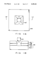
- FIG. 7 is a sectional view showing a structure of a main part of an electronic parts mount device according to Embodiment 3;
- FIG. 8 is a sectional view showing the first modification of the electronic parts mount device shown in FIG. 7;
- FIG. 9 is a sectional view showing the second modification of the electronic parts mount device shown in FIG. 7;
- FIG. 10A is a plan view showing a structure of a main part of an electronic parts mount device according to Embodiment 4.
- FIG. 10B is a sectional view taken along the line 10B--10B of FIG. 10A;
- FIG. 11A is a plan view showing a structure of a main part of an electronic parts mount device according to Embodiment 5;
- FIG. 11B is a sectional view taken along the line 11B--11B of FIG. 11A;
- FIG. 12A is a schematic view for explaining the function of Embodiment 5.
- FIGS. 12B and 12C are sectional views, respectively, taken along the lines of 12B--12B and 12C--12C of FIG. 12A;
- FIGS. 13A to 13C are schematic views showing cases in which a crystal orientation of a substrate to be bonded is deviated
- FIG. 14A is a plan view showing a structure of a main part of an electronic parts mount device according to Embodiment 6;
- FIG. 14B sectional view taken along the line 14B--14B of 14A;
- FIG. 15 is a sectional view showing a structure of a main part of an electronic parts mount device according to Embodiment 7;
- FIG. 16A is a perspective view and FIGS. 16B and 16C are sectional views showing mounting steps of the electronic parts according to Embodiment 8;
- FIG. 17 is a schematic illustration showing a structure of a main part of an electronic parts mounting apparatus used in Embodiment 9;
- FIG. 18 is a sectional view showing an insertion state of the electronic part according to Embodiment 9;
- FIG. 19 is a sectional view showing an insertion state of an electronic part according to Embodiment 10.
- FIG. 20 a plan view showing an insertion state of an electronic part according to Embodiment 11;
- FIG. 21 is a plan view showing an insertion state of a small electronic part according to Embodiment 11.
- FIG. 22 is a sectional view showing an insertion state of a small electronic part according to Embodiment 12.
- an electronic part will be mainly represented by a laser element.
- the present invention can be practiced with other electronic parts such as a microlens, an optical fiber, and a passive part of an element.
- a substrate is not limited to one having a recessed portion, and an Si substrate, a metal substrate, a ceramic substrate, and the like may be selected in accordance with the applications.
- FIG. 1 is a perspective view showing a structure of a main part of an electronic parts mount device according to Embodiment 1 of the present invention.
- An electronic parts mount device 150 of FIG. 1 is obtained by bonding substrates 100A and 100B through an oxide film 110.
- a recessed portion 200 is formed in a central portion of the substrate 100A, and electrode wirings 120 are formed on any other portion of the substrate 100A excluding the recessed portion.
- Two silicon substrates 100A and 100B are formed by smooth polishing to have predetermined thicknesses, e.g., the substrate 100A has a thickness of 250 ⁇ m and the substrate 100B has a thickness of 200 ⁇ m, and are bonded through the oxide film 110 formed by thermal surface oxidation.
- the mount body 150 obtained by bonding the substrates 100A and 100B is subjected to normal masking and etching steps to form the recessed portion 200 as the element mounting portion.
- normal masking and etching steps to form the recessed portion 200 as the element mounting portion.
- Etching in the direction of the depth is automatically stopped by the oxide film 110. Therefore, the size of the recessed portion 200 is automatically determined by the mask precision, and the depth thereof is automatically determined by the substrate thickness precision. As a result, both the size and depth of the recessed portion 200 can be controlled with high precision.
- the necessary electrode wirings 120 and the like are formed in one surface of the mount body 150, and the resultant substrate is cut into a predetermined size.
- the electronic parts mount device 150 (element mounting substrate) is completed.
- FIGS. 2A and 2B, and 3A and 3B show cases in which the electronic parts mount device 150 formed as described above is utilized as a submount of a semiconductor laser module.
- FIGS. 3A and 3B show a laser array in which four lasers are formed as an array, and a fiber array in which four fibers are formed as an array. The number of lasers or fibers constituting the array can be one or more.
- FIGS. 2A and 2B show the steps of mounting a laser element 300 on the electronic parts mount device 150.
- the oxide film 110 exposed to the bottom surface of the recessed portion 200 is removed by hydrofluoric acid or the like.
- a solder member e.g., AuSn
- AuCr a solder member formed on the bottom surface of the recessed portion 200, and the lower surface of the substrate is metallized (e.g., AuCr).
- the mount body 150 is cut out at a predetermined position into a predetermined size (e.g., 3.9 mm ⁇ 6.0 mm).
- the laser element 300 polished to have a predetermined thickness e.g., 100 ⁇ m is mounted on the bottom surface of the recessed portion 200. In this step, if the size of the recessed portion 200 is set to coincide with the size of the laser element 300 and the laser element 300 is mounted such that its edge and the edge of the recessed portion 200 coincide or are parallel to each other, the laser element 300 is accurately arranged.
- the laser element 300 is fixed by soldering in the annealing step and the like.
- the electronic parts mount device 150 of this embodiment is of a submount element type in which an element is mounted, the electronic parts mount device 150 is larger than the laser element 300 itself, and necessary electrode wiring is completed. Therefore, flexibility in handling and the degree of flexibility in mount wiring become large.
- the silicon substrate 100 is used not only as an alignment tool. Rather, as shown in FIG. 2B, when the IC element 300 and the like are formed in the silicon substrate 100 to provide a hybrid IC, the entire module can be reduced in size, and the electrode wirings can be reduced to a minimum. Therefore, it is advantageous especially in a high-speed operation.
- FIGS. 3A and 3B A case in which the submount described above is connected to an optical fiber will be described with reference to FIGS. 3A and 3B.
- a ribbon fiber connector which is a so-called MT connector, is commercially available as a tool for connecting a ribbon fiber in which a plurality of optical fibers are bundled.
- FIG. 3A with an MT connector, two connectors 400 are connected through two pins 440.
- An end face 450 of a ribbon fiber (not shown) inserted from the rear surface of a connector 400 is arranged with high precision between pin insertion portions on the front surface of the connector 400.
- the ribbon fiber can be easily connected to the submount.
- FIG. 3A shows the structure of the MT connector
- FIG. 3B is a sectional view of a completed assembly taken along the line 3B--3B of FIG. 3A.
- the electronic parts mount device is mounted in the MT connector in the following steps.
- the electronic parts mount device 150 is cut out to coincide with the gap (e.g., 3.9 mm) between the pins 440 of each MT connector 400, and is mounted to coincide with a front end 430a of a copper base 430, or is mounted and set back from the front end 430a of the copper base 430 while being parallel to it.
- the lower surface of the electronic parts mount device 150 may be metallized by In vapor deposition and heated to about 200° C. under an appropriate pressure.
- the laser element 300 is arranged at the central portion of the front edge of the electronic parts mount device 150.
- the pins 440 of the MT connectors 400 are fitted to sandwich the electronic parts mount device 150, and the pins 440 are pressed by an appropriate cover 410.
- the cover 410 may press the base 430 by screwing but not by the pins 440.
- the diameter of a pin 440 is generally 700 ⁇ m. If the thickness of the electronic parts mount device 150 is set to 450 ⁇ m, the cover 410 can reliably press the pins 440 without contacting the electronic parts mount device 150. If the thickness of the laser element 300 is set to 100 ⁇ m and that of the bottom portion of the submount is set to 250 ⁇ m, the active layer of the laser element 300 coincides with the height of the central portion of the pins 440, i.e., the central height of the fiber end face 450. As a result, the laser element 300 can be reliably caused to oppose the fiber end face 450.
- the force to urge the MT connectors 400 against the base 430 in the horizontal direction can be obtained by utilizing the clip 460. That is, if the length of the cover 410 is equal to that of the MT connectors 400, the clip 460 only need be fitted. If an appropriate step is formed in the rear portion of the base 430, a holder plate 420 is inserted in this step, and the entire assembly is sandwiched by the clip 460 together with the holder plate 420, the MT connectors 400 can be urged more reliably.
- the above mechanism will be summarized as follows.
- the MT connectors 400 are reliably held at accurate positions with respect to the electronic parts mount device 150, in the lateral direction by sandwiching the electronic parts mount device 150 by the pins 440, in the vertical direction by sandwiching the pins 440 by the cover 410 and the base 430, and in the forward-backward direction by sandwiching by the clip 460.
- the laser electrode element 300 is accurately positioned on the electronic parts mount device 150 as described previously. As a result, the positional relationship between the laser element 300 and the end face 450 of the fiber can be correctly maintained.
- FIG. 4 is a perspective view showing a substrate and an element which have a structure similar to FIG. 2A. Coordinate axes are added in FIG. 4 for the purpose of descriptive convenience of this embodiment.
- a semiconductor element 300 is aligned by side surfaces of a recessed portion 200, in the same manner as in Embodiment 1. Therefore, the semiconductor element 300 is mounted at an accurate position and in accurate directions in any of the X-, Y-, and Z-axes in a mount body 150.
- Si has a high thermal conductivity and a high electric conductivity, no problem arises in terms of heat dissipation and formation of electrodes.
- the mount body 150 has wirings 120 connected to the semiconductor element 300 through bonding wires or the like, and an inclined surface (side surface tapered portion) 210 of the recessed portion 200.
- FIG. 5A is a sectional view taken along a direction of the X-axis of FIG. 4 and shows a state in which the semiconductor element 300, e.g., a semiconductor laser, is fitted in the recessed portion 200 of the mount body 150 shown FIG. 4.
- the semiconductor element 300 e.g., a semiconductor laser
- FIG. 5A shows a state in which the semiconductor element 300, e.g., a semiconductor laser, is fitted in the recessed portion 200 of the mount body 150 shown FIG. 4.
- a fluid member 500 is inserted to fill the space between the element 300 and side surfaces 210 X1 and 210 X2 , the element 300 is held at a correct position between the two side surfaces 210 due to the surface tension of the fluid member 500.
- a pressure is applied to the element 300 from the above, and a solder member 510 formed on the lower surface of the element 300 and the bottom surface of the recessed portion 200 are melted by heating to perform bonding.
- the fluid member 500 to be inserted may be a liquid such as water or alcohol and may be evaporated after alignment. Also, in view of element passivation, it is effective to use a hardening resin or the like as the fluid member 500 to constantly fill the clearances. Furthermore, when a molten low-melting metal or a conductive resin is used, the contact resistance is decreased both electrically and thermally, and thus a more effective result can be obtained.
- the low-melting metal it can be melted in a crucible and is filled in the clearances, or can be filled in the clearances by means of shot or powder filling and then melted by heating.
- a low-melting metal e.g., In or AuSn
- a side surface 210 Y2 facing upward may be provided to oppose a side surface 210 Y1 .
- a notched side surface 210 Z may be formed under the element 300.
- the fluid can be inserted most easily by the following manner. That is, as shown in FIG. 6, a plurality of grooves 250 may be formed in the bottom surface of the recessed portion 200 of the mount body 150, and the fluid may be filled from the side of the side surface 210 Z through an aligning plate 470. In this case, it is possible to form a groove in the aligning plate 470 so that the excessive fluid is discharged through this groove.
- the member 500 inserted between the semiconductor element 300 and the side surface 210 of the recessed portion 200 has a predetermined surface tension, it draws the semiconductor element 300 to the side surface 210. Therefore, if the side surface 210 is formed at a predetermined position, the semiconductor element 300 is self-aligned with respect to the side surface 210.
- FIGS. 7 to 9 are sectional views respectively showing structures of main parts of electronic parts mount devices according to Embodiment 3.
- the same reference numerals in FIGS. 7 to 9 denote the same or corresponding members as in FIGS. 2A and 2B.
- the electronic parts mount device of FIG. 7 is different from that of Embodiment 1 in that a plurality of recessed portions 200 are formed.
- electronic elements 310 such as FETs can be mounted on a substrate 100 similarly to Embodiment 1.
- An oxide film 110 serves as an electrical insulating film between a substrate 100A and the electronic elements 310 when it is left, and can be utilized as part of wirings to ground and the like when it is removed.
- each element can be performed by wire bonding or by TAB connection.
- TAB connection is more preferable. It is because since each electronic element is mounted at a precise position in a mount body 150 and thus collective connection is possible, the process can be simplified with TAB connection. In this case, it is preferable that the height of each electronic element 310 and the depth of the corresponding recessed portion 200 coincide with each other. Then, the effect of the present invention that accurate control of the depth of the recessed portion is facilitated can be sufficiently utilized.
- Embodiments 1 to 3 positioning of a semiconductor element and the like is performed in the bottom portion of the recessed portion 200. It is preferable that the bottom portion of the recessed portion 200 and a contact portion for positioning are at different levels to form a step of a certain degree.
- Embodiments 4 to 7 exemplify a positioning mechanism in which a recessed portion has a double step and a bottom portion and a positioning contact portion of the recessed portion 200 form a step of a certain degree.
- FIGS. 10A and 10B are views showing a structure of a main part of an electronic parts mount device according to Embodiment 4 in which FIG. 10A is a plan view thereof, and FIG. 10B is a sectional view taken along the line 10B--10B of FIG. 10A.
- a positioning recessed portion has a double step, and only a peripheral portion of the recessed portion of Embodiments 1 to 3 is shown.
- silicon substrates 100A, 100B, and 100C are bonded to each other through SiO 2 films 110A and 100B.
- An Si 3 N 4 film 115 is deposited on the lower surface of the uppermost silicon substrate 100C.
- those of the silicon substrates 100A, 100B, and 100C may be set to 250 ⁇ m, 10 ⁇ m, and 190 ⁇ m, respectively, those of the SiO 2 films 110A and 110B may be set to 1 ⁇ m, and that of the Si 3 N 4 film 115 may be set to 0.2 ⁇ m.
- the respective substrates can be formed by combining the steps of thermal oxidation, direct bonding, polishing, CVD, and the like.
- the uppermost silicon substrate 100C is etched by normal photolithography in the same manner as in the embodiments described above.
- the crystal orientation of the silicon is formed such that the silicon substrates 100A, 100B, and 100C are bonded respectively with ⁇ 1 0 0 ⁇ planes and the mask pattern has ⁇ 0 1 1> and ⁇ 0 1 -1> directions.
- anisotropic chemical etching using a KOH aqueous solution or the like may be performed.
- the Si 3 N 4 film 115 exposed by etching is removed by ion milling, dry etching, or the like.
- the SiO 2 film 110B sandwiched between the Si 3 N 4 film 115 and the silicon substrate 100B is etched by selective side etching of, e.g., 10 ⁇ m by using an aqueous solution of ammonium fluoride or the like.
- silicon anisotropic chemical etching is performed again to form a recessed portion having a double step, as shown in FIG. 10B, and positioning of the semiconductor element 310 can be effectively performed.
- the pattern for the silicon substrate 100C and that for the silicon substrate 100B can be formed by self-alignment. Therefore, no pattern offset occurs between the two substrates 100B and 100C, and a problem due to double step does not occur.
- FIGS. 11A and 11B show Embodiment 5 of the present invention, in which FIG. 11A is a plan view thereof, and FIG. 11B is a sectional view taken along the line 11B--11B of FIG. 11A.
- FIG. 11A is a plan view thereof
- FIG. 11B is a sectional view taken along the line 11B--11B of FIG. 11A.
- silicon substrates 100A, 100B, and 100C are bonded through only SiO 2 films 110A and 110B, the silicon substrates 100B and 100C are directly bonded by changing the crystal planes or crystal orientations.
- the silicon substrate 100B on the silicon substrate 100A (having an arbitrary crystal orientation) is bonded with a ⁇ 1 1 0 ⁇ plane, and the silicon substrate 100C is bonded with a ⁇ 1 0 0 ⁇ plane. Also, a ⁇ 0 0 1> direction of the silicon substrate 100B is aligned with a ⁇ 0 1 1> direction of the silicon substrate 100C.
- a mask pattern having ⁇ 0 1 1> and ⁇ 0 1 -1> directions is formed on the surface of the silicon substrate 100C of the mount body 150, and anisotropic chemical etching of silicon is performed in the same manner as in the case of FIGS. 10A and 10B. Subsequently, the exposed portion of the SiO 2 film 110B is removed by etching, and anisotropic chemical etching of silicon is performed again. As a result, each silicon crystal exhibits a geometric ⁇ 1 1 1 ⁇ crystal plane matching the shape of the mask. Especially, an intermediate portion 110B' of the silicon substrate 100B is etched to form a rhombus or parallelogram inscribing the mask pattern. The pattern of a rhombus or parallelogram can be formed such that most of its side surface forms a vertical surface by appropriately setting the thickness of the silicon substrate 100B.
- FIG. 12A shows only a square pattern (solid line) serving as a mask and an etching pattern (broken line)
- FIG. 12B is a sectional view taken along the line 12B--12B of FIG. 12A
- FIG. 12C is a sectional view taken along the line 12C--12C of FIG. 12A.
- 12A to 12C show an opening for positioning, i.e., a positioning pattern 220 of a semiconductor element or the like, a region 210A to which the SiO 2 film 110A on the bottom portion is exposed in an etched region (having a vertical surface on the boundary side surface) of the silicon substrate 100B, and a region 210B to which the SiO 2 film 110A on the bottom portion is not exposed.
- the region 210B has an inclined surface, as shown in FIG. 12B, and this inclined surface is a ⁇ 1 1 1 ⁇ (equivalent to a (1 1 1) plane) plane which is the same as the vertical surface of the boundary of the rhombus.
- the inclined surface 210B can be further extended if the silicon substrate 110B is sufficiently thick, it is stopped in FIG. 12B at an indicated position since the extending amount (depth) is defined by the SiO 2 film 110A. If the region 210B is extended to the opening 220, the initial object cannot be achieved as the bottom surface of the opening does not become flat. Therefore, these portions must be designed by considering the dimensional relationship among the size of the opening 220, the thickness of the silicon substrate 100B, and the size of the inclined surface 210B.
- the opening 220 serving as the mask is a square having a side with a length a, and the vertical diagonal of the rhombus of FIG. 12A is in the ⁇ 0 0 1> direction of the silicon substrate 100B.
- the thickness of the silicon substrate 100B is defined as D
- b, c, and d are defined as shown in FIG. 12A.
- FIGS. 14A and 14B show Embodiment 6, in which FIG. 14A is a plan view thereof, and FIG. 14B is a sectional view taken along the line 14B--14B of FIG. 14A.
- silicon substrates 100A, 100B, and 100C are bonded through only SiO 2 films 110A and 110B, in the same manner as in FIGS. 11A and 11B.
- Bonding is performed such that both the silicon substrates 100B and 100C on the single substrate 100A (having an arbitrary crystal orientation) are set to have (1 0 0 ⁇ planes and the ⁇ 0 1 1> direction of the silicon substrate 100B and the ⁇ 0 1 1> direction of the silicon substrate 100C are deviated from each other, e.g., by 45°.
- a mask pattern extending in the ⁇ 0 1 1> and ⁇ 0 1 -1> directions is formed on the surface of the silicon substrate 100C, in the same manner as in the case of FIGS. 11A and 11B.
- Anisotropic chemical etching of silicon is performed, and the exposed SiO 2 film 110B is removed by etching. Subsequently, anisotropic chemical etching of silicon is performed again.
- both the silicon substrates 100B and 100C have a geometric ⁇ 1 1 1 ⁇ crystal plane matching the shape of the mask.
- an intermediate portion 100B' of the silicon substrate 100B is etched to form a square or rectangle inscribed by a pattern serving as a mask.
- the square or rectangular pattern has a side surface of a ⁇ 1 1 1 ⁇ plane, and its corner portions do not form a flat bottom surface with respect to the square or rectangular mask opening. Even so, this irregular mask can be used to achieve the object, and further can also be applied as a holder of a lens 350 as shown in FIG. 14B.
- FIGS. 14A and 14B can be applied to a surface input/output type electronic parts mount device.
- FIG. 15 shows Embodiment 7. Silicon substrates 100B and 100C are bonded through an SiO 2 film 110B. Bonding is performed such that both the silicon substrates 100B and 100C have a ⁇ 1 0 0 ⁇ plane and the ⁇ 0 1 1> direction of the silicon substrate 100B and the ⁇ 0 1 1> direction of the silicon substrate 100C are deviated from each other, e.g., by 45°. A protection mask such as SiO 2 is formed on the lower surface of the silicon substrate 100B.
- a mask pattern extending in the ⁇ 0 1 1> and ⁇ 0 1 -1> directions is formed on the upper surface of the silicon substrate 100C, in the same manner as in the case of FIGS. 11A and 11B.
- Anisotropic chemical etching of silicon is performed, the exposed SiO 2 film is removed by etching, and subsequently, anisotropic etching of silicon is performed again.
- both the silicon substrates 100B and 100C have a geometric ⁇ 1 1 1 ⁇ crystal plane matching the shape of the mask.
- the intermediate portion 100B' of the silicon substrate 100B is etched to form a square or rectangle inscribed by a pattern serving as a mask. Thereafter, the protection mask on the lower surface of the silicon substrate 100B is removed, and the surface input/output type semiconductor element (e.g., a semiconductor laser, a light-emitting diode, or a photodiode) 310 and the lens 350 are mounted and electrically connected.
- the surface input/output type semiconductor element e.g., a semiconductor laser, a light-emitting diode, or a photodiode
- Embodiments 1 to 7 exemplify positioning by using the recessed portion of the substrate. Positioning can also be performed without forming a recessed portion in the substrate but through a metal bump.
- FIGS. 16A, 16B, and 16C show a process for explaining the method of Embodiment of the present invention.
- a solder member 510 is formed on a lower electrode 540 of an element 300 by using a pattern, and bumps 530 are formed in part of the region of the solder member 510. Same patterning and bump formation are performed for a substrate 100.
- the opposing bumps 530 are bonded to each other, and the element 300 is heated in a free state. In this step, the element 300 is automatically moved by the metal centering effect to a position to which it should be connected.
- the crushed bumps 530 can spread on the entire lower surface of the element 300, so that the bumps 530 also serve as the solder members.
- An insulating film can be formed on the bumps or the solder member to obtain electrical insulation, depending on the case.
- the positions of the bumps 530 are not limited to the four corners of the element 300.
- the bumps can be formed on the electrode of the upper surface of the element 300, but not on the electrode on the lower surface of the element 300, and flip chip connection can be performed in a face-down state. By this embodiment, the opposing electrodes are automatically aligned. Therefore, a small electrode pattern, that cannot be achieved by conventional flip chip connection, can be formed on the surface of the element.
- the method of this embodiment can be applied not only to a flat substrate but also to a bottom surface having a hole as described in FIG. 4, and can also be combined with the method of Embodiment 2.
- the number of side surfaces to be positioned can be one depending on the case, and the side surfaces need not intersect at a right angle.
- the method of Embodiment 8 when the semiconductor element is bonded through the metal bumps and then heated, the element is automatically positioned with respect to the substrate by the metal bump centering effect described previously. By any method, the element is bonded in tight contact with the flat surface. Therefore, heat generated by the element is easily dissipated.
- Embodiments 1 to 8 utilize the metal centering effect.
- Embodiments 9 to 12 show a method for correctly positioning an electronic part by utilizing a small vibration.
- FIG. 17 is a schematic view showing an apparatus for mounting electronic parts according to Embodiment 9 of the present invention.
- a small vibration is given from a side portion of a substrate.
- the small vibration can be given not only from the side surface but also from other surfaces such as an upper or lower surface.
- a recessed portion 200 is formed in an upper surface of a substrate 100 comprising an Si substrate by dry etching.
- a movable support member 600 supports a semiconductor element 300 (electronic part to be mounted in the recessed portion 200 and moves toward the substrate 100.
- the movable support member 600 can be obtained by, e.g., mounting a vacuum chuck capillary on a movable mechanism.
- a heater (not shown) is mounted in a support base 610 for placing the substrate 100, in order to heat the substrate 100.
- a support section 620 for supporting the substrate 100 in the lateral direction has a press mechanism using, e.g., a spring.
- a small vibration generator 630 gives a small vibration to the substrate 100 through the support section 620.
- the small vibration generator 630 is constituted by a vibrator comprising an electromagnet and an iron piece, or a electroacoustic converter, e.g., a piezoelectric transducer or a ferrite vibrating element.
- the apparatus of this embodiment further comprises an AC generator 640 for driving the small vibration generator 630, and a stationary wall 650.
- the substrate 100 is mounted on the support base 610 and supported by the support section 620.
- the substrate 100 can be supported not only by the method shown in FIG. 17 but also by upward pressing, vacuum chucking from the lower surface, or a combination of them.
- the electronic part 300 is transferred to the recessed portion 200 in the substrate 100 by the movable support member 600.
- the AC generator 640 is operated to give a small vibration to the substrate 100 so that the electronic part 300 is inserted in the substrate 100.
- two different methods are available. That is, according to the first method, the electronic part 300 is inserted while being chucked (supported) by the movable support mechanism 600. According to the second method, the electronic part 300 is preliminarily placed in or in the vicinity of the recessed portion 200 and chucking (supporting) by the movable support member 600 is released.
- the electronic part 300 such as a semiconductor element tends to be easily broken, when a small vibration is given to it, its end portion or its contacting portion with the movable support member 600 can be damaged.
- the electronic part 300 is not inserted in the recessed portion 200 but slidably moves on the substrate 100 in a rare case, it is not likely to be damaged.
- the AC generator 640 is stopped, or the AC generator 640 is kept operating depending on the case, and a pressure is applied to the electronic part 300 by the movable support member 600 or by a separate pressure applying mechanism.
- the solder member is melted by the heater of the support base 610 and then is cooled and solidified to fix the electronic part 300.
- the electronic part 300 can be fixed by any other method than soldering.
- a thermosetting resin or ultraviolet-curing resin may be used and thermal hardening or ultraviolet-light curing may be caused.
- FIG. 18 is a sectional view and shows a state in which a semiconductor element 300 is inserted by using the apparatus and method shown in FIG. 17.
- a semiconductor element e.g., a semiconductor laser element
- a substrate 100 is an n-type low-resistance Si substrate.
- a multilayer film mask of SiO 2 and Si 3 N 4 is formed on the Si substrate 100. Dry etching (about 50 ⁇ m) using a CF 4 +O 2 gas is performed to form a recessed portion 200 (holder portion).
- the mask size was determined so that the recessed portion 200 had a size of 305 ⁇ m ⁇ 405 ⁇ m at its semiconductor element inserting portion.
- a GaInAsP/InP type semiconductor laser element was employed and cut out by a scriber to form the semiconductor element 300 having a thickness of about 100 ⁇ m and a size of 300 ⁇ m ⁇ 400 ⁇ m, while leaving clearances with respect to the recessed portion 200 of about 5 ⁇ m each.
- Multilayer vapor deposition was performed to deposit Au, Sn, and Au (Sn was about 20%) in the recessed portion 200 of the substrate 100 to a thickness of about 2 ⁇ m in accordance with the lift-off method.
- the formed multilayer was a solder member 510 for fixing the semiconductor element.
- the semiconductor element 300 was placed upside up on the substrate 100 fabricated in this manner Most part of the semiconductor element 300 was incompletely inserted, as indicated by a broken line 300' in FIG. 18. Thereafter, a small vibration is applied to the substrate 100 while chucking of the semiconductor element 300 was released. Then, most part of the semiconductor element 300 was correctly inserted, as indicated by a solid line in FIG. 18.
- the small vibration applied in this case has a frequency of 50 Hz and an amplitude of about 2 ⁇ m.
- the insertion state was not largely changed even when the frequency of vibration was changed, and a correct insertion state was obtained at substantially any frequency. It was found that an incomplete insertion was due to an incomplete shape of the semiconductor element 300 obtained by cutting.
- the small vibration can be of a high-frequency range. Especially, if a so-called ultrasonic vibration of 20 kHz or more is employed, it is above a human audible level. Therefore, a machine noise trouble caused by a small mechanical vibration, i.e., audible discomfort to a person operating the apparatus is substantially prevented, and a silencer or noise control equipment is not needed at a site where the apparatus is installed. If the amplitude of the small vibration is 10 ⁇ m or less, adverse effects to the person operating the apparatus and a surrounding apparatus can be suppressed. As a small vibration in the ultrasonic range, e.g., a vibration having a frequency of 60 kHz and an amplitude of about 1 ⁇ m was applied.
- the obtained insertion state was as good as that described previously.
- the direction of vibration, the vibration propagation state, the vibration waveform, and the like of these small vibrations can be arbitrarily set, and may be appropriately selected in accordance with the frequency of vibration, amplitude, or variations in them over time, as well as the material and the shape of the substrate and the electronic part employed.
- the resultant structure was heated to about 350° C. in a nitrogen atmosphere containing a 20% hydrogen while pressing the element with a load of about 10g, thereby fixing the semiconductor element by the solder member 510.
- the alignment state of the semiconductor element was as follows. That is, excluding a defective element having a smaller size due to inappropriate cutting, the center of the semiconductor element was aligned with the center of the holder portion of the substrate in any direction with an error of about ⁇ 2 ⁇ m. According to the result of the proper test of the packaged semiconductor laser element, characteristics as good as those before mounting were obtained.
- the electronic part 300 is transferred to the recessed portion 200 in the substrate 100, and a small vibration is applied to the substrate 100 by the small vibration generator 630. Therefore, the electronic part 300 can be correctly arranged in the recessed portion 200, as indicated by the solid line in FIG. 18, without causing an inclination error as indicated by the broken line in FIG. 18. As a result, the clearance in the recessed portion can be reduced in size, and the alignment precision can be improved, thus improving the productivity.
- FIG. 19 is a view for explaining Embodiment 10 of the present invention.
- FIG. 19 is a sectional view showing a recessed portion 200, for receiving a semiconductor element 300, formed in a tapered manner.
- This embodiment is advantageous in the following respects. That is, since the opening of the recessed portion 200 is widened, preliminary mounting of the semiconductor element 300 is facilitated. Also, since the recessed portion 200 has a tapered shape, movement of the semiconductor element 300 to the bottom portion of the recessed portion 200 by application of a small vibration is facilitated. Since a clearance becomes narrow only at the bottom portion of the recessed portion 200, when a solder is melted by heating, upward warp of the solder to the side surface of the semiconductor element due to the capillary of the solder member can be prevented.
- the substrate 100 comprises Si substrates 100A and 100B, and an SiO 2 film 110.
- This structure is needed because of the following reason.
- the size (processing precision) of the bottom portion of the recessed portion is determined by the precision of the processing depth. Therefore, to form a recessed portion having a deep clearance, the processing depth need be precisely controlled.
- a so-called direct bonding method can be used. More specifically, the two Si substrates 100A and 100B subjected to mirror surface polishing and cleaning are brought into contact with each other and are heated at a high temperature to perform direct bonding at an atomic level. With this method, a substrate including the substrate 100A of a thickness of 250 ⁇ m, the SiO 2 film 110 of a thickness of 2 ⁇ m, and the substrate 100B of a thickness of 200 ⁇ m is formed.
- the Si substrate surface is set to have a (1 0 0) plane, the recessed portion 200 is set to be aligned with the ⁇ 0 1 1> and ⁇ 0 1 1> directions, and an SiO 2 mask (window) having a size of 595 ⁇ m ⁇ 695 ⁇ m is formed. Thereafter, chemical etching is performed using an aqueous solution of KOH of a temperature of 80° to 90° C. to expose the SiO 2 film 110. Subsequently, the SiO 2 film 110 is chemically etched using a solution of ammonium fluoride. In this manner, the substrate 100 with the recessed portion 200 of the bottom portion size of 305 ⁇ m ⁇ 405 ⁇ m and a tapered angle of about 54° can be formed.
- the SiO 2 film 110 as the intermediate layer can be selectively stepped back, i.e., selectively etched. If the SiO 2 film 110 is appropriately overreached, it can be utilized as a solder amount adjusting mechanism for absorbing an excessive solder.
- FIG. 20 is a view for describing Embodiment 11 of the present invention, and is a plan view showing a recessed portion in which a semiconductor element is to be inserted.
- This embodiment is an improved embodiment for the purpose of mounting of a semiconductor element and the like.
- an electronic part 300 e.g., a semiconductor element
- a method of, e.g., scribing or dicing described previously is obtained by cutting in accordance with a method of, e.g., scribing or dicing described previously.
- an intermediate surface portion obtained during cutting is formed comparatively smooth.
- a so-called burr or local deformation can be formed at a boundary during cutting, e.g., a corner of the semiconductor element 300. Such deformation often becomes an obstacle as defective shape when a high alignment precision of several ⁇ m is required.
- narrow portions of the clearance are formed to avoid the corners of the semiconductor element 300. That is, portions of the recessed portion 200 corresponding to the four corners of the semiconductor element 300 are formed to spread outwardly, so that defective insertion or defective alignment of the semiconductor element 300 is suppressed.
- the above problem can also be effectively avoided by forming narrow portions of the clearance in the form of a plurality of point contacts, as shown in FIG. 21.
- the clearance of the holder portion of the substrate opposing the electronic part to be mounted is significant, and when the clearance is large, the alignment precision tends to be easily degraded.
- the clearance between the electronic part and the recessed portion of the substrate is 10 ⁇ m or less. With the clearance of this size, an alignment error becomes ⁇ 5 ⁇ m or less. Then, the present invention can be applied to alignment between a single mode optical fiber and a light-emitting element.
- FIG. 22 is a view for describing Embodiment 12 of the present invention, and is a sectional view of a recessed portion, for receiving a semiconductor element, formed in a tapered manner.
- a positioning jig is auxiliarily used for inserting the electronic part.
- the self-alignment effect is enhanced without greatly reducing the clearance used for alignment.
- the clearance can be set sufficiently large. Therefore, even when a metal substrate and a glass lens are to be assembled, temperature dependency (e.g., a change in characteristic due to a variation in optical axis) caused by contact between the electronic part and the substrate can be suppressed.
- a positioning jig 700 shown in FIG. 22 is formed of silicon by, e.g., etching, and its size and shape are determined such that it contacts the inner surface of a recessed portion 200 of a mount body 150 and the outer surface of an electronic part 300.
- the electronic part 300 is preliminarily mounted.
- the positioning jig 700 is placed on the electronic part 300, and a small vibration is applied to the small electronic part 300 through the jig 700, thereby achieving predetermined positioning. If a chuck hole 710 for vacuum chucking is formed in the positioning jig 700, both the positioning jig 700 and the electronic part 300 can be supported and moved at once.
- the clearance is preferably designed to be large considering the machining limit and strength of the positioning jig 700. Hence, the clearance need to be 10 ⁇ m or larger.
- the substrates bonded to provide the mount body 150 are not limited to a combination of silicon substrates, but various combinations, e.g., silicon and Ge, silicon and GaAs, silicon and InP, silicon and InSb, and the like are possible.
- the substrate to be bonded is not limited to a semiconductor material, but a dielectric substrate can also be used.
- Al 2 O 3 , AlN, C-Bn, a ceramic material such as SiC, or a polymer material such as a polyimide can be used.
- a part to be mounted in the recessed portion is not limited to an optical element or an electronic element, but a fiber, a pin, or a screw can be fitted in the recessed portion and positioned.
- a semiconductor element to be mounted in the recessed portion is not limited to a semiconductor laser element, but various types of other semiconductor elements that need precise mechanical alignment can be mounted according to the present invention.
- the part to be mounted is not limited to a semiconductor element, but various types of other electronic parts such as an optical element can be mounted according to the present invention.
- a small vibration is applied to the substrate.
- a small vibration can be applied only to the electronic part, or to both of them.
- a recessed portion is formed in a mount body, obtained by directly bonding a plurality of substrates, to reach a substrate bonding portion, and a semiconductor element is mounted in the recessed portion. Therefore, a positional relationship between the semiconductor element and other module constituent parts can be correctly held, and the semiconductor element can be mechanically firmly supported.
Abstract
Description
Claims (18)
Applications Claiming Priority (6)
| Application Number | Priority Date | Filing Date | Title |
|---|---|---|---|
| JP2-259036 | 1990-09-28 | ||
| JP25903690 | 1990-09-28 | ||
| JP3-162821 | 1991-07-03 | ||
| JP16282191 | 1991-07-03 | ||
| JP21184691 | 1991-08-23 | ||
| JP3-211846 | 1991-08-23 |
Publications (1)
| Publication Number | Publication Date |
|---|---|
| US5205032A true US5205032A (en) | 1993-04-27 |
Family
ID=27322062
Family Applications (1)
| Application Number | Title | Priority Date | Filing Date |
|---|---|---|---|
| US07/766,204 Expired - Lifetime US5205032A (en) | 1990-09-28 | 1991-09-27 | Electronic parts mounting apparatus |
Country Status (1)
| Country | Link |
|---|---|
| US (1) | US5205032A (en) |
Cited By (48)
| Publication number | Priority date | Publication date | Assignee | Title |
|---|---|---|---|---|
| US5384689A (en) * | 1993-12-20 | 1995-01-24 | Shen; Ming-Tung | Integrated circuit chip including superimposed upper and lower printed circuit boards |
| US5412748A (en) * | 1992-12-04 | 1995-05-02 | Kabushiki Kaisha Toshiba | Optical semiconductor module |
| GB2286485A (en) * | 1994-02-15 | 1995-08-16 | Ibm | Alignment apparatus and method |
| US5523641A (en) * | 1992-05-27 | 1996-06-04 | Nihon Musen Kabushiki Kaisha | Surface acoustic wave device |
| WO1998020545A1 (en) * | 1996-11-08 | 1998-05-14 | W.L. Gore & Associates, Inc. | Method for manufacturing high tolerance cavities in chip packages |
| WO1998020546A1 (en) * | 1996-11-08 | 1998-05-14 | W.L. Gore & Associates, Inc. | High tolerance cavities in chip packages |
| US5895554A (en) * | 1997-02-21 | 1999-04-20 | Gordon; Thomas A. | Alignment method and apparatus for mounting electronic components |
| US5898992A (en) * | 1996-04-30 | 1999-05-04 | Pressac Limited | Method of mounting circuit components on a flexible substrate |
| US6000127A (en) * | 1996-08-08 | 1999-12-14 | Matsushita Electric Industrial Co., Ltd. | Electronic parts mounting method |
| US6161748A (en) * | 1995-05-19 | 2000-12-19 | Hitachi, Ltd. | Process for manufacturing electronic circuits |
| EP1122567A1 (en) * | 2000-02-02 | 2001-08-08 | Corning Incorporated | Passive alignement using slanted wall pedestal |
| US6304185B1 (en) | 1999-08-12 | 2001-10-16 | Micron Technology, Inc. | Devices for sensing living organisms, devices for sensing termites, methods of forming devices for sensing termites, and methods for sensing termites |
| US6313748B1 (en) | 1999-08-27 | 2001-11-06 | Micron Technology, Inc. | Electrical apparatuses, termite sensing apparatuses, methods of forming electrical apparatuses, and methods of sensing termites |
| US6323772B1 (en) | 1999-08-12 | 2001-11-27 | Micron Technology, Inc. | Devices for sensing termites and other living organisms, and methods of forming devices for sensing termites |
| US6366468B1 (en) * | 2000-04-28 | 2002-04-02 | Hewlett-Packard Company | Self-aligned common carrier |
| US6373391B1 (en) | 1999-08-12 | 2002-04-16 | Micron Technology, Inc. | Devices for sensing changes in environments proximate the devices, devices for sensing termites, and methods for sensing termites |
| US6392545B2 (en) * | 1999-08-27 | 2002-05-21 | Micron Technology, Inc. | Electrical apparatuses, and methods of forming electrical apparatuses |
| WO2002067291A2 (en) * | 2001-02-20 | 2002-08-29 | Infineon Technologies Ag | Arrangement of a semi-conductor chip on a substrate |
| US20030198454A1 (en) * | 2002-04-19 | 2003-10-23 | Ritek Corporation | Fiber array module fabrication method and apparatus therefor |
| US20040183182A1 (en) * | 2002-01-23 | 2004-09-23 | Susan Swindlehurst | Apparatus incorporating small-feature-size and large-feature-size components and method for making same |
| US20040188531A1 (en) * | 2003-03-24 | 2004-09-30 | Gengel Glenn W. | RFID tags and processes for producing RFID tags |
| US20040200882A1 (en) * | 2001-07-23 | 2004-10-14 | Slater David B. | Bonding of light emitting diodes having shaped substrates |
| US6809936B2 (en) * | 2002-02-07 | 2004-10-26 | E.Pak International, Inc. | Integrated circuit component carrier with angled supporting and retaining surfaces |
| US20050270757A1 (en) * | 2001-05-31 | 2005-12-08 | Credelle Thomas L | Electronic devices with small functional elements supported on a carrier |
| US20060109123A1 (en) * | 2004-11-22 | 2006-05-25 | Curt Carrender | Radio frequency identification (RFID) tag for an item having a conductive layer included or attached |
| US20060109129A1 (en) * | 2004-11-22 | 2006-05-25 | Curt Carrender | Transponder incorporated into an electronic device |
| US20060109130A1 (en) * | 2004-11-22 | 2006-05-25 | Hattick John B | Radio frequency identification (RFID) tag for an item having a conductive layer included or attached |
| EP1667511A1 (en) * | 2004-12-02 | 2006-06-07 | Delphi Technologies, Inc. | Method for assembling an electrical device |
| US20060118932A1 (en) * | 2004-11-09 | 2006-06-08 | Kabushiki Kaisha Toshiba | Ultrasonic bonding equipment for manufacturing semiconductor device, semiconductor device and its manufacturing method |
| US20060131709A1 (en) * | 2004-12-21 | 2006-06-22 | Caron Michael R | Semiconductor die positioning system and a method of bonding a semiconductor die to a substrate |
| US20060148166A1 (en) * | 2004-11-08 | 2006-07-06 | Craig Gordon S | Assembly comprising functional devices and method of making same |
| US7183636B1 (en) * | 1999-05-27 | 2007-02-27 | Gemplus | Adapter for a chip card having a reduced format in comparison with the standard SIM mini-card format |
| EP1797540A1 (en) * | 2004-10-05 | 2007-06-20 | Tracking Technologies, Inc. | Radio frequency identification tag and method of making the same |
| US7288432B2 (en) | 1999-03-16 | 2007-10-30 | Alien Technology Corporation | Electronic devices with small functional elements supported on a carrier |
| US7452748B1 (en) | 2004-11-08 | 2008-11-18 | Alien Technology Corporation | Strap assembly comprising functional block deposited therein and method of making same |
| US7542301B1 (en) | 2005-06-22 | 2009-06-02 | Alien Technology Corporation | Creating recessed regions in a substrate and assemblies having such recessed regions |
| US7551141B1 (en) | 2004-11-08 | 2009-06-23 | Alien Technology Corporation | RFID strap capacitively coupled and method of making same |
| CN101814700A (en) * | 2009-02-24 | 2010-08-25 | 索尼公司 | Light-emitting device and manufacture method thereof |
| US20110049334A1 (en) * | 2008-01-16 | 2011-03-03 | Furukawa Electric Co., Ltd. | Optical module |
| US20120115262A1 (en) * | 2010-03-29 | 2012-05-10 | Semprius, Inc. | Laser assisted transfer welding process |
| US20130182401A1 (en) * | 2012-01-12 | 2013-07-18 | Ibiden Co., Ltd. | Wiring board and method for manufacturing the same |
| CN108074907A (en) * | 2016-11-18 | 2018-05-25 | 日月光半导体制造股份有限公司 | Semiconductor substrate comprising built-in module and the method for manufacturing the Semiconductor substrate |
| US10189243B2 (en) | 2011-09-20 | 2019-01-29 | X-Celeprint Limited | Printing transferable components using microstructured elastomeric surfaces with pressure modulated reversible adhesion |
| US10252514B2 (en) | 2014-07-20 | 2019-04-09 | X-Celeprint Limited | Apparatus and methods for micro-transfer-printing |
| US10748793B1 (en) | 2019-02-13 | 2020-08-18 | X Display Company Technology Limited | Printing component arrays with different orientations |
| US10813259B2 (en) | 2015-11-18 | 2020-10-20 | Fuji Corporation | Board work machine and insertion method |
| US10899067B2 (en) | 2015-07-20 | 2021-01-26 | X Display Company Technology Limited | Multi-layer stamp |
| US11062936B1 (en) | 2019-12-19 | 2021-07-13 | X Display Company Technology Limited | Transfer stamps with multiple separate pedestals |
Citations (6)
| Publication number | Priority date | Publication date | Assignee | Title |
|---|---|---|---|---|
| US3520054A (en) * | 1967-11-13 | 1970-07-14 | Mitronics Inc | Method of making multilevel metallized ceramic bodies for semiconductor packages |
| JPS5418692A (en) * | 1977-07-13 | 1979-02-10 | Oki Electric Ind Co Ltd | Light emitting device with reflector |
| US4627161A (en) * | 1983-12-19 | 1986-12-09 | At&T Technologies, Inc. | Method for inserting multilead components into printed wiring boards |
| US4860442A (en) * | 1988-11-28 | 1989-08-29 | Kulite Semiconductor | Methods for mounting components on convoluted three-dimensional structures |
| US4875285A (en) * | 1987-11-10 | 1989-10-24 | Siemens Aktiengesellschaft | Apparatus and method for equipping printed circuit boards with components |
| US5046238A (en) * | 1990-03-15 | 1991-09-10 | Rogers Corporation | Method of manufacturing a multilayer circuit board |
-
1991
- 1991-09-27 US US07/766,204 patent/US5205032A/en not_active Expired - Lifetime
Patent Citations (6)
| Publication number | Priority date | Publication date | Assignee | Title |
|---|---|---|---|---|
| US3520054A (en) * | 1967-11-13 | 1970-07-14 | Mitronics Inc | Method of making multilevel metallized ceramic bodies for semiconductor packages |
| JPS5418692A (en) * | 1977-07-13 | 1979-02-10 | Oki Electric Ind Co Ltd | Light emitting device with reflector |
| US4627161A (en) * | 1983-12-19 | 1986-12-09 | At&T Technologies, Inc. | Method for inserting multilead components into printed wiring boards |
| US4875285A (en) * | 1987-11-10 | 1989-10-24 | Siemens Aktiengesellschaft | Apparatus and method for equipping printed circuit boards with components |
| US4860442A (en) * | 1988-11-28 | 1989-08-29 | Kulite Semiconductor | Methods for mounting components on convoluted three-dimensional structures |
| US5046238A (en) * | 1990-03-15 | 1991-09-10 | Rogers Corporation | Method of manufacturing a multilayer circuit board |
Cited By (94)
| Publication number | Priority date | Publication date | Assignee | Title |
|---|---|---|---|---|
| US5523641A (en) * | 1992-05-27 | 1996-06-04 | Nihon Musen Kabushiki Kaisha | Surface acoustic wave device |
| US5412748A (en) * | 1992-12-04 | 1995-05-02 | Kabushiki Kaisha Toshiba | Optical semiconductor module |
| US5384689A (en) * | 1993-12-20 | 1995-01-24 | Shen; Ming-Tung | Integrated circuit chip including superimposed upper and lower printed circuit boards |
| GB2286485A (en) * | 1994-02-15 | 1995-08-16 | Ibm | Alignment apparatus and method |
| CN100341388C (en) * | 1994-02-15 | 2007-10-03 | 国际商业机器公司 | Device and method for aligning assembly with electric circuit board |
| US6161748A (en) * | 1995-05-19 | 2000-12-19 | Hitachi, Ltd. | Process for manufacturing electronic circuits |
| US5898992A (en) * | 1996-04-30 | 1999-05-04 | Pressac Limited | Method of mounting circuit components on a flexible substrate |
| US6000127A (en) * | 1996-08-08 | 1999-12-14 | Matsushita Electric Industrial Co., Ltd. | Electronic parts mounting method |
| WO1998020546A1 (en) * | 1996-11-08 | 1998-05-14 | W.L. Gore & Associates, Inc. | High tolerance cavities in chip packages |
| WO1998020545A1 (en) * | 1996-11-08 | 1998-05-14 | W.L. Gore & Associates, Inc. | Method for manufacturing high tolerance cavities in chip packages |
| US5895554A (en) * | 1997-02-21 | 1999-04-20 | Gordon; Thomas A. | Alignment method and apparatus for mounting electronic components |
| US7425467B2 (en) | 1999-03-16 | 2008-09-16 | Alien Technology Corporation | Web process interconnect in electronic assemblies |
| US7288432B2 (en) | 1999-03-16 | 2007-10-30 | Alien Technology Corporation | Electronic devices with small functional elements supported on a carrier |
| US7183636B1 (en) * | 1999-05-27 | 2007-02-27 | Gemplus | Adapter for a chip card having a reduced format in comparison with the standard SIM mini-card format |
| US6304185B1 (en) | 1999-08-12 | 2001-10-16 | Micron Technology, Inc. | Devices for sensing living organisms, devices for sensing termites, methods of forming devices for sensing termites, and methods for sensing termites |
| US6323772B1 (en) | 1999-08-12 | 2001-11-27 | Micron Technology, Inc. | Devices for sensing termites and other living organisms, and methods of forming devices for sensing termites |
| US6373391B1 (en) | 1999-08-12 | 2002-04-16 | Micron Technology, Inc. | Devices for sensing changes in environments proximate the devices, devices for sensing termites, and methods for sensing termites |
| US6392545B2 (en) * | 1999-08-27 | 2002-05-21 | Micron Technology, Inc. | Electrical apparatuses, and methods of forming electrical apparatuses |
| US6630887B2 (en) | 1999-08-27 | 2003-10-07 | Micron Technology, Inc. | Electrical apparatuses, and methods of forming electrical apparatuses |
| US6313748B1 (en) | 1999-08-27 | 2001-11-06 | Micron Technology, Inc. | Electrical apparatuses, termite sensing apparatuses, methods of forming electrical apparatuses, and methods of sensing termites |
| EP1122567A1 (en) * | 2000-02-02 | 2001-08-08 | Corning Incorporated | Passive alignement using slanted wall pedestal |
| US6366468B1 (en) * | 2000-04-28 | 2002-04-02 | Hewlett-Packard Company | Self-aligned common carrier |
| WO2002067291A2 (en) * | 2001-02-20 | 2002-08-29 | Infineon Technologies Ag | Arrangement of a semi-conductor chip on a substrate |
| WO2002067291A3 (en) * | 2001-02-20 | 2002-11-14 | Infineon Technologies Ag | Arrangement of a semi-conductor chip on a substrate |
| US20070256291A1 (en) * | 2001-05-31 | 2007-11-08 | Credelle Thomas L | Electronic devices with small functional elements supported on a carrier |
| US7260882B2 (en) | 2001-05-31 | 2007-08-28 | Alien Technology Corporation | Methods for making electronic devices with small functional elements supported on a carriers |
| US20050270757A1 (en) * | 2001-05-31 | 2005-12-08 | Credelle Thomas L | Electronic devices with small functional elements supported on a carrier |
| US20090271973A1 (en) * | 2001-05-31 | 2009-11-05 | Thomas Lloyd Credelle | Methods of Making a Radio Frequency Identification (RFID) Tags |
| US7559131B2 (en) | 2001-05-31 | 2009-07-14 | Alien Technology Corporation | Method of making a radio frequency identification (RFID) tag |
| US8516683B2 (en) | 2001-05-31 | 2013-08-27 | Alien Technology Corporation | Methods of making a radio frequency identification (RFID) tags |
| US20040200882A1 (en) * | 2001-07-23 | 2004-10-14 | Slater David B. | Bonding of light emitting diodes having shaped substrates |
| US7341175B2 (en) * | 2001-07-23 | 2008-03-11 | Cree, Inc. | Bonding of light emitting diodes having shaped substrates |
| US20040183182A1 (en) * | 2002-01-23 | 2004-09-23 | Susan Swindlehurst | Apparatus incorporating small-feature-size and large-feature-size components and method for making same |
| US7214569B2 (en) * | 2002-01-23 | 2007-05-08 | Alien Technology Corporation | Apparatus incorporating small-feature-size and large-feature-size components and method for making same |
| US20070117274A1 (en) * | 2002-01-23 | 2007-05-24 | Susan Swindlehurst | Apparatus incorporating small-feature-size and large-feature-size components and method for making same |
| US6809936B2 (en) * | 2002-02-07 | 2004-10-26 | E.Pak International, Inc. | Integrated circuit component carrier with angled supporting and retaining surfaces |
| US20030198454A1 (en) * | 2002-04-19 | 2003-10-23 | Ritek Corporation | Fiber array module fabrication method and apparatus therefor |
| US6782183B2 (en) * | 2002-04-19 | 2004-08-24 | Alliance Fiber Optics Products | Method and apparatus for fiber array module |
| US9418328B2 (en) | 2003-03-24 | 2016-08-16 | Ruizhang Technology Limited Company | RFID tags and processes for producing RFID tags |
| US7253735B2 (en) | 2003-03-24 | 2007-08-07 | Alien Technology Corporation | RFID tags and processes for producing RFID tags |
| US7489248B2 (en) | 2003-03-24 | 2009-02-10 | Alien Technology Corporation | RFID tags and processes for producing RFID tags |
| US20040188531A1 (en) * | 2003-03-24 | 2004-09-30 | Gengel Glenn W. | RFID tags and processes for producing RFID tags |
| US7868766B2 (en) | 2003-03-24 | 2011-01-11 | Alien Technology Corporation | RFID tags and processes for producing RFID tags |
| US8912907B2 (en) | 2003-03-24 | 2014-12-16 | Alien Technology, Llc | RFID tags and processes for producing RFID tags |
| US8350703B2 (en) | 2003-03-24 | 2013-01-08 | Alien Technology Corporation | RFID tags and processes for producing RFID tags |
| US20090167534A1 (en) * | 2003-03-24 | 2009-07-02 | Gengel Glenn W | Rfid tags and processes for producing rfid tags |
| EP1797540A1 (en) * | 2004-10-05 | 2007-06-20 | Tracking Technologies, Inc. | Radio frequency identification tag and method of making the same |
| EP1797540A4 (en) * | 2004-10-05 | 2009-07-08 | Tracking Technologies Inc | Radio frequency identification tag and method of making the same |
| USRE41563E1 (en) | 2004-10-05 | 2010-08-24 | Michael Caron, Inc. | Radio frequency identification tag and method of making the same |
| US7353598B2 (en) | 2004-11-08 | 2008-04-08 | Alien Technology Corporation | Assembly comprising functional devices and method of making same |
| US20090056113A1 (en) * | 2004-11-08 | 2009-03-05 | Craig Gordon S W | Strap assembly comprising functional block deposited therein and method of making same |
| US7500610B1 (en) | 2004-11-08 | 2009-03-10 | Alien Technology Corporation | Assembly comprising a functional device and a resonator and method of making same |
| US7452748B1 (en) | 2004-11-08 | 2008-11-18 | Alien Technology Corporation | Strap assembly comprising functional block deposited therein and method of making same |
| US7551141B1 (en) | 2004-11-08 | 2009-06-23 | Alien Technology Corporation | RFID strap capacitively coupled and method of making same |
| US7967204B2 (en) | 2004-11-08 | 2011-06-28 | Alien Technology Corporation | Assembly comprising a functional device and a resonator and method of making same |
| US20060148166A1 (en) * | 2004-11-08 | 2006-07-06 | Craig Gordon S | Assembly comprising functional devices and method of making same |
| US7615479B1 (en) | 2004-11-08 | 2009-11-10 | Alien Technology Corporation | Assembly comprising functional block deposited therein |
| US7804160B2 (en) * | 2004-11-09 | 2010-09-28 | Kabushiki Kaisha Toshiba | Ultrasonic bonding equipment for manufacturing semiconductor device, semiconductor device and its manufacturing method |
| US20060118932A1 (en) * | 2004-11-09 | 2006-06-08 | Kabushiki Kaisha Toshiba | Ultrasonic bonding equipment for manufacturing semiconductor device, semiconductor device and its manufacturing method |
| US20100323476A1 (en) * | 2004-11-09 | 2010-12-23 | Kabushiki Kaisha Toshiba | Ultrasonic bonding equipment for manufacturing semiconductor device, semiconductor device and its manufacturing method |
| US8471709B2 (en) | 2004-11-22 | 2013-06-25 | Alien Technology Corporation | Radio frequency identification (RFID) tag for an item having a conductive layer included or attached |
| US20060109123A1 (en) * | 2004-11-22 | 2006-05-25 | Curt Carrender | Radio frequency identification (RFID) tag for an item having a conductive layer included or attached |
| US20060109130A1 (en) * | 2004-11-22 | 2006-05-25 | Hattick John B | Radio frequency identification (RFID) tag for an item having a conductive layer included or attached |
| US20090320139A1 (en) * | 2004-11-22 | 2009-12-24 | Curt Carrender | Transponder incorporated into an electronic device |
| US20060109129A1 (en) * | 2004-11-22 | 2006-05-25 | Curt Carrender | Transponder incorporated into an electronic device |
| US7385284B2 (en) | 2004-11-22 | 2008-06-10 | Alien Technology Corporation | Transponder incorporated into an electronic device |
| US7688206B2 (en) | 2004-11-22 | 2010-03-30 | Alien Technology Corporation | Radio frequency identification (RFID) tag for an item having a conductive layer included or attached |
| US9070063B2 (en) | 2004-11-22 | 2015-06-30 | Ruizhang Technology Limited Company | Radio frequency identification (RFID) tag for an item having a conductive layer included or attached |
| EP1667511A1 (en) * | 2004-12-02 | 2006-06-07 | Delphi Technologies, Inc. | Method for assembling an electrical device |
| US20060131709A1 (en) * | 2004-12-21 | 2006-06-22 | Caron Michael R | Semiconductor die positioning system and a method of bonding a semiconductor die to a substrate |
| WO2006068672A2 (en) * | 2004-12-21 | 2006-06-29 | Tracking Technologies, Inc. | Semiconductor die positioning system and a method of bonding a semiconductor die to a substrate |
| WO2006068672A3 (en) * | 2004-12-21 | 2007-12-21 | Tracking Technologies Inc | Semiconductor die positioning system and a method of bonding a semiconductor die to a substrate |
| US7542301B1 (en) | 2005-06-22 | 2009-06-02 | Alien Technology Corporation | Creating recessed regions in a substrate and assemblies having such recessed regions |
| US20110049334A1 (en) * | 2008-01-16 | 2011-03-03 | Furukawa Electric Co., Ltd. | Optical module |
| CN101814700B (en) * | 2009-02-24 | 2012-12-05 | 索尼公司 | Light-emitting device and method of manufacturing the same |
| CN101814700A (en) * | 2009-02-24 | 2010-08-25 | 索尼公司 | Light-emitting device and manufacture method thereof |
| US20120115262A1 (en) * | 2010-03-29 | 2012-05-10 | Semprius, Inc. | Laser assisted transfer welding process |
| US10181483B2 (en) | 2010-03-29 | 2019-01-15 | X-Celeprint Limited | Laser assisted transfer welding process |
| US9161448B2 (en) * | 2010-03-29 | 2015-10-13 | Semprius, Inc. | Laser assisted transfer welding process |
| US10717267B2 (en) | 2011-09-20 | 2020-07-21 | X Display Company Technology Limited | Printing transferable components using microstructured elastomeric surfaces with pressure modulated reversible adhesion |
| US10189243B2 (en) | 2011-09-20 | 2019-01-29 | X-Celeprint Limited | Printing transferable components using microstructured elastomeric surfaces with pressure modulated reversible adhesion |
| US9439289B2 (en) * | 2012-01-12 | 2016-09-06 | Ibiden Co., Ltd. | Wiring board and method for manufacturing the same |
| US9883592B2 (en) * | 2012-01-12 | 2018-01-30 | Ibiden Co., Ltd. | Wiring board and method for manufacturing the same |
| CN103228105A (en) * | 2012-01-12 | 2013-07-31 | 揖斐电株式会社 | Wiring board and method for manufacturing the same |
| US20130182401A1 (en) * | 2012-01-12 | 2013-07-18 | Ibiden Co., Ltd. | Wiring board and method for manufacturing the same |
| US20150382471A1 (en) * | 2012-01-12 | 2015-12-31 | Ibiden Co., Ltd. | Wiring board and method for manufacturing the same |
| US10252514B2 (en) | 2014-07-20 | 2019-04-09 | X-Celeprint Limited | Apparatus and methods for micro-transfer-printing |
| US10899067B2 (en) | 2015-07-20 | 2021-01-26 | X Display Company Technology Limited | Multi-layer stamp |
| US11318663B2 (en) | 2015-10-20 | 2022-05-03 | X Display Company Technology Limited | Multi-layer stamp |
| US10813259B2 (en) | 2015-11-18 | 2020-10-20 | Fuji Corporation | Board work machine and insertion method |
| CN108074907A (en) * | 2016-11-18 | 2018-05-25 | 日月光半导体制造股份有限公司 | Semiconductor substrate comprising built-in module and the method for manufacturing the Semiconductor substrate |
| CN108074907B (en) * | 2016-11-18 | 2021-07-23 | 日月光半导体制造股份有限公司 | Semiconductor substrate including embedded components and method of manufacturing the same |
| US10748793B1 (en) | 2019-02-13 | 2020-08-18 | X Display Company Technology Limited | Printing component arrays with different orientations |
| US11062936B1 (en) | 2019-12-19 | 2021-07-13 | X Display Company Technology Limited | Transfer stamps with multiple separate pedestals |
Similar Documents
| Publication | Publication Date | Title |
|---|---|---|
| US5205032A (en) | Electronic parts mounting apparatus | |
| US5412748A (en) | Optical semiconductor module | |
| US6376268B1 (en) | Optoelectronic assembly and method of making the same | |
| JP4290893B2 (en) | Optoelectronic assembly | |
| JP4359397B2 (en) | How to build an optoelectronic assembly | |
| JP3345518B2 (en) | Method for manufacturing optical semiconductor module | |
| US4892377A (en) | Alignment of fibre arrays | |
| US5257336A (en) | Optical subassembly with passive optical alignment | |
| US6741778B1 (en) | Optical device with chip level precision alignment | |
| US8233757B2 (en) | Wafer based optical chassis and associated methods | |
| EP1556723B1 (en) | Optoelectronic package and fabrication method | |
| EP0529947A1 (en) | Optical assembly including fiber attachment | |
| JPH04261076A (en) | Manufacture of optical element | |
| KR20020048401A (en) | An optoelectronic assembly and method for fabricating the same | |
| JPH05114800A (en) | Electronic component mounting method and device | |
| JP2527054B2 (en) | Optical module submount and manufacturing method thereof | |
| JP2977338B2 (en) | Semiconductor module | |
| JPH08110446A (en) | Light transmission module | |
| JPH1138244A (en) | Optical module | |
| JP2001523584A (en) | Method for assembling two structures using solder beads and assembly obtained by the method | |
| JPH10256305A (en) | Optical semiconductor device and manufacture thereof | |
| WO2004088380A2 (en) | Package for optoelectronic device on wafer level and associated methods |
Legal Events
| Date | Code | Title | Description |
|---|---|---|---|
| AS | Assignment |
Owner name: KABUSHIKI KAISHA TOSHIBA, JAPAN Free format text: ASSIGNMENT OF ASSIGNORS INTEREST.;ASSIGNORS:KURODA, FUMIHIKO;FURUYAMA, HIDETO;SAKAGUCHI, MAYUMI;AND OTHERS;REEL/FRAME:006420/0243 Effective date: 19910920 |
|
| STCF | Information on status: patent grant |
Free format text: PATENTED CASE |
|
| FEPP | Fee payment procedure |
Free format text: PAYOR NUMBER ASSIGNED (ORIGINAL EVENT CODE: ASPN); ENTITY STATUS OF PATENT OWNER: LARGE ENTITY |
|
| FEPP | Fee payment procedure |
Free format text: PAYER NUMBER DE-ASSIGNED (ORIGINAL EVENT CODE: RMPN); ENTITY STATUS OF PATENT OWNER: LARGE ENTITY Free format text: PAYOR NUMBER ASSIGNED (ORIGINAL EVENT CODE: ASPN); ENTITY STATUS OF PATENT OWNER: LARGE ENTITY |
|
| FPAY | Fee payment |
Year of fee payment: 4 |
|
| FPAY | Fee payment |
Year of fee payment: 8 |
|
| FPAY | Fee payment |
Year of fee payment: 12 |