US5206540A - Transformer isolated drive circuit - Google Patents
Transformer isolated drive circuit Download PDFInfo
- Publication number
- US5206540A US5206540A US07/697,895 US69789591A US5206540A US 5206540 A US5206540 A US 5206540A US 69789591 A US69789591 A US 69789591A US 5206540 A US5206540 A US 5206540A
- Authority
- US
- United States
- Prior art keywords
- voltage
- transformer
- circuit
- load switch
- signal
- Prior art date
- Legal status (The legal status is an assumption and is not a legal conclusion. Google has not performed a legal analysis and makes no representation as to the accuracy of the status listed.)
- Expired - Lifetime
Links
Images


Classifications
-
- H—ELECTRICITY
- H03—ELECTRONIC CIRCUITRY
- H03K—PULSE TECHNIQUE
- H03K17/00—Electronic switching or gating, i.e. not by contact-making and –breaking
- H03K17/51—Electronic switching or gating, i.e. not by contact-making and –breaking characterised by the components used
- H03K17/56—Electronic switching or gating, i.e. not by contact-making and –breaking characterised by the components used by the use, as active elements, of semiconductor devices
- H03K17/687—Electronic switching or gating, i.e. not by contact-making and –breaking characterised by the components used by the use, as active elements, of semiconductor devices the devices being field-effect transistors
- H03K17/689—Electronic switching or gating, i.e. not by contact-making and –breaking characterised by the components used by the use, as active elements, of semiconductor devices the devices being field-effect transistors with galvanic isolation between the control circuit and the output circuit
- H03K17/691—Electronic switching or gating, i.e. not by contact-making and –breaking characterised by the components used by the use, as active elements, of semiconductor devices the devices being field-effect transistors with galvanic isolation between the control circuit and the output circuit using transformer coupling
-
- H—ELECTRICITY
- H03—ELECTRONIC CIRCUITRY
- H03K—PULSE TECHNIQUE
- H03K17/00—Electronic switching or gating, i.e. not by contact-making and –breaking
- H03K17/08—Modifications for protecting switching circuit against overcurrent or overvoltage
- H03K17/082—Modifications for protecting switching circuit against overcurrent or overvoltage by feedback from the output to the control circuit
- H03K17/0822—Modifications for protecting switching circuit against overcurrent or overvoltage by feedback from the output to the control circuit in field-effect transistor switches
-
- H—ELECTRICITY
- H03—ELECTRONIC CIRCUITRY
- H03K—PULSE TECHNIQUE
- H03K17/00—Electronic switching or gating, i.e. not by contact-making and –breaking
- H03K17/51—Electronic switching or gating, i.e. not by contact-making and –breaking characterised by the components used
- H03K17/56—Electronic switching or gating, i.e. not by contact-making and –breaking characterised by the components used by the use, as active elements, of semiconductor devices
- H03K17/687—Electronic switching or gating, i.e. not by contact-making and –breaking characterised by the components used by the use, as active elements, of semiconductor devices the devices being field-effect transistors
- H03K17/6877—Electronic switching or gating, i.e. not by contact-making and –breaking characterised by the components used by the use, as active elements, of semiconductor devices the devices being field-effect transistors the control circuit comprising active elements different from those used in the output circuit
Definitions
- This invention relates to drive circuits and more particularly, to a transformer isolated drive circuit.
- circuits addressing these problems have been previously proposed. For example, circuits utilizing a number of low voltage power supplies coupled to the power switches, high-speed opto-couplers, or other extensive electrical isolation circuits have been proposed, although all have met with limited success due to problems associated with their excessive size and cost, low reliability due to the large number of components, or the inability of the circuit to control a power device over the full duty cycle range of 0 to 100%.
- Transformer coupling of low voltage control signals to the high voltage power switches provides several advantages such as electrical isolation and step up or step down capabilities.
- transformers are generally only capable of coupling higher frequency AC signals since the transformer quickly becomes saturated by any DC signal components.
- many prior art transformer isolated semiconductor drive circuits have been limited to 50% duty cycle with roughly equal positive and negative volt-seconds to avoid transformer saturation.
- Prior art transformer isolated semiconductor drive circuits utilizing a modulated drive signal are generally still limited to a duty cycle ratio of between 1 and 99%, to prevent transformer saturation. Oftentimes, however, a duty cycle of 0% or 100% is required and cannot be provided by known circuits.
- This invention features a high reliability, transformer isolated, high-voltage drive circuit capable of operating over a full range of 0 to 100% duty cycle without transformer saturation.
- a retriggerable timer which provides a timed output signal and enables a voltage control circuit, for providing a voltage control signal which controls first and second voltage sources which produce first and second voltage signals of selectable voltage potentials. Different combinations of the selectable voltage potentials provide alternating positive and negative polarity relative to the primary winding of a transformer.
- the retriggerable timer is triggered by an input control signal at any time during the operation of the timer.
- the input control signal and the timed output signal from the retriggerable timer provide the voltage control signal necessary for enabling the first and second voltage sources to provide the various preselected, combinations of high, medium and low voltage signals.
- Voltage level sense means coupled to the first and second outputs of the transformer's secondary winding, are responsive to the voltage and polarity induced on the first and second outputs of the secondary winding, for enabling a load switch in response to a first sensed voltage level and polarity, and for disabling the load switch in response to a second, sensed voltage level and polarity.
- the first and second voltage sources include first and second current sense means, for sensing current flow in the primary winding of the transformer, and for providing first and second zero current indicator signals upon the detection of zero current flow in the transformer's primary winding.
- a trigger signal generator is responsive to the first and second zero current indicator signals, the voltage control signal, and the timed output signal from the retriggerable timer, for providing a retriggerable timer trigger signal upon the combination of the expiration of the timed output signal from the retriggerable timer and receipt of at least one of the first and second zero current indicator signals, for preventing transformer winding saturation by assuring that transformer current falls to zero before retriggering the timer and generating a subsequent voltage control signal.
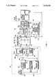
- FIG. 1 is a block diagram of the transformer isolated drive circuit according to the present invention.
- FIG. 2 is a block diagram of one embodiment of the transformer isolated drive circuit of the present invention implemented as first and second semiconductor devices coupled by a transformer;
- FIG. 3 is a timing diagram illustrating the voltage levels and timing signals of the transformer isolated drive circuit of the present invention.
- the transformer isolated drive circuit is shown in block diagram form in FIG. 1 wherein a voltage enable/control circuit 10 receives a low voltage load switch control signal on input lead 12.
- the load switch control signal is received from an external, low voltage circuit typically operating in the range of 0-5 volts.
- a retriggerable timer 14 provides a timed output signal on lead 16 having a preselected time period in response to at least one of the trigger signals on input leads 12 and 42.
- One of the trigger signals includes load switch control input signal on lead 12 which unconditionally retriggers retriggerable timer 14 regardless of the state of the timer's output signal on either the rising or falling edge of the signal.
- voltage enable and control circuit 10 provides a voltage control signal on lead 18 to first and second voltage sources 20 and 22 respectively.
- the first and second voltage sources 20,22 provide first and second voltage signals 24,26 respectively, at one of a plurality of voltage levels which provides a voltage signal at alternating positive and negative voltage potentials with reference to the first and second inputs "A" and "B" of transformer 30.
- the first and second voltage sources provide first and second voltage signals 24,26 at one of a high voltage level, a medium voltage level, and a low voltage level.
- First and second voltage sources 20,22 also include first and second current sense means 32,34.
- the current sense means provide first and second zero current indicator signals over leads 36,38 upon the detection of zero current flow in the primary winding of the transformer.
- trigger generator 40 which is responsive to the timed output signal on lead 16 from the retriggerable timer, the voltage control signal on lead 18, and the first and second zero current detection signals on leads 36,38, for providing a second retriggerable timer trigger signal on lead 42 upon the condition of zero current detected in the primary winding of the transformer as indicated by zero current indicator signals on leads 36,38 and upon the expiration of times output signal on lead 16 from retriggerable timer 14.
- the second retriggerable timer trigger signal on lead 42 is provided only after the preselected time period of timed output signal on lead 16 and then, only in conjunction with the detection of zero current flow in the primary winding of the transformer, assuring that any voltage applied to the primary winding of the transformer during the time period of the timed output signal on lead 16 has completely decayed or dropped to zero, and preventing transformer saturation.
- Transformer 30 also includes a secondary winding or side 44 in which is induced a voltage which is of the same polarity as the voltage applied to primary winding 28.
- the magnitude or level of the voltage induced in the transformer's secondary winding is dependent upon the turns ratio of the transformer.
- First and second outputs "A" and "B", 46,48 from the secondary winding 44 couple the induced voltage from the secondary winding of the transformer to at least voltage level sense means 50 and switch control means 51.
- the voltage level sense means detects the magnitude and polarity of the voltage induced across the secondary winding outputs 46,48, and enables switch control circuit 51 which in turn enables high voltage load switch 52, for providing power to load 54 in response to a first, sensed voltage level, and disables load switch 52 in response to a second, sensed voltage level and polarity, thus disabling power to load 54.
- the present invention also includes a power supply generator circuit 56, coupled to the first and second outputs 46,48 of the secondary winding 44 of the transformer, for providing a power signal on lead 58 to at least the voltage level sense circuitry 50 and the switch control circuit 51.
- a power supply generator circuit 56 coupled to the first and second outputs 46,48 of the secondary winding 44 of the transformer, for providing a power signal on lead 58 to at least the voltage level sense circuitry 50 and the switch control circuit 51.
- the voltage induced in the secondary winding 44 of the transformer provides both switch control and power for at least a portion of the sense circuit 74.
- drive circuit condition monitor circuit 60 comprising an under voltage monitor 62 coupled to power supply generator 56; a manual enable/disable monitor 64 coupled to an external enable/disable signal 66; and an over current monitor 68 coupled to load 54.
- the output 70 from condition monitoring circuit 60 is coupled to the switch control circuitry 51 and operates to appropriately enable and disable the high voltage load switch 52 in response to at least one of the plurality of monitored condition signals.
- the transformer isolated drive circuit according to the present invention is implemented on first and second semiconductor devices 72,74 respectively.
- the input stage of the drive circuit of the present invention is implemented on the first semiconductor device 72 which includes voltage enable/control circuit 10, retriggerable timer 14, retriggerable timer trigger generator 40, and first and second voltage sources 20,22.
- the input stage circuitry located on first semiconductor device 72 is responsive to load a switch control signal on input lead 12 and coupled to primary winding 28 of transformer 30 by means of first and second voltage output signals 24,26.
- the output or sense portion of the drive circuit of the present invention may be implemented on a second semiconductor device 74 including power supply generator 56, voltage level sense control circuit 50, switch control circuit 51, and condition monitor 60.
- FIG. 2 A preferred embodiment of the transformer isolated drive circuit of the present invention is shown in the block diagram of FIG. 2 which corresponds, although with greater detail, to FIG. 1.
- the circuit is implemented on first and second semiconductor devices 72,74 wherein the first semiconductor circuit 72 implements the input or receiver stage of the circuit and which generates a voltage signal of appropriate voltage and polarity which is coupled through transformer 30 to second semiconductor device 74 which senses the received signal and appropriately enables and disables load switch 52.
- the first semiconductor device 72 includes voltage enable/control circuit 10, retriggerable timer 14, trigger generator 40, and first and second voltage sources 20,22. Also included is bias voltage generator 76 which includes an under voltage lockout circuit which inhibits the output of the voltage sources 20,22 when the input supply voltage is below 9 volts. When adequate supply voltage is present, bias generator 76 supplies appropriate internal voltages and currents which allows voltage sources 20,22 to be enabled, thus assuring correct operation during circuit power-up and power-down.
- the overall time period which controls the operation of the first semiconductor device 72 is a function of both the pulse width generated by retriggerable timer 14 as well as the transformer core reset time.
- the pulse width of retriggerable timer 14 is set by timing resistor R T and timing capacitor C T at typically 600 nano seconds.
- the second semiconductor device 74 as previously shown in FIG. 1 includes voltage level and sense circuit 50, load switch control circuit 51, power supply generator circuit 56 and condition monitor circuit 60 including an under voltage monitor 62, manual control monitor 64 and over current monitor circuit 68.
- timing capacitor C T When the retriggerable timer 14 is triggered by the detection of zero current flow in the primary winding of the transformer at time period t 1 , timing capacitor C T is discharged. The "full" voltage of V high -V low , 80, is applied across the primary winding of the transformer causing a generally linear increase in the magnetizing current 78. At time t 2 , the voltage across timing capacitor C T reaches a 2.5 volt threshold ending the timer's timed output signal. Output A, 24, is switched to V medium which is generally equal to 1/2 (V high -V low ) and voltage on output B, 26, is switched to V high . The voltage applied to primary winding 28 of transformer 30 is thus reduced in half and its polarity inverted, 80, thus causing the magnetizing current 78 to fall at approximately one-half the rate at which it increased.
- current sense comparator 32 of voltage source 20 senses that the transformer's primary winding magnetizing current has reached zero and retriggers the retriggerable timer thus initiating another cycle. Operation of the circuit continues alternately recharging timing capacitor C T , sensing zero magnetizing current, and retriggering the circuit as shown at time periods t 4 , t 5 and t 6 .
- the rese in magnetizing current 78 in the primary winding of transformer 30 induces a current 82, in secondary winding 44 of the transformer which is of corresponding polarity as the magnetizing current induced in the primary winding and of a magnitude dependent upon the transformer's turn ratio.
- the current 82, induced in the secondary winding 44 of transformer 30 is sensed by voltage level sense comparator 50 which is a comparator with a hysteresis of 2Vcc.
- voltage level sense circuit 50 which disables switch control circuit 51 thus maintaining a low voltage 84 on the gate 53 of load switch 52.
- the load switch control signal on input lead 12 transitions from low to high, indicting that the user of the circuit wishes to enable the load switch. Accordingly, the rising edge of the load switch control signal triggers the retriggerable timer 14 initiating a new cycle period and terminating the existing cycle.
- the "high" on load switch control signal input lead 12 is decoded by voltage enable/control circuit 10 and the polarity of the voltage on the two voltage sources 20,22 are reversed thus placing a "high" voltage on the B output 26 and a low voltage on A output 24.
- the difference in applied voltage generate a reversed polarity voltage and current 78 in the primary winding of transformer 30, thus inducing a voltage and current 82 of corresponding voltage level and polarity in the secondary winding 44 of transformer 30.
- the voltage induced across the transformer's secondary winding 44 is sensed by voltage level sense comparator 50. Since the voltage transitions to -Vcc, voltage level sense comparator 50 detects the change in voltage and provides a signal enabling load switch control circuit 51 which in turn applies the appropriate e.g. positive going signal 84, to the gate 53 of load switch FET 52.
- load switch control signal 84 remains in an active state through time period t 14 since the voltage induced by the secondary winding current 82 does not exceed the hysteresis (2 Vcc) of voltage level sense comparator 50.
- timing capacitor C T reaches the 2.5 volt threshold which ends the time period of retriggerable timer 14, thus allowing the magnetizing current 78 to decay until at time period t 9 , current sense comparator 34 of the second voltage source 22 detects a zero current in the primary winding 28 of transformer 30 causing trigger generator 40 to generate trigger signal 42 and thus initiating a new cycle period.
- the circuit operation during periods t 7 through t 13 are identical to the operation of the circuit described in relation to time periods t 1 through t 6 with the exception that the voltage on outputs A and B, 24-26, are reversed.
- Voltage enable/control circuit 10 under command from the load switch control signal, directs the first and second voltage sources 20,22 to reverse polarity thus applying a high voltage of a positive polarity on the A output of 24 with respect to the B output 26. This applied voltage causes a corresponding change in magnetizing current 78 and secondary current 82 thus inducing a 2 Vcc voltage change which is sensed by voltage sense comparator 50 thus providing a disable signal 84 on the gate 53 of load switch FET 52. Operation of the circuit then continues as described in relation to time periods t 1 through t 6 .
Abstract
Description
Claims (13)
Priority Applications (1)
| Application Number | Priority Date | Filing Date | Title |
|---|---|---|---|
| US07/697,895 US5206540A (en) | 1991-05-09 | 1991-05-09 | Transformer isolated drive circuit |
Applications Claiming Priority (1)
| Application Number | Priority Date | Filing Date | Title |
|---|---|---|---|
| US07/697,895 US5206540A (en) | 1991-05-09 | 1991-05-09 | Transformer isolated drive circuit |
Publications (1)
| Publication Number | Publication Date |
|---|---|
| US5206540A true US5206540A (en) | 1993-04-27 |
Family
ID=24803029
Family Applications (1)
| Application Number | Title | Priority Date | Filing Date |
|---|---|---|---|
| US07/697,895 Expired - Lifetime US5206540A (en) | 1991-05-09 | 1991-05-09 | Transformer isolated drive circuit |
Country Status (1)
| Country | Link |
|---|---|
| US (1) | US5206540A (en) |
Cited By (56)
| Publication number | Priority date | Publication date | Assignee | Title |
|---|---|---|---|---|
| US5274274A (en) * | 1992-03-23 | 1993-12-28 | Power Integrations, Inc. | Dual threshold differential discriminator |
| US5329193A (en) * | 1992-11-12 | 1994-07-12 | Lu Chao Cheng | Computer controller |
| EP0652639A2 (en) * | 1993-11-08 | 1995-05-10 | GRÜNDL UND HOFFMANN GmbH GESELLSCHAFT FÜR ELEKTROTECHNISCHE ENTWICKLUNGEN | Driver circuit |
| US5841621A (en) * | 1994-03-17 | 1998-11-24 | Fmc Corporation | Sensorless measurement of electromagnetic actuator displacement device |
| US5900683A (en) * | 1997-12-23 | 1999-05-04 | Ford Global Technologies, Inc. | Isolated gate driver for power switching device and method for carrying out same |
| US6148804A (en) * | 1999-11-22 | 2000-11-21 | Daimlerchrysler Corporation | Duty cycling feature for the proportional purge solenoid to improve low flow resolution |
| US6154477A (en) * | 1997-05-13 | 2000-11-28 | Berkeley Research Associates, Inc. | On-board laser-triggered multi-layer semiconductor power switch |
| US6208121B1 (en) | 1998-01-20 | 2001-03-27 | Iap Research, Inc. | Switching power supply with AC waveform capability |
| US6246598B1 (en) | 2000-08-02 | 2001-06-12 | Polarity, Inc. | High-voltage modulator system |
| WO2005096499A1 (en) * | 2004-04-01 | 2005-10-13 | Danfoss A/S | An electronic switch |
| US20070046501A1 (en) * | 2005-08-30 | 2007-03-01 | Chun-Hsiao Wang | Electromagnetic coupling galvanic isolated digital output circuit with output feedback |
| US20080224636A1 (en) * | 2007-03-12 | 2008-09-18 | Melanson John L | Power control system for current regulated light sources |
| US20080224631A1 (en) * | 2007-03-12 | 2008-09-18 | Melanson John L | Color variations in a dimmable lighting device with stable color temperature light sources |
| US20080240789A1 (en) * | 2007-03-28 | 2008-10-02 | Fuji Xerox Co., Ltd. | Rotator for powder conveyance and toner cartridge |
| US20080272746A1 (en) * | 2007-05-02 | 2008-11-06 | Cirrus Logic, Inc. | Power factor correction controller with switch node feedback |
| US20090147544A1 (en) * | 2007-12-11 | 2009-06-11 | Melanson John L | Modulated transformer-coupled gate control signaling method and apparatus |
| US20090147545A1 (en) * | 2007-12-11 | 2009-06-11 | Melanson John L | History-independent noise-immune modulated transformer-coupled gate control signaling method and apparatus |
| US20090191837A1 (en) * | 2008-01-30 | 2009-07-30 | Kartik Nanda | Delta Sigma Modulator with Unavailable Output Values |
| US20090190384A1 (en) * | 2008-01-30 | 2009-07-30 | Cirrus Logic, Inc. | Powering a power supply integrated circuit with sense current |
| US20090190379A1 (en) * | 2008-01-30 | 2009-07-30 | John L Melanson | Switching regulator with boosted auxiliary winding supply |
| US20090189579A1 (en) * | 2008-01-30 | 2009-07-30 | Melanson John L | Switch state controller with a sense current generated operating voltage |
| US20090212759A1 (en) * | 2008-02-26 | 2009-08-27 | Melanson John L | Transformer-isolated analog-to-digital converter (adc) feedback apparatus and method |
| US20090322300A1 (en) * | 2008-06-25 | 2009-12-31 | Melanson John L | Hysteretic buck converter having dynamic thresholds |
| US20100020569A1 (en) * | 2008-07-25 | 2010-01-28 | Melanson John L | Resonant switching power converter with adaptive dead time control |
| US7660137B1 (en) | 2006-07-26 | 2010-02-09 | Polarity, Inc. | High-voltage modulator system |
| US20100060202A1 (en) * | 2007-03-12 | 2010-03-11 | Melanson John L | Lighting System with Lighting Dimmer Output Mapping |
| US20100079125A1 (en) * | 2008-07-25 | 2010-04-01 | Melanson John L | Current sensing in a switching power converter |
| US20100079124A1 (en) * | 2008-09-30 | 2010-04-01 | John Laurence Melanson | Adjustable Constant Current Source with Continuous Conduction Mode ("CCM") and Discontinuous Conduction Mode ("DCM") Operation |
| US20100148677A1 (en) * | 2008-12-12 | 2010-06-17 | Melanson John L | Time division light output sensing and brightness adjustment for different spectra of light emitting diodes |
| US20100164406A1 (en) * | 2008-07-25 | 2010-07-01 | Kost Michael A | Switching power converter control with triac-based leading edge dimmer compatibility |
| US20100164631A1 (en) * | 2008-12-31 | 2010-07-01 | Cirrus Logic, Inc. | Electronic system having common mode voltage range enhancement |
| US7759881B1 (en) | 2008-03-31 | 2010-07-20 | Cirrus Logic, Inc. | LED lighting system with a multiple mode current control dimming strategy |
| US20100277072A1 (en) * | 2009-04-30 | 2010-11-04 | Draper William A | Calibration Of Lamps |
| US20100328976A1 (en) * | 2009-06-30 | 2010-12-30 | Melanson John L | Cascode configured switching using at least one low breakdown voltage internal, integrated circuit switch to control at least one high breakdown voltage external switch |
| US20100327838A1 (en) * | 2009-06-30 | 2010-12-30 | Melanson John L | Switching power converter with current sensing transformer auxiliary power supply |
| US20110074302A1 (en) * | 2009-09-30 | 2011-03-31 | Draper William A | Phase Control Dimming Compatible Lighting Systems |
| US20110110000A1 (en) * | 2009-11-09 | 2011-05-12 | Etter Brett E | Power System Having Voltage-Based Monitoring for Over Current Protection |
| US7965522B1 (en) | 2008-09-26 | 2011-06-21 | Arkansas Power Electronics International, Inc. | Low-loss noise-resistant high-temperature gate driver circuits |
| US8018171B1 (en) | 2007-03-12 | 2011-09-13 | Cirrus Logic, Inc. | Multi-function duty cycle modifier |
| US8076920B1 (en) | 2007-03-12 | 2011-12-13 | Cirrus Logic, Inc. | Switching power converter and control system |
| US8102127B2 (en) | 2007-06-24 | 2012-01-24 | Cirrus Logic, Inc. | Hybrid gas discharge lamp-LED lighting system |
| US8212493B2 (en) | 2009-06-30 | 2012-07-03 | Cirrus Logic, Inc. | Low energy transfer mode for auxiliary power supply operation in a cascaded switching power converter |
| US8222872B1 (en) | 2008-09-30 | 2012-07-17 | Cirrus Logic, Inc. | Switching power converter with selectable mode auxiliary power supply |
| US8288954B2 (en) | 2008-12-07 | 2012-10-16 | Cirrus Logic, Inc. | Primary-side based control of secondary-side current for a transformer |
| US8362707B2 (en) | 2008-12-12 | 2013-01-29 | Cirrus Logic, Inc. | Light emitting diode based lighting system with time division ambient light feedback response |
| WO2013016550A2 (en) * | 2011-07-27 | 2013-01-31 | The Watt Stopper, Inc. | Method and apparatus for isolating high voltage power control elements |
| US8487546B2 (en) | 2008-08-29 | 2013-07-16 | Cirrus Logic, Inc. | LED lighting system with accurate current control |
| DE102013205706A1 (en) * | 2013-03-28 | 2014-10-02 | Fraunhofer-Gesellschaft zur Förderung der angewandten Forschung e.V. | POWER ELECTRONIC SWITCHING AND SYSTEM WITH THE SAME |
| US8963535B1 (en) | 2009-06-30 | 2015-02-24 | Cirrus Logic, Inc. | Switch controlled current sensing using a hall effect sensor |
| CN102902297B (en) * | 2011-07-27 | 2016-11-30 | 瓦特制动器有限公司 | For isolating the method and apparatus that high-voltage power controls element |
| WO2018095619A1 (en) * | 2016-11-24 | 2018-05-31 | Siemens Aktiengesellschaft | Actuation assembly for voltage-controlled switching elements |
| US10051701B2 (en) | 2014-07-16 | 2018-08-14 | Philips Lighting Holding B.V. | Systems and methods for maintaining dimmer behavior in a low-power lamp assembly |
| CN109270149A (en) * | 2017-07-17 | 2019-01-25 | 梅特勒-托莱多有限公司 | For monitoring and/or determining the improved method and device of the situation of measuring probe |
| TWI657653B (en) * | 2018-06-12 | 2019-04-21 | 大陸商昂寶電子(上海)有限公司 | Power conversion system |
| US10812069B1 (en) | 2019-08-06 | 2020-10-20 | Baker Hughes, A Ge Company, Llc | Isolated switch driving circuit |
| EP3624318B1 (en) * | 2018-09-12 | 2021-11-17 | ABB Schweiz AG | Transmitting energy and a data signal via a transformer |
Citations (7)
| Publication number | Priority date | Publication date | Assignee | Title |
|---|---|---|---|---|
| US3675051A (en) * | 1970-06-24 | 1972-07-04 | Gen Electric | Hand proximity alarm control circuit |
| US4052623A (en) * | 1976-08-10 | 1977-10-04 | General Electric Company | Isolated semiconductor gate control circuit |
| US4438356A (en) * | 1982-03-24 | 1984-03-20 | International Rectifier Corporation | Solid state relay circuit employing MOSFET power switching devices |
| US4461966A (en) * | 1980-12-04 | 1984-07-24 | Siemens Aktiengesellschaft | Circuit for controlling at least one power-FET |
| US4634903A (en) * | 1984-02-20 | 1987-01-06 | Honeywell Information Systems Italia | Power FET driving circuit |
| US4792746A (en) * | 1987-05-11 | 1988-12-20 | Astec Components, Ltd. | Non-dissipative series voltage switching regulator having improved switching speed |
| US4876624A (en) * | 1988-07-13 | 1989-10-24 | Westinghouse Electric Corp. | Apparatus for detecting unsymmetrical bipolar waveforms |
-
1991
- 1991-05-09 US US07/697,895 patent/US5206540A/en not_active Expired - Lifetime
Patent Citations (7)
| Publication number | Priority date | Publication date | Assignee | Title |
|---|---|---|---|---|
| US3675051A (en) * | 1970-06-24 | 1972-07-04 | Gen Electric | Hand proximity alarm control circuit |
| US4052623A (en) * | 1976-08-10 | 1977-10-04 | General Electric Company | Isolated semiconductor gate control circuit |
| US4461966A (en) * | 1980-12-04 | 1984-07-24 | Siemens Aktiengesellschaft | Circuit for controlling at least one power-FET |
| US4438356A (en) * | 1982-03-24 | 1984-03-20 | International Rectifier Corporation | Solid state relay circuit employing MOSFET power switching devices |
| US4634903A (en) * | 1984-02-20 | 1987-01-06 | Honeywell Information Systems Italia | Power FET driving circuit |
| US4792746A (en) * | 1987-05-11 | 1988-12-20 | Astec Components, Ltd. | Non-dissipative series voltage switching regulator having improved switching speed |
| US4876624A (en) * | 1988-07-13 | 1989-10-24 | Westinghouse Electric Corp. | Apparatus for detecting unsymmetrical bipolar waveforms |
Non-Patent Citations (4)
| Title |
|---|
| "Gate Drive Requirements," Section 1-Chapter 6, Motorola Power MOSFET Transistor Databook, 1988, pp. 1-6-2-1-6-22. |
| Gate Drive Requirements, Section 1 Chapter 6, Motorola Power MOSFET Transistor Databook, 1988, pp. 1 6 2 1 6 22. * |
| Wood, P., "Transformer-Isolated HEXFET Driver Provides very large duty cycle ratios," International Rectifier, Chapter 15, Application Note 950A, pp. A-141-A-143. |
| Wood, P., Transformer Isolated HEXFET Driver Provides very large duty cycle ratios, International Rectifier, Chapter 15, Application Note 950A, pp. A 141 A 143. * |
Cited By (105)
| Publication number | Priority date | Publication date | Assignee | Title |
|---|---|---|---|---|
| US5274274A (en) * | 1992-03-23 | 1993-12-28 | Power Integrations, Inc. | Dual threshold differential discriminator |
| US5329193A (en) * | 1992-11-12 | 1994-07-12 | Lu Chao Cheng | Computer controller |
| EP0652639A2 (en) * | 1993-11-08 | 1995-05-10 | GRÜNDL UND HOFFMANN GmbH GESELLSCHAFT FÜR ELEKTROTECHNISCHE ENTWICKLUNGEN | Driver circuit |
| EP0652639A3 (en) * | 1993-11-08 | 1996-05-15 | Gruendl & Hoffmann | Driver circuit. |
| US5841621A (en) * | 1994-03-17 | 1998-11-24 | Fmc Corporation | Sensorless measurement of electromagnetic actuator displacement device |
| US6154477A (en) * | 1997-05-13 | 2000-11-28 | Berkeley Research Associates, Inc. | On-board laser-triggered multi-layer semiconductor power switch |
| US5900683A (en) * | 1997-12-23 | 1999-05-04 | Ford Global Technologies, Inc. | Isolated gate driver for power switching device and method for carrying out same |
| US6208121B1 (en) | 1998-01-20 | 2001-03-27 | Iap Research, Inc. | Switching power supply with AC waveform capability |
| US6465995B2 (en) | 1998-01-20 | 2002-10-15 | Iap Research, Inc. | Switching power supply with AC waveform capability |
| US6148804A (en) * | 1999-11-22 | 2000-11-21 | Daimlerchrysler Corporation | Duty cycling feature for the proportional purge solenoid to improve low flow resolution |
| US6246598B1 (en) | 2000-08-02 | 2001-06-12 | Polarity, Inc. | High-voltage modulator system |
| WO2005096499A1 (en) * | 2004-04-01 | 2005-10-13 | Danfoss A/S | An electronic switch |
| US20070046501A1 (en) * | 2005-08-30 | 2007-03-01 | Chun-Hsiao Wang | Electromagnetic coupling galvanic isolated digital output circuit with output feedback |
| US7443276B2 (en) * | 2005-08-30 | 2008-10-28 | Netio Networking Technology | Electromagnetic coupling galvanic isolated digital output circuit with output feedback |
| US8208275B2 (en) | 2006-07-26 | 2012-06-26 | Polarity, Inc. | High-voltage modulator system |
| US7660137B1 (en) | 2006-07-26 | 2010-02-09 | Polarity, Inc. | High-voltage modulator system |
| US7852017B1 (en) | 2007-03-12 | 2010-12-14 | Cirrus Logic, Inc. | Ballast for light emitting diode light sources |
| US7804256B2 (en) | 2007-03-12 | 2010-09-28 | Cirrus Logic, Inc. | Power control system for current regulated light sources |
| US20080224636A1 (en) * | 2007-03-12 | 2008-09-18 | Melanson John L | Power control system for current regulated light sources |
| US8018171B1 (en) | 2007-03-12 | 2011-09-13 | Cirrus Logic, Inc. | Multi-function duty cycle modifier |
| US20100060202A1 (en) * | 2007-03-12 | 2010-03-11 | Melanson John L | Lighting System with Lighting Dimmer Output Mapping |
| US20080224631A1 (en) * | 2007-03-12 | 2008-09-18 | Melanson John L | Color variations in a dimmable lighting device with stable color temperature light sources |
| US8076920B1 (en) | 2007-03-12 | 2011-12-13 | Cirrus Logic, Inc. | Switching power converter and control system |
| US8174204B2 (en) | 2007-03-12 | 2012-05-08 | Cirrus Logic, Inc. | Lighting system with power factor correction control data determined from a phase modulated signal |
| US8536794B2 (en) | 2007-03-12 | 2013-09-17 | Cirrus Logic, Inc. | Lighting system with lighting dimmer output mapping |
| US20080224629A1 (en) * | 2007-03-12 | 2008-09-18 | Melanson John L | Lighting system with power factor correction control data determined from a phase modulated signal |
| US20080240789A1 (en) * | 2007-03-28 | 2008-10-02 | Fuji Xerox Co., Ltd. | Rotator for powder conveyance and toner cartridge |
| US20080272758A1 (en) * | 2007-05-02 | 2008-11-06 | Melanson John L | Switching Power Converter with Switch Control Pulse Width Variability at Low Power Demand Levels |
| US7888922B2 (en) | 2007-05-02 | 2011-02-15 | Cirrus Logic, Inc. | Power factor correction controller with switch node feedback |
| US8125805B1 (en) | 2007-05-02 | 2012-02-28 | Cirrus Logic Inc. | Switch-mode converter operating in a hybrid discontinuous conduction mode (DCM)/continuous conduction mode (CCM) that uses double or more pulses in a switching period |
| US8120341B2 (en) | 2007-05-02 | 2012-02-21 | Cirrus Logic, Inc. | Switching power converter with switch control pulse width variability at low power demand levels |
| US20080272746A1 (en) * | 2007-05-02 | 2008-11-06 | Cirrus Logic, Inc. | Power factor correction controller with switch node feedback |
| US7821237B2 (en) | 2007-05-02 | 2010-10-26 | Cirrus Logic, Inc. | Power factor correction (PFC) controller and method using a finite state machine to adjust the duty cycle of a PWM control signal |
| US8040703B2 (en) | 2007-05-02 | 2011-10-18 | Cirrus Logic, Inc. | Power factor correction controller with feedback reduction |
| US20080272747A1 (en) * | 2007-05-02 | 2008-11-06 | Cirrus Logic, Inc. | Programmable power control system |
| US7863828B2 (en) | 2007-05-02 | 2011-01-04 | Cirrus Logic, Inc. | Power supply DC voltage offset detector |
| US20080273356A1 (en) * | 2007-05-02 | 2008-11-06 | Melanson John L | Switching Power Converter with Efficient Switching Control Signal Period Generation |
| US20080272756A1 (en) * | 2007-05-02 | 2008-11-06 | Melanson John L | Power factor correction controller with digital fir filter output voltage sampling |
| US7969125B2 (en) | 2007-05-02 | 2011-06-28 | Cirrus Logic, Inc. | Programmable power control system |
| US7894216B2 (en) | 2007-05-02 | 2011-02-22 | Cirrus Logic, Inc. | Switching power converter with efficient switching control signal period generation |
| US8102127B2 (en) | 2007-06-24 | 2012-01-24 | Cirrus Logic, Inc. | Hybrid gas discharge lamp-LED lighting system |
| US20090147545A1 (en) * | 2007-12-11 | 2009-06-11 | Melanson John L | History-independent noise-immune modulated transformer-coupled gate control signaling method and apparatus |
| US7804697B2 (en) | 2007-12-11 | 2010-09-28 | Cirrus Logic, Inc. | History-independent noise-immune modulated transformer-coupled gate control signaling method and apparatus |
| US7656687B2 (en) | 2007-12-11 | 2010-02-02 | Cirrus Logic, Inc. | Modulated transformer-coupled gate control signaling method and apparatus |
| US20090147544A1 (en) * | 2007-12-11 | 2009-06-11 | Melanson John L | Modulated transformer-coupled gate control signaling method and apparatus |
| US20090190384A1 (en) * | 2008-01-30 | 2009-07-30 | Cirrus Logic, Inc. | Powering a power supply integrated circuit with sense current |
| US8008898B2 (en) | 2008-01-30 | 2011-08-30 | Cirrus Logic, Inc. | Switching regulator with boosted auxiliary winding supply |
| US8576589B2 (en) | 2008-01-30 | 2013-11-05 | Cirrus Logic, Inc. | Switch state controller with a sense current generated operating voltage |
| US7755525B2 (en) | 2008-01-30 | 2010-07-13 | Cirrus Logic, Inc. | Delta sigma modulator with unavailable output values |
| US20090191837A1 (en) * | 2008-01-30 | 2009-07-30 | Kartik Nanda | Delta Sigma Modulator with Unavailable Output Values |
| US20090190379A1 (en) * | 2008-01-30 | 2009-07-30 | John L Melanson | Switching regulator with boosted auxiliary winding supply |
| US20090189579A1 (en) * | 2008-01-30 | 2009-07-30 | Melanson John L | Switch state controller with a sense current generated operating voltage |
| US8022683B2 (en) | 2008-01-30 | 2011-09-20 | Cirrus Logic, Inc. | Powering a power supply integrated circuit with sense current |
| US20090212759A1 (en) * | 2008-02-26 | 2009-08-27 | Melanson John L | Transformer-isolated analog-to-digital converter (adc) feedback apparatus and method |
| US7796076B2 (en) | 2008-02-26 | 2010-09-14 | Cirrus Logic, Inc. | Transformer-isolated analog-to-digital converter (ADC) feedback apparatus and method |
| US7759881B1 (en) | 2008-03-31 | 2010-07-20 | Cirrus Logic, Inc. | LED lighting system with a multiple mode current control dimming strategy |
| US8008902B2 (en) | 2008-06-25 | 2011-08-30 | Cirrus Logic, Inc. | Hysteretic buck converter having dynamic thresholds |
| US20090322300A1 (en) * | 2008-06-25 | 2009-12-31 | Melanson John L | Hysteretic buck converter having dynamic thresholds |
| US8344707B2 (en) | 2008-07-25 | 2013-01-01 | Cirrus Logic, Inc. | Current sensing in a switching power converter |
| US8212491B2 (en) | 2008-07-25 | 2012-07-03 | Cirrus Logic, Inc. | Switching power converter control with triac-based leading edge dimmer compatibility |
| US8553430B2 (en) | 2008-07-25 | 2013-10-08 | Cirrus Logic, Inc. | Resonant switching power converter with adaptive dead time control |
| US8014176B2 (en) | 2008-07-25 | 2011-09-06 | Cirrus Logic, Inc. | Resonant switching power converter with burst mode transition shaping |
| US20100079125A1 (en) * | 2008-07-25 | 2010-04-01 | Melanson John L | Current sensing in a switching power converter |
| US20100020570A1 (en) * | 2008-07-25 | 2010-01-28 | Melanson John L | Resonant switching power converter with burst mode transition shaping |
| US20100020573A1 (en) * | 2008-07-25 | 2010-01-28 | Melanson John L | Audible noise suppression in a resonant switching power converter |
| US20100020569A1 (en) * | 2008-07-25 | 2010-01-28 | Melanson John L | Resonant switching power converter with adaptive dead time control |
| US8279628B2 (en) | 2008-07-25 | 2012-10-02 | Cirrus Logic, Inc. | Audible noise suppression in a resonant switching power converter |
| US20100164406A1 (en) * | 2008-07-25 | 2010-07-01 | Kost Michael A | Switching power converter control with triac-based leading edge dimmer compatibility |
| US8487546B2 (en) | 2008-08-29 | 2013-07-16 | Cirrus Logic, Inc. | LED lighting system with accurate current control |
| US7965522B1 (en) | 2008-09-26 | 2011-06-21 | Arkansas Power Electronics International, Inc. | Low-loss noise-resistant high-temperature gate driver circuits |
| US20100079124A1 (en) * | 2008-09-30 | 2010-04-01 | John Laurence Melanson | Adjustable Constant Current Source with Continuous Conduction Mode ("CCM") and Discontinuous Conduction Mode ("DCM") Operation |
| US8222872B1 (en) | 2008-09-30 | 2012-07-17 | Cirrus Logic, Inc. | Switching power converter with selectable mode auxiliary power supply |
| US8179110B2 (en) | 2008-09-30 | 2012-05-15 | Cirrus Logic Inc. | Adjustable constant current source with continuous conduction mode (“CCM”) and discontinuous conduction mode (“DCM”) operation |
| US8288954B2 (en) | 2008-12-07 | 2012-10-16 | Cirrus Logic, Inc. | Primary-side based control of secondary-side current for a transformer |
| US20100148677A1 (en) * | 2008-12-12 | 2010-06-17 | Melanson John L | Time division light output sensing and brightness adjustment for different spectra of light emitting diodes |
| US8362707B2 (en) | 2008-12-12 | 2013-01-29 | Cirrus Logic, Inc. | Light emitting diode based lighting system with time division ambient light feedback response |
| US8299722B2 (en) | 2008-12-12 | 2012-10-30 | Cirrus Logic, Inc. | Time division light output sensing and brightness adjustment for different spectra of light emitting diodes |
| US7994863B2 (en) | 2008-12-31 | 2011-08-09 | Cirrus Logic, Inc. | Electronic system having common mode voltage range enhancement |
| US20100164631A1 (en) * | 2008-12-31 | 2010-07-01 | Cirrus Logic, Inc. | Electronic system having common mode voltage range enhancement |
| US20100277072A1 (en) * | 2009-04-30 | 2010-11-04 | Draper William A | Calibration Of Lamps |
| US8482223B2 (en) | 2009-04-30 | 2013-07-09 | Cirrus Logic, Inc. | Calibration of lamps |
| US8248145B2 (en) | 2009-06-30 | 2012-08-21 | Cirrus Logic, Inc. | Cascode configured switching using at least one low breakdown voltage internal, integrated circuit switch to control at least one high breakdown voltage external switch |
| US20100327838A1 (en) * | 2009-06-30 | 2010-12-30 | Melanson John L | Switching power converter with current sensing transformer auxiliary power supply |
| US8963535B1 (en) | 2009-06-30 | 2015-02-24 | Cirrus Logic, Inc. | Switch controlled current sensing using a hall effect sensor |
| US8212493B2 (en) | 2009-06-30 | 2012-07-03 | Cirrus Logic, Inc. | Low energy transfer mode for auxiliary power supply operation in a cascaded switching power converter |
| US20100328976A1 (en) * | 2009-06-30 | 2010-12-30 | Melanson John L | Cascode configured switching using at least one low breakdown voltage internal, integrated circuit switch to control at least one high breakdown voltage external switch |
| US8198874B2 (en) | 2009-06-30 | 2012-06-12 | Cirrus Logic, Inc. | Switching power converter with current sensing transformer auxiliary power supply |
| US9155174B2 (en) | 2009-09-30 | 2015-10-06 | Cirrus Logic, Inc. | Phase control dimming compatible lighting systems |
| US20110074302A1 (en) * | 2009-09-30 | 2011-03-31 | Draper William A | Phase Control Dimming Compatible Lighting Systems |
| US20110110000A1 (en) * | 2009-11-09 | 2011-05-12 | Etter Brett E | Power System Having Voltage-Based Monitoring for Over Current Protection |
| US8654483B2 (en) | 2009-11-09 | 2014-02-18 | Cirrus Logic, Inc. | Power system having voltage-based monitoring for over current protection |
| US8638539B2 (en) | 2011-07-27 | 2014-01-28 | The Watt Stopper, Inc. | Method and apparatus for isolating high voltage power control elements |
| CN106444955B (en) * | 2011-07-27 | 2018-03-23 | 瓦特制动器有限公司 | Method and apparatus for isolating high-voltage power control element |
| WO2013016550A3 (en) * | 2011-07-27 | 2013-06-13 | The Watt Stopper, Inc. | Method and apparatus for isolating high voltage power control elements |
| WO2013016550A2 (en) * | 2011-07-27 | 2013-01-31 | The Watt Stopper, Inc. | Method and apparatus for isolating high voltage power control elements |
| CN102902297B (en) * | 2011-07-27 | 2016-11-30 | 瓦特制动器有限公司 | For isolating the method and apparatus that high-voltage power controls element |
| CN106444955A (en) * | 2011-07-27 | 2017-02-22 | 瓦特制动器有限公司 | Method and apparatus for isolating high voltage power control elements |
| DE102013205706A1 (en) * | 2013-03-28 | 2014-10-02 | Fraunhofer-Gesellschaft zur Förderung der angewandten Forschung e.V. | POWER ELECTRONIC SWITCHING AND SYSTEM WITH THE SAME |
| US9929566B2 (en) | 2013-03-28 | 2018-03-27 | Fraunhofer-Gesellschaft Zur Foerderung Der Angewandten Forschung E.V. | Power electronic circuit and system comprising the same |
| US10051701B2 (en) | 2014-07-16 | 2018-08-14 | Philips Lighting Holding B.V. | Systems and methods for maintaining dimmer behavior in a low-power lamp assembly |
| WO2018095619A1 (en) * | 2016-11-24 | 2018-05-31 | Siemens Aktiengesellschaft | Actuation assembly for voltage-controlled switching elements |
| CN109270149A (en) * | 2017-07-17 | 2019-01-25 | 梅特勒-托莱多有限公司 | For monitoring and/or determining the improved method and device of the situation of measuring probe |
| TWI657653B (en) * | 2018-06-12 | 2019-04-21 | 大陸商昂寶電子(上海)有限公司 | Power conversion system |
| EP3624318B1 (en) * | 2018-09-12 | 2021-11-17 | ABB Schweiz AG | Transmitting energy and a data signal via a transformer |
| US10812069B1 (en) | 2019-08-06 | 2020-10-20 | Baker Hughes, A Ge Company, Llc | Isolated switch driving circuit |
Similar Documents
| Publication | Publication Date | Title |
|---|---|---|
| US5206540A (en) | Transformer isolated drive circuit | |
| US5298797A (en) | Gate charge recovery circuit for gate-driven semiconductor devices | |
| US4748532A (en) | Transformer coupled power switching circuit | |
| US4156273A (en) | Protection of a switching regulator | |
| US5963438A (en) | Bi-directional magnetic isolator | |
| EP0938813B1 (en) | Quick-reset circuit for auxiliary power supply | |
| US6385060B1 (en) | Switching power supply with reduced energy transfer during a fault condition | |
| US7403366B2 (en) | Control circuit for an electromagnetic drive | |
| JPH0313827B2 (en) | ||
| WO1998021813A1 (en) | Auxiliary power supply control | |
| US20070273343A1 (en) | Supply Unit for a Driver Circuit and Method for Operating Same | |
| US7054171B1 (en) | Limiting the continuous mode of a power converter | |
| KR930004375Y1 (en) | Inverter protective circuit | |
| KR100310204B1 (en) | Circuit for removing residual magnetism of cathode ray tube according to degaussing coil | |
| JPH0583934A (en) | Power supply circuit | |
| JPH06106020B2 (en) | Switching regulator | |
| JP2752796B2 (en) | Switching power supply circuit | |
| KR100561721B1 (en) | Safety device of transformer for neon | |
| JPH04200276A (en) | Power supply device | |
| KR920004324Y1 (en) | Voltage regulator | |
| JPS5710820A (en) | Constant voltage power supply device | |
| JPH05300731A (en) | Overcurrent protection circuit of switching power supply | |
| JP2629585B2 (en) | Inrush current suppression circuit | |
| KR0147219B1 (en) | Low voltage protection circuit of power supply system | |
| JPH031909B2 (en) |
Legal Events
| Date | Code | Title | Description |
|---|---|---|---|
| AS | Assignment |
Owner name: UNITRODE CORPORATION A MARYLAND CORPORATION, MA Free format text: ASSIGNMENT OF ASSIGNORS INTEREST.;ASSIGNORS:DE SA E SILVA, CLAUDIO;PUTSCH, JEFFREY D.;HOLLAND, VARNUM S.;AND OTHERS;REEL/FRAME:005714/0320;SIGNING DATES FROM 19910325 TO 19910423 |
|
| AS | Assignment |
Owner name: UNITRODE CORPORATION A CORP. OF MD Free format text: CHANGE OF ADDRESS OF ASSIGNEE.;ASSIGNOR:UNITRODE CORPORATION, A MD CORP. 5 FORBES RD., LEXINGTON, MA 02173;REEL/FRAME:005919/0244 Effective date: 19911114 |
|
| STCF | Information on status: patent grant |
Free format text: PATENTED CASE |
|
| CC | Certificate of correction | ||
| FEPP | Fee payment procedure |
Free format text: PAYOR NUMBER ASSIGNED (ORIGINAL EVENT CODE: ASPN); ENTITY STATUS OF PATENT OWNER: LARGE ENTITY |
|
| FPAY | Fee payment |
Year of fee payment: 4 |
|
| FPAY | Fee payment |
Year of fee payment: 8 |
|
| FPAY | Fee payment |
Year of fee payment: 12 |