US5230068A - Cache memory system for dynamically altering single cache memory line as either branch target entry or pre-fetch instruction queue based upon instruction sequence - Google Patents
Cache memory system for dynamically altering single cache memory line as either branch target entry or pre-fetch instruction queue based upon instruction sequence Download PDFInfo
- Publication number
- US5230068A US5230068A US07/485,304 US48530490A US5230068A US 5230068 A US5230068 A US 5230068A US 48530490 A US48530490 A US 48530490A US 5230068 A US5230068 A US 5230068A
- Authority
- US
- United States
- Prior art keywords
- instruction
- branch
- cache memory
- queue
- branch target
- Prior art date
- Legal status (The legal status is an assumption and is not a legal conclusion. Google has not performed a legal analysis and makes no representation as to the accuracy of the status listed.)
- Expired - Lifetime
Links
Images


Classifications
-
- G—PHYSICS
- G06—COMPUTING; CALCULATING OR COUNTING
- G06F—ELECTRIC DIGITAL DATA PROCESSING
- G06F9/00—Arrangements for program control, e.g. control units
- G06F9/06—Arrangements for program control, e.g. control units using stored programs, i.e. using an internal store of processing equipment to receive or retain programs
- G06F9/30—Arrangements for executing machine instructions, e.g. instruction decode
- G06F9/38—Concurrent instruction execution, e.g. pipeline, look ahead
- G06F9/3802—Instruction prefetching
- G06F9/3804—Instruction prefetching for branches, e.g. hedging, branch folding
- G06F9/3806—Instruction prefetching for branches, e.g. hedging, branch folding using address prediction, e.g. return stack, branch history buffer
-
- G—PHYSICS
- G06—COMPUTING; CALCULATING OR COUNTING
- G06F—ELECTRIC DIGITAL DATA PROCESSING
- G06F9/00—Arrangements for program control, e.g. control units
- G06F9/06—Arrangements for program control, e.g. control units using stored programs, i.e. using an internal store of processing equipment to receive or retain programs
- G06F9/30—Arrangements for executing machine instructions, e.g. instruction decode
- G06F9/38—Concurrent instruction execution, e.g. pipeline, look ahead
- G06F9/3802—Instruction prefetching
- G06F9/3804—Instruction prefetching for branches, e.g. hedging, branch folding
-
- G—PHYSICS
- G06—COMPUTING; CALCULATING OR COUNTING
- G06F—ELECTRIC DIGITAL DATA PROCESSING
- G06F9/00—Arrangements for program control, e.g. control units
- G06F9/06—Arrangements for program control, e.g. control units using stored programs, i.e. using an internal store of processing equipment to receive or retain programs
- G06F9/30—Arrangements for executing machine instructions, e.g. instruction decode
- G06F9/38—Concurrent instruction execution, e.g. pipeline, look ahead
- G06F9/3802—Instruction prefetching
- G06F9/3808—Instruction prefetching for instruction reuse, e.g. trace cache, branch target cache
Definitions
- branching or (sequential) control transfer type instructions are an important class of instructions. For high performance implementations, this is particularly true due to the break in the sequential fetching of instructions that is implied by branches, jumps, calls, and returns. This stems from the attempt to maximize the pipelined, parallel processing of multiple instructions during each clock cycle. This characteristic results in the need to fetch subsequent instructions into the CPU pipeline at a rate approaching one per clock cycle.
- BTC branch target cache
- the contents of the BTC entry are "fetched" or transferred into an instruction queue from which the CPU instruction decoder's instruction register is loaded. Depending on the typical instruction fetch latencies within an implementation, this queue may have the capacity to hold several words of fetched instructions. The capacity of a BTC entry may similarly be several words in size so as to hide the latency involved in restarting instruction fetching after a control transfer.
- all of the instruction words in the BTC must be transferred to the instruction queue and in a sufficiently short period of time so as to not hold up the decoding of target instructions.
- Additional queues may also be present to support similar handling of further conditional control transfer instructions encountered on the predicted instruction stream while the first conditional control transfer remains unresolved. While a diminishing returns effect quickly sets in, usage of three instruction queues (and support for up to two unresolved conditional control transfers at a time) can be justified in very high performance implementations utilizing deep pipelining.
- the present invention integrates the multiple instruction queues and the branch target cache (BTC) of a high performance CPU design into a single physical structure. Effectively, the queues are merged into the BTC in such a manner that, at any point in time, most of this structure functions as a BTC while certain lines function as instruction queues.
- BTC branch target cache
- the instruction queues exist as distinct logical entities which are physically mapped into specific BTC lines, i.e., at any instant, for each logical queue, there is a selected physical BTC line which is utilized as the storage structure for that queue. While a BTC line serves as a queue, it is treated as an invalid and unavailable BTC entry. Over time, as is described below, this mapping or association of queues with physical BTC lines changes.
- FIG. 1 is a block diagram of a prior art branch prediction cache and separate pre-fetch instruction queue
- FIG. 2 is a block diagram of the integrated structure of the present invention.
- FIG. 3 is a diagram illustrating the use of an entry and a queue
- FIG. 4 is a diagram showing the contents of the branch prediction cache of the present invention.
- FIG. 5 is a diagram of the branch prediction cache according to the present invention.
- FIG. 6 is a block diagram of the tag RAM of FIG. 5;
- FIG. 7 is a diagram of the target address RAM of FIG. 5;
- FIG. 8 is a block diagram of the branch target instruction sequence RAM of FIG. 5;
- FIG. 9 is a block diagram of the target instruction valid and branch history memory of FIG. 5;
- FIG. 10 is a diagram of the address selection logic of FIG. 5;
- FIG. 11 is a diagram illustrating the pre-fetch queue in the branch target instruction sequence RAM of the present invention.
- FIG. 12 is a diagram of the multiple instruction streams resulting from multiple branches.
- support is provided for up to three active instruction queues.
- One queue at any instant, is the current queue from which instruction words are being fed into the CPU's instruction decoder.
- the other queues are a mixture of pre-fetch queues and previously current queues that are still active.
- Each queue is associated with a sequential instruction stream which is initiated by the encounter of a control transfer type instruction and which starts from the target address of the branch.
- the current queue from which the branch was decoded can be reused as the new queue (which becomes again the current queue).
- the third queue comes into play to support the handling of a further conditional branch instruction encountered down the predicted instruction stream while the first conditional branch remains unresolved. As with the first such branch, a new queue is set up, the direction is predicted, and processing continues down the predicted instruction stream.
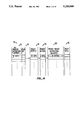
- FIG. 1 shows a prior art implementation of a branch prediction cache 12 and a pre-fetch instruction queue 14. Each of these is coupled between a system bus 16 and a processor 18. Each has its separate paths to the system bus and to the processor, respectively. When loading the pre-fetch instruction queue from the branch prediction cache, for example, the data must be transferred along the system bus or through the processor from the branch prediction cache to the pre-fetch instruction queue.
- FIG. 2 is a diagram of the present invention showing the integrated branch prediction cache and pre-fetch queue 20.
- This single structure is positioned between system bus 16 and processor 18 and requires only a single data path in each direction, rather than the multiple paths of FIG. 1.
- particular locations in the integrated structure are simply designated as a part of the queue dynamically.
- the entries are simply renamed.
- FIG. 3 illustrates what happens upon a branch.
- An entry in the BPC is pointed to as the target of the branch.
- the instruction words immediately following the entry are designated as the queue.
- the instruction pointed to could begin at different points within the entry.
- the second double word of the entry is at the beginning of the instruction, with the instruction being three double words long.
- the first double word of the queue is the last double word of the instruction.
- the entire instruction is loaded into the instruction buffer from the entry in the queue.
- the branch prediction cache is illustrated in FIG. 4. To understand FIG. 4, it is best to review what a branch instruction is.
- the instruction causing the change in control flow is called the "branch instruction”, and the address of this instruction is called the branch instruction address.
- the branch instruction may include within it the address of the instruction to be branched to, which is called the branch target instruction.
- the address of the branch target instruction is the "target address”. Alternately, a formula for calculating the target address may be included in the branch instruction.
- the branch instruction may be a conditional branch. A conditional branch causes a jump to a branch target instruction only if a test set forth in the branch instruction is met. If the condition is not met, then the branch is not taken and sequential execution continues.
- the branch prediction cache contains a number of columns.
- a first column 74 contains a tag which identifies the cache contents for a particular line. That tag is the branch instruction address itself.
- a separate column 76 contains a valid bit for each entry, indicating if the entry is valid.
- Another column 78 contains the target address pointed to by the branch instruction whose address is given in column 74. At least the first byte of the actual branch target instruction itself (possibly the entire instruction), possibly along with sequentially occurring instructions after the branch target instruction, up to 24 bytes total, is set forth in a column 80. Thus, the first useful instruction in the 24 bytes is located at the address pointed to by the target address of column 78.
- a column 82 contains valid bits for each of the instruction word blocks in column 80.
- a branch history column 84 contains two bits indicating the direction of the branch during the past executions of that branch instruction. For example, the possible arrangement of the two bits in column 4 could be as follows where the two choices of the conditional branch are A and B:
- FIGS. 5-10 show the BPC in more detail.
- FIG. 5 is a block diagram showing the various elements in BPC 152.
- the BPC comprises entries containing a relatively large amount of prediction information.
- this cache structure contains a full scope of information to enable single branch execution, including: the branch direction if the branch is conditional, the branch target address and cached target instruction data. More specifically, each cache line contains the target address from when the branch instruction was last executed; up to the first 24 bytes of sequential instruction stream starting at the target address; and two history bits recording the direction taken during past executions of the branch instruction.
- BPC 152 includes the branch address tag memory, called a program counter content addressable memory (PcCAM) 170 with associated valid bit (Vbit) memory 172.
- the target address memory is a branch address cache/target CAM (BAC/TgtCAM) 175.
- the history of past branch directions is in a branch history cache (BHC) 177.
- a branch target cache (BTC) 180 contains the target instruction data, with an associated target instruction valid (TIV) memory 182 storing valid bits for the instruction data in BTC 180.
- Each of the memory arrays contains 36 lines and is directly accessed via word select inputs (as opposed to encoded word address inputs). Some of these sets of word selects for reading and writing each line are generated by address selection logic 185 with associated multiplexer 188. Other word selects are generated by the match outputs of PcCAM 170.
- a Least Recently Used (LRU) logic block 181 has logic which performs the function of selecting a BPC line to be overwritten by a new block of instruction data.
- this cache Given the relatively limited size of this cache, it is designed to support accesses in a highly associative manner versus a direct-mapped or two/four-way set associative manner.
- This look-up to check whether an entry currently exists in the cache for a branch about to be processed, is typically performed using the address of the branch instruction. For some pipeline designs, a closely related address may instead need to be used.
- the term fully associative means that bits of the input address are compared with potentially matching bits of all the entries in cache. A hit is defined to have occurred when the input address matches at least one stored address.
- the term direct mapped means that some number of bits of the input address are used to index into the memory, and the remaining bits are stored in the memory. When the entry is read out of the memory, the stored address bits are compared with the corresponding bits in the input address, and a hit is defined to have occurred when the two agree. This entails a single comparison. In the event that two branch instructions index to the same entry (different PC's with the same set of bits), a direct mapped cache can only accommodate one, even if there are other empty entries.
- the term two-way set associative refers to a structure with two memory banks, so that two entries are read out for a given index and two comparisons are performed. This concept can be expanded to more than two-way set associative.
- the address of the first byte of the next instruction to be decoded is used for the look-up in the BPC, and is done in parallel with instruction fetch completion and start of instruction decode.
- This look-up is also done in a fully associative manner which provides substantial performance improvement relative to direct-mapped or two/four-way set-associative access methods.
- a cache tag for each entry namely the instruction address of the branch associated with the entry, is stored in PcCAM 170.
- a cache look-up is performed by accessing PcCAM 170 using the above next instruction address, and then reading out the prediction information from any, but at most one, entry for which there was a tag match.
- This greater associativity is with respect to both cache look-ups and cache replacements, i.e. when adding each entry to the cache a new entry to the cache requires that some other (hopefully less beneficial) entry be removed to make room.
- This greater flexibility in choosing "old" entries to be replaced by new entries it is statistically possible to better approximate the ideal of retaining prediction information for the branches deemed most likely to be processed again in the near future and the most often. In essence, full associativity maximizes the prediction cache's hit rate for a given cache size (in number of entries).
- An instruction buffer 153 (shown in FIG. 3) is used for temporarily holding instruction bytes before they are aligned and provided to the instruction register.
- Each logic schematic for one of the memories shows the circuitry for one line in that memory. Since there are 36 lines, in BPC 152, the circuitry shown for a given memory is repeated 36 times for that memory.
- FIG. 6 is a logic schematic of PcCAM 170 and associated Vbit memory 172.
- PcCAM 170 is a RAM/CAM array holding the instruction address of the branch for which each cache entry is storing prediction information.
- Each line in PcCAM 170 includes a 32-bit RAM word 190 and a CAM comparator 192.
- Each line in Vbit memory 172 holds a valid bit indicating the overall validity of the line, and is implemented as a latch 195.
- the CAM address input may be the address of the first byte of the next instruction to be decoded, and is compared with the contents of RAM word 190. In the event of equality, the CamMatch2 line for that entry is asserted, as qualified by a true output from Vbit latch 195.
- PcCAM 170 supports fully associative BPC lookups and replacements.
- the CamMatch2 signal from each line is output for use by the other BPC components, while the RAM aspect of the array applies only to writing instruction addresses into the PcCAM.
- FIG. 7 is a logic schematic of BAC/TgtCAM 175.
- the BAC/TgtCAM is a mixed RAM/CAM array holding the target address from the most recent execution.
- Each line includes a 39-bit RAM word 200, a 16-bit CAM comparator 207, a 4-bit CAM comparator 202, a pair of 7-bit CAM comparators 203 and 205, and associated logic.
- 39 bits 32 bits are the target address of the branch.
- the other 7 bits are additional target address information, as will be described below.
- the full 32-bit target address and the 2-bit history field are made available for readout if the particular BAC/TgtCAM line is selected, as determined by CamMatch2 from PcCAM 170 via mux 188.
- CAM segments of BAC/TgtCAM are used to detect memory stores by instructions currently being processed within the CPU pipeline or external writes or replacements. Since these instructions possibly modify target instruction bytes, it is necessary to invalidate the BPC entry in order to maintain proper coherency between target instruction bytes in the BTC and their image in main memory (actually in the ICache).
- ICache RAM chip 30 contains 64 kilobytes, organized as 32-byte lines, and is thus characterized by an 11-bit address (the five low order bits may be ignored).
- the ITAG RAM contains the high order 16 bits.
- the 27-bit address ChkAddr of a line being written in the ICache is communicated to the CamAddr1 input of the BAC/TgtCAM.
- the BTC entry could straddle a line boundary, and so may be characterized by two line addresses.
- two target addresses (which may be the same) need to be stored and checked.
- the high order 16 bits need not be checked for an external write, because the BPC is constrained to have only entries which are in the I cache for external writes.
- CAM comparators 203 and 205 compare the two 7-bit fields of the RAM line with the corresponding 7 bits of ChkAddr on the CAM Addr 1 input while CAM comparator 202 compares the 4-bit field in the RAM line with the corresponding 4 bits of ChkAddr.
- a match is defined to have occurred on a particular line if the 4 bits of the 27-bit ChkAddr match the 4 bits of the RAM line (as detected by comparator 202), the 7 bits of the ChkAddr match either 7-bit field of the RAM line (as detected by comparators 203 and 205) and the external write line is enabled or (for internal writes) the 16 bit field of ChkAddr matches the 16 bit field of the RAM line (as detected by comparator 207). If a match occurs (more than one can occur since more than one BTC entry can be affected by a write in a given line), the corresponding BPC entries are invalidated.
- the 32 bit branch target address can be read out through driver 204 on data bus rdBACData.
- FIG. 8 is a logic schematic of BTC 180.
- Each BTC slice comprises a 192-bit RAM word, implemented as three 64-bit RAM words (8 bytes) 220a, 220b, and 220c.
- the BTC possibly holds the first few instructions at the target address of the branch (in this case, up to the first 24 bytes of aligned target instruction data).
- the BTC cache caches the target instruction stream image as found in main memory.
- the first one or several target instructions could be cached in an alternate, possibly decoded, representation that may be more suitable for other CPU implementations.
- Each 64 bit output is provided through drivers 218a, 218b and 218c, with each RAM word output forming a 64 bit portion of 192 bit rdData output bus.
- the read select signal for a particular one of the 36 lines is provided through an AND gate 216.
- the write select signals are provided through a series of AND gates 214, 212 and 210.
- FIG. 9 is a logic schematic of TIV 182 and BHC 177.
- Each line of TIV 182 includes latches 225a, 225b, and 225c, each holding a valid bit corresponding to eight of the 24 instruction bytes within the BTC line.
- Each line of BHC 177 is a 2- bit RAM 127.
- FIG. 10 is a logic schematic of address select circuitry 185.
- Four pairs of latches designated IL1, FL1 through IL4, FL4 are provided.
- the first latch (IL) in each pair stores a pointer to an entry in the branch prediction cache.
- Four sets are provided to track multiple branches.
- the second latch (FL) in each pair is provided to point to a pre-fetch instruction queue which may be associated with each branch.
- One input to each of the IL latches is provided through multiplexers 240, 242, 244 and 246 from the PcCAM match line 248.
- Inputs to the FL latches are provided through a 36 bit input bus 252.
- the outputs of both the IL and the FL latches are provided to a multiplexing network 256.
- the circuit of FIG. 10 provides a flexible approach to producing a number of control signal outputs from the multiplexing network 256, as discussed below. For example, a PcCAM match will provide a 1 bit on one of the 36 bit lines, with all the rest being zero. This could be written into IL latch 1, for instance, so that a single bit in latch IL1 is enabled. The output could then be provided to multiplexing network 256 to activate the appropriate control lines for that entry.
- address select logic 185, PcCAM 170, and BAC/TgtCAM 175 provide various select and enable signals to control reading, writing, setting and clearing of addresses, instructions, and valid bits.
- the integrated BPC structure allows any number of these operations to be performed in the same cycle for different entries without contention of competing elements.
- a first access path, used to access the BPC entry, is invoked by communicating a 32-bit DecodePC signal to the CamAddr2 input of PcCAM 170. If a match occurs, a single bit of the 36-bit CamMatch2 output 248 is asserted, and is communicated to read select inputs on the other memory elements, namely BAC 175, BHC 177, BTC 180, and TIV 182 via mux 188. The result is that the corresponding entries, constituting the entire BPC entry, are read out of respective data outputs of the memory elements.
- a second access path used to clear an old entry and start a new entry, is invoked by writing a 36 bit word, with all 0's except for a single bit, which has a 1, into one of the latches of FIG. 10 through input 248 and multiplexers 240, 242, 244, and 246.
- the desired 32-bit address to be stored is provided to the WrData input of PcCAM 170 (see FIG. 5).
- the output 258 of multiplexer network 256 is selected to assert signals at the WrSe12 input of PcCAM 170, and the Clearza input of Vbit memory 172. This enables writing a new entry into the PcCAM, and clears the valid bit, pending acquisition of the target bytes.
- the same latch is used as a pointer for the BTC write, BAC write and BHC, V and TIV writes for that entry.
- One latch pair in address select logic 185 is a working latch pair which is not being used to track a particular branch at that time.
- the use of four sets of latches allows three instruction streams to be kept active (the original stream and two branches), while the fourth pair of latches is used for working purposes such as writing to PcCAM.
- the output of each FL latch, which is written to through address input 252, is also coupled back through the multiplexers 240-246 so that it can be written into the IL latch as desired.
- the FL is loaded for access (2), a write to PcCAM. It remains unchanged throughout (3)-(6) style accesses below if there is a hit. If there is a miss and an entry is created, then the FL is reloaded to point to a new queue. Accesses (3)-(6) may then occur.
- IL is loaded when there is a hit with the PcCAM output. It is then used for accesses (3)-(6).
- a third access path is used to fill in the BTC.
- the line is pointed to by the latch pointing to the PcCAM portion of the line.
- Three 8-byte select signals are provided to the WrEnx2 input of BTC 180.
- a single 8 byte block to be stored for the selected entry is provided to the WrData inputs on BTC 180. This allows part of a BTC entry to be written as multiplexer network 256 output 260 asserts select signals at inputs to the WrSe12 input of BTC 180.
- a fourth access path is used to write 39 bits of target address to the WrData inputs of BAC/TgtCAM 175 when the target address is available.
- a valid data bit is provided to the WrData input of Vbit memory 172, 3 bits are provided to TIV 182 and 2 bits of history information are provided to the WrData inputs of BHC 177. This allows completion of the BPC entry as output 262 of multiplexer network 256 is selected.
- a sixth data path is invoked by referencing one of the IL or FL latches as output 264 of multiplexing network 256.
- a select signal is also provided to multiplexer 188. This allows a given BTC and BAC line to be read out independently of any CAM hit from PcCAM 170. The entire BTC entry can be read, or one or more of the three double-words in the BTC entry can be read. This provides flexibility that allows certain otherwise unused BTC entries to be used for other purposes (such as instruction queues) and be controlled independently.
- a seventh access path is invoked by communicating ICache address information to the CAMAddr input of BAC/TgtCAM 175 for an external write to the I cache.
- the CAM portion of BAC/TgtCAM 175 performs the function of maintaining consistency between the target instruction bytes in BTC 180 and corresponding bytes in main memory (actually in the instruction cache).
- a match causes assertion of the appropriate CamMatch1 output line 266, and clears the corresponding Vbit.
- An eighth access path is invoked by asserting a signal at the ClearAll2 input 268 of Vbit 172. This can be carried out in a manner independent of other ongoing operations, and in some sense supercedes them all, because it invalidates all the BPC entries.
- the pre-fetch instruction queue is preferably implemented using one of the 36 entries of BTC 180 as shown in FIG. 11.
- a control state machine 56 keeps track of which of the 36 entries is the instruction queue. In fact, three entries are used for three queues in the preferred embodiment. In the event a conditional branch is encountered in one queue, that queue is retained while a separate queue for the predicted branch is set up and used. In case the predicted branch turns out to be a mispredicted direction, instruction execution can return to the first queue without having to rewrite it into the BTC. A third queue is provided in case there is a further conditional branch during execution of the second queue. This could result in 3 possible outstanding streams as shown in FIG. 12.
- Each queue contains three 8 byte blocks of instructions.
- the instruction words are provided in order on a 192 bit instruction bus 270 to instruction buffer 153.
- the words are then aligned by aligner 272 and are provided to instruction register 274 with the instruction aligned to start at the beginning of register 274.
- the instructions are then provided through an instruction pipeline 276, with each instruction being tagged and tracked as discussed earlier.
- Fetching down a queue wraps around and overwrites the three 8 byte blocks irrespective of the processing of the fetched instructions.
- An 8 byte block is free for overwriting (via a newly fetched block) as soon as the decoder has completely decoded all instructions contained in the block.
- one BTC line per active queue is allocated to serve as that queue, and during this time the (entire BPC) entry is marked as invalid insofar as BPC accesses are concerned.
- This is a dynamic assignment in that each time a new instruction stream is initiated and an instruction queue allocated for that stream, a BPC entry is assigned to be the new queue.
- a BPC entry which functions as a previous queue is used to avoid writing over active BPC entries.
- choice of entry is based on the same algorithm used during normal BPC replacements for selecting the "least useful in the future" entry.
- a modified instruction register or instruction buffer (This register is loaded from an instruction queue with the next instruction words to be decoded by the CPU's instruction decoder.) This register is expanded to be able to hold an entire copy of the current instruction queue instead of just a portion. As is explained below, this eliminates the need for an additional read access path out of the BTC RAM array.
- the integrated instruction queue/BTC is managed as follows. While the next instruction is being decoded, the address of this instruction is looked up in the BPC and an associative read access of the BTC is performed. If this instruction is, in fact, a control transfer and it "hits" in the BPC, then the contents of the accessed BTC entry is read out and loaded into the decoder's instruction register. This BTC entry effectively serves as an initial instruction queue for the target instruction.
- the decoder's instruction register is simply initialized empty and, as before, a new queue is allocated. Fetching of instructions is initiated from the target address, and received 8 byte blocks are loaded in parallel into both the new queue and the instruction register.
- this new queue is simply renamed or turned into a valid BPC entry. To ensure that this has the proper result, though, one constraint must be applied which in practice has insignificant performance impact. As this new queue is filled with target instruction blocks, they must all be retained even though the instruction decoder may already be finished referencing some of them.
- the queue must be frozen. This is in contrast to a normal queue, which is managed as a circular buffer with the oldest data being overwritten by new received data after the old data is no longer needed by the decoder.
- a further queue is not immediately allocated to support further fetching. Instead, fetching is suspended until a decision is made regarding whether or not to create a BPC entry for the transfer control instruction. If not, then either the existing "new" queue can proceed to function as a normal queue, or the target stream is not actually taken and the queue is simply deactivated. If so, then the BPC line that would have more conventionally been selected to be replaced (and to serve as the new entry), is invalidated and allocated as a replacement queue for the one being turned into the new BPC entry. Further instruction fetching then continues using this newest BTC line as a normal queue.
Abstract
Description
______________________________________
Bit Pattern   Branch History
______________________________________
00            AA
01            AB
10            BA
11            BB
______________________________________
Claims (5)
Priority Applications (3)
| Application Number | Priority Date | Filing Date | Title |
|---|---|---|---|
| US07/485,304 US5230068A (en) | 1990-02-26 | 1990-02-26 | Cache memory system for dynamically altering single cache memory line as either branch target entry or pre-fetch instruction queue based upon instruction sequence |
| PCT/US1991/000832 WO1991014224A1 (en) | 1990-02-26 | 1991-02-06 | Integrated instruction queue and branch target cache |
| US08/378,054 US5748932A (en) | 1990-02-26 | 1995-01-25 | Cache memory system for dynamically altering single cache memory line as either branch target entry or prefetch instruction queue based upon instruction sequence |
Applications Claiming Priority (1)
| Application Number | Priority Date | Filing Date | Title |
|---|---|---|---|
| US07/485,304 US5230068A (en) | 1990-02-26 | 1990-02-26 | Cache memory system for dynamically altering single cache memory line as either branch target entry or pre-fetch instruction queue based upon instruction sequence |
Related Child Applications (1)
| Application Number | Title | Priority Date | Filing Date |
|---|---|---|---|
| US6836493A Continuation | 1990-02-26 | 1993-05-27 |
Publications (1)
| Publication Number | Publication Date |
|---|---|
| US5230068A true US5230068A (en) | 1993-07-20 |
Family
ID=23927643
Family Applications (2)
| Application Number | Title | Priority Date | Filing Date |
|---|---|---|---|
| US07/485,304 Expired - Lifetime US5230068A (en) | 1990-02-26 | 1990-02-26 | Cache memory system for dynamically altering single cache memory line as either branch target entry or pre-fetch instruction queue based upon instruction sequence |
| US08/378,054 Expired - Lifetime US5748932A (en) | 1990-02-26 | 1995-01-25 | Cache memory system for dynamically altering single cache memory line as either branch target entry or prefetch instruction queue based upon instruction sequence |
Family Applications After (1)
| Application Number | Title | Priority Date | Filing Date |
|---|---|---|---|
| US08/378,054 Expired - Lifetime US5748932A (en) | 1990-02-26 | 1995-01-25 | Cache memory system for dynamically altering single cache memory line as either branch target entry or prefetch instruction queue based upon instruction sequence |
Country Status (2)
| Country | Link |
|---|---|
| US (2) | US5230068A (en) |
| WO (1) | WO1991014224A1 (en) |
Cited By (52)
| Publication number | Priority date | Publication date | Assignee | Title |
|---|---|---|---|---|
| US5353419A (en) * | 1992-01-09 | 1994-10-04 | Trustees Of The University Of Pennsylvania | Memory-side driven anticipatory instruction transfer interface with processor-side instruction selection |
| US5392417A (en) * | 1991-06-05 | 1995-02-21 | Intel Corporation | Processor cycle tracking in a controller for two-way set associative cache |
| US5418922A (en) * | 1992-04-30 | 1995-05-23 | International Business Machines Corporation | History table for set prediction for accessing a set associative cache |
| US5454117A (en) * | 1993-08-25 | 1995-09-26 | Nexgen, Inc. | Configurable branch prediction for a processor performing speculative execution |
| US5471597A (en) * | 1993-12-23 | 1995-11-28 | Unisys Corporation | System and method for executing branch instructions wherein branch target addresses are dynamically selectable under programmer control from writable branch address tables |
| US5504870A (en) * | 1991-04-22 | 1996-04-02 | Kabushiki Kaisha Toshiba | Branch prediction device enabling simultaneous access to a content-addressed memory for retrieval and registration |
| US5509130A (en) * | 1992-04-29 | 1996-04-16 | Sun Microsystems, Inc. | Method and apparatus for grouping multiple instructions, issuing grouped instructions simultaneously, and executing grouped instructions in a pipelined processor |
| US5515521A (en) * | 1994-02-08 | 1996-05-07 | Meridian Semiconductor, Inc. | Circuit and method for reducing delays associated with contention interference between code fetches and operand accesses of a microprocessor |
| US5553254A (en) * | 1993-01-15 | 1996-09-03 | International Business Machines Corporation | Instruction cache access and prefetch process controlled by a predicted instruction-path mechanism |
| US5584009A (en) * | 1993-10-18 | 1996-12-10 | Cyrix Corporation | System and method of retiring store data from a write buffer |
| US5586295A (en) * | 1993-01-21 | 1996-12-17 | Advanced Micro Devices, Inc. | Combination prefetch buffer and instruction cache |
| US5603045A (en) * | 1994-12-16 | 1997-02-11 | Vlsi Technology, Inc. | Microprocessor system having instruction cache with reserved branch target section |
| US5608886A (en) * | 1994-08-31 | 1997-03-04 | Exponential Technology, Inc. | Block-based branch prediction using a target finder array storing target sub-addresses |
| US5623614A (en) * | 1993-09-17 | 1997-04-22 | Advanced Micro Devices, Inc. | Branch prediction cache with multiple entries for returns having multiple callers |
| US5634103A (en) * | 1995-11-09 | 1997-05-27 | International Business Machines Corporation | Method and system for minimizing branch misprediction penalties within a processor |
| US5642493A (en) * | 1994-11-25 | 1997-06-24 | Motorola, Inc. | Method of loading instructions into an instruction cache by repetitively using a routine containing a mispredicted branch instruction |
| US5680565A (en) * | 1993-12-30 | 1997-10-21 | Intel Corporation | Method and apparatus for performing page table walks in a microprocessor capable of processing speculative instructions |
| US5724565A (en) * | 1995-02-03 | 1998-03-03 | International Business Machines Corporation | Method and system for processing first and second sets of instructions by first and second types of processing systems |
| US5737750A (en) * | 1994-08-31 | 1998-04-07 | Hewlett-Packard Company | Partitioned single array cache memory having first and second storage regions for storing non-branch and branch instructions |
| US5740417A (en) * | 1995-12-05 | 1998-04-14 | Motorola, Inc. | Pipelined processor operating in different power mode based on branch prediction state of branch history bit encoded as taken weakly not taken and strongly not taken states |
| US5751994A (en) * | 1990-08-06 | 1998-05-12 | Ncr Corporation | System and method for enhancing computer operation by prefetching data elements on a common bus without delaying bus access by multiple bus masters |
| US5764946A (en) * | 1995-04-12 | 1998-06-09 | Advanced Micro Devices | Superscalar microprocessor employing a way prediction unit to predict the way of an instruction fetch address and to concurrently provide a branch prediction address corresponding to the fetch address |
| US5784604A (en) * | 1992-10-09 | 1998-07-21 | International Business Machines Corporation | Method and system for reduced run-time delay during conditional branch execution in pipelined processor systems utilizing selectively delayed sequential instruction purging |
| US5794027A (en) * | 1993-07-01 | 1998-08-11 | International Business Machines Corporation | Method and apparatus for managing the execution of instructons with proximate successive branches in a cache-based data processing system |
| US5805877A (en) * | 1996-09-23 | 1998-09-08 | Motorola, Inc. | Data processor with branch target address cache and method of operation |
| US5812811A (en) * | 1995-02-03 | 1998-09-22 | International Business Machines Corporation | Executing speculative parallel instructions threads with forking and inter-thread communication |
| US5832259A (en) * | 1990-10-09 | 1998-11-03 | Advanced Micro Devices, Inc. | Apparatus for superscalar instruction pre-decoding using cached instruction lengths |
| US5848433A (en) * | 1995-04-12 | 1998-12-08 | Advanced Micro Devices | Way prediction unit and a method for operating the same |
| US5933860A (en) * | 1995-02-10 | 1999-08-03 | Digital Equipment Corporation | Multiprobe instruction cache with instruction-based probe hint generation and training whereby the cache bank or way to be accessed next is predicted |
| US5940857A (en) * | 1994-08-30 | 1999-08-17 | Mitsubishi Denki Kabushiki Kaisha | Instruction cache memory apparatus with advanced read function that predicts whether to read out a next instruction block including an address register, a counter and a selector |
| US5948100A (en) * | 1997-03-18 | 1999-09-07 | Industrial Technology Research Institute | Branch prediction and fetch mechanism for variable length instruction, superscalar pipelined processor |
| US5961629A (en) * | 1991-07-08 | 1999-10-05 | Seiko Epson Corporation | High performance, superscalar-based computer system with out-of-order instruction execution |
| US5974543A (en) * | 1998-01-23 | 1999-10-26 | International Business Machines Corporation | Apparatus and method for performing subroutine call and return operations |
| US5983334A (en) * | 1992-03-31 | 1999-11-09 | Seiko Epson Corporation | Superscalar microprocessor for out-of-order and concurrently executing at least two RISC instructions translating from in-order CISC instructions |
| US6016533A (en) * | 1997-12-16 | 2000-01-18 | Advanced Micro Devices, Inc. | Way prediction logic for cache array |
| US6038654A (en) * | 1991-07-08 | 2000-03-14 | Seiko Epson Corporation | High performance, superscalar-based computer system with out-of-order instruction execution |
| US6038653A (en) * | 1991-07-08 | 2000-03-14 | Seiko Epson Corporation | High-performance superscalar-based computer system with out-of-order instruction execution and concurrent results distribution |
| US6044449A (en) * | 1991-07-08 | 2000-03-28 | Seiko Epson Corporation | RISC microprocessor architecture implementing multiple typed register sets |
| US6073230A (en) * | 1997-06-11 | 2000-06-06 | Advanced Micro Devices, Inc. | Instruction fetch unit configured to provide sequential way prediction for sequential instruction fetches |
| US6092176A (en) * | 1992-12-31 | 2000-07-18 | Seiko Epson Corporation | System and method for assigning tags to control instruction processing in a superscalar processor |
| US6131157A (en) * | 1992-05-01 | 2000-10-10 | Seiko Epson Corporation | System and method for retiring approximately simultaneously a group of instructions in a superscalar microprocessor |
| US6138231A (en) * | 1992-12-31 | 2000-10-24 | Seiko Epson Corporation | System and method for register renaming |
| US6150724A (en) * | 1998-03-02 | 2000-11-21 | Motorola, Inc. | Multi-chip semiconductor device and method for making the device by using multiple flip chip interfaces |
| US6230254B1 (en) | 1992-09-29 | 2001-05-08 | Seiko Epson Corporation | System and method for handling load and/or store operators in a superscalar microprocessor |
| US6289433B1 (en) | 1992-03-31 | 2001-09-11 | Transmeta Corporation | Superscalar RISC instruction scheduling |
| US6304961B1 (en) | 1992-08-31 | 2001-10-16 | Sun Microsystems, Inc. | Computer system and method for fetching a next instruction |
| US6434693B1 (en) | 1992-09-29 | 2002-08-13 | Seiko Epson Corporation | System and method for handling load and/or store operations in a superscalar microprocessor |
| US20050050277A1 (en) * | 2003-09-03 | 2005-03-03 | Advanced Micro Devices, Inc. | MicroTLB and micro TAG for reducing power in a processor |
| US20050050278A1 (en) * | 2003-09-03 | 2005-03-03 | Advanced Micro Devices, Inc. | Low power way-predicted cache |
| US7673122B1 (en) | 2005-09-29 | 2010-03-02 | Sun Microsystems, Inc. | Software hint to specify the preferred branch prediction to use for a branch instruction |
| CN104391676A (en) * | 2014-11-10 | 2015-03-04 | 中国航天科技集团公司第九研究院第七七一研究所 | Instruction fetching method and instruction fetching structure thereof for low-cost high-band-width microprocessor |
| US20220283811A1 (en) * | 2021-03-03 | 2022-09-08 | Microsoft Technology Licensing, Llc | Loop buffering employing loop characteristic prediction in a processor for optimizing loop buffer performance |
Families Citing this family (6)
| Publication number | Priority date | Publication date | Assignee | Title |
|---|---|---|---|---|
| KR100240591B1 (en) * | 1996-11-06 | 2000-03-02 | 김영환 | Branch target buffer for processing branch instruction efficontly and brand prediction method using thereof |
| GB2381101B (en) * | 1998-04-20 | 2003-06-25 | Intel Corp | System and method for maintaining branch information |
| US6553488B2 (en) * | 1998-09-08 | 2003-04-22 | Intel Corporation | Method and apparatus for branch prediction using first and second level branch prediction tables |
| US8512134B2 (en) * | 2004-05-07 | 2013-08-20 | Dow K. Hardy | Method and apparatus for providing player incentives |
| US9317293B2 (en) * | 2012-11-28 | 2016-04-19 | Qualcomm Incorporated | Establishing a branch target instruction cache (BTIC) entry for subroutine returns to reduce execution pipeline bubbles, and related systems, methods, and computer-readable media |
| JP6016689B2 (en) * | 2013-03-28 | 2016-10-26 | ルネサスエレクトロニクス株式会社 | Semiconductor device |
Citations (32)
| Publication number | Priority date | Publication date | Assignee | Title |
|---|---|---|---|---|
| US4295193A (en) * | 1979-06-29 | 1981-10-13 | International Business Machines Corporation | Machine for multiple instruction execution |
| US4442488A (en) * | 1980-05-05 | 1984-04-10 | Floating Point Systems, Inc. | Instruction cache memory system |
| US4594659A (en) * | 1982-10-13 | 1986-06-10 | Honeywell Information Systems Inc. | Method and apparatus for prefetching instructions for a central execution pipeline unit |
| US4604691A (en) * | 1982-09-07 | 1986-08-05 | Nippon Electric Co., Ltd. | Data processing system having branch instruction prefetching performance |
| US4679141A (en) * | 1985-04-29 | 1987-07-07 | International Business Machines Corporation | Pageable branch history table |
| US4691277A (en) * | 1984-10-24 | 1987-09-01 | International Business Machines Corp. | Small instruction cache using branch target table to effect instruction prefetch |
| US4722050A (en) * | 1986-03-27 | 1988-01-26 | Hewlett-Packard Company | Method and apparatus for facilitating instruction processing of a digital computer |
| US4775955A (en) * | 1985-10-30 | 1988-10-04 | International Business Machines Corporation | Cache coherence mechanism based on locking |
| US4777594A (en) * | 1983-07-11 | 1988-10-11 | Prime Computer, Inc. | Data processing apparatus and method employing instruction flow prediction |
| US4777587A (en) * | 1985-08-30 | 1988-10-11 | Advanced Micro Devices, Inc. | System for processing single-cycle branch instruction in a pipeline having relative, absolute, indirect and trap addresses |
| US4796175A (en) * | 1986-08-27 | 1989-01-03 | Mitsubishi Denki Kabushiki Kaisha | Instruction fetching in data processing apparatus |
| US4802113A (en) * | 1983-11-11 | 1989-01-31 | Fujutsu Limited | Pipeline control system |
| US4827402A (en) * | 1985-04-22 | 1989-05-02 | Hitachi, Ltd. | Branch advanced control apparatus for advanced control of a branch instruction in a data processing system |
| US4847753A (en) * | 1986-10-07 | 1989-07-11 | Mitsubishi Denki K.K. | Pipelined computer |
| US4853840A (en) * | 1986-01-07 | 1989-08-01 | Nec Corporation | Instruction prefetching device including a circuit for checking prediction of a branch instruction before the instruction is executed |
| US4858104A (en) * | 1987-01-16 | 1989-08-15 | Mitsubishi Denki Kabushiki Kaisha | Preceding instruction address based branch prediction in a pipelined processor |
| US4860199A (en) * | 1987-07-31 | 1989-08-22 | Prime Computer, Inc. | Hashing indexer for branch cache |
| US4882673A (en) * | 1987-10-02 | 1989-11-21 | Advanced Micro Devices, Inc. | Method and apparatus for testing an integrated circuit including a microprocessor and an instruction cache |
| US4894772A (en) * | 1987-07-31 | 1990-01-16 | Prime Computer, Inc. | Method and apparatus for qualifying branch cache entries |
| US4926323A (en) * | 1988-03-03 | 1990-05-15 | Advanced Micro Devices, Inc. | Streamlined instruction processor |
| US4933837A (en) * | 1986-12-01 | 1990-06-12 | Advanced Micro Devices, Inc. | Methods and apparatus for optimizing instruction processing in computer systems employing a combination of instruction cache and high speed consecutive transfer memories |
| US4942520A (en) * | 1987-07-31 | 1990-07-17 | Prime Computer, Inc. | Method and apparatus for indexing, accessing and updating a memory |
| US4943908A (en) * | 1987-12-02 | 1990-07-24 | International Business Machines Corporation | Multiple branch analyzer for prefetching cache lines |
| US4984154A (en) * | 1982-11-17 | 1991-01-08 | Nec Corporation | Instruction prefetching device with prediction of a branch destination address |
| US4991080A (en) * | 1986-03-13 | 1991-02-05 | International Business Machines Corporation | Pipeline processing apparatus for executing instructions in three streams, including branch stream pre-execution processor for pre-executing conditional branch instructions |
| US4991078A (en) * | 1987-09-29 | 1991-02-05 | Digital Equipment Corporation | Apparatus and method for a pipelined central processing unit in a data processing system |
| US5072364A (en) * | 1989-05-24 | 1991-12-10 | Tandem Computers Incorporated | Method and apparatus for recovering from an incorrect branch prediction in a processor that executes a family of instructions in parallel |
| US5093778A (en) * | 1990-02-26 | 1992-03-03 | Nexgen Microsystems | Integrated single structure branch prediction cache |
| US5136697A (en) * | 1989-06-06 | 1992-08-04 | Advanced Micro Devices, Inc. | System for reducing delay for execution subsequent to correctly predicted branch instruction using fetch information stored with each block of instructions in cache |
| US5136696A (en) * | 1988-06-27 | 1992-08-04 | Prime Computer, Inc. | High-performance pipelined central processor for predicting the occurrence of executing single-cycle instructions and multicycle instructions |
| US5142634A (en) * | 1989-02-03 | 1992-08-25 | Digital Equipment Corporation | Branch prediction |
| US5163140A (en) * | 1990-02-26 | 1992-11-10 | Nexgen Microsystems | Two-level branch prediction cache |
Family Cites Families (22)
| Publication number | Priority date | Publication date | Assignee | Title |
|---|---|---|---|---|
| JPS549456B2 (en) * | 1972-07-05 | 1979-04-24 | ||
| US4521850A (en) * | 1977-12-30 | 1985-06-04 | Honeywell Information Systems Inc. | Instruction buffer associated with a cache memory unit |
| US4200927A (en) * | 1978-01-03 | 1980-04-29 | International Business Machines Corporation | Multi-instruction stream branch processing mechanism |
| US4287561A (en) * | 1978-03-16 | 1981-09-01 | International Business Machines Corporation | Address formulation interlock mechanism |
| US4430706A (en) * | 1980-10-27 | 1984-02-07 | Burroughs Corporation | Branch prediction apparatus and method for a data processing system |
| US4477872A (en) * | 1982-01-15 | 1984-10-16 | International Business Machines Corporation | Decode history table for conditional branch instructions |
| US4521851A (en) * | 1982-10-13 | 1985-06-04 | Honeywell Information Systems Inc. | Central processor |
| US4631660A (en) * | 1983-08-30 | 1986-12-23 | Amdahl Corporation | Addressing system for an associative cache memory |
| JPS6051948A (en) * | 1983-08-31 | 1985-03-23 | Hitachi Ltd | Branch destination buffer storage device |
| JPS60168238A (en) * | 1984-02-10 | 1985-08-31 | Hitachi Ltd | Instruction control system |
| US4742451A (en) * | 1984-05-21 | 1988-05-03 | Digital Equipment Corporation | Instruction prefetch system for conditional branch instruction for central processor unit |
| US4714994A (en) * | 1985-04-30 | 1987-12-22 | International Business Machines Corp. | Instruction prefetch buffer control |
| US4763245A (en) * | 1985-10-30 | 1988-08-09 | International Business Machines Corporation | Branch prediction mechanism in which a branch history table is updated using an operand sensitive branch table |
| DE3785897T2 (en) * | 1986-02-28 | 1993-09-30 | Nec Corp | CONTROL DEVICE FOR PRELIMINARY COMMANDS. |
| JPS6393041A (en) * | 1986-10-07 | 1988-04-23 | Mitsubishi Electric Corp | Computer |
| US4860197A (en) * | 1987-07-31 | 1989-08-22 | Prime Computer, Inc. | Branch cache system with instruction boundary determination independent of parcel boundary |
| US4905188A (en) * | 1988-02-22 | 1990-02-27 | International Business Machines Corporation | Functional cache memory chip architecture for improved cache access |
| US4974155A (en) * | 1988-08-15 | 1990-11-27 | Evans & Sutherland Computer Corp. | Variable delay branch system |
| US5101341A (en) * | 1988-08-25 | 1992-03-31 | Edgcore Technology, Inc. | Pipelined system for reducing instruction access time by accumulating predecoded instruction bits a FIFO |
| US5050068A (en) * | 1988-10-03 | 1991-09-17 | Duke University | Method and apparatus for using extracted program flow information to prepare for execution multiple instruction streams |
| JPH0769811B2 (en) * | 1988-12-21 | 1995-07-31 | 松下電器産業株式会社 | Data processing device |
| US5127091A (en) * | 1989-01-13 | 1992-06-30 | International Business Machines Corporation | System for reducing delay in instruction execution by executing branch instructions in separate processor while dispatching subsequent instructions to primary processor |
-
1990
- 1990-02-26 US US07/485,304 patent/US5230068A/en not_active Expired - Lifetime
-
1991
- 1991-02-06 WO PCT/US1991/000832 patent/WO1991014224A1/en unknown
-
1995
- 1995-01-25 US US08/378,054 patent/US5748932A/en not_active Expired - Lifetime
Patent Citations (32)
| Publication number | Priority date | Publication date | Assignee | Title |
|---|---|---|---|---|
| US4295193A (en) * | 1979-06-29 | 1981-10-13 | International Business Machines Corporation | Machine for multiple instruction execution |
| US4442488A (en) * | 1980-05-05 | 1984-04-10 | Floating Point Systems, Inc. | Instruction cache memory system |
| US4604691A (en) * | 1982-09-07 | 1986-08-05 | Nippon Electric Co., Ltd. | Data processing system having branch instruction prefetching performance |
| US4594659A (en) * | 1982-10-13 | 1986-06-10 | Honeywell Information Systems Inc. | Method and apparatus for prefetching instructions for a central execution pipeline unit |
| US4984154A (en) * | 1982-11-17 | 1991-01-08 | Nec Corporation | Instruction prefetching device with prediction of a branch destination address |
| US4777594A (en) * | 1983-07-11 | 1988-10-11 | Prime Computer, Inc. | Data processing apparatus and method employing instruction flow prediction |
| US4802113A (en) * | 1983-11-11 | 1989-01-31 | Fujutsu Limited | Pipeline control system |
| US4691277A (en) * | 1984-10-24 | 1987-09-01 | International Business Machines Corp. | Small instruction cache using branch target table to effect instruction prefetch |
| US4827402A (en) * | 1985-04-22 | 1989-05-02 | Hitachi, Ltd. | Branch advanced control apparatus for advanced control of a branch instruction in a data processing system |
| US4679141A (en) * | 1985-04-29 | 1987-07-07 | International Business Machines Corporation | Pageable branch history table |
| US4777587A (en) * | 1985-08-30 | 1988-10-11 | Advanced Micro Devices, Inc. | System for processing single-cycle branch instruction in a pipeline having relative, absolute, indirect and trap addresses |
| US4775955A (en) * | 1985-10-30 | 1988-10-04 | International Business Machines Corporation | Cache coherence mechanism based on locking |
| US4853840A (en) * | 1986-01-07 | 1989-08-01 | Nec Corporation | Instruction prefetching device including a circuit for checking prediction of a branch instruction before the instruction is executed |
| US4991080A (en) * | 1986-03-13 | 1991-02-05 | International Business Machines Corporation | Pipeline processing apparatus for executing instructions in three streams, including branch stream pre-execution processor for pre-executing conditional branch instructions |
| US4722050A (en) * | 1986-03-27 | 1988-01-26 | Hewlett-Packard Company | Method and apparatus for facilitating instruction processing of a digital computer |
| US4796175A (en) * | 1986-08-27 | 1989-01-03 | Mitsubishi Denki Kabushiki Kaisha | Instruction fetching in data processing apparatus |
| US4847753A (en) * | 1986-10-07 | 1989-07-11 | Mitsubishi Denki K.K. | Pipelined computer |
| US4933837A (en) * | 1986-12-01 | 1990-06-12 | Advanced Micro Devices, Inc. | Methods and apparatus for optimizing instruction processing in computer systems employing a combination of instruction cache and high speed consecutive transfer memories |
| US4858104A (en) * | 1987-01-16 | 1989-08-15 | Mitsubishi Denki Kabushiki Kaisha | Preceding instruction address based branch prediction in a pipelined processor |
| US4860199A (en) * | 1987-07-31 | 1989-08-22 | Prime Computer, Inc. | Hashing indexer for branch cache |
| US4894772A (en) * | 1987-07-31 | 1990-01-16 | Prime Computer, Inc. | Method and apparatus for qualifying branch cache entries |
| US4942520A (en) * | 1987-07-31 | 1990-07-17 | Prime Computer, Inc. | Method and apparatus for indexing, accessing and updating a memory |
| US4991078A (en) * | 1987-09-29 | 1991-02-05 | Digital Equipment Corporation | Apparatus and method for a pipelined central processing unit in a data processing system |
| US4882673A (en) * | 1987-10-02 | 1989-11-21 | Advanced Micro Devices, Inc. | Method and apparatus for testing an integrated circuit including a microprocessor and an instruction cache |
| US4943908A (en) * | 1987-12-02 | 1990-07-24 | International Business Machines Corporation | Multiple branch analyzer for prefetching cache lines |
| US4926323A (en) * | 1988-03-03 | 1990-05-15 | Advanced Micro Devices, Inc. | Streamlined instruction processor |
| US5136696A (en) * | 1988-06-27 | 1992-08-04 | Prime Computer, Inc. | High-performance pipelined central processor for predicting the occurrence of executing single-cycle instructions and multicycle instructions |
| US5142634A (en) * | 1989-02-03 | 1992-08-25 | Digital Equipment Corporation | Branch prediction |
| US5072364A (en) * | 1989-05-24 | 1991-12-10 | Tandem Computers Incorporated | Method and apparatus for recovering from an incorrect branch prediction in a processor that executes a family of instructions in parallel |
| US5136697A (en) * | 1989-06-06 | 1992-08-04 | Advanced Micro Devices, Inc. | System for reducing delay for execution subsequent to correctly predicted branch instruction using fetch information stored with each block of instructions in cache |
| US5093778A (en) * | 1990-02-26 | 1992-03-03 | Nexgen Microsystems | Integrated single structure branch prediction cache |
| US5163140A (en) * | 1990-02-26 | 1992-11-10 | Nexgen Microsystems | Two-level branch prediction cache |
Non-Patent Citations (6)
| Title |
|---|
| A. Thampy Thomas; "A Single Cycle VLSI CISC-Based Workstation: System Overview and Performance Characteristics"; Computer Society of the IEEE; pp. 500-503. |
| A. Thampy Thomas; A Single Cycle VLSI CISC Based Workstation: System Overview and Performance Characteristics ; Computer Society of the IEEE; pp. 500 503. * |
| Atig Raza; "Technology Constraints on VLSI Processor Implementation"; Computer Society of the Thirty-Fourth IEEE; pp. 509-512. |
| Atig Raza; Technology Constraints on VLSI Processor Implementation ; Computer Society of the Thirty Fourth IEEE; pp. 509 512. * |
| David R. Stiles and Harold L. McFarland; "Piperline Control for a Single Cycle VLSI Implementation of a Complex Instruction Set Computer"; Computer Society of the IEEE; pp. 504-508. |
| David R. Stiles and Harold L. McFarland; Piperline Control for a Single Cycle VLSI Implementation of a Complex Instruction Set Computer ; Computer Society of the IEEE; pp. 504 508. * |
Cited By (136)
| Publication number | Priority date | Publication date | Assignee | Title |
|---|---|---|---|---|
| US5751994A (en) * | 1990-08-06 | 1998-05-12 | Ncr Corporation | System and method for enhancing computer operation by prefetching data elements on a common bus without delaying bus access by multiple bus masters |
| US5832259A (en) * | 1990-10-09 | 1998-11-03 | Advanced Micro Devices, Inc. | Apparatus for superscalar instruction pre-decoding using cached instruction lengths |
| US5504870A (en) * | 1991-04-22 | 1996-04-02 | Kabushiki Kaisha Toshiba | Branch prediction device enabling simultaneous access to a content-addressed memory for retrieval and registration |
| US5392417A (en) * | 1991-06-05 | 1995-02-21 | Intel Corporation | Processor cycle tracking in a controller for two-way set associative cache |
| US6948052B2 (en) | 1991-07-08 | 2005-09-20 | Seiko Epson Corporation | High-performance, superscalar-based computer system with out-of-order instruction execution |
| US7739482B2 (en) | 1991-07-08 | 2010-06-15 | Seiko Epson Corporation | High-performance, superscalar-based computer system with out-of-order instruction execution |
| US6934829B2 (en) | 1991-07-08 | 2005-08-23 | Seiko Epson Corporation | High-performance, superscalar-based computer system with out-of-order instruction execution |
| US6256720B1 (en) | 1991-07-08 | 2001-07-03 | Seiko Epson Corporation | High performance, superscalar-based computer system with out-of-order instruction execution |
| US6915412B2 (en) | 1991-07-08 | 2005-07-05 | Seiko Epson Corporation | High-performance, superscalar-based computer system with out-of-order instruction execution |
| US7721070B2 (en) | 1991-07-08 | 2010-05-18 | Le Trong Nguyen | High-performance, superscalar-based computer system with out-of-order instruction execution |
| US7685402B2 (en) | 1991-07-08 | 2010-03-23 | Sanjiv Garg | RISC microprocessor architecture implementing multiple typed register sets |
| US6249856B1 (en) | 1991-07-08 | 2001-06-19 | Seiko Epson Corporation | RISC microprocessor architecture implementing multiple typed register sets |
| US7555632B2 (en) | 1991-07-08 | 2009-06-30 | Seiko Epson Corporation | High-performance superscalar-based computer system with out-of-order instruction execution and concurrent results distribution |
| US7555631B2 (en) | 1991-07-08 | 2009-06-30 | Sanjiv Garg | RISC microprocessor architecture implementing multiple typed register sets |
| US7487333B2 (en) | 1991-07-08 | 2009-02-03 | Seiko Epson Corporation | High-performance, superscalar-based computer system with out-of-order instruction execution |
| US6272619B1 (en) | 1991-07-08 | 2001-08-07 | Seiko Epson Corporation | High-performance, superscalar-based computer system with out-of-order instruction execution |
| US6282630B1 (en) | 1991-07-08 | 2001-08-28 | Seiko Epson Corporation | High-performance, superscalar-based computer system with out-of-order instruction execution and concurrent results distribution |
| US20070101103A1 (en) * | 1991-07-08 | 2007-05-03 | Nguyen Le T | High-performance superscalar-based computer system with out-of order instruction execution and concurrent results distribution |
| US7162610B2 (en) | 1991-07-08 | 2007-01-09 | Seiko Epson Corporation | High-performance, superscalar-based computer system with out-of-order instruction execution |
| US20040093482A1 (en) * | 1991-07-08 | 2004-05-13 | Seiko Epson Corporation | High-performance, superscalar-based computer system with out-of-order instruction execution |
| US7941636B2 (en) | 1991-07-08 | 2011-05-10 | Intellectual Venture Funding Llc | RISC microprocessor architecture implementing multiple typed register sets |
| US20020016903A1 (en) * | 1991-07-08 | 2002-02-07 | Nguyen Le Trong | High-performance, superscalar-based computer system with out-of-order instruction execution and concurrent results distribution |
| US6986024B2 (en) | 1991-07-08 | 2006-01-10 | Seiko Epson Corporation | High-performance, superscalar-based computer system with out-of-order instruction execution |
| US6959375B2 (en) | 1991-07-08 | 2005-10-25 | Seiko Epson Corporation | High-performance, superscalar-based computer system with out-of-order instruction execution |
| US6128723A (en) * | 1991-07-08 | 2000-10-03 | Seiko Epson Corporation | High-performance, superscalar-based computer system with out-of-order instruction execution |
| US20030056086A1 (en) * | 1991-07-08 | 2003-03-20 | Le Trong Nguyen | High-performance, superscalar-based computer system with out-of-order instruction execution |
| US6941447B2 (en) | 1991-07-08 | 2005-09-06 | Seiko Epson Corporation | High-performance, superscalar-based computer system with out-of-order instruction execution |
| US6101594A (en) * | 1991-07-08 | 2000-08-08 | Seiko Epson Corporation | High-performance, superscalar-based computer system with out-of-order instruction execution |
| US20030079113A1 (en) * | 1991-07-08 | 2003-04-24 | Nguyen Le Trong | High-performance, superscalar-based computer system with out-of-order instruction execution |
| US7941635B2 (en) | 1991-07-08 | 2011-05-10 | Seiko-Epson Corporation | High-performance superscalar-based computer system with out-of order instruction execution and concurrent results distribution |
| US6092181A (en) * | 1991-07-08 | 2000-07-18 | Seiko Epson Corporation | High-performance, superscalar-based computer system with out-of-order instruction execution |
| US20040093485A1 (en) * | 1991-07-08 | 2004-05-13 | Seiko Epson Corporation | High-performance, superscalar-based computer system with out-of-order instruction execution |
| US5961629A (en) * | 1991-07-08 | 1999-10-05 | Seiko Epson Corporation | High performance, superscalar-based computer system with out-of-order instruction execution |
| US20040093483A1 (en) * | 1991-07-08 | 2004-05-13 | Seiko Epson Corporation | High performance, superscalar-based computer system with out-of-order instruction execution |
| US20030115440A1 (en) * | 1991-07-08 | 2003-06-19 | Sanjiv Garg | RISC microprocessor architecture implementing multiple typed register sets |
| US20040054872A1 (en) * | 1991-07-08 | 2004-03-18 | Seiko Epson Corporation | High-performance, superscalar-based computer system with out-of-order intstruction execution |
| US6647485B2 (en) | 1991-07-08 | 2003-11-11 | Seiko Epson Corporation | High-performance, superscalar-based computer system with out-of-order instruction execution |
| US6038654A (en) * | 1991-07-08 | 2000-03-14 | Seiko Epson Corporation | High performance, superscalar-based computer system with out-of-order instruction execution |
| US6038653A (en) * | 1991-07-08 | 2000-03-14 | Seiko Epson Corporation | High-performance superscalar-based computer system with out-of-order instruction execution and concurrent results distribution |
| US6044449A (en) * | 1991-07-08 | 2000-03-28 | Seiko Epson Corporation | RISC microprocessor architecture implementing multiple typed register sets |
| US5353419A (en) * | 1992-01-09 | 1994-10-04 | Trustees Of The University Of Pennsylvania | Memory-side driven anticipatory instruction transfer interface with processor-side instruction selection |
| US6289433B1 (en) | 1992-03-31 | 2001-09-11 | Transmeta Corporation | Superscalar RISC instruction scheduling |
| US7051187B2 (en) | 1992-03-31 | 2006-05-23 | Transmeta Corporation | Superscalar RISC instruction scheduling |
| US5983334A (en) * | 1992-03-31 | 1999-11-09 | Seiko Epson Corporation | Superscalar microprocessor for out-of-order and concurrently executing at least two RISC instructions translating from in-order CISC instructions |
| US6954847B2 (en) | 1992-03-31 | 2005-10-11 | Transmeta Corporation | System and method for translating non-native instructions to native instructions for processing on a host processor |
| US6263423B1 (en) | 1992-03-31 | 2001-07-17 | Seiko Epson Corporation | System and method for translating non-native instructions to native instructions for processing on a host processor |
| US20060041736A1 (en) * | 1992-03-31 | 2006-02-23 | Transmeta Corporation | Superscalar RISC instruction scheduling |
| US20030084270A1 (en) * | 1992-03-31 | 2003-05-01 | Transmeta Corp. | System and method for translating non-native instructions to native instructions for processing on a host processor |
| US7343473B2 (en) | 1992-03-31 | 2008-03-11 | Transmeta Corporation | System and method for translating non-native instructions to native instructions for processing on a host processor |
| US20080162880A1 (en) * | 1992-03-31 | 2008-07-03 | Transmeta Corporation | System and Method for Translating Non-Native Instructions to Native Instructions for Processing on a Host Processor |
| US7664935B2 (en) | 1992-03-31 | 2010-02-16 | Brett Coon | System and method for translating non-native instructions to native instructions for processing on a host processor |
| US7802074B2 (en) | 1992-03-31 | 2010-09-21 | Sanjiv Garg | Superscalar RISC instruction scheduling |
| US5509130A (en) * | 1992-04-29 | 1996-04-16 | Sun Microsystems, Inc. | Method and apparatus for grouping multiple instructions, issuing grouped instructions simultaneously, and executing grouped instructions in a pipelined processor |
| US5418922A (en) * | 1992-04-30 | 1995-05-23 | International Business Machines Corporation | History table for set prediction for accessing a set associative cache |
| US20020178347A1 (en) * | 1992-05-01 | 2002-11-28 | Johannes Wang | System and method for retiring approximately simultaneously a group of instructions in a superscalar microprocessor |
| US6412064B1 (en) | 1992-05-01 | 2002-06-25 | Seiko Epson Corporation | System and method for retiring approximately simultaneously a group of instructions in a superscalar microprocessor |
| US6920548B2 (en) | 1992-05-01 | 2005-07-19 | Seiko Epson Corporation | System and method for retiring approximately simultaneously a group of instructions in a superscalar microprocessor |
| US20040186983A1 (en) * | 1992-05-01 | 2004-09-23 | Seiko Epson Corporation | System and method for retiring approximately simultaneously a group of instructions in a superscalar microprocessor |
| US20070106880A1 (en) * | 1992-05-01 | 2007-05-10 | Johannes Wang | System and method for retiring approximately simultaneously a group of instructions in a superscalar microprocessor |
| US6131157A (en) * | 1992-05-01 | 2000-10-10 | Seiko Epson Corporation | System and method for retiring approximately simultaneously a group of instructions in a superscalar microprocessor |
| US7934078B2 (en) | 1992-05-01 | 2011-04-26 | Seiko Epson Corporation | System and method for retiring approximately simultaneously a group of instructions in a superscalar microprocessor |
| US7958337B2 (en) | 1992-05-01 | 2011-06-07 | Seiko Epson Corporation | System and method for retiring approximately simultaneously a group of instructions in a superscalar microprocessor |
| US6304961B1 (en) | 1992-08-31 | 2001-10-16 | Sun Microsystems, Inc. | Computer system and method for fetching a next instruction |
| US20040128487A1 (en) * | 1992-09-29 | 2004-07-01 | Seiko Epson Corporation | System and method for handling load and/or store operations in a superscalar microprocessor |
| US6230254B1 (en) | 1992-09-29 | 2001-05-08 | Seiko Epson Corporation | System and method for handling load and/or store operators in a superscalar microprocessor |
| US6957320B2 (en) | 1992-09-29 | 2005-10-18 | Seiko Epson Corporation | System and method for handling load and/or store operations in a superscalar microprocessor |
| US6434693B1 (en) | 1992-09-29 | 2002-08-13 | Seiko Epson Corporation | System and method for handling load and/or store operations in a superscalar microprocessor |
| US8019975B2 (en) | 1992-09-29 | 2011-09-13 | Seiko-Epson Corporation | System and method for handling load and/or store operations in a superscalar microprocessor |
| US20020188829A1 (en) * | 1992-09-29 | 2002-12-12 | Senter Cheryl D. | System and method for handling load and/or store operations in a superscalar microprocessor |
| US20070101106A1 (en) * | 1992-09-29 | 2007-05-03 | Senter Cheryl D | System and method for handling load and/or store operations in a superscalar microprocessor |
| US20030056089A1 (en) * | 1992-09-29 | 2003-03-20 | Seiko Epson Corporation | System and method for handling load and/or store operations in a superscalar microprocessor |
| US20090217001A1 (en) * | 1992-09-29 | 2009-08-27 | Seiko Epson Corporation | System and Method for Handling Load and/or Store Operations in a Superscalar Microprocessor |
| US20050283591A1 (en) * | 1992-09-29 | 2005-12-22 | Seiko Epson Corporation | System and method for handling load and/or store operations in a superscalar microprocessor |
| US7000097B2 (en) | 1992-09-29 | 2006-02-14 | Seiko Epson Corporation | System and method for handling load and/or store operations in a superscalar microprocessor |
| US7447876B2 (en) | 1992-09-29 | 2008-11-04 | Seiko Epson Corporation | System and method for handling load and/or store operations in a superscalar microprocessor |
| US6965987B2 (en) | 1992-09-29 | 2005-11-15 | Seiko Epson Corporation | System and method for handling load and/or store operations in a superscalar microprocessor |
| US6735685B1 (en) | 1992-09-29 | 2004-05-11 | Seiko Epson Corporation | System and method for handling load and/or store operations in a superscalar microprocessor |
| US7844797B2 (en) | 1992-09-29 | 2010-11-30 | Seiko Epson Corporation | System and method for handling load and/or store operations in a superscalar microprocessor |
| US7861069B2 (en) | 1992-09-29 | 2010-12-28 | Seiko-Epson Corporation | System and method for handling load and/or store operations in a superscalar microprocessor |
| US5784604A (en) * | 1992-10-09 | 1998-07-21 | International Business Machines Corporation | Method and system for reduced run-time delay during conditional branch execution in pipelined processor systems utilizing selectively delayed sequential instruction purging |
| US7430651B2 (en) | 1992-12-31 | 2008-09-30 | Seiko-Epson Corporation | System and method for assigning tags to control instruction processing in a superscalar processor |
| US6922772B2 (en) | 1992-12-31 | 2005-07-26 | Seiko Epson Corporation | System and method for register renaming |
| US8074052B2 (en) | 1992-12-31 | 2011-12-06 | Seiko Epson Corporation | System and method for assigning tags to control instruction processing in a superscalar processor |
| US20040199746A1 (en) * | 1992-12-31 | 2004-10-07 | Seiko Epson Corporation | System and method for assigning tags to control instruction processing in a superscalar processor |
| US6360309B1 (en) | 1992-12-31 | 2002-03-19 | Seiko Epson Corporation | System and method for assigning tags to control instruction processing in a superscalar processor |
| US20060123218A1 (en) * | 1992-12-31 | 2006-06-08 | Seiko Epson Corporation | System and method for assigning tags to control instruction processing in a superscalar processor |
| US6138231A (en) * | 1992-12-31 | 2000-10-24 | Seiko Epson Corporation | System and method for register renaming |
| US7043624B2 (en) | 1992-12-31 | 2006-05-09 | Seiko Epson Corporation | System and method for assigning tags to control instruction processing in a superscalar processor |
| US6408375B2 (en) | 1992-12-31 | 2002-06-18 | Seiko Epson Corporation | System and method for register renaming |
| US20060020773A1 (en) * | 1992-12-31 | 2006-01-26 | Seiko Epson Corporation | System and method for register renaming |
| US6757808B2 (en) | 1992-12-31 | 2004-06-29 | Seiko Epson Corporation | System and method for assigning tags to control instruction processing in a superscalar processor |
| US6092176A (en) * | 1992-12-31 | 2000-07-18 | Seiko Epson Corporation | System and method for assigning tags to control instruction processing in a superscalar processor |
| US7979678B2 (en) | 1992-12-31 | 2011-07-12 | Seiko Epson Corporation | System and method for register renaming |
| US20020083300A1 (en) * | 1992-12-31 | 2002-06-27 | Deosaran Trevor A. | System and method for register renaming |
| US6970995B2 (en) | 1992-12-31 | 2005-11-29 | Seiko Epson Corporation | System and method for register renaming |
| US5553254A (en) * | 1993-01-15 | 1996-09-03 | International Business Machines Corporation | Instruction cache access and prefetch process controlled by a predicted instruction-path mechanism |
| US5586295A (en) * | 1993-01-21 | 1996-12-17 | Advanced Micro Devices, Inc. | Combination prefetch buffer and instruction cache |
| US5794027A (en) * | 1993-07-01 | 1998-08-11 | International Business Machines Corporation | Method and apparatus for managing the execution of instructons with proximate successive branches in a cache-based data processing system |
| US5454117A (en) * | 1993-08-25 | 1995-09-26 | Nexgen, Inc. | Configurable branch prediction for a processor performing speculative execution |
| US5815699A (en) * | 1993-08-25 | 1998-09-29 | Advanced Micro Devices, Inc. | Configurable branch prediction for a processor performing speculative execution |
| US6282639B1 (en) | 1993-08-25 | 2001-08-28 | Advanced Micro Devices, Inc. | Configurable branch prediction for a processor performing speculative execution |
| US6108777A (en) * | 1993-08-25 | 2000-08-22 | Advanced Micro Devices, Inc. | Configurable branch prediction for a processor performing speculative execution |
| US6360318B1 (en) | 1993-08-25 | 2002-03-19 | Advanced Micro Devices, Inc. | Configurable branch prediction for a processor performing speculative execution |
| US5623614A (en) * | 1993-09-17 | 1997-04-22 | Advanced Micro Devices, Inc. | Branch prediction cache with multiple entries for returns having multiple callers |
| US5584009A (en) * | 1993-10-18 | 1996-12-10 | Cyrix Corporation | System and method of retiring store data from a write buffer |
| US5471597A (en) * | 1993-12-23 | 1995-11-28 | Unisys Corporation | System and method for executing branch instructions wherein branch target addresses are dynamically selectable under programmer control from writable branch address tables |
| US5680565A (en) * | 1993-12-30 | 1997-10-21 | Intel Corporation | Method and apparatus for performing page table walks in a microprocessor capable of processing speculative instructions |
| US5515521A (en) * | 1994-02-08 | 1996-05-07 | Meridian Semiconductor, Inc. | Circuit and method for reducing delays associated with contention interference between code fetches and operand accesses of a microprocessor |
| US5940857A (en) * | 1994-08-30 | 1999-08-17 | Mitsubishi Denki Kabushiki Kaisha | Instruction cache memory apparatus with advanced read function that predicts whether to read out a next instruction block including an address register, a counter and a selector |
| US5608886A (en) * | 1994-08-31 | 1997-03-04 | Exponential Technology, Inc. | Block-based branch prediction using a target finder array storing target sub-addresses |
| US5737750A (en) * | 1994-08-31 | 1998-04-07 | Hewlett-Packard Company | Partitioned single array cache memory having first and second storage regions for storing non-branch and branch instructions |
| US5642493A (en) * | 1994-11-25 | 1997-06-24 | Motorola, Inc. | Method of loading instructions into an instruction cache by repetitively using a routine containing a mispredicted branch instruction |
| US5603045A (en) * | 1994-12-16 | 1997-02-11 | Vlsi Technology, Inc. | Microprocessor system having instruction cache with reserved branch target section |
| US5724565A (en) * | 1995-02-03 | 1998-03-03 | International Business Machines Corporation | Method and system for processing first and second sets of instructions by first and second types of processing systems |
| US5812811A (en) * | 1995-02-03 | 1998-09-22 | International Business Machines Corporation | Executing speculative parallel instructions threads with forking and inter-thread communication |
| US5933860A (en) * | 1995-02-10 | 1999-08-03 | Digital Equipment Corporation | Multiprobe instruction cache with instruction-based probe hint generation and training whereby the cache bank or way to be accessed next is predicted |
| US5764946A (en) * | 1995-04-12 | 1998-06-09 | Advanced Micro Devices | Superscalar microprocessor employing a way prediction unit to predict the way of an instruction fetch address and to concurrently provide a branch prediction address corresponding to the fetch address |
| US5848433A (en) * | 1995-04-12 | 1998-12-08 | Advanced Micro Devices | Way prediction unit and a method for operating the same |
| US5634103A (en) * | 1995-11-09 | 1997-05-27 | International Business Machines Corporation | Method and system for minimizing branch misprediction penalties within a processor |
| US5740417A (en) * | 1995-12-05 | 1998-04-14 | Motorola, Inc. | Pipelined processor operating in different power mode based on branch prediction state of branch history bit encoded as taken weakly not taken and strongly not taken states |
| US5805877A (en) * | 1996-09-23 | 1998-09-08 | Motorola, Inc. | Data processor with branch target address cache and method of operation |
| US5948100A (en) * | 1997-03-18 | 1999-09-07 | Industrial Technology Research Institute | Branch prediction and fetch mechanism for variable length instruction, superscalar pipelined processor |
| US6035387A (en) * | 1997-03-18 | 2000-03-07 | Industrial Technology Research Institute | System for packing variable length instructions into fixed length blocks with indications of instruction beginning, ending, and offset within block |
| US6101595A (en) * | 1997-06-11 | 2000-08-08 | Advanced Micro Devices, Inc. | Fetching instructions from an instruction cache using sequential way prediction |
| US6073230A (en) * | 1997-06-11 | 2000-06-06 | Advanced Micro Devices, Inc. | Instruction fetch unit configured to provide sequential way prediction for sequential instruction fetches |
| US6115792A (en) * | 1997-12-16 | 2000-09-05 | Advanced Micro Devices, Inc. | Way prediction logic for cache array |
| US6016533A (en) * | 1997-12-16 | 2000-01-18 | Advanced Micro Devices, Inc. | Way prediction logic for cache array |
| US5974543A (en) * | 1998-01-23 | 1999-10-26 | International Business Machines Corporation | Apparatus and method for performing subroutine call and return operations |
| US6150724A (en) * | 1998-03-02 | 2000-11-21 | Motorola, Inc. | Multi-chip semiconductor device and method for making the device by using multiple flip chip interfaces |
| US20050050277A1 (en) * | 2003-09-03 | 2005-03-03 | Advanced Micro Devices, Inc. | MicroTLB and micro TAG for reducing power in a processor |
| US20050050278A1 (en) * | 2003-09-03 | 2005-03-03 | Advanced Micro Devices, Inc. | Low power way-predicted cache |
| US7117290B2 (en) | 2003-09-03 | 2006-10-03 | Advanced Micro Devices, Inc. | MicroTLB and micro tag for reducing power in a processor |
| US7673122B1 (en) | 2005-09-29 | 2010-03-02 | Sun Microsystems, Inc. | Software hint to specify the preferred branch prediction to use for a branch instruction |
| CN104391676A (en) * | 2014-11-10 | 2015-03-04 | 中国航天科技集团公司第九研究院第七七一研究所 | Instruction fetching method and instruction fetching structure thereof for low-cost high-band-width microprocessor |
| CN104391676B (en) * | 2014-11-10 | 2017-11-10 | 中国航天科技集团公司第九研究院第七七一研究所 | The microprocessor fetching method and its fetching structure of a kind of inexpensive high bandwidth |
| US20220283811A1 (en) * | 2021-03-03 | 2022-09-08 | Microsoft Technology Licensing, Llc | Loop buffering employing loop characteristic prediction in a processor for optimizing loop buffer performance |
Also Published As
| Publication number | Publication date |
|---|---|
| US5748932A (en) | 1998-05-05 |
| WO1991014224A1 (en) | 1991-09-19 |
Similar Documents
| Publication | Publication Date | Title |
|---|---|---|
| US5230068A (en) | Cache memory system for dynamically altering single cache memory line as either branch target entry or pre-fetch instruction queue based upon instruction sequence | |
| US5093778A (en) | Integrated single structure branch prediction cache | |
| US5781924A (en) | Computer caching methods and apparatus | |
| US5918245A (en) | Microprocessor having a cache memory system using multi-level cache set prediction | |
| US5226130A (en) | Method and apparatus for store-into-instruction-stream detection and maintaining branch prediction cache consistency | |
| US6425075B1 (en) | Branch prediction device with two levels of branch prediction cache | |
| US5551001A (en) | Master-slave cache system for instruction and data cache memories | |
| USRE45078E1 (en) | Highly efficient design of storage array utilizing multiple pointers to indicate valid and invalid lines for use in first and second cache spaces and memory subsystems | |
| US6412043B1 (en) | Microprocessor having improved memory management unit and cache memory | |
| EP0734553B1 (en) | Split level cache | |
| US5761712A (en) | Data memory unit and method for storing data into a lockable cache in one clock cycle by previewing the tag array | |
| US5381533A (en) | Dynamic flow instruction cache memory organized around trace segments independent of virtual address line | |
| US7707397B2 (en) | Variable group associativity branch target address cache delivering multiple target addresses per cache line | |
| US6598128B1 (en) | Microprocessor having improved memory management unit and cache memory | |
| US5793941A (en) | On-chip primary cache testing circuit and test method | |
| US6678815B1 (en) | Apparatus and method for reducing power consumption due to cache and TLB accesses in a processor front-end | |
| US5715427A (en) | Semi-associative cache with MRU/LRU replacement | |
| US6012134A (en) | High-performance processor with streaming buffer that facilitates prefetching of instructions | |
| US9753855B2 (en) | High-performance instruction cache system and method | |
| US20030074530A1 (en) | Load/store unit with fast memory data access mechanism | |
| US5649137A (en) | Method and apparatus for store-into-instruction-stream detection and maintaining branch prediction cache consistency | |
| US5155828A (en) | Computing system with a cache memory and an additional look-aside cache memory | |
| US5909566A (en) | Microprocessor circuits, systems, and methods for speculatively executing an instruction using its most recently used data while concurrently prefetching data for the instruction | |
| US5574883A (en) | Single chip processing unit providing immediate availability of frequently used microcode instruction words | |
| US6553460B1 (en) | Microprocessor having improved memory management unit and cache memory |
Legal Events
| Date | Code | Title | Description |
|---|---|---|---|
| AS | Assignment |
Owner name: NEXGEN MICROSYSTEMS, A CORP. OF CALIFORNIA, CALIFO Free format text: ASSIGNMENT OF ASSIGNORS INTEREST.;ASSIGNORS:VAN DYKE, KORBIN S.;FAVOR, JOHN G.;REEL/FRAME:005285/0825;SIGNING DATES FROM 19900409 TO 19900417 |
|
| STCF | Information on status: patent grant |
Free format text: PATENTED CASE |
|
| AS | Assignment |
Owner name: PHEMUS CORPORATION, MASSACHUSETTS Free format text: SECURITY INTEREST;ASSIGNOR:NEXGEN MICROSYSTEMS, INC.;REEL/FRAME:006801/0513 Effective date: 19930722 |
|
| AS | Assignment |
Owner name: ADVANCED MICRO DEVICES, INC., CALIFORNIA Free format text: SECURITY INTEREST;ASSIGNOR:NEXGEN, INC., A DELAWARE CORPORATION;REEL/FRAME:007696/0914 Effective date: 19951020 |
|
| AS | Assignment |
Owner name: NEXGEN, INC., CALIFORNIA Free format text: CHANGE OF NAME;ASSIGNOR:NEXGEN MICROSYSTEMS;REEL/FRAME:007696/0073 Effective date: 19940526 |
|
| FEPP | Fee payment procedure |
Free format text: PAT HLDR NO LONGER CLAIMS SMALL ENT STAT AS SMALL BUSINESS (ORIGINAL EVENT CODE: LSM2); ENTITY STATUS OF PATENT OWNER: LARGE ENTITY |
|
| AS | Assignment |
Owner name: SILICON VALLEY BANK, CALIFORNIA Free format text: RELEASE;ASSIGNOR:NEXGEN MICROSYSTEMS;REEL/FRAME:007767/0158 Effective date: 19920403 |
|
| FEPP | Fee payment procedure |
Free format text: PAYOR NUMBER ASSIGNED (ORIGINAL EVENT CODE: ASPN); ENTITY STATUS OF PATENT OWNER: LARGE ENTITY |
|
| FPAY | Fee payment |
Year of fee payment: 4 |
|
| FPAY | Fee payment |
Year of fee payment: 8 |
|
| FPAY | Fee payment |
Year of fee payment: 12 |