US5238713A - Spin-on method and apparatus for applying coating material to a substrate, including an air flow developing and guiding step/means - Google Patents
Spin-on method and apparatus for applying coating material to a substrate, including an air flow developing and guiding step/means Download PDFInfo
- Publication number
- US5238713A US5238713A US07/792,635 US79263591A US5238713A US 5238713 A US5238713 A US 5238713A US 79263591 A US79263591 A US 79263591A US 5238713 A US5238713 A US 5238713A
- Authority
- US
- United States
- Prior art keywords
- substrate
- coating material
- air
- air flow
- flow
- Prior art date
- Legal status (The legal status is an assumption and is not a legal conclusion. Google has not performed a legal analysis and makes no representation as to the accuracy of the status listed.)
- Expired - Lifetime
Links
Images


Classifications
-
- H—ELECTRICITY
- H01—ELECTRIC ELEMENTS
- H01L—SEMICONDUCTOR DEVICES NOT COVERED BY CLASS H10
- H01L21/00—Processes or apparatus adapted for the manufacture or treatment of semiconductor or solid state devices or of parts thereof
- H01L21/67—Apparatus specially adapted for handling semiconductor or electric solid state devices during manufacture or treatment thereof; Apparatus specially adapted for handling wafers during manufacture or treatment of semiconductor or electric solid state devices or components ; Apparatus not specifically provided for elsewhere
- H01L21/67005—Apparatus not specifically provided for elsewhere
- H01L21/67011—Apparatus for manufacture or treatment
- H01L21/6715—Apparatus for applying a liquid, a resin, an ink or the like
Definitions
- This invention relates to methods and apparatus for applying a coating material such as a photoresist masking material to a substrate such as a semiconductor wafer or glass.
- Japanese utility model publication No. 60-95979 open to public inspection on Jun. 29, 1985, discloses an automated spin coater which includes an enclosure within which a spinner chuck is supported for rotation by a motor.
- the spinner chuck has a vacuum table on which a semiconductor wafer is securely held by vacuum action.
- a photoresist coating material is applied to the semiconductor wafer which is spun to coat it evenly by centrifugal forces.
- a coating material is likely to be deposited at corners of the substrate due to wind pressure. Such undesirable deposition or uneven coating on the substrate may subsequently result in malfunctions during further processing or use of the substrate and therefore, may also result in a serious decrease in the yield of acceptably coated substrates.
- an object of the invention to provide a method and apparatus for applying a coating material to a substrate, wherein an even coating can be provided over the entire surface of the substrate.
- a method for applying a coating material to a substrate comprising the steps of spinning the substrate, applying the coating material onto the surface of the substrate, and developing and guiding a flow of air over the substrate primarily in a direction identical to the direction of rotation of the substrate.
- an apparatus for applying a coating material to a substrate which comprises an enclosure, a spinning chuck rotatably supported within the enclosure and having a vacuum table on which the substrate is securely held, means for applying the coating material onto the surface of the substrate, means for developing a flow of air over the substrate, and means for guiding the flow of air primarily in a direction identical to the direction of rotation of the substrate.
- the air guide means includes an annular air duct disposed in surrounding and spaced relation to the spinning chuck, and a fixed disk disposed between the air duct and the spinning chuck and having a plurality of guide vanes thereon.
- the flow of air is developed by fans mounted within the air duct and guided by the guide vanes, to eliminate undesirable deposition from the end edge or periphery of the substrate.
- the flow of air may alternatively be developed by a vacuum system having vacuum lines adapted to connect the air duct with vacuum sources.
- FIG. 1 is a vertical section of a coating apparatus designed in accordance with the principles of the invention
- FIG. 2 is a schematic plan view of a semiconductive substrate, showing how a coating liquid as applied thereto flows when the substrate is rotated;
- FIG. 3 is a sectional view taken along the line III--III of FIG. 2.
- FIG. 4 is a schematic plan view of the coating apparatus with a cover removed for clarity.
- FIG. 5 is a view similar to FIG. 4, but showing a modification
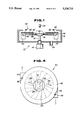
- FIG. 1 there is shown a coating apparatus or automatic spin coater indicated generally by the numeral 10 and having an enclosure 12. Centrally disposed within the enclosure 12 is a spinning chuck 14 which is connected for rotation by an electric motor 16. A vacuum table 18 is fixed at its center to the spinning chuck 14 and also, coupled to a vacuum source (not shown) to thereby securely hold a square semiconductive or silicon substrate 20 thereon. Upon energization of the motor 16, the vacuum table 18, together with the semiconductive substrate 20, is rotated at a rate in the range of 1000 to 6000 rpm.
- the enclosure 12 is centrally open as at 22 through which a photoresist masking material, or other coating material is applied to the top surface of the semiconductive substrate 20 by a nozzle 24 of a conventional dispensing device. Liquid residues as radially broadcast by centrifugal forces flow out of the enclosure 12 through a drainage outlet 26.
- a coating or masking material spread to the edge of the substrate by centrifugal forces, can be ejected from the periphery of the substrate in a direction tangentially of the substrate. This provides even coating over the entire surface of the substrate. When the square substrate is used, this is not the case.
- a coating material 28 spread to the edge of the substrate 20 flows in a direction (arrow 31) opposite to the direction of rotation of the substrate (arrow 32) along its side edges and then travels in a direction as indicated by arrow 33. This results in an undesirable deposition or formation of raised portions 34 at each corner of the substrate 20 (see FIG. 3).
- an air guide assembly as indicated generally by the numeral 40.
- an annular air duct 42 is located circumferentially about and spaced from the vacuum table 18 and has diametrically opposite outlets 44,44.
- Fans 46,46 are mounted in the air duct 42 adjacent to the outlets 44,44, respectively and are driven by suitable drive means, such as electric motors (not shown) to develop adequate air flow over the substrate 20.
- a fixed disk 48 Situated between the air duct 42 and the vacuum table 18 is a fixed disk 48 on which a plurality of, preferably 15 to 16 guides vanes or fins 50.
- the fixed disk 48 is centrally open to permit access of the vacuum table 18 to the enclosure 12.
- the guide vanes 50 extend in a direction tangentially of the vacuum table 18.
- a cover 52 is provided over the guide vanes 50 and the air duct 42.
- the substrate 20 is either manually or automatically loaded centrally on the vacuum table 18 and is pulled into mating engagement with the vacuum table 18 by vacuum action.
- the photoresist masking material is then applied to the top surface of the substrate 20 by the nozzle 24.
- the motor 16 is energized to spin the vacuum table 18, together with the substrate 20 securely held thereon, in a direction as shown by arrow 53 in FIG. 4.
- a centrifugal flow component is imparted to the liquid masking material causing it to spread over the top surface of the substrate 20.
- the motors are energized to rotate the fans 46,46 to develop air flow over the substrate 20, the air flowing from the center to the end edges of the substrate 20 primarily in a direction identical to the direction of rotation of the substrate 20 as shown by arrow 56.
- This air flow serves to eject undesirable deposition from the end edges of the substrate 20 so as to provide even coating over the entire surface of the substrate 20.
- a vacuum system 60 may alternatively be provided, in place of the fans 46,46 shown in FIG. 4.
- the vacuum system 60 includes two separate vacuum lines 61 adapted to connect the outlets 44 with two corresponding vacuum sources 62 through vacuum controllers 63. Similar air flow, as indicated by arrow 65, is developed by vacuum action so as to eject undesirable deposition from the end edges of the substrate 20.
Abstract
A coating apparatus comprises a spinning chuck rotatably supported within an enclosure and securely holding a substrate thereon. A coating material is applied onto the surface of the substrate and distributed over the substrate by centrifugal forces. An annular air duct is disposed in surrounding and spaced relation to the spinning chuck, and a disk is placed between the air duct and the spinning chuck and has a plurality of guide vanes. Fans are provided in the air duct to develop a positive flow of air over the substrate. The flow of air is guided by the guide vanes in a direction identical to the direction of rotation of the substrate so as to eliminate undesirable deposition from the end edges of the substrate.
Description
This application is a continuation of copending U.S. patent application Ser. No. 07/246,403, filed Sep. 19, 1988 (now U.S. Pat. No. 5,116,250).
1. Field of the Invention
This invention relates to methods and apparatus for applying a coating material such as a photoresist masking material to a substrate such as a semiconductor wafer or glass.
2. Description of the Related Art
Japanese utility model publication No. 60-95979, open to public inspection on Jun. 29, 1985, discloses an automated spin coater which includes an enclosure within which a spinner chuck is supported for rotation by a motor. The spinner chuck has a vacuum table on which a semiconductor wafer is securely held by vacuum action. A photoresist coating material is applied to the semiconductor wafer which is spun to coat it evenly by centrifugal forces.
When a substrate to be coated is of a shape other than round, a coating material is likely to be deposited at corners of the substrate due to wind pressure. Such undesirable deposition or uneven coating on the substrate may subsequently result in malfunctions during further processing or use of the substrate and therefore, may also result in a serious decrease in the yield of acceptably coated substrates.
It is, therefore, an object of the invention to provide a method and apparatus for applying a coating material to a substrate, wherein an even coating can be provided over the entire surface of the substrate.
According to one aspect of the invention, there is provided a method for applying a coating material to a substrate, comprising the steps of spinning the substrate, applying the coating material onto the surface of the substrate, and developing and guiding a flow of air over the substrate primarily in a direction identical to the direction of rotation of the substrate.
According to another aspect of the invention, there is provided an apparatus for applying a coating material to a substrate, which comprises an enclosure, a spinning chuck rotatably supported within the enclosure and having a vacuum table on which the substrate is securely held, means for applying the coating material onto the surface of the substrate, means for developing a flow of air over the substrate, and means for guiding the flow of air primarily in a direction identical to the direction of rotation of the substrate.
In a preferred embodiment, the air guide means includes an annular air duct disposed in surrounding and spaced relation to the spinning chuck, and a fixed disk disposed between the air duct and the spinning chuck and having a plurality of guide vanes thereon. The flow of air is developed by fans mounted within the air duct and guided by the guide vanes, to eliminate undesirable deposition from the end edge or periphery of the substrate. The flow of air may alternatively be developed by a vacuum system having vacuum lines adapted to connect the air duct with vacuum sources.
A better understanding of the invention may be had by reference to the following description of preferred embodiments when taken in conjunction with the accompanying drawings; in which:
FIG. 1 is a vertical section of a coating apparatus designed in accordance with the principles of the invention;
FIG. 2 is a schematic plan view of a semiconductive substrate, showing how a coating liquid as applied thereto flows when the substrate is rotated;
FIG. 3 is a sectional view taken along the line III--III of FIG. 2.
FIG. 4 is a schematic plan view of the coating apparatus with a cover removed for clarity; and
FIG. 5 is a view similar to FIG. 4, but showing a modification;
Referring now to the drawings and first to FIG. 1, there is shown a coating apparatus or automatic spin coater indicated generally by the numeral 10 and having an enclosure 12. Centrally disposed within the enclosure 12 is a spinning chuck 14 which is connected for rotation by an electric motor 16. A vacuum table 18 is fixed at its center to the spinning chuck 14 and also, coupled to a vacuum source (not shown) to thereby securely hold a square semiconductive or silicon substrate 20 thereon. Upon energization of the motor 16, the vacuum table 18, together with the semiconductive substrate 20, is rotated at a rate in the range of 1000 to 6000 rpm. The enclosure 12 is centrally open as at 22 through which a photoresist masking material, or other coating material is applied to the top surface of the semiconductive substrate 20 by a nozzle 24 of a conventional dispensing device. Liquid residues as radially broadcast by centrifugal forces flow out of the enclosure 12 through a drainage outlet 26.
When a substrate is circular in shape, a coating or masking material, spread to the edge of the substrate by centrifugal forces, can be ejected from the periphery of the substrate in a direction tangentially of the substrate. This provides even coating over the entire surface of the substrate. When the square substrate is used, this is not the case. As shown in FIG. 2, a coating material 28, spread to the edge of the substrate 20, flows in a direction (arrow 31) opposite to the direction of rotation of the substrate (arrow 32) along its side edges and then travels in a direction as indicated by arrow 33. This results in an undesirable deposition or formation of raised portions 34 at each corner of the substrate 20 (see FIG. 3).
In order to eliminate such undesirable deposition and provide even coating over the entire surface of the substrate, there is provided an air guide assembly as indicated generally by the numeral 40. Specifically, an annular air duct 42 is located circumferentially about and spaced from the vacuum table 18 and has diametrically opposite outlets 44,44. Fans 46,46 are mounted in the air duct 42 adjacent to the outlets 44,44, respectively and are driven by suitable drive means, such as electric motors (not shown) to develop adequate air flow over the substrate 20. Situated between the air duct 42 and the vacuum table 18 is a fixed disk 48 on which a plurality of, preferably 15 to 16 guides vanes or fins 50. The fixed disk 48 is centrally open to permit access of the vacuum table 18 to the enclosure 12. Illustratively, the guide vanes 50 extend in a direction tangentially of the vacuum table 18. A cover 52 is provided over the guide vanes 50 and the air duct 42.
In use, the substrate 20 is either manually or automatically loaded centrally on the vacuum table 18 and is pulled into mating engagement with the vacuum table 18 by vacuum action. The photoresist masking material is then applied to the top surface of the substrate 20 by the nozzle 24. Thereafter, the motor 16 is energized to spin the vacuum table 18, together with the substrate 20 securely held thereon, in a direction as shown by arrow 53 in FIG. 4. A centrifugal flow component is imparted to the liquid masking material causing it to spread over the top surface of the substrate 20. At the same time, the motors are energized to rotate the fans 46,46 to develop air flow over the substrate 20, the air flowing from the center to the end edges of the substrate 20 primarily in a direction identical to the direction of rotation of the substrate 20 as shown by arrow 56. This air flow serves to eject undesirable deposition from the end edges of the substrate 20 so as to provide even coating over the entire surface of the substrate 20.
With reference to FIG. 5, a vacuum system 60 may alternatively be provided, in place of the fans 46,46 shown in FIG. 4. Common elements in FIGS. 4 and 5 have the same identifying numerals. Illustratively, the vacuum system 60 includes two separate vacuum lines 61 adapted to connect the outlets 44 with two corresponding vacuum sources 62 through vacuum controllers 63. Similar air flow, as indicated by arrow 65, is developed by vacuum action so as to eject undesirable deposition from the end edges of the substrate 20.
While the invention has been described with respect to preferred embodiments, further modifications may be made without departing from the scope and spirit of the invention. It is intended to cover such modifications as fall within the scope of the appended claims.
Claims (7)
1. A method for applying a coating material to a substrate, comprising the steps of:
spinning a substrate;
applying a liquid coating material onto a surface of the substrate;
developing and guiding a flow of air over the substrate primarily in a direction identical to the direction of rotation of the substrate so as to assist in ejecting the coating material from edge portions of the substrate
said air flow developing and guiding step being achieved independently of said substrate spinning step.
2. A method according to claim 1, wherein said substrate is polygonal in shape.
3. A method according to claim 2, wherein said substrate is square.
4. An apparatus for applying a coating material to a substrate, comprising:
means for supporting a substrate within a enclosure;
means for spinning the substrate;
means for applying a liquid coating material onto a surface of the substrate;
means for developing a flow of air over the substrate;
means for guiding the flow of air primarily in a direction identical to the direction of rotation of the substrate so as to assist in ejecting the coating material from edge portions of the substrate and
said air flow developing means and said air flow guiding means being independent of said substrate and said substrate spinning means.
5. Apparatus according to claim 2, wherein said substrate is polygonal in shape.
6. Apparatus according to claim 5, wherein said substrate is square.
7. Apparatus according to claim 2, wherein said air flow developing means and said air flow guiding means are disposed radially outwardly of the substrate in surrounding relation thereto.
Priority Applications (1)
| Application Number | Priority Date | Filing Date | Title |
|---|---|---|---|
| US07/792,635 US5238713A (en) | 1987-09-18 | 1991-11-15 | Spin-on method and apparatus for applying coating material to a substrate, including an air flow developing and guiding step/means |
Applications Claiming Priority (4)
| Application Number | Priority Date | Filing Date | Title |
|---|---|---|---|
| JP62234054A JPH0829287B2 (en) | 1987-09-18 | 1987-09-18 | Coating method and device |
| JP62-234054 | 1987-09-18 | ||
| US07/246,403 US5116250A (en) | 1987-09-18 | 1988-09-19 | Method and apparatus for applying a coating material to a substrate |
| US07/792,635 US5238713A (en) | 1987-09-18 | 1991-11-15 | Spin-on method and apparatus for applying coating material to a substrate, including an air flow developing and guiding step/means |
Related Parent Applications (1)
| Application Number | Title | Priority Date | Filing Date |
|---|---|---|---|
| US07/246,403 Continuation US5116250A (en) | 1987-09-18 | 1988-09-19 | Method and apparatus for applying a coating material to a substrate |
Publications (1)
| Publication Number | Publication Date |
|---|---|
| US5238713A true US5238713A (en) | 1993-08-24 |
Family
ID=27332071
Family Applications (1)
| Application Number | Title | Priority Date | Filing Date |
|---|---|---|---|
| US07/792,635 Expired - Lifetime US5238713A (en) | 1987-09-18 | 1991-11-15 | Spin-on method and apparatus for applying coating material to a substrate, including an air flow developing and guiding step/means |
Country Status (1)
| Country | Link |
|---|---|
| US (1) | US5238713A (en) |
Cited By (18)
| Publication number | Priority date | Publication date | Assignee | Title |
|---|---|---|---|---|
| US5472502A (en) * | 1993-08-30 | 1995-12-05 | Semiconductor Systems, Inc. | Apparatus and method for spin coating wafers and the like |
| US5474807A (en) * | 1992-09-30 | 1995-12-12 | Hoya Corporation | Method for applying or removing coatings at a confined peripheral region of a substrate |
| US5688555A (en) * | 1996-06-03 | 1997-11-18 | Taiwan Semiconductor Manufacturing Company Ltd | Gas barrier during edge rinse of SOG coating process to prevent SOG hump formation |
| US5705223A (en) * | 1994-07-26 | 1998-01-06 | International Business Machine Corp. | Method and apparatus for coating a semiconductor wafer |
| US5743965A (en) * | 1995-08-30 | 1998-04-28 | Origin Electric Company, Limited | Disk coating system |
| US5861061A (en) * | 1996-06-21 | 1999-01-19 | Micron Technology, Inc. | Spin coating bowl |
| US5952050A (en) * | 1996-02-27 | 1999-09-14 | Micron Technology, Inc. | Chemical dispensing system for semiconductor wafer processing |
| US6068881A (en) * | 1998-05-29 | 2000-05-30 | International Business Machines Corporation | Spin-apply tool having exhaust ring |
| US6140253A (en) * | 1996-07-16 | 2000-10-31 | Micron Technology, Inc. | Spin coating bowl |
| US6261635B1 (en) * | 1999-08-27 | 2001-07-17 | Micron Technology, Inc. | Method for controlling air over a spinning microelectronic substrate |
| US20020004100A1 (en) * | 1994-10-27 | 2002-01-10 | Emir Gurer | Method of uniformly coating a substrate |
| US6417117B1 (en) | 1996-06-21 | 2002-07-09 | Micron Technology, Inc. | Spin coating spindle and chuck assembly |
| US6672318B1 (en) * | 1999-09-09 | 2004-01-06 | Mimasu Semiconductor Industry Co., Ltd. | Wafer rotary holding apparatus and wafer surface treatment apparatus with waste liquid recovery mechanism |
| US7018943B2 (en) | 1994-10-27 | 2006-03-28 | Asml Holding N.V. | Method of uniformly coating a substrate |
| US7030039B2 (en) | 1994-10-27 | 2006-04-18 | Asml Holding N.V. | Method of uniformly coating a substrate |
| US20100189913A1 (en) * | 2008-12-03 | 2010-07-29 | The Regents Of The University Of Michigan Office Of Technology Transfer | Rolling contact layer-by-layer assembly |
| US8795783B2 (en) | 2009-08-31 | 2014-08-05 | The Regents Of The University Of Michigan | Preparation of layer-by-layer materials and coatings from ionic liquids |
| US20170342604A1 (en) * | 2014-12-22 | 2017-11-30 | Rieter Ingolstadt Gmbh | Rotor Spinning Machine Comprising a Plurality of Working Positions and a Suction Device |
Citations (6)
| Publication number | Priority date | Publication date | Assignee | Title |
|---|---|---|---|---|
| US4068019A (en) * | 1976-11-08 | 1978-01-10 | International Business Machines Corporation | Spin coating process for prevention of edge buildup |
| US4374873A (en) * | 1979-11-07 | 1983-02-22 | Phenix Works Societe Anonyme | Process and installation for coating a metallic strip continuously with a covering layer |
| US4393807A (en) * | 1979-09-19 | 1983-07-19 | Fujitsu Limited | Spinner |
| US4510176A (en) * | 1983-09-26 | 1985-04-09 | At&T Bell Laboratories | Removal of coating from periphery of a semiconductor wafer |
| JPS6095979A (en) * | 1983-10-31 | 1985-05-29 | Semiconductor Energy Lab Co Ltd | Production of photoelectric conversion semiconductor device |
| US4528934A (en) * | 1981-02-16 | 1985-07-16 | Tokyo Denshi Kagaku Kabushiki Kaisha | Thin-film coating apparatus |
-
1991
- 1991-11-15 US US07/792,635 patent/US5238713A/en not_active Expired - Lifetime
Patent Citations (6)
| Publication number | Priority date | Publication date | Assignee | Title |
|---|---|---|---|---|
| US4068019A (en) * | 1976-11-08 | 1978-01-10 | International Business Machines Corporation | Spin coating process for prevention of edge buildup |
| US4393807A (en) * | 1979-09-19 | 1983-07-19 | Fujitsu Limited | Spinner |
| US4374873A (en) * | 1979-11-07 | 1983-02-22 | Phenix Works Societe Anonyme | Process and installation for coating a metallic strip continuously with a covering layer |
| US4528934A (en) * | 1981-02-16 | 1985-07-16 | Tokyo Denshi Kagaku Kabushiki Kaisha | Thin-film coating apparatus |
| US4510176A (en) * | 1983-09-26 | 1985-04-09 | At&T Bell Laboratories | Removal of coating from periphery of a semiconductor wafer |
| JPS6095979A (en) * | 1983-10-31 | 1985-05-29 | Semiconductor Energy Lab Co Ltd | Production of photoelectric conversion semiconductor device |
Cited By (29)
| Publication number | Priority date | Publication date | Assignee | Title |
|---|---|---|---|---|
| US5474807A (en) * | 1992-09-30 | 1995-12-12 | Hoya Corporation | Method for applying or removing coatings at a confined peripheral region of a substrate |
| US5869211A (en) * | 1992-09-30 | 1999-02-09 | Hoya Corporation | Phase shift mask blank having a coated central shading pattern and uncoated peripheral portion |
| US5472502A (en) * | 1993-08-30 | 1995-12-05 | Semiconductor Systems, Inc. | Apparatus and method for spin coating wafers and the like |
| US5705223A (en) * | 1994-07-26 | 1998-01-06 | International Business Machine Corp. | Method and apparatus for coating a semiconductor wafer |
| US20020004100A1 (en) * | 1994-10-27 | 2002-01-10 | Emir Gurer | Method of uniformly coating a substrate |
| US7030039B2 (en) | 1994-10-27 | 2006-04-18 | Asml Holding N.V. | Method of uniformly coating a substrate |
| US7018943B2 (en) | 1994-10-27 | 2006-03-28 | Asml Holding N.V. | Method of uniformly coating a substrate |
| US6977098B2 (en) | 1994-10-27 | 2005-12-20 | Asml Holding N.V. | Method of uniformly coating a substrate |
| US5743965A (en) * | 1995-08-30 | 1998-04-28 | Origin Electric Company, Limited | Disk coating system |
| US5952050A (en) * | 1996-02-27 | 1999-09-14 | Micron Technology, Inc. | Chemical dispensing system for semiconductor wafer processing |
| US6793764B1 (en) | 1996-02-27 | 2004-09-21 | Micron Technology, Inc. | Chemical dispensing system for semiconductor wafer processing |
| US7470344B1 (en) | 1996-02-27 | 2008-12-30 | Micron Technology, Inc. | Chemical dispensing system for semiconductor wafer processing |
| US5688555A (en) * | 1996-06-03 | 1997-11-18 | Taiwan Semiconductor Manufacturing Company Ltd | Gas barrier during edge rinse of SOG coating process to prevent SOG hump formation |
| US6511540B1 (en) | 1996-06-21 | 2003-01-28 | Micron Technology, Inc. | Spin coating spindle and chuck assembly |
| US6599571B2 (en) | 1996-06-21 | 2003-07-29 | Micron Technology, Inc. | Spin coating methods |
| US6417117B1 (en) | 1996-06-21 | 2002-07-09 | Micron Technology, Inc. | Spin coating spindle and chuck assembly |
| US5861061A (en) * | 1996-06-21 | 1999-01-19 | Micron Technology, Inc. | Spin coating bowl |
| US6168660B1 (en) | 1996-06-21 | 2001-01-02 | Micron Technology | Spin coating bowl |
| US6140253A (en) * | 1996-07-16 | 2000-10-31 | Micron Technology, Inc. | Spin coating bowl |
| US6068881A (en) * | 1998-05-29 | 2000-05-30 | International Business Machines Corporation | Spin-apply tool having exhaust ring |
| US6261635B1 (en) * | 1999-08-27 | 2001-07-17 | Micron Technology, Inc. | Method for controlling air over a spinning microelectronic substrate |
| US6576055B2 (en) | 1999-08-27 | 2003-06-10 | Micron Technology, Inc. | Method and apparatus for controlling air over a spinning microelectronic substrate |
| US6872254B2 (en) | 1999-08-27 | 2005-03-29 | Micron Technology, Inc. | Method and apparatus for controlling air over a spinning microelectronic substrate |
| US6672318B1 (en) * | 1999-09-09 | 2004-01-06 | Mimasu Semiconductor Industry Co., Ltd. | Wafer rotary holding apparatus and wafer surface treatment apparatus with waste liquid recovery mechanism |
| US20100189913A1 (en) * | 2008-12-03 | 2010-07-29 | The Regents Of The University Of Michigan Office Of Technology Transfer | Rolling contact layer-by-layer assembly |
| US8794175B2 (en) | 2008-12-03 | 2014-08-05 | The Regents Of The University Of Michigan | Rolling contact layer-by-layer assembly |
| US8795783B2 (en) | 2009-08-31 | 2014-08-05 | The Regents Of The University Of Michigan | Preparation of layer-by-layer materials and coatings from ionic liquids |
| US20170342604A1 (en) * | 2014-12-22 | 2017-11-30 | Rieter Ingolstadt Gmbh | Rotor Spinning Machine Comprising a Plurality of Working Positions and a Suction Device |
| US10519573B2 (en) * | 2014-12-22 | 2019-12-31 | Rieter Ingolstadt Gmbh | Rotor spinning machine with a multiple number of work stations and a suction device |
Similar Documents
| Publication | Publication Date | Title |
|---|---|---|
| US5238713A (en) | Spin-on method and apparatus for applying coating material to a substrate, including an air flow developing and guiding step/means | |
| US5116250A (en) | Method and apparatus for applying a coating material to a substrate | |
| US6159541A (en) | Spin coating process | |
| US7470344B1 (en) | Chemical dispensing system for semiconductor wafer processing | |
| US4838289A (en) | Apparatus and method for edge cleaning | |
| US4439244A (en) | Apparatus and method of material removal having a fluid filled slot | |
| US5705223A (en) | Method and apparatus for coating a semiconductor wafer | |
| KR930007336B1 (en) | Rotary coating device | |
| JP3518948B2 (en) | Substrate rotation processing equipment | |
| US4439243A (en) | Apparatus and method of material removal with fluid flow within a slot | |
| US4637146A (en) | Spin dryer | |
| US4685975A (en) | Method for edge cleaning | |
| US5916631A (en) | Method and apparatus for spin-coating chemicals | |
| US6576055B2 (en) | Method and apparatus for controlling air over a spinning microelectronic substrate | |
| JP2657044B2 (en) | Substrate coating equipment | |
| EP1015136B1 (en) | Method and apparatus for spin-coating chemicals | |
| JPH09122560A (en) | Spin coater | |
| JP2906783B2 (en) | Processing equipment | |
| JP2635476B2 (en) | Coating device and coating method | |
| JP3015207B2 (en) | Spin coating apparatus and spin coating method | |
| US20040209417A1 (en) | Method and system for drying semiconductor wafers in a spin coating process | |
| JPH07136572A (en) | Rotary cup type liquid supplying device | |
| JP2708340B2 (en) | Rotary coating device | |
| EP0102198A2 (en) | Apparatus and method of material removal with fluid flow within a slot | |
| JPH09293658A (en) | Manufacture of semiconductor device |
Legal Events
| Date | Code | Title | Description |
|---|---|---|---|
| STCF | Information on status: patent grant |
Free format text: PATENTED CASE |
|
| FEPP | Fee payment procedure |
Free format text: PAYOR NUMBER ASSIGNED (ORIGINAL EVENT CODE: ASPN); ENTITY STATUS OF PATENT OWNER: LARGE ENTITY |
|
| FPAY | Fee payment |
Year of fee payment: 4 |
|
| FPAY | Fee payment |
Year of fee payment: 8 |
|
| FPAY | Fee payment |
Year of fee payment: 12 |