US5245470A - Polarizing exposure apparatus using a polarizer and method for fabrication of a polarizing mask by using a polarizing exposure apparatus - Google Patents
Polarizing exposure apparatus using a polarizer and method for fabrication of a polarizing mask by using a polarizing exposure apparatus Download PDFInfo
- Publication number
- US5245470A US5245470A US07/844,133 US84413392A US5245470A US 5245470 A US5245470 A US 5245470A US 84413392 A US84413392 A US 84413392A US 5245470 A US5245470 A US 5245470A
- Authority
- US
- United States
- Prior art keywords
- polarizing
- light
- mask
- exposure apparatus
- film
- Prior art date
- Legal status (The legal status is an assumption and is not a legal conclusion. Google has not performed a legal analysis and makes no representation as to the accuracy of the status listed.)
- Expired - Lifetime
Links
Images


Classifications
-
- G—PHYSICS
- G03—PHOTOGRAPHY; CINEMATOGRAPHY; ANALOGOUS TECHNIQUES USING WAVES OTHER THAN OPTICAL WAVES; ELECTROGRAPHY; HOLOGRAPHY
- G03F—PHOTOMECHANICAL PRODUCTION OF TEXTURED OR PATTERNED SURFACES, e.g. FOR PRINTING, FOR PROCESSING OF SEMICONDUCTOR DEVICES; MATERIALS THEREFOR; ORIGINALS THEREFOR; APPARATUS SPECIALLY ADAPTED THEREFOR
- G03F9/00—Registration or positioning of originals, masks, frames, photographic sheets or textured or patterned surfaces, e.g. automatically
- G03F9/70—Registration or positioning of originals, masks, frames, photographic sheets or textured or patterned surfaces, e.g. automatically for microlithography
- G03F9/7065—Production of alignment light, e.g. light source, control of coherence, polarization, pulse length, wavelength
-
- H—ELECTRICITY
- H01—ELECTRIC ELEMENTS
- H01L—SEMICONDUCTOR DEVICES NOT COVERED BY CLASS H10
- H01L21/00—Processes or apparatus adapted for the manufacture or treatment of semiconductor or solid state devices or of parts thereof
- H01L21/02—Manufacture or treatment of semiconductor devices or of parts thereof
- H01L21/027—Making masks on semiconductor bodies for further photolithographic processing not provided for in group H01L21/18 or H01L21/34
-
- G—PHYSICS
- G03—PHOTOGRAPHY; CINEMATOGRAPHY; ANALOGOUS TECHNIQUES USING WAVES OTHER THAN OPTICAL WAVES; ELECTROGRAPHY; HOLOGRAPHY
- G03F—PHOTOMECHANICAL PRODUCTION OF TEXTURED OR PATTERNED SURFACES, e.g. FOR PRINTING, FOR PROCESSING OF SEMICONDUCTOR DEVICES; MATERIALS THEREFOR; ORIGINALS THEREFOR; APPARATUS SPECIALLY ADAPTED THEREFOR
- G03F1/00—Originals for photomechanical production of textured or patterned surfaces, e.g., masks, photo-masks, reticles; Mask blanks or pellicles therefor; Containers specially adapted therefor; Preparation thereof
- G03F1/38—Masks having auxiliary features, e.g. special coatings or marks for alignment or testing; Preparation thereof
-
- G—PHYSICS
- G03—PHOTOGRAPHY; CINEMATOGRAPHY; ANALOGOUS TECHNIQUES USING WAVES OTHER THAN OPTICAL WAVES; ELECTROGRAPHY; HOLOGRAPHY
- G03F—PHOTOMECHANICAL PRODUCTION OF TEXTURED OR PATTERNED SURFACES, e.g. FOR PRINTING, FOR PROCESSING OF SEMICONDUCTOR DEVICES; MATERIALS THEREFOR; ORIGINALS THEREFOR; APPARATUS SPECIALLY ADAPTED THEREFOR
- G03F1/00—Originals for photomechanical production of textured or patterned surfaces, e.g., masks, photo-masks, reticles; Mask blanks or pellicles therefor; Containers specially adapted therefor; Preparation thereof
- G03F1/50—Mask blanks not covered by G03F1/20 - G03F1/34; Preparation thereof
-
- G—PHYSICS
- G03—PHOTOGRAPHY; CINEMATOGRAPHY; ANALOGOUS TECHNIQUES USING WAVES OTHER THAN OPTICAL WAVES; ELECTROGRAPHY; HOLOGRAPHY
- G03F—PHOTOMECHANICAL PRODUCTION OF TEXTURED OR PATTERNED SURFACES, e.g. FOR PRINTING, FOR PROCESSING OF SEMICONDUCTOR DEVICES; MATERIALS THEREFOR; ORIGINALS THEREFOR; APPARATUS SPECIALLY ADAPTED THEREFOR
- G03F7/00—Photomechanical, e.g. photolithographic, production of textured or patterned surfaces, e.g. printing surfaces; Materials therefor, e.g. comprising photoresists; Apparatus specially adapted therefor
- G03F7/70—Microphotolithographic exposure; Apparatus therefor
- G03F7/70483—Information management; Active and passive control; Testing; Wafer monitoring, e.g. pattern monitoring
- G03F7/7055—Exposure light control in all parts of the microlithographic apparatus, e.g. pulse length control or light interruption
- G03F7/70566—Polarisation control
Definitions
- the present invention relates to a polarizing exposure apparatus for radiating polarized light on a polarizing mask by using a polarizer and to a method for fabricating a polarizing mask with improved resolution by using such a polarizing exposure apparatus.
- FIG. 1 shows an exposure apparatus using a Chromium (Cr) mask according to the prior art and FIG. 2 shows a process for forming the pattern by using the prior art exposure apparatus of FIG. 1.
- Cr Chromium
- the prior exposure apparatus comprises a light source 1 for radiating light, a focusing lens 2 for focusing light radiated from light source 1, a Cr mask 3c for passing the light focused by focusing lens 2, and reduction projection lens 4 for transcribing on wafer 5 by reducing the light passed through Cr mask 3c.
- Light of single wavelength is radiated from light source 1 and is selectively passed and focused through focusing lens 2.
- Cr mask 3c passes the focused light and the passed light is transcribed on to wafer 5 through reduction projection lens 4.
- the form of the Cr mask 3c is transferred to the wafer 5 by the transcribed light, so that a pattern is formed in accordance with the form of the Cr mask 3c as shown in FIG. 2.
- the prior art exposure apparatus is unable to precisely resolve the pattern, which is dense, by using a Cr mask because of light interference problems.
- the present invention provides a polarizing exposure apparatus using a polarizer and comprises a light source for radiating light, a pair of polarizing plates for respectively polarizing the light radiated from said light source, a focusing lens for focusing the light polarized through said polarizing plates, a polarizing mask for passing only light of the desired pattern from the polarized light focused through the focusing lens and a reduction projection lens for forming the desired pattern on the wafer by reducing the light passed through the polarizing mask.
- the present invention provides a method for fabrication of a polarizing mask comprising a step for depositing a Cr layer on a quartz substrate, patterning the Cr layer to form a Cr mask, forming a first polarizing film, etching said first polarizing film by using the photoetching method, forming a second polarizing film to cover said first polarizing film, etching said second polarizing film to be alternatively formed with said first polarizing film.
- FIG. 1 is a schematic diagram of an exposure apparatus using a Cr mask according to the prior art.
- FIG. 2 is a diagram illustrating a process for forming the pattern by using the prior art Cr mask shown in FIG. 1.
- FIG. 3 is a schematic diagram of a polarizing exposure apparatus using a polarizer according to the present invention.
- FIGS. 4A-4D are a cross-sectional view illustrating a process for fabricating a polarizing mask by using the polarizing exposure apparatus using a polarizer according to the present invention.
- FIG. 5 is a graph illustrating the density of the light between the polarizing mask of the present invention and the Cr mask of the prior art.
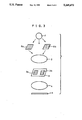
- FIG. 3 shows a schematic diagram of the polarizing exposure apparatus using a polarizer according to the present invention.
- the polarizing exposure apparatus using a polarizer of the present invention comprises a light source 1 for radiating light, a pair of polarizing plates 6a and 6b for respectively polarizing the light radiated from said light source 1, a focusing lens 2 for focusing the light polarized through polarizing plates 6a and 6b, a polarizing mask 3, having patterns 3a and 3b, for passing only light of the desired pattern among from the polarized light focused through focusing lens 2 and a reduction projection lens 4 for forming the desired pattern on wafer 5 by reducing the light passed through polarizing mask 3.
- a pair of polarizing plates 6a and 6b for differently polarizing light from light source 1 are established between light source 1 and focusing lens 2, and polarizing mask 3 for passing only light of the desired pattern from the light focused through focusing lens 2 is established between focusing lens 2 and reduction projection lens 4.
- the light radiated from light source 1 is polarized through either one of polarizing plates 6a and 6b. If the light passes through polarizing plate 6a, the light is polarized through polarizing plate 6a. This polarized light is focused through focusing lens 2 and radiated on to polarizing mask 3.
- FIG. 4 shows a process for fabricating a polarizing mask by using the polarizing exposure apparatus of FIG. 3.
- a Cr layer is deposited on quartz substrate 7 and is patterned to form Cr mask 3c.
- a first polarizing film 8 is formed on the whole surface.
- a photosensitive film 9 is coated on the whole surface and is etched by using photoetching method. Then, first polarizing film 8 is etched so as to remain over Cr mask 3c in a pattern corresponding to patterned photosensitive film 9.
- said photosensitive film 9 is then removed and second polarizing film 10 is formed on the whole surface.
- second polarizing plate 10 is etched by a photoetching method so as to remain over Cr mask 3c in a pattern corresponding to the spaces between the pattern formed by said first polarizing plates 8.
- FIG. 5 shows a graph illustrating the density of the light between the polarizing mask of the present invention and the Cr mask of the prior art.
- the difference of the density of the light is smaller, as indicated at A of FIG. 5. Therefore, it is very difficult to form the desired pattern by using a Cr mask.
- the present invention's polarizing mask case because the difference of the density of the light becomes larger than that of the Cr mask case, as indicated at C of FIG. 5, the resolution can be improved.
- the present invention can improve resolution by using the simple polarizing exposure apparatus described above and it can fabricate the mask by the conventional CAD.
Abstract
Description
Claims (3)
Applications Claiming Priority (2)
| Application Number | Priority Date | Filing Date | Title |
|---|---|---|---|
| KR1019910009736A KR950002172B1 (en) | 1991-06-13 | 1991-06-13 | Polarized light exposuring apparatus and mask manufacturing method using polarizer |
| KR9736/1991 | 1991-06-13 |
Publications (1)
| Publication Number | Publication Date |
|---|---|
| US5245470A true US5245470A (en) | 1993-09-14 |
Family
ID=19315726
Family Applications (1)
| Application Number | Title | Priority Date | Filing Date |
|---|---|---|---|
| US07/844,133 Expired - Lifetime US5245470A (en) | 1991-06-13 | 1992-03-02 | Polarizing exposure apparatus using a polarizer and method for fabrication of a polarizing mask by using a polarizing exposure apparatus |
Country Status (4)
| Country | Link |
|---|---|
| US (1) | US5245470A (en) |
| JP (1) | JP2879634B2 (en) |
| KR (1) | KR950002172B1 (en) |
| DE (1) | DE4211242C2 (en) |
Cited By (22)
| Publication number | Priority date | Publication date | Assignee | Title |
|---|---|---|---|---|
| US5365371A (en) * | 1992-02-10 | 1994-11-15 | Mitsubishi Denki Kabushiki Kaisha | Projection exposure apparatus |
| US5459000A (en) * | 1992-10-14 | 1995-10-17 | Canon Kabushiki Kaisha | Image projection method and device manufacturing method using the image projection method |
| US5677755A (en) * | 1993-10-29 | 1997-10-14 | Hitachi, Ltd. | Method and apparatus for pattern exposure, mask used therefor, and semiconductor integrated circuit produced by using them |
| US5739898A (en) * | 1993-02-03 | 1998-04-14 | Nikon Corporation | Exposure method and apparatus |
| US5933219A (en) * | 1994-04-22 | 1999-08-03 | Canon Kabushiki Kaisha | Projection exposure apparatus and device manufacturing method capable of controlling polarization direction |
| US6145984A (en) * | 1997-12-23 | 2000-11-14 | Maui Jim, Inc. | Color-enhancing polarized lens |
| US20010019404A1 (en) * | 2000-03-03 | 2001-09-06 | Karl-Heinz Schuster | Projection exposure system for microlithography and method for generating microlithographic images |
| US6334680B1 (en) | 1998-02-23 | 2002-01-01 | Optimieyes Limited Partnership | Polarized lens with oxide additive |
| US6604824B2 (en) | 1998-02-23 | 2003-08-12 | Charles P. Larson | Polarized lens with oxide additive |
| US6645678B2 (en) | 2000-12-01 | 2003-11-11 | Motorola, Inc. | Method and apparatus for making an integrated circuit using polarization properties of light |
| US20040010385A1 (en) * | 2002-07-11 | 2004-01-15 | Kabushiki Kaisha Toshiba | Inspection method and a photomask |
| US20040057036A1 (en) * | 2002-09-19 | 2004-03-25 | Miyoko Kawashima | Exposure method |
| US20040263816A1 (en) * | 2003-05-12 | 2004-12-30 | Asml Netherlands B.V. | Lithographic apparatus and device manufacturing method |
| US20050105180A1 (en) * | 2003-11-18 | 2005-05-19 | Jeff Mackey | Polarized reticle, photolithography system, and method of forming a pattern using a polarized reticle in conjunction with polarized light |
| EP1720061A2 (en) * | 2003-01-14 | 2006-11-08 | ASML Netherlands B.V. | Embedded etch stop for phase shift masks and planar phase shift masks to reduce topography induced and wave guide effects |
| US20060286460A1 (en) * | 2005-06-15 | 2006-12-21 | Samsung Electronics Co., Ltd. | Photomask, method of making a photomask and photolithography method and system using the same |
| US20080049208A1 (en) * | 2006-07-13 | 2008-02-28 | Samsung Electronics Co., Ltd | Method of exposing substrate and apparatus for performing the same |
| US20090233191A1 (en) * | 2005-09-01 | 2009-09-17 | Sajan Marokkey | Overlay Target for Polarized Light Lithography |
| US8476004B2 (en) | 2011-06-27 | 2013-07-02 | United Microelectronics Corp. | Method for forming photoresist patterns |
| US8627242B1 (en) | 2013-01-30 | 2014-01-07 | United Microelectronics Corp. | Method for making photomask layout |
| US8701052B1 (en) | 2013-01-23 | 2014-04-15 | United Microelectronics Corp. | Method of optical proximity correction in combination with double patterning technique |
| US9230812B2 (en) | 2013-05-22 | 2016-01-05 | United Microelectronics Corp. | Method for forming semiconductor structure having opening |
Families Citing this family (5)
| Publication number | Priority date | Publication date | Assignee | Title |
|---|---|---|---|---|
| US4899554A (en) * | 1987-01-08 | 1990-02-13 | Sanden Corporation | Refrigerator with plural storage chambers |
| DE10330421A1 (en) * | 2003-07-04 | 2005-02-03 | Leonhard Kurz Gmbh & Co. Kg | Exposure station for film webs |
| JPWO2008001593A1 (en) * | 2006-06-30 | 2009-11-26 | 株式会社ニコン | Exposure method, exposure apparatus, and device manufacturing method |
| CN105974653B (en) * | 2016-07-21 | 2019-05-07 | 京东方科技集团股份有限公司 | Color membrane substrates and its manufacturing method, mask plate and its manufacturing method, display device |
| CN112286005B (en) * | 2020-09-23 | 2022-11-22 | 山东师范大学 | Method for improving resolution of chip photoetching process |
Citations (5)
| Publication number | Priority date | Publication date | Assignee | Title |
|---|---|---|---|---|
| US2316643A (en) * | 1941-06-06 | 1943-04-13 | Eastman Kodak Co | Photomechanical process |
| US2440102A (en) * | 1944-05-31 | 1948-04-20 | Polaroid Corp | Process of manufacture of light polarizing two tone image on a sheet |
| US4937459A (en) * | 1984-11-16 | 1990-06-26 | Canon Kabushiki Kaisha | Alignment signal detecting device |
| US5070250A (en) * | 1989-02-28 | 1991-12-03 | Nikon Corporation | Position detection apparatus with adjustable beam and interference fringe positions |
| US5072126A (en) * | 1990-10-31 | 1991-12-10 | International Business Machines Corporation | Promixity alignment using polarized illumination and double conjugate projection lens |
Family Cites Families (4)
| Publication number | Priority date | Publication date | Assignee | Title |
|---|---|---|---|---|
| DE1572195A1 (en) * | 1965-06-05 | 1970-03-26 | Telefunken Patent | Process for the production of microstructures with a small line width |
| DE3147644A1 (en) * | 1980-12-18 | 1982-11-18 | Balzers Hochvakuum Gmbh, 6200 Wiesbaden | "USE OF A CHROME, IRON AND OXYGEN LAYER FOR THE PRODUCTION OF PHOTO MASKS" |
| FR2536872A1 (en) * | 1982-11-29 | 1984-06-01 | Cii Honeywell Bull | PATTERN GENERATOR FOR INTEGRATED CIRCUITS AND PATTERN GENERATING METHOD USING THE GENERATOR |
| JPH04362949A (en) * | 1991-03-29 | 1992-12-15 | Toshiba Corp | Mask substrate for exposure, projection aligner, and pattern forming method |
-
1991
- 1991-06-13 KR KR1019910009736A patent/KR950002172B1/en not_active IP Right Cessation
-
1992
- 1992-03-02 US US07/844,133 patent/US5245470A/en not_active Expired - Lifetime
- 1992-04-03 DE DE4211242A patent/DE4211242C2/en not_active Expired - Fee Related
- 1992-04-13 JP JP11856692A patent/JP2879634B2/en not_active Expired - Fee Related
Patent Citations (5)
| Publication number | Priority date | Publication date | Assignee | Title |
|---|---|---|---|---|
| US2316643A (en) * | 1941-06-06 | 1943-04-13 | Eastman Kodak Co | Photomechanical process |
| US2440102A (en) * | 1944-05-31 | 1948-04-20 | Polaroid Corp | Process of manufacture of light polarizing two tone image on a sheet |
| US4937459A (en) * | 1984-11-16 | 1990-06-26 | Canon Kabushiki Kaisha | Alignment signal detecting device |
| US5070250A (en) * | 1989-02-28 | 1991-12-03 | Nikon Corporation | Position detection apparatus with adjustable beam and interference fringe positions |
| US5072126A (en) * | 1990-10-31 | 1991-12-10 | International Business Machines Corporation | Promixity alignment using polarized illumination and double conjugate projection lens |
Cited By (48)
| Publication number | Priority date | Publication date | Assignee | Title |
|---|---|---|---|---|
| US5436761A (en) * | 1992-02-10 | 1995-07-25 | Mitsubishi Denki Kabushiki Kaisha | Projection exposure apparatus and polarizer |
| US5365371A (en) * | 1992-02-10 | 1994-11-15 | Mitsubishi Denki Kabushiki Kaisha | Projection exposure apparatus |
| US5459000A (en) * | 1992-10-14 | 1995-10-17 | Canon Kabushiki Kaisha | Image projection method and device manufacturing method using the image projection method |
| US5739898A (en) * | 1993-02-03 | 1998-04-14 | Nikon Corporation | Exposure method and apparatus |
| US5677755A (en) * | 1993-10-29 | 1997-10-14 | Hitachi, Ltd. | Method and apparatus for pattern exposure, mask used therefor, and semiconductor integrated circuit produced by using them |
| US5933219A (en) * | 1994-04-22 | 1999-08-03 | Canon Kabushiki Kaisha | Projection exposure apparatus and device manufacturing method capable of controlling polarization direction |
| US6145984A (en) * | 1997-12-23 | 2000-11-14 | Maui Jim, Inc. | Color-enhancing polarized lens |
| US6604824B2 (en) | 1998-02-23 | 2003-08-12 | Charles P. Larson | Polarized lens with oxide additive |
| US6334680B1 (en) | 1998-02-23 | 2002-01-01 | Optimieyes Limited Partnership | Polarized lens with oxide additive |
| US20050083506A1 (en) * | 2000-03-03 | 2005-04-21 | Carl-Zeiss-Stiftung | Projection exposure system for microlithography and method for generating microlithographic images |
| US6930758B2 (en) * | 2000-03-03 | 2005-08-16 | Carl Zeiss Smt Ag | Projection exposure system for microlithography and method for generating microlithographic images |
| US6972831B2 (en) | 2000-03-03 | 2005-12-06 | Carl-Zeiss-Stiftung | Projection exposure system for microlithography and method for generating microlithographic images |
| US6950174B2 (en) | 2000-03-03 | 2005-09-27 | Carl-Zeiss-Stiftung | Projection exposure system for microlithography and method for generating microlithographic images |
| US20050083507A1 (en) * | 2000-03-03 | 2005-04-21 | Carl-Zeiss-Stiftung | Projection exposure system for microlithography and method for generating microlithographic images |
| US20060023193A1 (en) * | 2000-03-03 | 2006-02-02 | Karl-Heinz Schuster | Projection exposure system for microlithography and method for generating microlithographic images |
| US20010019404A1 (en) * | 2000-03-03 | 2001-09-06 | Karl-Heinz Schuster | Projection exposure system for microlithography and method for generating microlithographic images |
| US7113260B2 (en) | 2000-03-03 | 2006-09-26 | Carl Zeiss Smt Ag | Projection exposure system for microlithography and method for generating microlithographic images |
| US6645678B2 (en) | 2000-12-01 | 2003-11-11 | Motorola, Inc. | Method and apparatus for making an integrated circuit using polarization properties of light |
| US20070071306A1 (en) * | 2002-07-11 | 2007-03-29 | Kabushiki Kaisha Toshiba | Inspection method and photomask |
| US7186485B2 (en) | 2002-07-11 | 2007-03-06 | Kabushiki Kaisha Toshiba | Inspection method and a photomask |
| US7556896B2 (en) | 2002-07-11 | 2009-07-07 | Kabushiki Kaisha Toshiba | Inspection method and photomask |
| US20040010385A1 (en) * | 2002-07-11 | 2004-01-15 | Kabushiki Kaisha Toshiba | Inspection method and a photomask |
| NL1023892C2 (en) * | 2002-07-11 | 2005-12-20 | Toshiba Kk | Inspection method and a photo mask. |
| US7009686B2 (en) * | 2002-09-19 | 2006-03-07 | Canon Kabushiki Kaisha | Exposure method |
| US20040057036A1 (en) * | 2002-09-19 | 2004-03-25 | Miyoko Kawashima | Exposure method |
| EP1720061A2 (en) * | 2003-01-14 | 2006-11-08 | ASML Netherlands B.V. | Embedded etch stop for phase shift masks and planar phase shift masks to reduce topography induced and wave guide effects |
| EP1720061A3 (en) * | 2003-01-14 | 2007-06-20 | ASML Netherlands B.V. | Embedded etch stop for phase shift masks and planar phase shift masks to reduce topography induced and wave guide effects |
| US20040263816A1 (en) * | 2003-05-12 | 2004-12-30 | Asml Netherlands B.V. | Lithographic apparatus and device manufacturing method |
| US7569311B2 (en) | 2003-11-18 | 2009-08-04 | Micron Technology, Inc. | Method of forming a pattern using a polarized reticle in conjunction with polarized light |
| US7592107B2 (en) | 2003-11-18 | 2009-09-22 | Micron Technology, Inc. | Polarized reticle, photolithography system, and method of fabricating a polarized reticle |
| US20050105180A1 (en) * | 2003-11-18 | 2005-05-19 | Jeff Mackey | Polarized reticle, photolithography system, and method of forming a pattern using a polarized reticle in conjunction with polarized light |
| US20070122720A1 (en) * | 2003-11-18 | 2007-05-31 | Jeff Mackey | Polarized reticle, photolithography system, and method of fabricating a polarized reticle |
| US7150945B2 (en) | 2003-11-18 | 2006-12-19 | Micron Technology, Inc. | Polarized reticle, photolithography system, and method of forming a pattern using a polarized reticle in conjunction with polarized light |
| WO2005050317A2 (en) * | 2003-11-18 | 2005-06-02 | Micron Technology, Inc. | Polarized reticle, photolithography system, and method of forming a pattern using a polarized reticle in conjunction with polarized light |
| WO2005050317A3 (en) * | 2003-11-18 | 2005-09-22 | Micron Technology Inc | Polarized reticle, photolithography system, and method of forming a pattern using a polarized reticle in conjunction with polarized light |
| US20070020535A1 (en) * | 2003-11-18 | 2007-01-25 | Jeff Mackey | Method of forming a pattern using a polarized reticle in conjuction with polarized light |
| US20060286460A1 (en) * | 2005-06-15 | 2006-12-21 | Samsung Electronics Co., Ltd. | Photomask, method of making a photomask and photolithography method and system using the same |
| US7629087B2 (en) | 2005-06-15 | 2009-12-08 | Samsung Electronics Co., Ltd. | Photomask, method of making a photomask and photolithography method and system using the same |
| US20090233191A1 (en) * | 2005-09-01 | 2009-09-17 | Sajan Marokkey | Overlay Target for Polarized Light Lithography |
| US7807320B2 (en) | 2005-09-01 | 2010-10-05 | Infineon Technologies Ag | Overlay target for polarized light lithography |
| US20100330469A1 (en) * | 2005-09-01 | 2010-12-30 | Sajan Marokkey | Overlay Target for Polarized Light Lithography |
| US8203223B2 (en) | 2005-09-01 | 2012-06-19 | Infineon Technologies Ag | Overlay target for polarized light lithography |
| US20080049208A1 (en) * | 2006-07-13 | 2008-02-28 | Samsung Electronics Co., Ltd | Method of exposing substrate and apparatus for performing the same |
| US7830496B2 (en) * | 2006-07-13 | 2010-11-09 | Samsung Electronics Co., Ltd. | Method of exposing substrate with one polarization mask and at least two lights and apparatus for performing the same |
| US8476004B2 (en) | 2011-06-27 | 2013-07-02 | United Microelectronics Corp. | Method for forming photoresist patterns |
| US8701052B1 (en) | 2013-01-23 | 2014-04-15 | United Microelectronics Corp. | Method of optical proximity correction in combination with double patterning technique |
| US8627242B1 (en) | 2013-01-30 | 2014-01-07 | United Microelectronics Corp. | Method for making photomask layout |
| US9230812B2 (en) | 2013-05-22 | 2016-01-05 | United Microelectronics Corp. | Method for forming semiconductor structure having opening |
Also Published As
| Publication number | Publication date |
|---|---|
| KR950002172B1 (en) | 1995-03-14 |
| JP2879634B2 (en) | 1999-04-05 |
| JPH05188576A (en) | 1993-07-30 |
| DE4211242A1 (en) | 1992-12-17 |
| KR930001310A (en) | 1993-01-16 |
| DE4211242C2 (en) | 1997-04-24 |
Similar Documents
| Publication | Publication Date | Title |
|---|---|---|
| US5245470A (en) | Polarizing exposure apparatus using a polarizer and method for fabrication of a polarizing mask by using a polarizing exposure apparatus | |
| US5480047A (en) | Method for forming a fine resist pattern | |
| US5935736A (en) | Mask and method to eliminate side-lobe effects in attenuated phase shifting masks | |
| US5902493A (en) | Method for forming micro patterns of semiconductor devices | |
| JPH0690506B2 (en) | Photo mask | |
| JP4613364B2 (en) | Resist pattern formation method | |
| US5300378A (en) | Method of producing a phase shifting mask | |
| JP3164779B2 (en) | Photo mask | |
| JPH10254122A (en) | Photomask for exposure | |
| KR960015792B1 (en) | Mask forming method for pattern of semiconductor device | |
| JP3130777B2 (en) | Photomask and method of manufacturing the same | |
| JP2624351B2 (en) | Photomask manufacturing method | |
| JP3110855B2 (en) | Method of manufacturing projection exposure substrate and pattern forming method using this substrate | |
| JP3475309B2 (en) | Method for manufacturing phase shift photomask | |
| US5576122A (en) | Phase shift mask and manufacturing method thereof | |
| JPH0529197A (en) | Method of forming resist pattern | |
| JP2589060B2 (en) | Reduction projection exposure method | |
| JPH09138497A (en) | Resist exposure method and exposure mask | |
| JP2000082650A (en) | Projection exposure method | |
| JPH04216553A (en) | Mask for production of semiconductor | |
| KR0165402B1 (en) | Phase shift mask and its manufacturing method | |
| JP3031728B2 (en) | Reticle and exposure equipment | |
| JPH03172848A (en) | Manufacture of photomask | |
| JPH06289593A (en) | Production of mask | |
| JPH05333524A (en) | Phase shift mask and its production |
Legal Events
| Date | Code | Title | Description |
|---|---|---|---|
| AS | Assignment |
Owner name: GOLD STAR ELECTRON CO., LTD., KOREA, REPUBLIC OF Free format text: ASSIGNMENT OF ASSIGNORS INTEREST.;ASSIGNOR:KEUM, EUN S.;REEL/FRAME:006033/0710 Effective date: 19920220 |
|
| STCF | Information on status: patent grant |
Free format text: PATENTED CASE |
|
| FEPP | Fee payment procedure |
Free format text: PAYOR NUMBER ASSIGNED (ORIGINAL EVENT CODE: ASPN); ENTITY STATUS OF PATENT OWNER: LARGE ENTITY |
|
| AS | Assignment |
Owner name: LG SEMICON CO., LTD., KOREA, REPUBLIC OF Free format text: CHANGE OF NAME;ASSIGNOR:GOLDSTAR ELECTRON CO., LTD.;REEL/FRAME:007658/0783 Effective date: 19960208 |
|
| FPAY | Fee payment |
Year of fee payment: 4 |
|
| FPAY | Fee payment |
Year of fee payment: 8 |
|
| FPAY | Fee payment |
Year of fee payment: 12 |