US5253157A - Half-bridge inverter with capacitive voltage equalizer - Google Patents
Half-bridge inverter with capacitive voltage equalizer Download PDFInfo
- Publication number
- US5253157A US5253157A US07/831,918 US83191892A US5253157A US 5253157 A US5253157 A US 5253157A US 83191892 A US83191892 A US 83191892A US 5253157 A US5253157 A US 5253157A
- Authority
- US
- United States
- Prior art keywords
- voltage
- capacitor
- inverter circuit
- bridge inverter
- circuit according
- Prior art date
- Legal status (The legal status is an assumption and is not a legal conclusion. Google has not performed a legal analysis and makes no representation as to the accuracy of the status listed.)
- Expired - Fee Related
Links
Images


Classifications
-
- H—ELECTRICITY
- H02—GENERATION; CONVERSION OR DISTRIBUTION OF ELECTRIC POWER
- H02M—APPARATUS FOR CONVERSION BETWEEN AC AND AC, BETWEEN AC AND DC, OR BETWEEN DC AND DC, AND FOR USE WITH MAINS OR SIMILAR POWER SUPPLY SYSTEMS; CONVERSION OF DC OR AC INPUT POWER INTO SURGE OUTPUT POWER; CONTROL OR REGULATION THEREOF
- H02M7/00—Conversion of ac power input into dc power output; Conversion of dc power input into ac power output
- H02M7/42—Conversion of dc power input into ac power output without possibility of reversal
- H02M7/44—Conversion of dc power input into ac power output without possibility of reversal by static converters
- H02M7/48—Conversion of dc power input into ac power output without possibility of reversal by static converters using discharge tubes with control electrode or semiconductor devices with control electrode
- H02M7/53—Conversion of dc power input into ac power output without possibility of reversal by static converters using discharge tubes with control electrode or semiconductor devices with control electrode using devices of a triode or transistor type requiring continuous application of a control signal
- H02M7/537—Conversion of dc power input into ac power output without possibility of reversal by static converters using discharge tubes with control electrode or semiconductor devices with control electrode using devices of a triode or transistor type requiring continuous application of a control signal using semiconductor devices only, e.g. single switched pulse inverters
- H02M7/538—Conversion of dc power input into ac power output without possibility of reversal by static converters using discharge tubes with control electrode or semiconductor devices with control electrode using devices of a triode or transistor type requiring continuous application of a control signal using semiconductor devices only, e.g. single switched pulse inverters in a push-pull configuration
-
- H—ELECTRICITY
- H02—GENERATION; CONVERSION OR DISTRIBUTION OF ELECTRIC POWER
- H02J—CIRCUIT ARRANGEMENTS OR SYSTEMS FOR SUPPLYING OR DISTRIBUTING ELECTRIC POWER; SYSTEMS FOR STORING ELECTRIC ENERGY
- H02J9/00—Circuit arrangements for emergency or stand-by power supply, e.g. for emergency lighting
- H02J9/04—Circuit arrangements for emergency or stand-by power supply, e.g. for emergency lighting in which the distribution system is disconnected from the normal source and connected to a standby source
- H02J9/06—Circuit arrangements for emergency or stand-by power supply, e.g. for emergency lighting in which the distribution system is disconnected from the normal source and connected to a standby source with automatic change-over, e.g. UPS systems
- H02J9/062—Circuit arrangements for emergency or stand-by power supply, e.g. for emergency lighting in which the distribution system is disconnected from the normal source and connected to a standby source with automatic change-over, e.g. UPS systems for AC powered loads
Definitions
- This invention relates generally to the field of electronic power conversion and, in particular, to uninterruptible power supplies (UPS).
- the invention uses low cost circuit topology in order to implement half-bridge inverters which are used in conjunction with a single source of reserve energy storage and an electric storage battery.
- both capacitors will be discharged unequally by the non-symmetrical load but will be charged equally by identical current flow from a charger. This condition will lead to a total discharge of one capacitor which will render the inverter inoperable for its intended purpose due to its inability to produce a symmetrical AC voltage waveform.
- the purpose of this invention is to overcome problems of the prior art associated with non-symmetrical loads as well as to eliminate DC leakage equalization resistors commonly used with capacitors connected in series.
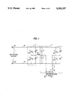
- FIG. 1 is a block diagram of the power circuit of a half-bridge inverter with a capacitive voltage equalizer in accordance with the present invention.
- FIG. 2 is a block diagram of the control circuit of a half-bridge inverter with capacitive voltage equalizer in accordance with the present invention.
- FIG. 3a-c is a diagram showing the current flow in a UPS with a with non-symmetrical load.
- FIG. 4a-f is a timing diagram showing the current waveforms in a UPS with a non-symmetrical load.
- inverter circuit 1 an equalizer circuit 2, input DC source terminals 31 and 32 and output AC terminals 33 and 34.
- inverter circuit 1 there are three parallel circuits connected to buss conductors 35 and 36.
- Conductor 35 is connected to DC source terminal 31 to form a positive buss and conductor 36 is conducted to DC source terminal 32 to form a negative buss.
- the first parallel circuit is formed of capacitors 10 and 11 connected in series with each other.
- the second parallel circuit is formed of power semiconductor switches 12 and 13 connected in series with each other. Switches 12 and 13 have respective control terminals 12A and 13A. The direction of controllable current flow in both semiconductor switches is from positive buss conductor 35 to negative buss conductor 36. The function of control terminals 12A and 13A is to open and close the switches 12 and 13 in accordance with a control voltage.
- semiconductor devices known in the prior art which can be used to perform this function such as bipolar transistors, Darlingtons, MOSFETS, IGBTS, GTOs, etc. Any one of these devices can be used for switches 12 and 13.
- the third parallel circuit is formed of diodes 14 and 15 also connected in series with each other.
- the direction of current flow through both diodes is from negative buss conductor 36 to positive buss conductor 35.
- the center connection of diodes 14 and 15 and the center connection of semiconductor switches 12 and 13 are connected in common via conductor 18 to one side of choke 16 which forms an output filter.
- the other side of choke 16 is connected to filter capacitor 17 and to output load terminal 34.
- the other side of capacitor 17 is connected to a center point of connection between capacitors 10 and 11, and to an output load terminal 33.
- Equalizer 2 is formed of semiconductor switches 21 and 22, diodes 23 and 24, and choke 25.
- Switches 21 and 22 and diodes 23 and 24 are connected together with buss conductors 35 and 36 in a manner similar to switches 12 and 13 and diodes 14 and 15 in inverter 1. Because the current flow through switches 21 and 22 and diodes 23 and 24 is not as great as the current flow through their corresponding parts in inverter 1, their electrical ratings can be lower.
- Choke 25 is connected between the center connection point of switches 21 and 22 and the center connection point of capacitors 10 and 11 in inverter 1.
- the control circuit of the present invention shown in (FIG. 2) is formed of voltage level conditioners 41 and 42.
- the function of these conditioners is to reduce power circuit voltage values and to shift its level if necessary so that common integrated circuits can be used to operate on those voltages.
- Voltage conditioner 41 has its input terminals connected to capacitor 10 via terminals 31 and 33.
- Voltage conditioner 42 has its input terminals connected to capacitor 11 via terminals 32 and 33.
- the transfer characteristics of voltage conditioners 41 and 42 are identical.
- conditioner circuits known in the prior art the simplest of which is a resistive divider.
- the outputs of level conditioners 41 and 42 are supplied to summing amplifier 43.
- the output of a summing amplifier 43 is fed to one input of voltage error amplifier 44.
- the other input of voltage error amplifier 44 is tied to common a voltage reference point which has a zero voltage potential.
- PWM pulse width modulation
- driver 48 The output of PWM circuit 45 is fed to driver 48 and through a logic inverter 46 to a driver 47.
- Both drivers 47 and 48 are identical and their function is to shift the level of the logic voltage in order to make it compatible with the level required by the control terminals of equalizer semiconductor switches 21 and 22 and to provide sufficient power to the control terminals.
- driver circuits well known in the prior art which are based on transformers, optocouplers, and level shifters which can perform the function of drivers 47 and 48.
- driver 47 is supplied to the control terminal of switch 21 and the output of driver 48 is supplied to the control terminal of switch 22.
- An inverter control circuit 50 is connected to input DC source terminals 31 and 32 and to output AC terminals 34 and 33. On the output, circuit 50 is connected to the control terminals of semiconductor switches 12 and 13. There are numerous inverter control circuits known in the prior art which can produce the desired regulated output voltage waveform which may be used to perform the function of control circuit 50.
- inverter circuit 1 When switch 12 is on, the positive voltage on capacitor 10 is applied across the output filter formed of choke coil 16 and capacitor 17. Then current through choke 16 starts increasing. When switch 12 is turned off, the choke current will be switched through diode 15. Inverter 1 is thus operating in a buck converter configuration. At this time, the negative voltage on capacitor 11 is applied to the input of the output filter components and current though choke 16 begins to decrease. If switch 12 is on and off for equal periods of time, the duty cycle is 50% and positive and negative voltage pulses on the input of the output filter are of equal duration but are opposite in polarity. The output filter acts as an averaging filter and therefore the output filter voltage will be zero.
- switch 12 has an on-state duty cycle greater than 50%, a positive voltage will appear on the filter output on load terminals 33 and 34.
- Switch 13 and diode 14 act in the same way as switch 12 and diode 15 but for a current flow through choke 16 in the opposite direction.
- switch 13 has an on-state duty cycle greater than 50%, a negative voltage will appear on the filter output on load terminals 33 and 34.
- Switches 12 and 13 are turned on and off in a complementary fashion, meaning that at any given time one of them is on and the other one is off. This means that the duty cycle of only one switch can be controlled as the other one is a simple logic compliment.
- By varying the duty cycle of the pulse turning a device on it is possible to create an output voltage of any value from a positive value equal to the voltage on capacitor 10 (100% duty cycle for switch 12) to a negative value equal to the voltage on capacitor 11 (100% duty cycle for switch 13).
- control circuit 50 for controlling the operation of switches 12 and 13 produces symmetrical pulse width modulation versus 50% duty cycle, it is important that voltages on capacitors 10 and 11 be equal. Otherwise, the positive and negative halfs of the output AC voltage waveform will be unequal which will have the effect of creating a DC offset voltage on the output. This offset is unacceptable as loads like transformers are in reality short circuits for DC voltage and will cause inverter semiconductor damage or shutdown by control circuits 50.
- Equalizer switches 21 and 22 along with diodes 23 and 24 operate in essentially the same fashion as inverter switches 12 and 13 and diodes 14 and 15. At a 50% duty cycle, the average voltage on the connection point of the equalizer switches will be equal to exactly one half of the DC source voltage.
- the equalizer will then force the voltage at the common connecting point of capacitors 10 and 11 to be exactly one half of DC source voltage. This means that capacitor 10 will have a positive voltage with respect to the neutral output conductor equal to one half of the DC source voltage. Capacitor 11 will have a negative voltage with respect to the same neutral output conductor also equal to one half of the DC source voltage. This will satisfy the inverter control requirements that capacitor voltages be equal but of opposite polarity.
- the timing diagram 4a shows one example of a non-symmetrical load current superimposed over a sine wave load voltage. On the same diagram there is shown a value of the current from the DC voltage source. Its value A equal to RMS value of the load current. Because positive half wave of the load current is substantially larger than negative one in the example shown, value A is much smaller than positive peak current and much larger than negative peak current.
- the equivalent circuit in FIG. 3a depicts the operation for a positive half wave of the load voltage. During this time, the inverter connects the load to capacitor 10. The load current discharges through capacitor 10 and the DC source current charges capacitor 10.
- the timing diagram in FIG. 4b shows the current through capacitor 10 in the absence of an equalizer. Because the DC source charging current is smaller than the load discharge current, the integral of the total current over a cycle of voltage is not zero, rather has a positive discharge characteristic. This means that this capacitor will be discharged to a to zero voltage in the absence of an equalizer.
- the equivalent circuit in FIG. 3b depicts the operation for a negative half wave of the load voltage. During this time, the inverter connects the load to capacitor 11. The load current discharges through capacitor 11 and the DC source current charges capacitor 11.
- the timing diagram in FIG. 4c shows the current through capacitor 11 in the absence of an equalizer. Because the DC source charging current is larger than load discharge current, the integral of the total current over a cycle of voltage is not zero, but rather has a negative charge characteristic. This means that this capacitor will be charged to a full DC source voltage in the absence of an equalizer.
- the effect of the equalizer is to provide an additional constant current source by the presence of choke 25.
- the current in this choke is regulated by the duty cycle of switch 22. This current additionally charges capacitor 10 via diode 23 when switch 22 is off. This current also discharges capacitor 11 via switch 22 when this switch is on.
- the value of this additional current is represented by B as shown on FIG. 4.
- the DC source current represented by value A is offset in such a way that integrals of currents through both capacitors 10 and 11 during one cycle of the output voltage are equal to zero. This means that the voltage on the capacitors is maintained constant.
- FIGS. 4d, 4e, and 4f show the effect of this offsetting current. This offsetting current transfers the charge from capacitor 11 by discharging it via switch 22 to charge capacitor 10 via diode 23.
- FIG. 3c illustrates the operation of the equalizer when the negative half wave of the load current is larger than the positive have wave.
- current flow in choke 25 reverses direction and discharges capacitor 10 via switch 21 and charges capacitor 11 via diode 24.
- control circuit The function of the control circuit is to regulate the duty cycle of switches 21 and 22 in such a way that the voltages on capacitors 10 and 11 are maintained equal. The operation of the system on non-symmetrical loads will thus be sustained.
- level conditioners 41 and 42 translate the voltage on both capacitors to a logic voltage level. The output voltages of those conditioners are of opposite polarity just like voltages on capacitors 10 and 11.
- the outputs of conditioners 41 and 42 are supplied to the inputs of summing amplifier 43.
- the output of amplifier 43 is zero when the capacitor voltages are equal.
- the output of amplifier 43 is connected to one input of error amplifier 44.
- the reference voltage input of this amplifier is connected to a common reference potential of zero volts.
- the output of error amplifier 44 is also zero when the capacitor voltages are the equal.
- the output is connected to the input of PWM circuit 45.
- PWM circuit 45 generate a series of pulses at a frequency much higher than the frequency of the AC output voltage, on the order of 50 times or more.
- the duration of each pulse is 50% of the repetition period when the input voltage is zero. Pulse duration varies in proportion to the input voltage, not necessarily in a linear manner.
- PWM circuit 45 The output of PWM circuit 45 is suppled directly to driver 48 and to driver 47 via logic inverter 46.
- Inverter 46 creates the complementary drive signal required for the operation of switches 21 and 22.
- the driver circuits turn switches 21 and 22 on and off in synchronism with the PWM pulses.
- the duty cycle is 50% which maintains the capacitor voltages at an equal.
- the capacitor voltages become unequal and an error amplifier voltage appears on the input of the PWM circuit, the PWM circuit changes its pulse width in such a way that voltage difference on the capacitors becomes smaller, negative feedback.
- the gain of amplifier 44 determines the difference between the voltage on capacitors 10 and 11 under influence of a non-symmetrical load. This difference can be made as small as desired, e.g., 1% or 0.1%.
- DC source can be a single phase rectifier or converter as well as a battery, alone or in conjunction with a voltage step-up boost converter. As it is clear from description of this invention, there are no adverse effects on inverter operation in the presence of non-symmetrical loads while being powered from a single DC voltage source.
Abstract
Description
Claims (28)
Priority Applications (1)
| Application Number | Priority Date | Filing Date | Title |
|---|---|---|---|
| US07/831,918 US5253157A (en) | 1992-02-06 | 1992-02-06 | Half-bridge inverter with capacitive voltage equalizer |
Applications Claiming Priority (1)
| Application Number | Priority Date | Filing Date | Title |
|---|---|---|---|
| US07/831,918 US5253157A (en) | 1992-02-06 | 1992-02-06 | Half-bridge inverter with capacitive voltage equalizer |
Publications (1)
| Publication Number | Publication Date |
|---|---|
| US5253157A true US5253157A (en) | 1993-10-12 |
Family
ID=25260202
Family Applications (1)
| Application Number | Title | Priority Date | Filing Date |
|---|---|---|---|
| US07/831,918 Expired - Fee Related US5253157A (en) | 1992-02-06 | 1992-02-06 | Half-bridge inverter with capacitive voltage equalizer |
Country Status (1)
| Country | Link |
|---|---|
| US (1) | US5253157A (en) |
Cited By (26)
| Publication number | Priority date | Publication date | Assignee | Title |
|---|---|---|---|---|
| US5375054A (en) * | 1993-02-05 | 1994-12-20 | Abb Management Ag | Converter bridge having two half-bridges connected by bus bars |
| US5381330A (en) * | 1993-09-08 | 1995-01-10 | Grundl & Hoffmann | Half-bridge arrangement for switching electrical power |
| US5434769A (en) * | 1993-10-27 | 1995-07-18 | Premier Power, Inc. | Multi-phase adaptable AC-DC converter |
| US5621634A (en) * | 1995-02-14 | 1997-04-15 | Kabushiki Kaisha Toshiba | Power converter |
| US5657219A (en) * | 1995-08-29 | 1997-08-12 | Crown International, Inc. | Opposed current power converter |
| US5723913A (en) * | 1994-12-06 | 1998-03-03 | Performance Controls, Inc. | High-voltage electronic switching circuit |
| US6038157A (en) * | 1998-05-28 | 2000-03-14 | Inductotherm Corp. | Fault tolerant power supply circuit |
| US6094035A (en) * | 1999-08-20 | 2000-07-25 | Gain Technology Corporation | Amplifying power converter circuits |
| US6144190A (en) * | 1999-03-25 | 2000-11-07 | Coleman Powermate, Inc. | Energy conversion system employing stabilized half-bridge inverter |
| US6185118B1 (en) * | 1999-04-21 | 2001-02-06 | Infineon Technologies Ag | Driver circuit for driving a half bridge |
| EP1076403A2 (en) * | 1999-08-13 | 2001-02-14 | Powerware Corporation | Multi-mode power converters incorporating balancer circuits and methods of operation thereof |
| US6266260B1 (en) | 1999-09-03 | 2001-07-24 | Powerware Corporation | Inverter having center switch and uninterruptible power supply implementing same |
| DE10010278A1 (en) * | 2000-03-02 | 2001-09-06 | Peter Mandl | Circuit arrangement for rectifier with variable output parameters e.g. for starting DC motor, has terminals of AC sources, except the star-point terminals with multiphase systems |
| WO2001065659A2 (en) * | 2000-02-29 | 2001-09-07 | Powerware Corporation | Power converters with ac and dc operating modes and methods of operation thereof |
| US6483730B2 (en) | 1999-08-13 | 2002-11-19 | Powerware Corporation | Power converters with AC and DC operating modes and methods of operation thereof |
| US6819576B2 (en) | 1999-08-13 | 2004-11-16 | Powerware Corporation | Power conversion apparatus and methods using balancer circuits |
| US20050168157A1 (en) * | 2004-01-30 | 2005-08-04 | Janos Melis | Half-bridge inverter for asymmetrical loads |
| US20070216452A1 (en) * | 2006-03-17 | 2007-09-20 | Takaie Matsumoto | Power supply for a vehicle |
| US20090115340A1 (en) * | 2007-11-05 | 2009-05-07 | General Electric Company | Method and system for eliminating dc bias on electrolytic capacitors and shutdown detecting circuit for current fed ballast |
| US20090161392A1 (en) * | 2007-12-19 | 2009-06-25 | Hong Zhang | Dc component elimination at output voltage of pwm inverters |
| CN1929279B (en) * | 2006-08-16 | 2010-05-12 | 南京航空航天大学 | Magnetism-integrated double decompression semi-bridge converter |
| US20110253706A1 (en) * | 2010-04-15 | 2011-10-20 | Delta Electronics, Inc. | Heating device with plural induction coils |
| US20120025609A1 (en) * | 2011-09-22 | 2012-02-02 | Renewable Power Conversion, Inc. | Very high efficiency uninterruptible power supply |
| US10381917B2 (en) * | 2017-03-23 | 2019-08-13 | Eaton Intelligent Power Limited | Power converter apparatus and methods using adaptive node balancing |
| US10439414B2 (en) | 2017-03-23 | 2019-10-08 | Eaton Intelligent Power Limited | Auto adjusting balancer apparatus |
| US10812014B1 (en) * | 2018-04-05 | 2020-10-20 | The Regents Of The University Of Colorado | Modular photovoltaic string inverter system adapted for SiC MOSFETs |
Citations (7)
| Publication number | Priority date | Publication date | Assignee | Title |
|---|---|---|---|---|
| US4158881A (en) * | 1978-06-12 | 1979-06-19 | Litton Systems, Inc. | DC to DC converter |
| US4639849A (en) * | 1985-05-08 | 1987-01-27 | International Exide Electronics/Corporation | Snubber circuit for H.F. bridge converter |
| US4935861A (en) * | 1989-06-13 | 1990-06-19 | Exide Electronics | Uninterrupted power supply having no low frequency power magnetics |
| US4980812A (en) * | 1989-11-09 | 1990-12-25 | Exide Electronics | Uninterrupted power supply system having improved power factor correction circuit |
| US5068573A (en) * | 1990-09-20 | 1991-11-26 | North American Philips Corporation | Power supply with energy storage for improved voltage regulation |
| US5099410A (en) * | 1990-11-13 | 1992-03-24 | Wisconsin Alumni Research Foundation | Single phase ac power conversion apparatus |
| US5119283A (en) * | 1991-06-10 | 1992-06-02 | General Electric Company | High power factor, voltage-doubler rectifier |
-
1992
- 1992-02-06 US US07/831,918 patent/US5253157A/en not_active Expired - Fee Related
Patent Citations (7)
| Publication number | Priority date | Publication date | Assignee | Title |
|---|---|---|---|---|
| US4158881A (en) * | 1978-06-12 | 1979-06-19 | Litton Systems, Inc. | DC to DC converter |
| US4639849A (en) * | 1985-05-08 | 1987-01-27 | International Exide Electronics/Corporation | Snubber circuit for H.F. bridge converter |
| US4935861A (en) * | 1989-06-13 | 1990-06-19 | Exide Electronics | Uninterrupted power supply having no low frequency power magnetics |
| US4980812A (en) * | 1989-11-09 | 1990-12-25 | Exide Electronics | Uninterrupted power supply system having improved power factor correction circuit |
| US5068573A (en) * | 1990-09-20 | 1991-11-26 | North American Philips Corporation | Power supply with energy storage for improved voltage regulation |
| US5099410A (en) * | 1990-11-13 | 1992-03-24 | Wisconsin Alumni Research Foundation | Single phase ac power conversion apparatus |
| US5119283A (en) * | 1991-06-10 | 1992-06-02 | General Electric Company | High power factor, voltage-doubler rectifier |
Cited By (39)
| Publication number | Priority date | Publication date | Assignee | Title |
|---|---|---|---|---|
| US5375054A (en) * | 1993-02-05 | 1994-12-20 | Abb Management Ag | Converter bridge having two half-bridges connected by bus bars |
| US5381330A (en) * | 1993-09-08 | 1995-01-10 | Grundl & Hoffmann | Half-bridge arrangement for switching electrical power |
| US5434769A (en) * | 1993-10-27 | 1995-07-18 | Premier Power, Inc. | Multi-phase adaptable AC-DC converter |
| US5723913A (en) * | 1994-12-06 | 1998-03-03 | Performance Controls, Inc. | High-voltage electronic switching circuit |
| US5621634A (en) * | 1995-02-14 | 1997-04-15 | Kabushiki Kaisha Toshiba | Power converter |
| US5657219A (en) * | 1995-08-29 | 1997-08-12 | Crown International, Inc. | Opposed current power converter |
| AU757390B2 (en) * | 1998-05-28 | 2003-02-20 | Inductotherm Corp. | Fault tolerant power supply circuit |
| US6038157A (en) * | 1998-05-28 | 2000-03-14 | Inductotherm Corp. | Fault tolerant power supply circuit |
| US6144190A (en) * | 1999-03-25 | 2000-11-07 | Coleman Powermate, Inc. | Energy conversion system employing stabilized half-bridge inverter |
| US6185118B1 (en) * | 1999-04-21 | 2001-02-06 | Infineon Technologies Ag | Driver circuit for driving a half bridge |
| AU764387B2 (en) * | 1999-08-13 | 2003-08-14 | Powerware Corporation | Multi-mode power converters incorporating balancer circuits and methods of operation thereof |
| EP1076403A2 (en) * | 1999-08-13 | 2001-02-14 | Powerware Corporation | Multi-mode power converters incorporating balancer circuits and methods of operation thereof |
| US6819576B2 (en) | 1999-08-13 | 2004-11-16 | Powerware Corporation | Power conversion apparatus and methods using balancer circuits |
| EP1076403A3 (en) * | 1999-08-13 | 2002-01-02 | Powerware Corporation | Multi-mode power converters incorporating balancer circuits and methods of operation thereof |
| US6483730B2 (en) | 1999-08-13 | 2002-11-19 | Powerware Corporation | Power converters with AC and DC operating modes and methods of operation thereof |
| US6094035A (en) * | 1999-08-20 | 2000-07-25 | Gain Technology Corporation | Amplifying power converter circuits |
| US6266260B1 (en) | 1999-09-03 | 2001-07-24 | Powerware Corporation | Inverter having center switch and uninterruptible power supply implementing same |
| WO2001065659A3 (en) * | 2000-02-29 | 2002-03-14 | Powerware Corp | Power converters with ac and dc operating modes and methods of operation thereof |
| WO2001065659A2 (en) * | 2000-02-29 | 2001-09-07 | Powerware Corporation | Power converters with ac and dc operating modes and methods of operation thereof |
| DE10010278A1 (en) * | 2000-03-02 | 2001-09-06 | Peter Mandl | Circuit arrangement for rectifier with variable output parameters e.g. for starting DC motor, has terminals of AC sources, except the star-point terminals with multiphase systems |
| US20050168157A1 (en) * | 2004-01-30 | 2005-08-04 | Janos Melis | Half-bridge inverter for asymmetrical loads |
| US6936974B2 (en) | 2004-01-30 | 2005-08-30 | Ballastronic, Inc. | Half-bridge inverter for asymmetrical loads |
| US20070216452A1 (en) * | 2006-03-17 | 2007-09-20 | Takaie Matsumoto | Power supply for a vehicle |
| US7667342B2 (en) * | 2006-03-17 | 2010-02-23 | Yamaha Hatsudoki Kabushiki Kaisha | Power supply for a vehicle |
| CN1929279B (en) * | 2006-08-16 | 2010-05-12 | 南京航空航天大学 | Magnetism-integrated double decompression semi-bridge converter |
| CN101849440A (en) * | 2007-11-05 | 2010-09-29 | 通用电气公司 | Method and system for eliminating DC bias on electrolytic capacitors and shutdown detecting circuit for current fed ballast |
| US20090115340A1 (en) * | 2007-11-05 | 2009-05-07 | General Electric Company | Method and system for eliminating dc bias on electrolytic capacitors and shutdown detecting circuit for current fed ballast |
| WO2009061564A1 (en) * | 2007-11-05 | 2009-05-14 | General Electric Company | Method and system for eliminating dc bias on electrolytic capacitors and shutdown detecting circuit for current fed ballast |
| US7733028B2 (en) | 2007-11-05 | 2010-06-08 | General Electric Company | Method and system for eliminating DC bias on electrolytic capacitors and shutdown detecting circuit for current fed ballast |
| US20090161392A1 (en) * | 2007-12-19 | 2009-06-25 | Hong Zhang | Dc component elimination at output voltage of pwm inverters |
| US7830682B2 (en) * | 2007-12-19 | 2010-11-09 | Honeywell International Inc. | DC component elimination at output voltage of PWM inverters |
| US20110253706A1 (en) * | 2010-04-15 | 2011-10-20 | Delta Electronics, Inc. | Heating device with plural induction coils |
| US20120025609A1 (en) * | 2011-09-22 | 2012-02-02 | Renewable Power Conversion, Inc. | Very high efficiency uninterruptible power supply |
| US9203323B2 (en) * | 2011-09-22 | 2015-12-01 | Renewable Power Conversion, Inc. | Very high efficiency uninterruptible power supply |
| US10381917B2 (en) * | 2017-03-23 | 2019-08-13 | Eaton Intelligent Power Limited | Power converter apparatus and methods using adaptive node balancing |
| US10439414B2 (en) | 2017-03-23 | 2019-10-08 | Eaton Intelligent Power Limited | Auto adjusting balancer apparatus |
| US10855167B2 (en) | 2017-03-23 | 2020-12-01 | Eaton Intelligent Power Limited | Power converter apparatus and methods using adaptive node balancing |
| US10944280B2 (en) | 2017-03-23 | 2021-03-09 | Eaton Intelligent Power Limited | Auto adjusting balancer apparatus |
| US10812014B1 (en) * | 2018-04-05 | 2020-10-20 | The Regents Of The University Of Colorado | Modular photovoltaic string inverter system adapted for SiC MOSFETs |
Similar Documents
| Publication | Publication Date | Title |
|---|---|---|
| US5253157A (en) | Half-bridge inverter with capacitive voltage equalizer | |
| EP0500789B1 (en) | An uninterrupted power supply system having improved power factor correction circuit | |
| US5504418A (en) | Full shunt boost switching voltage limiter for solar panel array | |
| US5440179A (en) | UPS with bi-directional power flow | |
| US5914590A (en) | Electrical power regulator | |
| US5483433A (en) | Voltage control circuit for a multiple stage DC power supply, and applications thereof | |
| US6483730B2 (en) | Power converters with AC and DC operating modes and methods of operation thereof | |
| US6314007B2 (en) | Multi-mode power converters incorporating balancer circuits and methods of operation thereof | |
| JP3634443B2 (en) | Inductive load control circuit | |
| US5519306A (en) | Constant voltage circuit and a stabilized power supply unit | |
| US7599204B2 (en) | Control scheme providing a freewheeling period in a cyclo-converter and a high frequency inverter | |
| EP0291120B1 (en) | A regulated high frequency power supply | |
| US5896280A (en) | Frequency converter and improved UPS employing the same | |
| US4866591A (en) | Regulated transformer rectifier unit | |
| US20040189265A1 (en) | Constant current regulator using IGBT's with simplified timing | |
| US6963497B1 (en) | Power converter with an inductor input and switched capacitor outputs | |
| CN110739848A (en) | High-gain DC-DC converter for electric vehicle | |
| US7688044B2 (en) | Device for transforming and stabilizing a primary AC voltage for supplying an electric load | |
| JP3290746B2 (en) | Low-loss power supply including DC / DC converter | |
| JP7426397B2 (en) | Power electronic devices and methods for supplying voltage to drive circuits of power semiconductor switches | |
| US5434769A (en) | Multi-phase adaptable AC-DC converter | |
| JPH07135769A (en) | Dc resonance converter | |
| EP4254759A1 (en) | Dc/dc converter for battery chargers, and method of controlling such a dc/dc converter at very light load conditions | |
| CN218514276U (en) | Bootstrap capacitor voltage-stabilizing auxiliary circuit and power converter with same | |
| JPH07298513A (en) | Battery charger for electric vehicle |
Legal Events
| Date | Code | Title | Description |
|---|---|---|---|
| AS | Assignment |
Owner name: PREMIER POWER, INC. A VA CORPORATION, VIRGINIA Free format text: ASSIGNMENT OF ASSIGNORS INTEREST.;ASSIGNOR:SEVERINSKY, ALEX J.;REEL/FRAME:006072/0893 Effective date: 19920403 |
|
| AS | Assignment |
Owner name: ELECTRIC POWER CONVERSION, LTD., ANGUILLA Free format text: ASSIGNMENT OF ASSIGNORS INTEREST;ASSIGNOR:PREMIER POWER, INC.;REEL/FRAME:007526/0144 Effective date: 19950602 Owner name: ELECTRIC POWER CONVERSION, LTD., ANGUILLA Free format text: ASSIGNMENT OF ASSIGNORS INTEREST;ASSIGNOR:PREMIER POWER, INC.;REEL/FRAME:007526/0171 Effective date: 19950605 |
|
| FEPP | Fee payment procedure |
Free format text: PAT HOLDER CLAIMS SMALL ENTITY STATUS - SMALL BUSINESS (ORIGINAL EVENT CODE: SM02); ENTITY STATUS OF PATENT OWNER: SMALL ENTITY |
|
| FPAY | Fee payment |
Year of fee payment: 4 |
|
| REMI | Maintenance fee reminder mailed | ||
| LAPS | Lapse for failure to pay maintenance fees | ||
| STCH | Information on status: patent discontinuation |
Free format text: PATENT EXPIRED DUE TO NONPAYMENT OF MAINTENANCE FEES UNDER 37 CFR 1.362 |
|
| FP | Lapsed due to failure to pay maintenance fee |
Effective date: 20011012 |