US5260592A - Integrating photosensor and imaging system having wide dynamic range with varactors - Google Patents
Integrating photosensor and imaging system having wide dynamic range with varactors Download PDFInfo
- Publication number
- US5260592A US5260592A US07/760,569 US76056991A US5260592A US 5260592 A US5260592 A US 5260592A US 76056991 A US76056991 A US 76056991A US 5260592 A US5260592 A US 5260592A
- Authority
- US
- United States
- Prior art keywords
- sense
- integrating
- output
- sense amplifiers
- imaging array
- Prior art date
- Legal status (The legal status is an assumption and is not a legal conclusion. Google has not performed a legal analysis and makes no representation as to the accuracy of the status listed.)
- Expired - Lifetime
Links
- 238000003384 imaging method Methods 0.000 title claims description 41
- 239000003990 capacitor Substances 0.000 claims abstract description 20
- 239000004065 semiconductor Substances 0.000 claims description 11
- 239000000758 substrate Substances 0.000 claims description 9
- 229910021420 polycrystalline silicon Inorganic materials 0.000 claims description 5
- 229920005591 polysilicon Polymers 0.000 claims description 5
- 239000000463 material Substances 0.000 claims 3
- 239000011159 matrix material Substances 0.000 claims 2
- 230000006835 compression Effects 0.000 abstract description 4
- 238000007906 compression Methods 0.000 abstract description 4
- 238000000034 method Methods 0.000 description 12
- 230000008569 process Effects 0.000 description 9
- 238000010586 diagram Methods 0.000 description 7
- 238000005516 engineering process Methods 0.000 description 5
- 239000002184 metal Substances 0.000 description 5
- 238000003491 array Methods 0.000 description 3
- 238000009792 diffusion process Methods 0.000 description 3
- 238000004519 manufacturing process Methods 0.000 description 3
- 230000008878 coupling Effects 0.000 description 2
- 238000010168 coupling process Methods 0.000 description 2
- 238000005859 coupling reaction Methods 0.000 description 2
- 230000007423 decrease Effects 0.000 description 2
- 230000003247 decreasing effect Effects 0.000 description 2
- 239000007943 implant Substances 0.000 description 2
- 230000001537 neural effect Effects 0.000 description 2
- 230000035945 sensitivity Effects 0.000 description 2
- 230000009471 action Effects 0.000 description 1
- 238000013459 approach Methods 0.000 description 1
- 210000003323 beak Anatomy 0.000 description 1
- 230000008901 benefit Effects 0.000 description 1
- 230000015572 biosynthetic process Effects 0.000 description 1
- 239000000969 carrier Substances 0.000 description 1
- 230000015556 catabolic process Effects 0.000 description 1
- 239000002800 charge carrier Substances 0.000 description 1
- 230000002860 competitive effect Effects 0.000 description 1
- 239000004020 conductor Substances 0.000 description 1
- 238000006073 displacement reaction Methods 0.000 description 1
- 239000002019 doping agent Substances 0.000 description 1
- 230000000694 effects Effects 0.000 description 1
- 238000002513 implantation Methods 0.000 description 1
- 210000003127 knee Anatomy 0.000 description 1
- 238000001465 metallisation Methods 0.000 description 1
- 150000004767 nitrides Chemical class 0.000 description 1
- 229910021332 silicide Inorganic materials 0.000 description 1
- FVBUAEGBCNSCDD-UHFFFAOYSA-N silicide(4-) Chemical compound [Si-4] FVBUAEGBCNSCDD-UHFFFAOYSA-N 0.000 description 1
- 239000002699 waste material Substances 0.000 description 1
Images


Classifications
-
- H—ELECTRICITY
- H01—ELECTRIC ELEMENTS
- H01L—SEMICONDUCTOR DEVICES NOT COVERED BY CLASS H10
- H01L27/00—Devices consisting of a plurality of semiconductor or other solid-state components formed in or on a common substrate
- H01L27/14—Devices consisting of a plurality of semiconductor or other solid-state components formed in or on a common substrate including semiconductor components sensitive to infrared radiation, light, electromagnetic radiation of shorter wavelength or corpuscular radiation and specially adapted either for the conversion of the energy of such radiation into electrical energy or for the control of electrical energy by such radiation
- H01L27/144—Devices controlled by radiation
- H01L27/146—Imager structures
- H01L27/14681—Bipolar transistor imagers
Definitions
- the present invention relates to imaging arrays and systems. More particularly, the present invention relates to a single-chip high-sensitivity imaging system for producing serial-scanned outputs.
- Imaging circuits typically include a two-dimensional array of photosensors, each of which converts a pixel of light energy from an image into an electrical signal representing the light value of the pixel.
- the imaging circuit scans the photosensors to read out the electrical signals representing the light values of all pixels from an image.
- CCD charge coupled device
- the transport of charge in a CCD structure can be accomplished with almost perfect efficiency at video rates; typically less than ten parts per million of the charge in a well is lost in each transfer.
- a typical serial-scanned CCD imager such as is used for video applications, the charge is shifted out once per frame, and hence the total charge in each well is collected over the entire frame time, typically 1/60 second.
- Sensing technologies which operate in this manner, by accumulating charge over the entire time between scanout events, are called integrating photosensors.
- CCD technology has its limitations. Because the photo-generated charge is shifted directly, the gain of the device (electrons out per photon in) is always less than unity. Because the charge stored in each well is limited, the CCD imager has severe dynamic-range constraints. At the low end, the sensitivity is limited by how small a charge can be sensed above the noise of the readout amplifier. At the high end, the range is limited by the total charge that can be shifted from one well into the next.
- Phototransistors can have gain of over 100 electrons per absorbed photon.
- the photocurrent from each phototransistor is fed into a device with exponential current-voltage characteristics, such as a pair of diode-connected MOS transistors.
- the output voltage of such a device is then a logarithmic function of the light level.
- Photons absorbed in the neighborhood of a phototransistor collector-base or emitter-base junction create electron-hole pairs that are collected by the nearest p-n junction. Minority carriers collected by either junction act as base current, and are multiplied by the current gain of the transistor to produce the collector current.
- the emitter current is the sum of the base current and the collector current. For this reason, the emitter current is usually used as the output of the sensor.
- Prior art phototransistor sensors suffer from low-current limitations.
- the current-gain of the phototransistor sensor device is high at high photocurrents, where it is not needed, and is low at low photocurrents, where it would desirably be higher. Because of this behavior of phototransistors, they have not found widespread use in commercial scanned imagers.
- a bipolar phototransistor used as a pixel comprises both an integrating photosensor and a select device.
- the base terminal of the bipolar phototransistor is utilized as the select node for the pixel.
- a plurality of integrating photosensors according to the present invention may be placed in an array of rows and columns, wherein the base terminals of all bipolar phototransistors in a row are capacitively coupled to a common row-select line.
- the emitter of the bipolar phototransistor is the output node of the integrating photosensor.
- the output nodes of all integrating photosensors in a column are connected together to a column sense line.
- the integrating photosensor array is coupled to plurality of sense amplifiers, with a sense amplifier input connected to the sense line output of each column of integrating photosensors.
- An integrating sense amplifier according to the present invention includes an amplifying element having an inverting input is connected to the sense line.
- an MOS balance transistor is connected between the inverting input and the output of the amplifying element and a capacitor, preferably a varactor, is also connected between the inverting input and output of the amplifying element.
- an exponential feedback element can be connected between the output and the inverting input of the amplifying element.
- this feedback element includes a first P-channel feedback transistor having its source connected to the sense line and its gate and drain connected together to the source of a second P-channel feedback transistor. The gate of the second P-channel feedback transistor is connected to the output of the amplifying element, and its drain is connected to a fixed voltage source, such as ground.
- this feedback element includes an N-channel MOS transistor having its source connected to the output of the amplifying element, its drain connected to the input of the amplifying element, and its gate connected to a source of fixed voltage.
- FIG. 1 is a graph showing the measured current gain of a typical phototransistor sensor device as a function of its base current.
- FIG. 2a is a schematic diagram of an integrating photosensor according to a presently-preferred embodiment of the invention.
- FIG. 2b is a cross sectional view of an embodiment of the circuit of FIG. 2a implemented in an N-well CMOS process.
- FIG. 3 is a prior art sense amplifier suitable for use in the present invention.
- FIG. 4a is a schematic diagram of a presently-preferred sense for use in the present invention which provides signal compression.
- FIG. 4b is a graph showing the capacitance of the varactor structure of the sense amplifier of FIG. 4a as a function of voltage.
- FIG. 5 is a graph showing the output voltage of the sense amplifier of FIG. 4a as a function of light intensity.
- FIG. 6a is a schematic diagram of an alternative sense amplifier for use in the present invention incorporating a first exponential feedback element.
- FIG. 6b is a schematic diagram of an alternative sense amplifier for use in the present invention incorporating a second exponential feedback element.
- FIG. 7 a is a block diagram of an imaging array comprising bipolar transistor integrating photosensors according to a presently preferred embodiment of the invention.
- FIG. 7b is a block diagram of an imaging array comprising integrating according to a presently preferred embodiment of the invention.
- FIG. 8a is a cross-sectional view of a portion of an array of integrating photosensors according to a presently preferred embodiment of the invention implemented in an N-well CMOS process taken along an axis parallel to one row thereof in a position which bisects a row-select line of the array.
- FIG. 8b is another cross-sectional view of the integrating photosensor array shown in FIG. 8a, taken along an axis parallel to a column thereof in a position which bisects a column sense line of the array.
- FIG. 1 shows the measured current gain of a typical phototransistor sensor device as a function of its base current. It can be seen that the current-gain of the phototransistor photosensor device is high at high photocurrents, where it is not needed, and is low at low photocurrents, where it would desirably be higher. Because of this behavior, phototransistors have not found widespread use in commercial scanned imagers.
- the photosensor circuit 10 comprises NPN phototransistor 12, having its collector connected to a source of positive voltage, shown as V DD in FIG. 2a.
- NPN phototransistor 12 preferably has a current gain larger than 100.
- a capacitor 14 is shown coupling the base of phototransistor 12 to a select line 16.
- Coupled the base of phototransistor 12 to a select line 16 allows the phototransistor to also be used as a select device.
- the emitter of phototransistor is the output of the integrating photosensor and is connected to column sense line 18.
- a plurality of photosensor circuits 10 are formed in an N-well in a standard N-well CMOS integrated circuit fabrication process, with the single addition of a p-type base diffusion step. Because the N-well diffusion covers the entire photosensor array, the individual pixel circuits can be very dense since there are no large well-to-well spacing distances which waste semiconductor substrate area.
- FIG. 2b a cross section of a presently preferred embodiment of a photosensor circuit 10 in an N-well 15 CMOS process is shown.
- the entire array of photosensors 10 may be fabricated in N-well 20 formed in semiconductor substrate 22.
- N-well 20 forms the collector of all phototransistors 12 in the entire photosensor array.
- the p-base regions 24 of the individual phototransistors 12 are formed by implantation into regions of N-well 20 through apertures in a thick oxide layer 26.
- a gate oxide layer 28 forms the dielectric for capacitor 14, whose plates comprise p-type base region 24 and row-select line 16, comprising a polysilicon layer.
- An N+ region 30 in p-type base region 24 forms the emitter of phototransistor 12.
- N+ region 30 is formed by implanting an n-type dopant through an aperture in row-select line 16 and gate oxide layer 28.
- An oxide layer 32 is deposited over row-select line 16, and a metal contact to sense line 18 formed in oxide layer 32, using conventional semiconductor processing techniques.
- the integrating photosensor of the present invention may easily be integrated into a standard CMOS fabrication process.
- the step used to form the p-type base regions 24 is the only additional step necessary and is performed after field oxide formation and nitride strip or similar step.
- the gate oxide layer 28 and row select line 16 are formed during the steps which form the gate oxide and polysilicon gates of the MOS devices.
- the emitter 30 is formed during the n+ source/drain implant step and the sense line 18 is formed during the contact and metallization steps. All of these steps are already present in a standard CMOS fabrication process.
- NPN phototransistor 12 may have a base region about 7 microns by 7 microns.
- the entire pixel may be 10 microns by 10 microns or less, allowing for a highly dense array and making it competitive with the high quality CCD imager circuits.
- row-select line 16 is held at a fixed voltage selected to reverse bias the base-emitter junction of phototransistor 12. Under this condition, the photocurrent integrates on capacitor 14. When it is desired to read out the state of a selected pixel, row-select line 16 is brought high, thereby forward biasing the base-emitter junction of phototransistor 12. Under this condition, the integrated photocurrent, multiplied by the current gain of phototransistor 12, flows from the emitter of phototransistor 12 onto column sense line 18.
- phototransistor 12 is operated at much higher currents than the photocurrent. At this higher current level, the current gain of phototransistor 12 is much higher than unity as shown in FIG. 1.
- the mode of operation contemplated by the present invention thereby allows many charge carriers to be delivered to sense line 20 for every photo-generated carrier collected by the base.
- Sense amplifier 50 includes an amplifying element 52, which may be an operational amplifier.
- the non-inverting input of amplifier 52 is connected to a source of reference voltage V ref and its inverting input is connected to sense line 18.
- a P-channel balance transistor 54 is connected between the inverting input and the output of amplifier 52. Its gate is connected to a balance line 56.
- a capacitor 58 is also connected between the inverting input and output of amplifier 52.
- amplifier 52 Before row select line 16 is brought high to read a pixel value, amplifier 52 is brought into a known state by bringing the gate of p-channel balance transistor 56 low to turn it on, thereby effectively shorting the inverting input of amplifier 52 to its output and hence driving both input and output voltages to reference voltage V ref .
- the gate of P-channel balance transistor 56 is then brought high, thereby isolating the input sense line 20 from the output of amplifier 52.
- the pixel is then addressed by bringing its row select line high, thus delivering its stored charge multiplied by the current gain of its phototransistor onto sense line 18.
- Amplifier 52 will respond to this charge by maintaining its input at a nearly constant level by the feedback action of capacitor 58.
- the output voltage of amplifier 52 after the pixel has delivered all of its charge to sense line 50 will be lower than its initial value by that charge divided by the value of capacitor 58.
- Sense amplifier 60 includes most of the elements of sense amplifier 50. These elements have been assigned the same reference numerals as the corresponding elements of FIG. 3. Thus, sense amplifier 60 includes an amplifying element 52, having its non-inverting input connected to a source of reference voltage V ref and its inverting input connected to sense line 18. P-channel balance transistor 54 is connected between the inverting input and the output of amplifier 52. Its gate is connected to a balance line 56.
- a varactor structure is connected between the inverting input and output of amplifier 52 in the sense amplifier of FIG. 4a.
- a varactor structure may comprise a large-area MOS transistor.
- the gate of the MOS transistor comprises one terminal of the varactor structure and the other terminal of the varactor structure comprises the source and drain of the MOS transistor connected together.
- Either an N-channel MOS transistor or a P-channel MOS transistor may be used as the varactor according to the present invention. Because, in the presently illustrated application, a positive charge is to be sensed, if an N-channel MOS transistor is used as the varactor as indicated at reference numeral 62, its gate is connected to the input of amplifying element 52 and its source and drain are connected to the output of amplifying element 52. If a P-channel MOS transistor is used as the varactor as indicated at reference numeral 64 in phantom connection, its source and drain are connected to the input of amplifying element 52 and its gate is connected to the output of amplifying element 52. If a charge of the opposite sign is to be sensed, those of ordinary skill in the art will realize that the connections to the varactor will be reversed. If an application requires sensing charge of both polarities, two varactors connected in opposite directions may be used.
- FIG. 4b a graph of varactor gate-to-source capacitance as a function of V GS , the voltage across the capacitor, it may be seen that the capacitance from one terminal of the varactor structure to its other terminal varies with the voltage across the varactor device.
- the capacitance C 0 is small and is determined by the overlap of the gate with the source and drain diffusions.
- V t of the MOS transistor As the gate voltage approaches the threshold voltage V t of the MOS transistor, a channel begins to form under the gate, and the capacitance increases exponentially. Above the threshold voltage, the capacitance reaches the maximum value C ox set by the oxide capacitance of the entire area of the MOS transistor.
- the varactor is oriented in sense amplifier 60 such that the capacitance increases as the input charge increases. For this reason, the output voltage of the sense amplifier 60 per unit photosensor charge is a decreasing function of the total charge sensed. For example, for the NPN phototransistor 12 of FIG. 2a, a positive charge is sensed at the input of sense amplifier 60, causing the amplifier output to go negative from its balanced value. As the source of N-channel varactor 62 is made more negative than the gate, a channel is formed and the gate-to-source capacitance increases.
- FIG. 5 a typical graph of the output voltage of the sense amplifier 60 of FIG. 4a is shown as a function of light intensity.
- the voltage (Y) axis is calibrated in volts and the light-intensity (X) axis is calibrated approximately in mW/meter 2 .
- the region past the knee of the curve in the graph of FIG. 5 represents the region where the capacitance of the varactor is increasing towards the value of C ox . Varying the size of the varactor device will translate the curve along the X-axis. Reducing the minimum capacitance C 0 will translate the lower portion of the curve to the left.
- the horizontal displacement between the upper and lower portions of the curve of FIG. 5 is equal to the ratio of C ox to C 0 .
- Sense amplifier 70 includes all of the elements of sense amplifier 60. These elements have been assigned the same reference numerals as the corresponding elements of FIG. 4a.
- sense amplifier 70 in addition to the elements of the sense amplifier circuit 60 of FIG. 4a, sense amplifier 70 includes an exponential feedback element 72.
- exponential feedback element 72 of sense amplifier 70 includes first and second P-channel feedback transistors 74 and 76.
- First P-channel feedback transistor 74 has its source connected to sense line 18, and its gate and drain connected together to the source of second P-channel feedback transistor 76.
- the gate of second P-channel feedback transistor 76 is connected to the output of amplifier 52, and its drain is 6 connected to a fixed voltage source, shown as ground in FIG. 6a.
- first and second P-channel feedback transistors 74 and 76 The effect of first and second P-channel feedback transistors 74 and 76 is to provide a current which increases exponentially as the output voltage of amplifier 52 becomes more negative.
- This exponential function has a very small slope for output voltage excursions less than approximately 1 volt, thereby allowing sense amplifier 70 to function as a normal charge-sensing amplifier at low light levels.
- sense amplifier 70 becomes a current-sensing amplifier, and its output voltage decreases as a logarithmic function of the input current from the pixel.
- the sense amplifier circuit of FIG. 6a automatically acts as both an integrating detector at low light levels, and as a current-mode detector at high light levels.
- the dynamic range of an imaging array may be greatly increased by use of the sense amplifier circuit of FIG. 6a.
- the sense amplifier of FIG. 6b includes all of the elements of sense amplifier 70. These elements have been assigned the same reference numerals as the corresponding elements of FIG. 3.
- the sense amplifier of FIG. 6b includes an amplifying element 52, having its non-inverting input connected to a source of reference voltage V ref and its inverting input connected to sense line 18.
- P-channel balance transistor 54 is connected between the inverting input and the output of amplifier 52. Its gate is connected to a balance line 56.
- Varactor 62 is connected between the output and inverting input of amplifying element 52.
- N-channel MOS transistor 78 is connected as an exponential feedback element with its source connected to the output of amplifying element 52 and its drain connected to the inverting input of amplifying element 52. Its gate is connected to a source of fixed voltage. V Exp Ref. As more positive charge is sensed by amplifying element 52, its output becomes more negative. As the output decreases below V Exp Ref, the current through MOS transistor 78 begins to increase exponentially with decreasing output voltage. The amplifier then becomes a current-sensing amplifier with an output voltage logarithmic in input voltage. The magnitude of the fixed voltage source V Exp ref should be chosen such that the logarithmic compression occurs just as the varactor has achieved its maximum capacitance C Ox .
- FIG. 7a an integrating imaging array according to a presently preferred embodiment of the invention is illustrated.
- the array 80 of FIG. 7a is shown including twelve integrating photosensors according to the present invention arranged into three rows and four columns.
- FIG. 7a is illustrative and not limiting in nature, and that an array of any size is contemplated by the present invention, limited only by the inherent density and chip size limitations of CMOS technology.
- Row 82 of array 80 includes photosensors 10a-10d.
- Row 84 of array 80 includes photosensors 10e-10h.
- Row 86 of array 80 includes photosensors 10i-101.
- photosensors 10a-101 are illustrated as the bipolar integrating photosensors of FIG. 2a. Those of ordinary skill in the art will recognize that other integrating photosensor elements may be used in place of the integrating photosensor element of FIG. 2a.
- First row-select line 16-1 is connected to one plate of capacitors 14a-14d.
- Second row-select line 16-2 is connected to one plate of capacitors 14e-14h.
- Third row-select line 16-3 is connected to one plate of capacitors 14i-141.
- First sense line 18-1 is connected to the emitters of phototransistors 12a, 12e, and 12i of the first column in the array 80.
- Second sense line 18-2 is connected to the emitters of phototransistors 12b, 12f, and 12j of the second column in the array 80.
- Third sense line 18-3 is connected to the emitters of phototransistors 12c, 12g, and 12k of the third column in the array 80.
- Fourth sense line 18-4 is connected to the emitters of phototransistors 12d, 12h, and 12l of the fourth column in the array 80.
- First sense amplifier 60-1 is connected to first sense line 18-1.
- Second sense amplifier 60-2 is connected to second sense line 18-2.
- Third sense amplifier 60-3 is connected to third sense line 18-3.
- Fourth sense amplifier 60-4 is connected to fourth sense line 18-4.
- a row of pixels from array 80 may be read by pulsing balance line 88, followed by bringing the desired one of row lines 16-1 through 16-4 to a high logic level.
- Sense amplifiers 60-1 through 60-4 may be any of the sense amplifiers disclosed herein, or may be any other appropriate sense amplifier which those of ordinary skill in the art will be readily able to select.
- a vertical scanning circuit 90 is adapted to select only one of the row select lines 18 at any given time. Circuits for performing this function are well known in the art.
- horizontal scanning circuitry 92 is adapted to select the signal from the output of one of amplifiers 60 at a given time, to form the output 94 of the array. Exemplary scanning circuits suitable for use as vertical and horizontal scanning circuits 90 and 92 are described in Analog VLSI and Neural Systems, by Carver A. Mead, Addison Wesley Publishing Co., 1989, at pp. 263-267. If parallel outputs are desired, all or a subset of amplifier outputs can be used directly without employing horizontal scanning circuit 92.
- FIG. 7b a block diagram of a more generalized version of an integrating imaging array according to 22 the present invention is depicted. Integrating photosensors 96a-961 are shown as rectangular boxes. Those of ordinary skill in the art will readily understand that integrating photosensors 96a-961 may comprise phototransistors, photodiodes and other integrating photosensor elements. The array structure of the array of FIG. 7b is otherwise much the same as that of the array of FIG. 7a.
- Switching elements 17a-17l act to connect the elements of the single row selected by row scanner 82 to the column lines 201 through 20-4.
- Numerous circuit elements such as single MOS transistors, junction FETs, and bipolar transistors, etc., may be used as switching elements 16a-16l.
- the bipolar phototransistor itself is also used as the switching element as was illustrated in FIG. 7a.
- sense amplifiers 98-1 through 98-4 are also shown generically including amplifying elements 100.
- sense amplifiers 98-1 to 98-4 may be any of the sense amplifiers disclosed in FIGS. 3, 4a, 6a, and 6b herein, or may be other appropriate sense amplifiers which those of ordinary skill in the art will be able to select.
- sense amplifiers 98-1 through 98-4 are shown including MOS balance transistors 54-1 through 54-4 and varactor elements 62-1 through 62-4, those of ordinary skill in the art will recognize that the compressive feedback functions may be omitted or can be achieved by other means.
- the remaining elements of the integrating imaging array of FIG. 7b are the same as the corresponding elements of the integrating imaging array of FIG. 7a.
- the integrating imaging array of FIG. 7b functions in the manner described for the array of FIG. 7a.
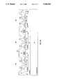
- FIGS. 8a and 8b cross-sectional views of an N-well CMOS embodiment of the integrating photosensor array of FIG. 7a using the integrating photosensor of FIGS. 2a and 2b are shown.
- FIG. 8a is oriented along an axis parallel to the rows of the array.
- the cross-section of FIG. 8a bisects a row-select line of the array.
- the axis of FIG. 8b is orthogonal to that of FIG. 8a, and thus runs parallel to a column of the array.
- the cross-section of FIG. 8b bisects a column sense line of the array.
- the portion of the array shown in FIGS. 8a and 8b includes three rows and three columns of integrating photosensors.
- FIGS. 8a and 8b will be the same as the reference numerals used for the same elements shown in FIG. 2b and 7a.
- array 80 is shown to include an exemplary row 82 of integrating photosensors including photosensors 10a, 10b, and 10c, fabricated in N-well 20, formed in p-type substrate 22 using conventional processing techniques.
- FIG. 7a illustrates a row including four integrating photosensors, only three photosensors 10a, 10b, and 10c are shown for simplicity in row 82 of FIG. 8a.
- Integrating photosensors 10a, 10b, and 10c may be separated by conventionally formed field oxide regions 26, as is well known in the art.
- P-type base regions 24a, 24b, and 24c formed in regions of N-well 20 between birds beaks or in apertures etched in a uniformly grown field oxide 26, comprise the base regions of the NPN bipolar transistors comprising integrating photosensors 10a, 10b, and 10c, respectively.
- the minimum inter-pixel distance is set by the inter-base spacing.
- the base doping is chosen such that the base surface concentration is larger than the well-surface concentration but light enough so that the base-emitter reverse leakage characteristic is not degraded by incipient breakdown at the reverse bias voltage used for integrating the photo-generated charge.
- N+ emitter regions 30a, 30b, and 30c form the emitters of bipolar transistor integrating photosensors 10a, 10b, and 10c, respectively.
- Conductive row-select line 16-1 comprises a line of conductive material, such as polysilicon, metal silicide or any other conductive layer which may be employed as a gate in a CMOS process. Row-select line 16-1 line runs the length of the row 82 over field oxide regions 26 and gate oxide regions 28a, 28b, and 28c. Deposited oxide layer 32 covers row-select line 16-1.
- Column sense lines 18-1, 18-2, and 18-3 are shown in end view disposed over deposited oxide layer 32 and contacting emitters 30a, 30b, and 30c of integrating photosensors 10a, 10b and 10c, respectively.
- FIG. 8b is a cross-sectional view taken along the first column of array 80 in a location which bisects metal column sense line 18-1 of FIG. 7a.
- Column sense line 18-1 is shown running the length of the column and contacting emitters 30a, 30e, and 30i of integrating photosensors 10a, 10e, and 10i.
- row-select line 16-1 appears to be discontinuous, those of ordinary skill in the art will recognize that this is because the axis of the cross section bisects apertures in row line 16-1 used to define the emitters 30a, 30b, and 30c of photosensors 10a, 10b, and 10c.
- Metal contact vias are used to connect emitters 30a, 30b, and 30c to their respective column sense lines. Examination of FIGS. 8a and 8b together reveals that the contact vias pass through continuous conductive row-select lines which are insulated from the metal column sense lines 18-1, 18-2, and 18-3 by deposited oxide 32 and from base regions 24a, 24b, and 24c by thin gate oxide regions 28a, 28b, 28c.
- FIGS. 8a and 8b Examination of both FIGS. 8a and 8b also reveals that the emitter regions are substantially self aligned to the edges of the polysilicon layers forming row-select lines 16-1, 16-2, and 16-3. This is a result of the fact that the emitter regions are created during the self-aligned gate source/drain implant step simultaneously with the sources and drains of the MOS transistors on the integrated circuit. Those of ordinary skill in the art will realize that this provides the advantage of minimizing the emitter-to-row-select-line capacitance in the integrating photosensors.
Abstract
Description
Claims (23)
Priority Applications (4)
| Application Number | Priority Date | Filing Date | Title |
|---|---|---|---|
| US07/760,569 US5260592A (en) | 1991-02-19 | 1991-09-16 | Integrating photosensor and imaging system having wide dynamic range with varactors |
| US07/923,734 US5324958A (en) | 1991-02-19 | 1992-07-30 | Integrating imaging systgem having wide dynamic range with sample/hold circuits |
| US07/927,079 US5289023A (en) | 1991-02-19 | 1992-08-07 | High-density photosensor and contactless imaging array having wide dynamic range |
| US08/746,439 US5763909A (en) | 1991-02-19 | 1996-11-08 | Integrating imaging system with phototransistor having wide dynamic range |
Applications Claiming Priority (2)
| Application Number | Priority Date | Filing Date | Title |
|---|---|---|---|
| US07/657,128 US5097305A (en) | 1991-02-19 | 1991-02-19 | Integrating photosensor and imaging system having wide dynamic range |
| US07/760,569 US5260592A (en) | 1991-02-19 | 1991-09-16 | Integrating photosensor and imaging system having wide dynamic range with varactors |
Related Parent Applications (1)
| Application Number | Title | Priority Date | Filing Date |
|---|---|---|---|
| US07/657,128 Continuation-In-Part US5097305A (en) | 1991-02-19 | 1991-02-19 | Integrating photosensor and imaging system having wide dynamic range |
Related Child Applications (1)
| Application Number | Title | Priority Date | Filing Date |
|---|---|---|---|
| US07/923,734 Continuation-In-Part US5324958A (en) | 1991-02-19 | 1992-07-30 | Integrating imaging systgem having wide dynamic range with sample/hold circuits |
Publications (1)
| Publication Number | Publication Date |
|---|---|
| US5260592A true US5260592A (en) | 1993-11-09 |
Family
ID=27097342
Family Applications (1)
| Application Number | Title | Priority Date | Filing Date |
|---|---|---|---|
| US07/760,569 Expired - Lifetime US5260592A (en) | 1991-02-19 | 1991-09-16 | Integrating photosensor and imaging system having wide dynamic range with varactors |
Country Status (1)
| Country | Link |
|---|---|
| US (1) | US5260592A (en) |
Cited By (91)
| Publication number | Priority date | Publication date | Assignee | Title |
|---|---|---|---|---|
| US5549762A (en) * | 1995-01-13 | 1996-08-27 | International Rectifier Corporation | Photovoltaic generator with dielectric isolation and bonded, insulated wafer layers |
| US5552619A (en) * | 1995-05-10 | 1996-09-03 | National Semiconductor Corporation | Capacitor coupled contactless imager with high resolution and wide dynamic range |
| US5557363A (en) * | 1993-03-16 | 1996-09-17 | Olympus Optical Co., Ltd. | CMOS-analog IC for controlling camera and camera system using the same |
| US5566044A (en) * | 1995-05-10 | 1996-10-15 | National Semiconductor Corporation | Base capacitor coupled photosensor with emitter tunnel oxide for very wide dynamic range in a contactless imaging array |
| US5712499A (en) * | 1994-11-08 | 1998-01-27 | Thomson-Csf | Large photodetector array |
| US5760458A (en) * | 1996-10-22 | 1998-06-02 | Foveonics, Inc. | Bipolar-based active pixel sensor cell with poly contact and increased capacitive coupling to the base region |
| US5763909A (en) * | 1991-02-19 | 1998-06-09 | Synaptics, Incorporated | Integrating imaging system with phototransistor having wide dynamic range |
| US5776795A (en) * | 1996-08-13 | 1998-07-07 | Foveonics, Inc. | Method of making a contactless capacitor-coupled bipolar active pixel sensor with intergrated electronic shutter |
| US5786623A (en) * | 1996-10-22 | 1998-07-28 | Foveonics, Inc. | Bipolar-based active pixel sensor cell with metal contact and increased capacitive coupling to the base region |
| US5844265A (en) * | 1996-07-11 | 1998-12-01 | Synaptics, Incorporated | Sense amplifier for high-density imaging array |
| US5847422A (en) * | 1997-05-19 | 1998-12-08 | Foveonics, Inc. | MOS-based active pixel sensor cell that utilizes the parasitic bipolar action of the cell to output image data |
| US5854100A (en) * | 1997-11-17 | 1998-12-29 | Vanguard International Semiconductor Corporation | Method of forming a new bipolar/CMOS pixel for high resolution imagers |
| US5932873A (en) * | 1996-08-13 | 1999-08-03 | Foveon, Inc. | Capacitor-coupled bipolar active pixel sensor with integrated electronic shutter |
| US6064053A (en) * | 1998-04-02 | 2000-05-16 | Vanguard International Semiconductor Corporation | Operation methods for active BiCMOS pixel for electronic shutter and image-lag elimination |
| US6088058A (en) * | 1997-05-29 | 2000-07-11 | Foveon, Inc. | Capacitive coupled bipolar active pixel imager having overflow protection and electronic shutter |
| US20020110376A1 (en) * | 2001-02-08 | 2002-08-15 | Maclean Steven D. | Method and apparatus for calibrating a sensor for highlights and for processing highlights |
| US6501109B1 (en) | 2001-08-29 | 2002-12-31 | Taiwan Semiconductor Manufacturing Company | Active CMOS pixel with exponential output based on the GIDL mechanism |
| US20030036265A1 (en) * | 2001-05-17 | 2003-02-20 | Optronx, Inc. | Integrated optical/electronic circuits and associated methods of simultaneous generation thereof |
| US6603889B2 (en) | 2001-05-17 | 2003-08-05 | Optronx, Inc. | Optical deflector apparatus and associated method |
| US6608945B2 (en) | 2001-05-17 | 2003-08-19 | Optronx, Inc. | Self-aligning modulator method and associated apparatus |
| US6625348B2 (en) | 2001-05-17 | 2003-09-23 | Optron X, Inc. | Programmable delay generator apparatus and associated method |
| US6690844B2 (en) | 2001-05-17 | 2004-02-10 | Optronx, Inc. | Optical fiber apparatus and associated method |
| US6748125B2 (en) | 2001-05-17 | 2004-06-08 | Sioptical, Inc. | Electronic semiconductor control of light in optical waveguide |
| US7253643B1 (en) | 2006-07-19 | 2007-08-07 | Cypress Semiconductor Corporation | Uninterrupted radial capacitive sense interface |
| US7307485B1 (en) | 2005-11-14 | 2007-12-11 | Cypress Semiconductor Corporation | Capacitance sensor using relaxation oscillators |
| US7312616B2 (en) | 2006-01-20 | 2007-12-25 | Cypress Semiconductor Corporation | Successive approximate capacitance measurement circuit |
| US20080007534A1 (en) * | 2006-07-10 | 2008-01-10 | Cypress Semiconductor Corporation | Touch-sensor with shared capacitive sensors |
| US20080179112A1 (en) * | 2007-01-30 | 2008-07-31 | Zheng Qin | Setting a discharge rate and a charge rate of a relaxation oscillator circuit |
| US20080277171A1 (en) * | 2007-05-07 | 2008-11-13 | Wright David G | Reducing sleep current in a capacitance sensing system |
| US7721609B2 (en) | 2006-03-31 | 2010-05-25 | Cypress Semiconductor Corporation | Method and apparatus for sensing the force with which a button is pressed |
| US7737724B2 (en) | 2007-04-17 | 2010-06-15 | Cypress Semiconductor Corporation | Universal digital block interconnection and channel routing |
| US7761845B1 (en) | 2002-09-09 | 2010-07-20 | Cypress Semiconductor Corporation | Method for parameterizing a user module |
| US7765095B1 (en) | 2000-10-26 | 2010-07-27 | Cypress Semiconductor Corporation | Conditional branching in an in-circuit emulation system |
| US7770113B1 (en) | 2001-11-19 | 2010-08-03 | Cypress Semiconductor Corporation | System and method for dynamically generating a configuration datasheet |
| US7774190B1 (en) | 2001-11-19 | 2010-08-10 | Cypress Semiconductor Corporation | Sleep and stall in an in-circuit emulation system |
| US7825688B1 (en) | 2000-10-26 | 2010-11-02 | Cypress Semiconductor Corporation | Programmable microcontroller architecture(mixed analog/digital) |
| US7844437B1 (en) | 2001-11-19 | 2010-11-30 | Cypress Semiconductor Corporation | System and method for performing next placements and pruning of disallowed placements for programming an integrated circuit |
| US7893724B2 (en) | 2004-03-25 | 2011-02-22 | Cypress Semiconductor Corporation | Method and circuit for rapid alignment of signals |
| US8026739B2 (en) | 2007-04-17 | 2011-09-27 | Cypress Semiconductor Corporation | System level interconnect with programmable switching |
| US8040142B1 (en) | 2006-03-31 | 2011-10-18 | Cypress Semiconductor Corporation | Touch detection techniques for capacitive touch sense systems |
| US8040266B2 (en) | 2007-04-17 | 2011-10-18 | Cypress Semiconductor Corporation | Programmable sigma-delta analog-to-digital converter |
| US8049569B1 (en) | 2007-09-05 | 2011-11-01 | Cypress Semiconductor Corporation | Circuit and method for improving the accuracy of a crystal-less oscillator having dual-frequency modes |
| US8050876B2 (en) | 2005-07-18 | 2011-11-01 | Analog Devices, Inc. | Automatic environmental compensation of capacitance based proximity sensors |
| US8069428B1 (en) | 2001-10-24 | 2011-11-29 | Cypress Semiconductor Corporation | Techniques for generating microcontroller configuration information |
| US8069436B2 (en) | 2004-08-13 | 2011-11-29 | Cypress Semiconductor Corporation | Providing hardware independence to automate code generation of processing device firmware |
| US8067948B2 (en) | 2006-03-27 | 2011-11-29 | Cypress Semiconductor Corporation | Input/output multiplexer bus |
| US8069405B1 (en) | 2001-11-19 | 2011-11-29 | Cypress Semiconductor Corporation | User interface for efficiently browsing an electronic document using data-driven tabs |
| US8078970B1 (en) | 2001-11-09 | 2011-12-13 | Cypress Semiconductor Corporation | Graphical user interface with user-selectable list-box |
| US8078894B1 (en) | 2007-04-25 | 2011-12-13 | Cypress Semiconductor Corporation | Power management architecture, method and configuration system |
| US8085067B1 (en) | 2005-12-21 | 2011-12-27 | Cypress Semiconductor Corporation | Differential-to-single ended signal converter circuit and method |
| US8086417B2 (en) | 2007-07-03 | 2011-12-27 | Cypress Semiconductor Corporation | Normalizing capacitive sensor array signals |
| US8085100B2 (en) | 2005-02-04 | 2011-12-27 | Cypress Semiconductor Corporation | Poly-phase frequency synthesis oscillator |
| US8089289B1 (en) | 2007-07-03 | 2012-01-03 | Cypress Semiconductor Corporation | Capacitive field sensor with sigma-delta modulator |
| US8089461B2 (en) | 2005-06-23 | 2012-01-03 | Cypress Semiconductor Corporation | Touch wake for electronic devices |
| US8089288B1 (en) | 2006-11-16 | 2012-01-03 | Cypress Semiconductor Corporation | Charge accumulation capacitance sensor with linear transfer characteristic |
| US8089472B2 (en) | 2006-05-26 | 2012-01-03 | Cypress Semiconductor Corporation | Bidirectional slider with delete function |
| US8092083B2 (en) | 2007-04-17 | 2012-01-10 | Cypress Semiconductor Corporation | Temperature sensor with digital bandgap |
| US8103497B1 (en) | 2002-03-28 | 2012-01-24 | Cypress Semiconductor Corporation | External interface for event architecture |
| US8103496B1 (en) | 2000-10-26 | 2012-01-24 | Cypress Semicondutor Corporation | Breakpoint control in an in-circuit emulation system |
| US8120408B1 (en) | 2005-05-05 | 2012-02-21 | Cypress Semiconductor Corporation | Voltage controlled oscillator delay cell and method |
| US8130025B2 (en) | 2007-04-17 | 2012-03-06 | Cypress Semiconductor Corporation | Numerical band gap |
| US8149048B1 (en) | 2000-10-26 | 2012-04-03 | Cypress Semiconductor Corporation | Apparatus and method for programmable power management in a programmable analog circuit block |
| US8160864B1 (en) | 2000-10-26 | 2012-04-17 | Cypress Semiconductor Corporation | In-circuit emulator and pod synchronized boot |
| US8169238B1 (en) | 2007-07-03 | 2012-05-01 | Cypress Semiconductor Corporation | Capacitance to frequency converter |
| US8176296B2 (en) | 2000-10-26 | 2012-05-08 | Cypress Semiconductor Corporation | Programmable microcontroller architecture |
| US8286125B2 (en) | 2004-08-13 | 2012-10-09 | Cypress Semiconductor Corporation | Model for a hardware device-independent method of defining embedded firmware for programmable systems |
| US8321174B1 (en) | 2008-09-26 | 2012-11-27 | Cypress Semiconductor Corporation | System and method to measure capacitance of capacitive sensor array |
| US8358142B2 (en) | 2008-02-27 | 2013-01-22 | Cypress Semiconductor Corporation | Methods and circuits for measuring mutual and self capacitance |
| US8402313B1 (en) | 2002-05-01 | 2013-03-19 | Cypress Semiconductor Corporation | Reconfigurable testing system and method |
| US8487912B1 (en) | 2008-02-01 | 2013-07-16 | Cypress Semiconductor Corporation | Capacitive sense touch device with hysteresis threshold |
| US8487639B1 (en) | 2008-11-21 | 2013-07-16 | Cypress Semiconductor Corporation | Receive demodulator for capacitive sensing |
| US8493351B2 (en) | 2006-03-30 | 2013-07-23 | Cypress Semiconductor Corporation | Apparatus and method for reducing average scan rate to detect a conductive object on a sensing device |
| US8499270B1 (en) | 2007-04-25 | 2013-07-30 | Cypress Semiconductor Corporation | Configuration of programmable IC design elements |
| US8516025B2 (en) | 2007-04-17 | 2013-08-20 | Cypress Semiconductor Corporation | Clock driven dynamic datapath chaining |
| US8525798B2 (en) | 2008-01-28 | 2013-09-03 | Cypress Semiconductor Corporation | Touch sensing |
| US8527949B1 (en) | 2001-11-19 | 2013-09-03 | Cypress Semiconductor Corporation | Graphical user interface for dynamically reconfiguring a programmable device |
| US8537121B2 (en) | 2006-05-26 | 2013-09-17 | Cypress Semiconductor Corporation | Multi-function slider in touchpad |
| US8564313B1 (en) | 2007-07-03 | 2013-10-22 | Cypress Semiconductor Corporation | Capacitive field sensor with sigma-delta modulator |
| US8570052B1 (en) | 2008-02-27 | 2013-10-29 | Cypress Semiconductor Corporation | Methods and circuits for measuring mutual and self capacitance |
| US8866500B2 (en) | 2009-03-26 | 2014-10-21 | Cypress Semiconductor Corporation | Multi-functional capacitance sensing circuit with a current conveyor |
| US9104273B1 (en) | 2008-02-29 | 2015-08-11 | Cypress Semiconductor Corporation | Multi-touch sensing method |
| US9154160B2 (en) | 2006-11-14 | 2015-10-06 | Cypress Semiconductor Corporation | Capacitance to code converter with sigma-delta modulator |
| US20150349186A1 (en) * | 2014-05-30 | 2015-12-03 | Wispro Technology Consulting Corporation Limited | Phototransistor with body-strapped base |
| US9268441B2 (en) | 2011-04-05 | 2016-02-23 | Parade Technologies, Ltd. | Active integrator for a capacitive sense array |
| US9448964B2 (en) | 2009-05-04 | 2016-09-20 | Cypress Semiconductor Corporation | Autonomous control in a programmable system |
| US9500686B1 (en) | 2007-06-29 | 2016-11-22 | Cypress Semiconductor Corporation | Capacitance measurement system and methods |
| US9507465B2 (en) | 2006-07-25 | 2016-11-29 | Cypress Semiconductor Corporation | Technique for increasing the sensitivity of capacitive sensor arrays |
| US9564902B2 (en) | 2007-04-17 | 2017-02-07 | Cypress Semiconductor Corporation | Dynamically configurable and re-configurable data path |
| US9720805B1 (en) | 2007-04-25 | 2017-08-01 | Cypress Semiconductor Corporation | System and method for controlling a target device |
| US9766738B1 (en) | 2006-08-23 | 2017-09-19 | Cypress Semiconductor Corporation | Position and usage based prioritization for capacitance sense interface |
| US10698662B2 (en) | 2001-11-15 | 2020-06-30 | Cypress Semiconductor Corporation | System providing automatic source code generation for personalization and parameterization of user modules |
Citations (31)
| Publication number | Priority date | Publication date | Assignee | Title |
|---|---|---|---|---|
| US3470318A (en) * | 1966-05-11 | 1969-09-30 | Webb James E | Solid state television camera system |
| US3617823A (en) * | 1969-03-07 | 1971-11-02 | Rca Corp | Self-scanned phototransistor array employing common substrate |
| US3909520A (en) * | 1969-10-14 | 1975-09-30 | Westinghouse Electric Corp | Readout system for a solid-state television camera |
| US3919469A (en) * | 1972-03-04 | 1975-11-11 | Philips Corp | Sensor provided with a pick-up panel |
| US3946151A (en) * | 1973-02-14 | 1976-03-23 | Hitachi, Ltd. | Semiconductor image sensor |
| US4139783A (en) * | 1975-09-02 | 1979-02-13 | General Electric Company | Single phase signal processing system utilizing charge transfer devices |
| US4156818A (en) * | 1975-12-23 | 1979-05-29 | International Business Machines Corporation | Operating circuitry for semiconductor charge coupled devices |
| US4224585A (en) * | 1978-08-28 | 1980-09-23 | Reticon Corporation | Methods and apparatus for compensating for charge transfer inefficiency in imaging and other variable length charge transfer devices |
| US4291224A (en) * | 1978-11-30 | 1981-09-22 | Nippon Kogaku K.K. | Light image space frequency component extracting device |
| US4434441A (en) * | 1980-11-27 | 1984-02-28 | Fujitsu Limited | Method for driving a charge injection device |
| EP0132076A1 (en) * | 1983-07-02 | 1985-01-23 | Canon Kabushiki Kaisha | Photoelectric converter |
| US4528684A (en) * | 1982-07-23 | 1985-07-09 | Tokyo Shibaura Denki Kabushiki Kaisha | Charge-coupled device output circuit |
| US4556800A (en) * | 1982-04-02 | 1985-12-03 | Nippon Telegraph & Telephone Public Corp. | Optical image sensor apparatus with grouped photosensors connected in common |
| US4682203A (en) * | 1984-08-23 | 1987-07-21 | Fuji Photo Film Co., Ltd. | Solid-state image pickup device with photographic sensitivity characteristics |
| US4737832A (en) * | 1985-04-01 | 1988-04-12 | Canon Kabushiki Kaisha | Optical signal processor |
| US4780605A (en) * | 1987-11-16 | 1988-10-25 | General Electric Company | Coherent light phase detecting focal plane charge-transfer-device |
| US4783694A (en) * | 1984-03-16 | 1988-11-08 | Motorola Inc. | Integrated bipolar-MOS semiconductor device with common collector and drain |
| US4786818A (en) * | 1987-11-09 | 1988-11-22 | California Institute Of Technology | Integrated sensor and processor for visual images |
| US4797560A (en) * | 1986-01-20 | 1989-01-10 | Thomson-Csf | Matrix of photosensitive elements and an associated reading method in image formation |
| US4814846A (en) * | 1985-06-12 | 1989-03-21 | Canon Kabushiki Kaisha | Photoelectric converting device |
| US4847668A (en) * | 1985-11-13 | 1989-07-11 | Canon Kabushiki Kaisha | Device and method of photoelectrically converting light into electrical signal |
| US4876534A (en) * | 1988-02-05 | 1989-10-24 | Synaptics Incorporated | Scanning method and apparatus for current signals having large dynamic range |
| US4907059A (en) * | 1985-01-30 | 1990-03-06 | Kabushiki Kaisha Toshiba | Semiconductor bipolar-CMOS inverter |
| US4906855A (en) * | 1988-02-26 | 1990-03-06 | Thomson-Csf | Photosensitive matrix with two diodes per dot without specific resetting conductor |
| US4948966A (en) * | 1988-09-16 | 1990-08-14 | Thomson-Csf | Method for the reading of photosensitive cells of the type comprising two series-mounted diodes with different directions of conduction |
| US4952788A (en) * | 1988-10-14 | 1990-08-28 | Thomson-Csf | Method of photoelectric detection with reduction of remanence of a phototransistor, notably of the NIPIN type |
| US4959723A (en) * | 1987-11-06 | 1990-09-25 | Canon Kabushiki Kaisha | Solid state image pickup apparatus having multi-phase scanning pulse to read out accumulated signal |
| US4972243A (en) * | 1986-09-19 | 1990-11-20 | Canon Kabushiki Kaisha | Photoelectric conversion apparatus with shielded cell |
| WO1991004633A1 (en) * | 1989-09-23 | 1991-04-04 | Vlsi Vision Limited | I.c. sensor |
| US5097305A (en) * | 1991-02-19 | 1992-03-17 | Synaptics Corporation | Integrating photosensor and imaging system having wide dynamic range |
| US5132541A (en) * | 1990-01-27 | 1992-07-21 | U.S. Philips Corporation | Sensor matrix |
-
1991
- 1991-09-16 US US07/760,569 patent/US5260592A/en not_active Expired - Lifetime
Patent Citations (31)
| Publication number | Priority date | Publication date | Assignee | Title |
|---|---|---|---|---|
| US3470318A (en) * | 1966-05-11 | 1969-09-30 | Webb James E | Solid state television camera system |
| US3617823A (en) * | 1969-03-07 | 1971-11-02 | Rca Corp | Self-scanned phototransistor array employing common substrate |
| US3909520A (en) * | 1969-10-14 | 1975-09-30 | Westinghouse Electric Corp | Readout system for a solid-state television camera |
| US3919469A (en) * | 1972-03-04 | 1975-11-11 | Philips Corp | Sensor provided with a pick-up panel |
| US3946151A (en) * | 1973-02-14 | 1976-03-23 | Hitachi, Ltd. | Semiconductor image sensor |
| US4139783A (en) * | 1975-09-02 | 1979-02-13 | General Electric Company | Single phase signal processing system utilizing charge transfer devices |
| US4156818A (en) * | 1975-12-23 | 1979-05-29 | International Business Machines Corporation | Operating circuitry for semiconductor charge coupled devices |
| US4224585A (en) * | 1978-08-28 | 1980-09-23 | Reticon Corporation | Methods and apparatus for compensating for charge transfer inefficiency in imaging and other variable length charge transfer devices |
| US4291224A (en) * | 1978-11-30 | 1981-09-22 | Nippon Kogaku K.K. | Light image space frequency component extracting device |
| US4434441A (en) * | 1980-11-27 | 1984-02-28 | Fujitsu Limited | Method for driving a charge injection device |
| US4556800A (en) * | 1982-04-02 | 1985-12-03 | Nippon Telegraph & Telephone Public Corp. | Optical image sensor apparatus with grouped photosensors connected in common |
| US4528684A (en) * | 1982-07-23 | 1985-07-09 | Tokyo Shibaura Denki Kabushiki Kaisha | Charge-coupled device output circuit |
| EP0132076A1 (en) * | 1983-07-02 | 1985-01-23 | Canon Kabushiki Kaisha | Photoelectric converter |
| US4783694A (en) * | 1984-03-16 | 1988-11-08 | Motorola Inc. | Integrated bipolar-MOS semiconductor device with common collector and drain |
| US4682203A (en) * | 1984-08-23 | 1987-07-21 | Fuji Photo Film Co., Ltd. | Solid-state image pickup device with photographic sensitivity characteristics |
| US4907059A (en) * | 1985-01-30 | 1990-03-06 | Kabushiki Kaisha Toshiba | Semiconductor bipolar-CMOS inverter |
| US4737832A (en) * | 1985-04-01 | 1988-04-12 | Canon Kabushiki Kaisha | Optical signal processor |
| US4814846A (en) * | 1985-06-12 | 1989-03-21 | Canon Kabushiki Kaisha | Photoelectric converting device |
| US4847668A (en) * | 1985-11-13 | 1989-07-11 | Canon Kabushiki Kaisha | Device and method of photoelectrically converting light into electrical signal |
| US4797560A (en) * | 1986-01-20 | 1989-01-10 | Thomson-Csf | Matrix of photosensitive elements and an associated reading method in image formation |
| US4972243A (en) * | 1986-09-19 | 1990-11-20 | Canon Kabushiki Kaisha | Photoelectric conversion apparatus with shielded cell |
| US4959723A (en) * | 1987-11-06 | 1990-09-25 | Canon Kabushiki Kaisha | Solid state image pickup apparatus having multi-phase scanning pulse to read out accumulated signal |
| US4786818A (en) * | 1987-11-09 | 1988-11-22 | California Institute Of Technology | Integrated sensor and processor for visual images |
| US4780605A (en) * | 1987-11-16 | 1988-10-25 | General Electric Company | Coherent light phase detecting focal plane charge-transfer-device |
| US4876534A (en) * | 1988-02-05 | 1989-10-24 | Synaptics Incorporated | Scanning method and apparatus for current signals having large dynamic range |
| US4906855A (en) * | 1988-02-26 | 1990-03-06 | Thomson-Csf | Photosensitive matrix with two diodes per dot without specific resetting conductor |
| US4948966A (en) * | 1988-09-16 | 1990-08-14 | Thomson-Csf | Method for the reading of photosensitive cells of the type comprising two series-mounted diodes with different directions of conduction |
| US4952788A (en) * | 1988-10-14 | 1990-08-28 | Thomson-Csf | Method of photoelectric detection with reduction of remanence of a phototransistor, notably of the NIPIN type |
| WO1991004633A1 (en) * | 1989-09-23 | 1991-04-04 | Vlsi Vision Limited | I.c. sensor |
| US5132541A (en) * | 1990-01-27 | 1992-07-21 | U.S. Philips Corporation | Sensor matrix |
| US5097305A (en) * | 1991-02-19 | 1992-03-17 | Synaptics Corporation | Integrating photosensor and imaging system having wide dynamic range |
Non-Patent Citations (20)
| Title |
|---|
| "A Solid-State Image Converter" IEE Transactions on Electron Devices, Richard Stewart, vol. ED-15, No. 4, Apr. 1968, pp. 220-225. |
| A Solid State Image Converter IEE Transactions on Electron Devices, Richard Stewart, vol. ED 15, No. 4, Apr. 1968, pp. 220 225. * |
| Anders, et al., "Developmental Solid State Imaging System," IEEE Transactions on Electron Devices, vol. ED-15, No. 4, Apr. 1968, pp. 191-195. |
| Anders, et al., Developmental Solid State Imaging System, IEEE Transactions on Electron Devices, vol. ED 15, No. 4, Apr. 1968, pp. 191 195. * |
| Callahan, et al., "Performance Characteristics of Pulsed Phototransistor Structures Under Various Conditions", IEEE Transactions of Electron Devices, vol. ED∝15, No. 4, Apr. 1968, pp. 248-256. |
| Callahan, et al., Performance Characteristics of Pulsed Phototransistor Structures Under Various Conditions , IEEE Transactions of Electron Devices, vol. ED 15, No. 4, Apr. 1968, pp. 248 256. * |
| Dyck and Weckler, "Integrated Arrays of Silicon Photodetectors for Imaging Sensing", IEEE Transactions on Electron Devices, vol. ED-15, No. 4 Apr. 1968, pp. 196-201. |
| Dyck and Weckler, Integrated Arrays of Silicon Photodetectors for Imaging Sensing , IEEE Transactions on Electron Devices, vol. ED 15, No. 4 Apr. 1968, pp. 196 201. * |
| Joy, et al., "Phototransistor Operation in the Charge Storage Mode", IEEE Transactions On Electron Devices, vol. ED-15, No. 4, Apr. 1968, pp. 237-248. |
| Joy, et al., Phototransistor Operation in the Charge Storage Mode , IEEE Transactions On Electron Devices, vol. ED 15, No. 4, Apr. 1968, pp. 237 248. * |
| List, "Solid State Imaging--Methods of Approach," IEEE Transactions on Electron Devices, vol. ED-15, No. 4, Apr. 1968, pp. 256-261. |
| List, Solid State Imaging Methods of Approach, IEEE Transactions on Electron Devices, vol. ED 15, No. 4, Apr. 1968, pp. 256 261. * |
| Noble, Self Scanned Silicon Image Detector Arrays, IEEE Transactions on Electron Devices, vol. ED 15, No. 4, Apr. 1968, pp. 202 209. * |
| Noble, Self-Scanned Silicon Image Detector Arrays, IEEE Transactions on Electron Devices, vol. ED-15, No. 4, Apr. 1968, pp. 202-209. |
| Sadasiv, et al., "T in-Film Circuits for Scanning Image-Sensor Arrays," IEEE Transactions on Electron Devices, vol. ED-15, No. 4, Apr. 1968, pp. 215-219. |
| Sadasiv, et al., T in Film Circuits for Scanning Image Sensor Arrays, IEEE Transactions on Electron Devices, vol. ED 15, No. 4, Apr. 1968, pp. 215 219. * |
| Soref, "Monolithic Silicon Mosaics for Fae-Infrared Imaging," IEEE Transactions on Electron Devices, vol. ED-15, No. 4, Apr. 1968, pp. 209-214. |
| Soref, Monolithic Silicon Mosaics for Fae Infrared Imaging, IEEE Transactions on Electron Devices, vol. ED 15, No. 4, Apr. 1968, pp. 209 214. * |
| Tepper, et al., "Transfer Functions of Imaging Mosaics Utilizing the Charge Storage Phenomena of Transistor Structures," IEE Transactions on Electron Devices, vol. ED-15, No. 4, Apr. 1968, pp. 226-237. |
| Tepper, et al., Transfer Functions of Imaging Mosaics Utilizing the Charge Storage Phenomena of Transistor Structures, IEE Transactions on Electron Devices, vol. ED 15, No. 4, Apr. 1968, pp. 226 237. * |
Cited By (142)
| Publication number | Priority date | Publication date | Assignee | Title |
|---|---|---|---|---|
| US5763909A (en) * | 1991-02-19 | 1998-06-09 | Synaptics, Incorporated | Integrating imaging system with phototransistor having wide dynamic range |
| US5557363A (en) * | 1993-03-16 | 1996-09-17 | Olympus Optical Co., Ltd. | CMOS-analog IC for controlling camera and camera system using the same |
| US5708880A (en) * | 1993-03-16 | 1998-01-13 | Olympus Optical Co., Ltd. | CMOS-analog IC for controlling camera and camera system using the same |
| US5712499A (en) * | 1994-11-08 | 1998-01-27 | Thomson-Csf | Large photodetector array |
| US5549762A (en) * | 1995-01-13 | 1996-08-27 | International Rectifier Corporation | Photovoltaic generator with dielectric isolation and bonded, insulated wafer layers |
| US5552619A (en) * | 1995-05-10 | 1996-09-03 | National Semiconductor Corporation | Capacitor coupled contactless imager with high resolution and wide dynamic range |
| US5566044A (en) * | 1995-05-10 | 1996-10-15 | National Semiconductor Corporation | Base capacitor coupled photosensor with emitter tunnel oxide for very wide dynamic range in a contactless imaging array |
| US5844265A (en) * | 1996-07-11 | 1998-12-01 | Synaptics, Incorporated | Sense amplifier for high-density imaging array |
| US6097432A (en) * | 1996-07-11 | 2000-08-01 | Synaptics, Inc. | Sense amplifier for high-density imaging array |
| US5776795A (en) * | 1996-08-13 | 1998-07-07 | Foveonics, Inc. | Method of making a contactless capacitor-coupled bipolar active pixel sensor with intergrated electronic shutter |
| US5932873A (en) * | 1996-08-13 | 1999-08-03 | Foveon, Inc. | Capacitor-coupled bipolar active pixel sensor with integrated electronic shutter |
| US5786623A (en) * | 1996-10-22 | 1998-07-28 | Foveonics, Inc. | Bipolar-based active pixel sensor cell with metal contact and increased capacitive coupling to the base region |
| US6080601A (en) * | 1996-10-22 | 2000-06-27 | National Semiconductor Corporation | Method for forming a bipolar-based active pixel sensor cell with metal contact and increased capacitive coupling to the base region |
| US5760458A (en) * | 1996-10-22 | 1998-06-02 | Foveonics, Inc. | Bipolar-based active pixel sensor cell with poly contact and increased capacitive coupling to the base region |
| US6136635A (en) * | 1996-10-22 | 2000-10-24 | Foveonics, Inc. | Method for forming a bipolar-based active pixel sensor cell with poly contact and increased capacitive coupling to the base region |
| US5847422A (en) * | 1997-05-19 | 1998-12-08 | Foveonics, Inc. | MOS-based active pixel sensor cell that utilizes the parasitic bipolar action of the cell to output image data |
| US6088058A (en) * | 1997-05-29 | 2000-07-11 | Foveon, Inc. | Capacitive coupled bipolar active pixel imager having overflow protection and electronic shutter |
| US5854100A (en) * | 1997-11-17 | 1998-12-29 | Vanguard International Semiconductor Corporation | Method of forming a new bipolar/CMOS pixel for high resolution imagers |
| US6064053A (en) * | 1998-04-02 | 2000-05-16 | Vanguard International Semiconductor Corporation | Operation methods for active BiCMOS pixel for electronic shutter and image-lag elimination |
| US8736303B2 (en) | 2000-10-26 | 2014-05-27 | Cypress Semiconductor Corporation | PSOC architecture |
| US8358150B1 (en) | 2000-10-26 | 2013-01-22 | Cypress Semiconductor Corporation | Programmable microcontroller architecture(mixed analog/digital) |
| US8149048B1 (en) | 2000-10-26 | 2012-04-03 | Cypress Semiconductor Corporation | Apparatus and method for programmable power management in a programmable analog circuit block |
| US9766650B2 (en) | 2000-10-26 | 2017-09-19 | Cypress Semiconductor Corporation | Microcontroller programmable system on a chip with programmable interconnect |
| US9843327B1 (en) | 2000-10-26 | 2017-12-12 | Cypress Semiconductor Corporation | PSOC architecture |
| US8555032B2 (en) | 2000-10-26 | 2013-10-08 | Cypress Semiconductor Corporation | Microcontroller programmable system on a chip with programmable interconnect |
| US7825688B1 (en) | 2000-10-26 | 2010-11-02 | Cypress Semiconductor Corporation | Programmable microcontroller architecture(mixed analog/digital) |
| US7765095B1 (en) | 2000-10-26 | 2010-07-27 | Cypress Semiconductor Corporation | Conditional branching in an in-circuit emulation system |
| US8176296B2 (en) | 2000-10-26 | 2012-05-08 | Cypress Semiconductor Corporation | Programmable microcontroller architecture |
| US10020810B2 (en) | 2000-10-26 | 2018-07-10 | Cypress Semiconductor Corporation | PSoC architecture |
| US10248604B2 (en) | 2000-10-26 | 2019-04-02 | Cypress Semiconductor Corporation | Microcontroller programmable system on a chip |
| US10261932B2 (en) | 2000-10-26 | 2019-04-16 | Cypress Semiconductor Corporation | Microcontroller programmable system on a chip |
| US8103496B1 (en) | 2000-10-26 | 2012-01-24 | Cypress Semicondutor Corporation | Breakpoint control in an in-circuit emulation system |
| US8160864B1 (en) | 2000-10-26 | 2012-04-17 | Cypress Semiconductor Corporation | In-circuit emulator and pod synchronized boot |
| US10725954B2 (en) | 2000-10-26 | 2020-07-28 | Monterey Research, Llc | Microcontroller programmable system on a chip |
| US20060256214A1 (en) * | 2001-02-08 | 2006-11-16 | Maclean Steven D | Improving the highlight reproduction of an imaging system |
| US7088388B2 (en) | 2001-02-08 | 2006-08-08 | Eastman Kodak Company | Method and apparatus for calibrating a sensor for highlights and for processing highlights |
| US20020110376A1 (en) * | 2001-02-08 | 2002-08-15 | Maclean Steven D. | Method and apparatus for calibrating a sensor for highlights and for processing highlights |
| US6895136B2 (en) | 2001-05-17 | 2005-05-17 | Sioptical, Inc. | Integrated optical/electronic circuits and associated methods of simultaneous generation thereof |
| US6625348B2 (en) | 2001-05-17 | 2003-09-23 | Optron X, Inc. | Programmable delay generator apparatus and associated method |
| US20030036265A1 (en) * | 2001-05-17 | 2003-02-20 | Optronx, Inc. | Integrated optical/electronic circuits and associated methods of simultaneous generation thereof |
| US20040258348A1 (en) * | 2001-05-17 | 2004-12-23 | Shrenik Deliwala | Integrated optical/electronic circuits and associated methods of simultaneous generation thereof |
| US6826320B2 (en) | 2001-05-17 | 2004-11-30 | Sioptical, Inc. | Focusing mirror and lens |
| US6748125B2 (en) | 2001-05-17 | 2004-06-08 | Sioptical, Inc. | Electronic semiconductor control of light in optical waveguide |
| US6690844B2 (en) | 2001-05-17 | 2004-02-10 | Optronx, Inc. | Optical fiber apparatus and associated method |
| US6912330B2 (en) | 2001-05-17 | 2005-06-28 | Sioptical Inc. | Integrated optical/electronic circuits and associated methods of simultaneous generation thereof |
| US20030040175A1 (en) * | 2001-05-17 | 2003-02-27 | Optronx, Inc. | Hybrid active and electronic circuit with evanescent coupling |
| US6603889B2 (en) | 2001-05-17 | 2003-08-05 | Optronx, Inc. | Optical deflector apparatus and associated method |
| US6608945B2 (en) | 2001-05-17 | 2003-08-19 | Optronx, Inc. | Self-aligning modulator method and associated apparatus |
| US6501109B1 (en) | 2001-08-29 | 2002-12-31 | Taiwan Semiconductor Manufacturing Company | Active CMOS pixel with exponential output based on the GIDL mechanism |
| US8069428B1 (en) | 2001-10-24 | 2011-11-29 | Cypress Semiconductor Corporation | Techniques for generating microcontroller configuration information |
| US10466980B2 (en) | 2001-10-24 | 2019-11-05 | Cypress Semiconductor Corporation | Techniques for generating microcontroller configuration information |
| US8793635B1 (en) | 2001-10-24 | 2014-07-29 | Cypress Semiconductor Corporation | Techniques for generating microcontroller configuration information |
| US8078970B1 (en) | 2001-11-09 | 2011-12-13 | Cypress Semiconductor Corporation | Graphical user interface with user-selectable list-box |
| US10698662B2 (en) | 2001-11-15 | 2020-06-30 | Cypress Semiconductor Corporation | System providing automatic source code generation for personalization and parameterization of user modules |
| US7774190B1 (en) | 2001-11-19 | 2010-08-10 | Cypress Semiconductor Corporation | Sleep and stall in an in-circuit emulation system |
| US7770113B1 (en) | 2001-11-19 | 2010-08-03 | Cypress Semiconductor Corporation | System and method for dynamically generating a configuration datasheet |
| US8370791B2 (en) | 2001-11-19 | 2013-02-05 | Cypress Semiconductor Corporation | System and method for performing next placements and pruning of disallowed placements for programming an integrated circuit |
| US8533677B1 (en) | 2001-11-19 | 2013-09-10 | Cypress Semiconductor Corporation | Graphical user interface for dynamically reconfiguring a programmable device |
| US8069405B1 (en) | 2001-11-19 | 2011-11-29 | Cypress Semiconductor Corporation | User interface for efficiently browsing an electronic document using data-driven tabs |
| US7844437B1 (en) | 2001-11-19 | 2010-11-30 | Cypress Semiconductor Corporation | System and method for performing next placements and pruning of disallowed placements for programming an integrated circuit |
| US8527949B1 (en) | 2001-11-19 | 2013-09-03 | Cypress Semiconductor Corporation | Graphical user interface for dynamically reconfiguring a programmable device |
| US8103497B1 (en) | 2002-03-28 | 2012-01-24 | Cypress Semiconductor Corporation | External interface for event architecture |
| US8402313B1 (en) | 2002-05-01 | 2013-03-19 | Cypress Semiconductor Corporation | Reconfigurable testing system and method |
| US7761845B1 (en) | 2002-09-09 | 2010-07-20 | Cypress Semiconductor Corporation | Method for parameterizing a user module |
| US7893724B2 (en) | 2004-03-25 | 2011-02-22 | Cypress Semiconductor Corporation | Method and circuit for rapid alignment of signals |
| US8069436B2 (en) | 2004-08-13 | 2011-11-29 | Cypress Semiconductor Corporation | Providing hardware independence to automate code generation of processing device firmware |
| US8286125B2 (en) | 2004-08-13 | 2012-10-09 | Cypress Semiconductor Corporation | Model for a hardware device-independent method of defining embedded firmware for programmable systems |
| US8085100B2 (en) | 2005-02-04 | 2011-12-27 | Cypress Semiconductor Corporation | Poly-phase frequency synthesis oscillator |
| US8120408B1 (en) | 2005-05-05 | 2012-02-21 | Cypress Semiconductor Corporation | Voltage controlled oscillator delay cell and method |
| US8089461B2 (en) | 2005-06-23 | 2012-01-03 | Cypress Semiconductor Corporation | Touch wake for electronic devices |
| US8050876B2 (en) | 2005-07-18 | 2011-11-01 | Analog Devices, Inc. | Automatic environmental compensation of capacitance based proximity sensors |
| US7307485B1 (en) | 2005-11-14 | 2007-12-11 | Cypress Semiconductor Corporation | Capacitance sensor using relaxation oscillators |
| US8085067B1 (en) | 2005-12-21 | 2011-12-27 | Cypress Semiconductor Corporation | Differential-to-single ended signal converter circuit and method |
| US7884621B2 (en) | 2006-01-20 | 2011-02-08 | Cypress Semiconductor Corporation | Successive approximate capacitance measurement circuit |
| US7312616B2 (en) | 2006-01-20 | 2007-12-25 | Cypress Semiconductor Corporation | Successive approximate capacitance measurement circuit |
| US8717042B1 (en) | 2006-03-27 | 2014-05-06 | Cypress Semiconductor Corporation | Input/output multiplexer bus |
| US8067948B2 (en) | 2006-03-27 | 2011-11-29 | Cypress Semiconductor Corporation | Input/output multiplexer bus |
| US9152284B1 (en) | 2006-03-30 | 2015-10-06 | Cypress Semiconductor Corporation | Apparatus and method for reducing average scan rate to detect a conductive object on a sensing device |
| US8493351B2 (en) | 2006-03-30 | 2013-07-23 | Cypress Semiconductor Corporation | Apparatus and method for reducing average scan rate to detect a conductive object on a sensing device |
| US8040142B1 (en) | 2006-03-31 | 2011-10-18 | Cypress Semiconductor Corporation | Touch detection techniques for capacitive touch sense systems |
| US9494627B1 (en) | 2006-03-31 | 2016-11-15 | Monterey Research, Llc | Touch detection techniques for capacitive touch sense systems |
| US7721609B2 (en) | 2006-03-31 | 2010-05-25 | Cypress Semiconductor Corporation | Method and apparatus for sensing the force with which a button is pressed |
| US8248084B2 (en) | 2006-03-31 | 2012-08-21 | Cypress Semiconductor Corporation | Touch detection techniques for capacitive touch sense systems |
| US8089472B2 (en) | 2006-05-26 | 2012-01-03 | Cypress Semiconductor Corporation | Bidirectional slider with delete function |
| US8537121B2 (en) | 2006-05-26 | 2013-09-17 | Cypress Semiconductor Corporation | Multi-function slider in touchpad |
| US8040321B2 (en) | 2006-07-10 | 2011-10-18 | Cypress Semiconductor Corporation | Touch-sensor with shared capacitive sensors |
| US20080007534A1 (en) * | 2006-07-10 | 2008-01-10 | Cypress Semiconductor Corporation | Touch-sensor with shared capacitive sensors |
| US7253643B1 (en) | 2006-07-19 | 2007-08-07 | Cypress Semiconductor Corporation | Uninterrupted radial capacitive sense interface |
| US9507465B2 (en) | 2006-07-25 | 2016-11-29 | Cypress Semiconductor Corporation | Technique for increasing the sensitivity of capacitive sensor arrays |
| US10133432B2 (en) | 2006-07-25 | 2018-11-20 | Cypress Semiconductor Corporation | Technique for increasing the sensitivity of capacitive sense arrays |
| US9766738B1 (en) | 2006-08-23 | 2017-09-19 | Cypress Semiconductor Corporation | Position and usage based prioritization for capacitance sense interface |
| US9166621B2 (en) | 2006-11-14 | 2015-10-20 | Cypress Semiconductor Corporation | Capacitance to code converter with sigma-delta modulator |
| US9154160B2 (en) | 2006-11-14 | 2015-10-06 | Cypress Semiconductor Corporation | Capacitance to code converter with sigma-delta modulator |
| US8089288B1 (en) | 2006-11-16 | 2012-01-03 | Cypress Semiconductor Corporation | Charge accumulation capacitance sensor with linear transfer characteristic |
| US20080179112A1 (en) * | 2007-01-30 | 2008-07-31 | Zheng Qin | Setting a discharge rate and a charge rate of a relaxation oscillator circuit |
| US8058937B2 (en) | 2007-01-30 | 2011-11-15 | Cypress Semiconductor Corporation | Setting a discharge rate and a charge rate of a relaxation oscillator circuit |
| US9564902B2 (en) | 2007-04-17 | 2017-02-07 | Cypress Semiconductor Corporation | Dynamically configurable and re-configurable data path |
| US7737724B2 (en) | 2007-04-17 | 2010-06-15 | Cypress Semiconductor Corporation | Universal digital block interconnection and channel routing |
| US8026739B2 (en) | 2007-04-17 | 2011-09-27 | Cypress Semiconductor Corporation | System level interconnect with programmable switching |
| US8092083B2 (en) | 2007-04-17 | 2012-01-10 | Cypress Semiconductor Corporation | Temperature sensor with digital bandgap |
| US8476928B1 (en) | 2007-04-17 | 2013-07-02 | Cypress Semiconductor Corporation | System level interconnect with programmable switching |
| US8130025B2 (en) | 2007-04-17 | 2012-03-06 | Cypress Semiconductor Corporation | Numerical band gap |
| US8516025B2 (en) | 2007-04-17 | 2013-08-20 | Cypress Semiconductor Corporation | Clock driven dynamic datapath chaining |
| US8040266B2 (en) | 2007-04-17 | 2011-10-18 | Cypress Semiconductor Corporation | Programmable sigma-delta analog-to-digital converter |
| US8078894B1 (en) | 2007-04-25 | 2011-12-13 | Cypress Semiconductor Corporation | Power management architecture, method and configuration system |
| US9720805B1 (en) | 2007-04-25 | 2017-08-01 | Cypress Semiconductor Corporation | System and method for controlling a target device |
| US8499270B1 (en) | 2007-04-25 | 2013-07-30 | Cypress Semiconductor Corporation | Configuration of programmable IC design elements |
| US8909960B1 (en) | 2007-04-25 | 2014-12-09 | Cypress Semiconductor Corporation | Power management architecture, method and configuration system |
| US8144126B2 (en) | 2007-05-07 | 2012-03-27 | Cypress Semiconductor Corporation | Reducing sleep current in a capacitance sensing system |
| US10788937B2 (en) | 2007-05-07 | 2020-09-29 | Cypress Semiconductor Corporation | Reducing sleep current in a capacitance sensing system |
| US8976124B1 (en) | 2007-05-07 | 2015-03-10 | Cypress Semiconductor Corporation | Reducing sleep current in a capacitance sensing system |
| US20080277171A1 (en) * | 2007-05-07 | 2008-11-13 | Wright David G | Reducing sleep current in a capacitance sensing system |
| US9500686B1 (en) | 2007-06-29 | 2016-11-22 | Cypress Semiconductor Corporation | Capacitance measurement system and methods |
| US8089289B1 (en) | 2007-07-03 | 2012-01-03 | Cypress Semiconductor Corporation | Capacitive field sensor with sigma-delta modulator |
| US8536902B1 (en) * | 2007-07-03 | 2013-09-17 | Cypress Semiconductor Corporation | Capacitance to frequency converter |
| USRE46317E1 (en) | 2007-07-03 | 2017-02-21 | Monterey Research, Llc | Normalizing capacitive sensor array signals |
| US8169238B1 (en) | 2007-07-03 | 2012-05-01 | Cypress Semiconductor Corporation | Capacitance to frequency converter |
| US8570053B1 (en) | 2007-07-03 | 2013-10-29 | Cypress Semiconductor Corporation | Capacitive field sensor with sigma-delta modulator |
| US8315832B1 (en) | 2007-07-03 | 2012-11-20 | Cypress Semiconductor Corporation | Normalizing capacitive sensor array signals |
| US8086417B2 (en) | 2007-07-03 | 2011-12-27 | Cypress Semiconductor Corporation | Normalizing capacitive sensor array signals |
| US8564313B1 (en) | 2007-07-03 | 2013-10-22 | Cypress Semiconductor Corporation | Capacitive field sensor with sigma-delta modulator |
| US8049569B1 (en) | 2007-09-05 | 2011-11-01 | Cypress Semiconductor Corporation | Circuit and method for improving the accuracy of a crystal-less oscillator having dual-frequency modes |
| US8525798B2 (en) | 2008-01-28 | 2013-09-03 | Cypress Semiconductor Corporation | Touch sensing |
| US9760192B2 (en) | 2008-01-28 | 2017-09-12 | Cypress Semiconductor Corporation | Touch sensing |
| US8487912B1 (en) | 2008-02-01 | 2013-07-16 | Cypress Semiconductor Corporation | Capacitive sense touch device with hysteresis threshold |
| US9494628B1 (en) | 2008-02-27 | 2016-11-15 | Parade Technologies, Ltd. | Methods and circuits for measuring mutual and self capacitance |
| US8570052B1 (en) | 2008-02-27 | 2013-10-29 | Cypress Semiconductor Corporation | Methods and circuits for measuring mutual and self capacitance |
| US9423427B2 (en) | 2008-02-27 | 2016-08-23 | Parade Technologies, Ltd. | Methods and circuits for measuring mutual and self capacitance |
| US8358142B2 (en) | 2008-02-27 | 2013-01-22 | Cypress Semiconductor Corporation | Methods and circuits for measuring mutual and self capacitance |
| US8692563B1 (en) | 2008-02-27 | 2014-04-08 | Cypress Semiconductor Corporation | Methods and circuits for measuring mutual and self capacitance |
| US9104273B1 (en) | 2008-02-29 | 2015-08-11 | Cypress Semiconductor Corporation | Multi-touch sensing method |
| US11029795B2 (en) | 2008-09-26 | 2021-06-08 | Cypress Semiconductor Corporation | System and method to measure capacitance of capacitive sensor array |
| US8321174B1 (en) | 2008-09-26 | 2012-11-27 | Cypress Semiconductor Corporation | System and method to measure capacitance of capacitive sensor array |
| US10386969B1 (en) | 2008-09-26 | 2019-08-20 | Cypress Semiconductor Corporation | System and method to measure capacitance of capacitive sensor array |
| US8575947B1 (en) | 2008-11-21 | 2013-11-05 | Cypress Semiconductor Corporation | Receive demodulator for capacitive sensing |
| US8487639B1 (en) | 2008-11-21 | 2013-07-16 | Cypress Semiconductor Corporation | Receive demodulator for capacitive sensing |
| US8866500B2 (en) | 2009-03-26 | 2014-10-21 | Cypress Semiconductor Corporation | Multi-functional capacitance sensing circuit with a current conveyor |
| US9442146B2 (en) | 2009-03-26 | 2016-09-13 | Parade Technologies, Ltd. | Multi-mode capacitive sensing device and method with current conveyor |
| US9448964B2 (en) | 2009-05-04 | 2016-09-20 | Cypress Semiconductor Corporation | Autonomous control in a programmable system |
| US9268441B2 (en) | 2011-04-05 | 2016-02-23 | Parade Technologies, Ltd. | Active integrator for a capacitive sense array |
| US10553633B2 (en) * | 2014-05-30 | 2020-02-04 | Klaus Y.J. Hsu | Phototransistor with body-strapped base |
| US20150349186A1 (en) * | 2014-05-30 | 2015-12-03 | Wispro Technology Consulting Corporation Limited | Phototransistor with body-strapped base |
Similar Documents
| Publication | Publication Date | Title |
|---|---|---|
| US5260592A (en) | Integrating photosensor and imaging system having wide dynamic range with varactors | |
| US5324958A (en) | Integrating imaging systgem having wide dynamic range with sample/hold circuits | |
| US5276407A (en) | Sense amplifier | |
| US5097305A (en) | Integrating photosensor and imaging system having wide dynamic range | |
| US6512547B1 (en) | Solid-state imaging device and method of detecting optical signals using the same | |
| CA1162280A (en) | Solid state image pickup device | |
| US6084259A (en) | Photodiode having charge transfer function and image sensor using the same | |
| US6512544B1 (en) | Storage pixel sensor and array with compression | |
| US5587596A (en) | Single MOS transistor active pixel sensor cell with automatic anti-blooming and wide dynamic range | |
| US5698874A (en) | Photoelectric cell having first and second insulated gates on first and second channel forming regions | |
| EP0905788A2 (en) | MOS type image sensing device | |
| US5705846A (en) | CMOS-compatible active pixel image array using vertical pnp cell | |
| US5854100A (en) | Method of forming a new bipolar/CMOS pixel for high resolution imagers | |
| US7038242B2 (en) | Amorphous semiconductor open base phototransistor array | |
| US5566044A (en) | Base capacitor coupled photosensor with emitter tunnel oxide for very wide dynamic range in a contactless imaging array | |
| US5386108A (en) | Photoelectric conversion device for amplifying and outputting photoelectrically converted signal, and a method thereof | |
| US5847422A (en) | MOS-based active pixel sensor cell that utilizes the parasitic bipolar action of the cell to output image data | |
| US6064053A (en) | Operation methods for active BiCMOS pixel for electronic shutter and image-lag elimination | |
| JP2004221586A (en) | Cmos pixel with dual gate pmos | |
| US5825056A (en) | Scanning switch transistor for solid state imaging device | |
| KR100291810B1 (en) | Phototransistor and imaging array for use as an active pixel sensor, and method of reducing the overflow and blooming effect | |
| US5838176A (en) | Correlated double sampling circuit | |
| US5516714A (en) | Method of making output terminal of a solid-state image device | |
| US7471325B2 (en) | Scanning switch transistor for solid-state imaging device | |
| KR100268440B1 (en) | High Sensitivity Solid State Imaging Device |
Legal Events
| Date | Code | Title | Description |
|---|---|---|---|
| AS | Assignment |
Owner name: SYNAPTICS, INCORPORATED, CALIFORNIA Free format text: ASSIGNMENT OF ASSIGNORS INTEREST.;ASSIGNORS:MEAD, CARVER A.;FAGGIN, FEDERICO;REEL/FRAME:006221/0413 Effective date: 19920619 |
|
| STCF | Information on status: patent grant |
Free format text: PATENTED CASE |
|
| FEPP | Fee payment procedure |
Free format text: PAT HLDR NO LONGER CLAIMS SMALL ENT STAT AS SMALL BUSINESS (ORIGINAL EVENT CODE: LSM2); ENTITY STATUS OF PATENT OWNER: LARGE ENTITY |
|
| FPAY | Fee payment |
Year of fee payment: 4 |
|
| AS | Assignment |
Owner name: FOVEONICS, INC., CALIFORNIA Free format text: ASSIGNMENT OF ASSIGNORS INTEREST;ASSIGNOR:SYNAPTICS, INC.;REEL/FRAME:008820/0632 Effective date: 19970918 |
|
| FEPP | Fee payment procedure |
Free format text: PAYOR NUMBER ASSIGNED (ORIGINAL EVENT CODE: ASPN); ENTITY STATUS OF PATENT OWNER: LARGE ENTITY |
|
| AS | Assignment |
Owner name: FOVEON, INC., CALIFORNIA Free format text: CHANGE OF NAME;ASSIGNOR:FOVEONICS, INC.;REEL/FRAME:011712/0370 Effective date: 19990128 |
|
| FPAY | Fee payment |
Year of fee payment: 8 |
|
| AS | Assignment |
Owner name: SILICON VALLEY BANK, CALIFORNIA Free format text: SECURITY AGREEMENT;ASSIGNOR:SYNAPTICS INCORPORATED;REEL/FRAME:012199/0229 Effective date: 20010830 |
|
| AS | Assignment |
Owner name: SYNAPTICS INCORPORATED, CALIFORNIA Free format text: RELEASE;ASSIGNOR:SILICON VALLEY BANK;REEL/FRAME:016105/0308 Effective date: 20041213 |
|
| FPAY | Fee payment |
Year of fee payment: 12 |