US5263152A - Process for replacing non-volatile memory in electronic printing systems - Google Patents
Process for replacing non-volatile memory in electronic printing systems Download PDFInfo
- Publication number
- US5263152A US5263152A US07/678,922 US67892291A US5263152A US 5263152 A US5263152 A US 5263152A US 67892291 A US67892291 A US 67892291A US 5263152 A US5263152 A US 5263152A
- Authority
- US
- United States
- Prior art keywords
- volatile memory
- processor identifier
- wiring board
- identifier
- printed wiring
- Prior art date
- Legal status (The legal status is an assumption and is not a legal conclusion. Google has not performed a legal analysis and makes no representation as to the accuracy of the status listed.)
- Expired - Fee Related
Links
- 238000000034 method Methods 0.000 title claims abstract description 27
- 230000008569 process Effects 0.000 title claims description 21
- 238000009434 installation Methods 0.000 claims abstract description 11
- 238000012546 transfer Methods 0.000 claims abstract description 4
- 238000013500 data storage Methods 0.000 claims abstract 4
- 230000004044 response Effects 0.000 claims abstract 2
- 230000000717 retained effect Effects 0.000 claims 2
- 238000012545 processing Methods 0.000 description 7
- 230000002950 deficient Effects 0.000 description 6
- 238000004891 communication Methods 0.000 description 4
- 238000010586 diagram Methods 0.000 description 4
- 230000009471 action Effects 0.000 description 3
- 238000012423 maintenance Methods 0.000 description 3
- 238000009125 cardiac resynchronization therapy Methods 0.000 description 2
- 230000002730 additional effect Effects 0.000 description 1
- 230000002411 adverse Effects 0.000 description 1
- 230000005540 biological transmission Effects 0.000 description 1
- 230000008859 change Effects 0.000 description 1
- 238000012790 confirmation Methods 0.000 description 1
- 238000000354 decomposition reaction Methods 0.000 description 1
- 238000011010 flushing procedure Methods 0.000 description 1
- 230000006870 function Effects 0.000 description 1
- 230000000977 initiatory effect Effects 0.000 description 1
- 230000002452 interceptive effect Effects 0.000 description 1
- 230000014759 maintenance of location Effects 0.000 description 1
- 238000012986 modification Methods 0.000 description 1
- 230000004048 modification Effects 0.000 description 1
- 238000012544 monitoring process Methods 0.000 description 1
- 230000002093 peripheral effect Effects 0.000 description 1
- 238000009987 spinning Methods 0.000 description 1
- 238000012795 verification Methods 0.000 description 1
- 230000000007 visual effect Effects 0.000 description 1
Images


Classifications
-
- G—PHYSICS
- G06—COMPUTING; CALCULATING OR COUNTING
- G06F—ELECTRIC DIGITAL DATA PROCESSING
- G06F11/00—Error detection; Error correction; Monitoring
- G06F11/006—Identification
-
- G—PHYSICS
- G06—COMPUTING; CALCULATING OR COUNTING
- G06K—GRAPHICAL DATA READING; PRESENTATION OF DATA; RECORD CARRIERS; HANDLING RECORD CARRIERS
- G06K15/00—Arrangements for producing a permanent visual presentation of the output data, e.g. computer output printers
-
- G—PHYSICS
- G06—COMPUTING; CALCULATING OR COUNTING
- G06F—ELECTRIC DIGITAL DATA PROCESSING
- G06F11/00—Error detection; Error correction; Monitoring
- G06F11/07—Responding to the occurrence of a fault, e.g. fault tolerance
- G06F11/14—Error detection or correction of the data by redundancy in operation
- G06F11/1402—Saving, restoring, recovering or retrying
-
- G—PHYSICS
- G06—COMPUTING; CALCULATING OR COUNTING
- G06F—ELECTRIC DIGITAL DATA PROCESSING
- G06F2201/00—Indexing scheme relating to error detection, to error correction, and to monitoring
- G06F2201/835—Timestamp
Definitions
- the invention relates to electronic printers and printing systems, and more particularly, to a process for replacing the printed wiring board bearing system non-volatile memory for such systems.
- Files which consist of a sequence of pages, comprise system files and image files.
- the file system provides the operating system with facilities for creating, organizing, reading, writing, modifying, copying, moving, deleting, and controlling access to the files.
- the system NVM memory is used for temporary storage of critical updates to disk directories and files. Because of the NVM memory's critical importance to the system, replacement of the NVM memory, either due to some failure of the Printed Wiring Board (PWB) on which the NVM memory is mounted or to failure of the NVM memory itself may adversely affect future system operation and result in the loss of critical files.
- PWB Printed Wiring Board
- U.S. Pat. No. 4,819,237 to Hamilton et al discloses a system for monitoring the validity of volatile memory based on comparison of compressed bit patterns.
- U.S. Pat. No. 4,751,667 to Ross discloses a system for verifying the identity of a dynamic memory using defective or corrupted cell patterns.
- U.S. Pat. No. 4,727,544 to Brunner et al discloses a system for checking memory integrity using checksum comparisons.
- U.S. Pat. No. 4,920,518 to Nakamura et al discloses a circuit having nonvolatile memory in which protection data is stored to control programming operations.
- the present invention provides, in an electronic printing system having system memory with plural hard disks providing permanent memory and non-volatile memory, and a printed wiring board having a memory chip thereon, the printed wiring board supporting at least a portion of the non-volatile memory, a process for preserving the integrity of the permanent memory and the non-volatile memory in the event the non-volatile memory is replaced, comprising the steps of: programming the memory chip with a permanent processor identifier for the system; generating a time stamp identifying the date the printed wiring board was installed in the system; combining the processor identifier from the chip with the time stamp to provide an identifier seal to identify the printed wiring board installation date and the processor with which the non-volatile memory was installed; storing copies of the identifier seal to each of the hard disks; and comparing the processor identifier from the chip with the processor identifier in the identifier seal whenever the system is booted to an operating state to determine if the printed wiring board with the non-volatile memory has been replaced.
- FIG. 1 is a view depicting an electronic printing system incorporating the PWB replacing process of the present invention
- FIG. 2 is a block diagram depicting the major control system elements of the printing system shown in FIG. 1;
- FIGS. 3A, 3B, and 3C comprise a schematic block diagram showing the major parts of the control section for the printing system shown in FIG. 1;
- FIG. 4 is an isometric view of the system disk storage depicting examples of a boot file, bad page table, and PV ROOT PAGE;
- FIG. 5 is a block diagram showing the boot system for booting the printing system depicted in FIG. 1 to an operating state
- FIG. 6 is is a view showing the PROC ID and TIME stamp elements that comprise the system processor identification seal for the printing system shown in FIG. 1;
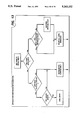
- FIG. 7 is a flow chart illustrating verification of NVM and PWB seals during booting
- FIG. 8 consisting of 8A and 8B are flow charts illustrating the process for identifying boot disk and loading preliminary booting software during booting
- FIG. 9 is a flow chart illustrating the low level software booting process
- FIG. 10 is a flow chart illustrating disk system initialization during booting
- FIG. 11 is a flow chart illustrating file system initialization during booting
- FIGS. 12 and 13 are flow charts illustrating application software initialization during booting
- FIG. 14 is a view depicting the "Physical Root Page" stored in disk memory
- FIG. 15 is a flow diagram illustrating selected steps of a claimed embodiment of the present invention.
- image input section 4 has both remote and on-site image inputs, enabling system 2 to provide network, scan, and print services.
- Other system combinations may be envisioned such as a stand alone printing system with on-site image input (i.e., a scanner), controller, and printer; a network printing system with remote input, controller, and printer; etc.
- printer section 8 may instead use a different printer type such as ink jet, ionographic, thermal, photographic, etc., and furthermore may be incorporated in electronic display systems, such as CRTs, LCDs, LEDs, etc. or else other image scanning/processing/recording systems, or else other signal transmitting/receiving, recording systems, etc. as well.
- printer section 8 may instead use a different printer type such as ink jet, ionographic, thermal, photographic, etc., and furthermore may be incorporated in electronic display systems, such as CRTs, LCDs, LEDs, etc. or else other image scanning/processing/recording systems, or else other signal transmitting/receiving, recording systems, etc. as well.
- printing system 2 A more detailed description of printing system 2 may be found in copending U.S. patent application Ser. No. 07/620,519, filed Nov. 30, 1990, to James R. Graves et al, and entitled “System For Scanning Signature Pages", the disclosure of which is incorporated by reference herein.
- controller section 7 is, for explanation purposes, divided into an image input controller 50, User Interface (UI) 52, system controller 54, disk memory 56, image manipulation section 58, Resource Manager 57, Diagnostic Manager 59, and image output controller 60.
- UI User Interface
- system controller 54 disk memory 56
- image manipulation section 58 image manipulation section 58
- Resource Manager 57 Resource Manager 57
- Diagnostic Manager 59 Diagnostic Manager 59
- image output controller 60 image output controller 60.
- UI 52 includes a combined operator controller/CRT display consisting of an interactive touchscreen 62, keyboard 64, and mouse 66.
- UI 52 interfaces the operator with printing system 2, enabling the operator to program print jobs and other instructions, to obtain system operating information, visual document facsimile display, programming information and icons, diagnostic information and pictorial views, etc.
- Items displayed on touchscreen 62 such as files and icons are actuated by either touching the displayed item on screen 62 with a finger or by using mouse 66 to point a cursor to the item selected and keying the mouse.
- the scanned image data input from scanner section 6 to controller section 7 is compressed by image compressor/processor 51 of image input controller 50 on PWB 70-3.
- the compressed image data with related image descriptors are placed in image files and temporarily stored in system memory 61 pending transfer to external memory 56 where the data is held pending use.
- the data in memory 56 When the compressed image data in memory 56 requires further processing or is required for display on touchscreen 62 of UI 52, or is required by printer section 8, the data is accessed in memory 56 and transferred to system memory 61. Where further processing other than that provided by processor 25 is required, the data is transferred to image manipulation section 58 on PWB 70-6 where additional processing steps such as collation, make ready (document editing), decomposition, rotation, etc. are carried out. Following processing, the data may be returned to external memory 56, sent to UI 52 for display on touchscreen 62, or sent to image output controller 60.
- Resource Manager 57 controls access to disks 90-1, 90-2, 90-3 and RAM 61 files while diagnostic manager 59 handles system faults.
- Image data output to image output controller 60 is decompressed and readied for printing and output to printer section 8.
- Image data sent to printer section 8 for printing is normally purged from memory 56 to make room for new image data.
- controller section 7 includes a plurality of Printed Wiring Boards (PWBs) 70, PWBs 70 being coupled with one another and with System Memory 61 by a pair of memory buses 72, 74.
- Memory controller 76 couples System Memory 61 with buses 72, 74.
- PWBs 70 include system processor PWB 70-1 having plural application or system processors 78; low speed I/O processor PWB 70-2 having UI communication controller 80 for transmitting data to and from UI 52, Boot Control and LSIO Services Processor 73, and Boot Bus Processor 75; PWBs 70-3, 70-4, 70-5 having disk drive controller/processors 82 with disk drives 83 for transmitting data to and from disks 90-1, 90-2, 90-3 respectively of external memory 56 (image compressor/processor 51 for compressing the image data and another application processor 78 are on PWB 70-3); image manipulation PWB 70-6 with image manipulation processors of image manipulation section 58; image generation processor PWBs 70-7, 70-8 with image generation processors 86 for processing the image data for printing by printer section 8; dispatch processor PWB 70-9 having dispatch processors 88, 89 for controlling transmission of data to and from printer section 8; and boot control-arbitration-scheduler PWB 70-10 having Channel Loader/Scheduler Processor
- Channels 81 are independent processors for handling the applications software, or input/output processors for handling peripheral devices such as disk drives.
- disk drives 83 there are disk channels used to interface disk drives 83 for disks 90-1, 90-2, 90-3, scanner interface channel, printer interface channel, etc.
- Memory 56 has plural hard disks 90-1, 90-2, 90-3 on which image files and system files are stored.
- Image files are typically files of scanned image data while system files comprise system operating files such as boot files, software files, data files, etc.
- System memory 61 which comprises a Random Access Memory or RAM, serves as a temporary store for data required during system operations.
- Memory 61 stores bits of data which can be written to (Data Entered) or read from (Data Used) from the memory. Other data in memory 61 is used for reference and remains loaded as long as power is supplied. Since memory 61 is volatile, that is, all data is lost when power to memory 61 is terminated, Non Volatile Memory or NVM, which essentially comprise RAM memory with backup battery 71 to supply DC voltage when power is turned off, are provided at several locations in the system as, for example, NVM 63 on Low Speed I/O Processor PWB 70-2 (FIG. 3B).
- System memory includes a battery date code identifying the date on which battery 71 was made. NVM 63 is used to store file management updates and file content updates.
- Image files are stored in Super Disk fashion as more fully described in copending U.S. patent application Ser. No. 07/590,634, filed Sep. 28, 1990 now abandoned and refiled under file wrapper continuation on Oct. 15, 1992 with Ser. No. 07/962,166, to George L. Eldridge, and entitled "Method of Operating Disk Drives in Parallel", the disclosure of which is incorporated by reference herein.
- image files are divided into sectors, each sector being a preset number of bytes. The sectors are written in succession to successive disks until all of the sectors that comprise the image file are stored.
- Super Disk allows faster read/write access to image files since all disks 90-1, 90-2, 90-3 can be accessed simultaneously. The risk incurred in this type of arrangement, however, is the loss of parts of a file should one or more of the disks fail which effectively results in loss of the entire file.
- a boot file 143 is replicated on each of the disks 90-1, 90-2, 90-3 for booting system 2.
- the boot software loads the necessary files from whichever disk 90-1, 90-2, or 90-3 is selected as the boot disk into memory and enables execution of the software. Since the boot file is replicated on all disks 90-1, 90-2, 90-3, any disk can be selected as the boot disk. In the subsequent explanation, disk 90-2 is presumed to be the boot disk.
- Warm Boot it is necessary to boot the system when power is first switched on (Cold Boot initiated) or when necessary during system operation (Warm Boot initiated).
- a manual ⁇ Boot ⁇ button (not shown) is provided for initiating a Warm Boot.
- Boot Bus 92 is coupled to Boot and LSIO service processor 73 and UI communication controller 80 on PWB 70-2 through boot bus processor 75, and to channel Loader/Scheduler processor 76 on PWB 70-10 through boot bus processor 77.
- the reset lines release processors 76 and 73 and UI communication controller 80, allowing Boot Bus 92 during the boot sequence to transmit software programs from PWB 70-2 to processor 76 on PWB 70-10 for downloading to each processor channel 81.
- Boot Channel 93 initializes all channels 81 to enable downloading of the micro code instructions by channel Loader/Scheduler processor 76 as described in TABLE I.
- processor identification seals 160 which comprise, for example, a 12 byte quantity having a 6 byte time stamp 162 (read from the system real time clock 84 shown in FIG. 3B) and a 6 byte processor identifier (PROC ID) 164, are provided.
- the PROC ID 164 is kept in a memory chip such as PROM 69 socketed onto PWB 70-2 (seen in FIG. 3B) and remains with the machine in the event PWB 70-2 is replaced.
- a copy of the processor ID and initialized time stamp (SysNVM Seal) is stored in system NVM 63 on PWB 70-2 (seen in FIG. 3B).
- the disk Physical Volume Root Page 85 PV Root Page seen in FIGS. 4 and 14
- the NVM 63 and PWB 70-2 seals are verified by reading and comparing the PROC ID 164 stored in PROM 69 with the PROC ID from the SysNVM Seal. If not the same, PWB 70-2 is defective or replaced. Also an NVM retention check is run to see if NVM 63 held its data while power to the system was off and the data code for backup battery 71 checked to see if battery 71 is fresh.
- the PROC ID is compared with the PVRoot Page PROC ID to see if the boot disk has been replaced and the SysNVM Seal is compared with the PVRoot Page Seals on the other disks to see any of the other disks have been replaced.
- a difference between the disk position in the PVRootPage and the current location of a disk indicates that two disks have been swapped, and are therefore not in correct position in the disk memory.
- the disk system file system, and application software are initialized to complete the booting process.
- the disk number is incremented by Scheduler/Processor 76 (seen in FIG. 3A) and the booting process started over using a second disk, i.e., either disk 90-1 or 90-3. If the second disk is found to be unavailable, booting from the third disk is tried. Where booting cannot be made from any disk following a preset number of tries, the system returns to a service dialogue routine in Diagnostic Manager 59 (seen in FIG. 2), requiring servicing by the Tech Rep and booting of the system from an outside source such as streaming tape.
- the defective PWB 70-2 is removed and a new PWB installed.
- PROM 69 on the defective PWB is removed and reinstalled on the new PWB to preserve identity between the new PWB and printing system 2.
- a special PWB installation control in which software determines the current state of the system (TABLE II) and based on that, performs specific initialization steps (TABLE V). For this, the software reads the PV Root Page Seals from each disk 90-1, 90-2, 90-3 and the SysNVM Seal from the new NVM and compares these with the PROC ID embedded in PROM 69. Depending on the result, a Message Number (TABLE II) is generated which, as shown in TABLE III, provides a Diagnostic Message with information for the Tech Rep. Additionally, a specific fault code (Fault Code) may be identified with further instructions to the Tech Rep (TABLE III).
- Fault Code fault code
- the system initializing steps described in TABLE V are taken to initialize the system.
- the System State was determined to be 4 which as seen in TABLE II, requires steps a, b, c, and d as the Initialize Action.
- the new PWB is initialized by setting up default hardware configuration values in the NVM (step a), setting the NVM initialized flag to TRUE (step b), generating the PROC ID Seal for the new NVM (step c), and copying the NVM seal to disks 90-1, 90-2, 90-3 (step d).
- the present invention protects the integrity of the combination of disk updates resident in NVM and the disk contents by preventing disk updates from occurring if the NVM or drives have been replaced. Additionally, the present invention provides confirmation to the Tech Rep that the elements maintained under the seal have been replaced.
- Channel processors 81 perform reads and writes to various sections of memory 61.
- Disk controller microcode is downloaded to disk controller processors 82 via boot bus 92 and boot download control logic 79.
- Channel loader microcode is sent via boot bus 92 to PWB 70-10. Microcode is then downloaded using boot download control logic 79 to channel loader/scheduler processor 76.
- Channel loader/scheduler processor 76 requests that disk controller processor 82 retrieve the controller microcode file from disk 90-2. Disk controller processor 82 ships file to memory 61. Channel loader/scheduler processor 76 then downloads microcode to each channel 81 using boot download control logic.
- Channel loader/scheduler processor 76 requests that disk controller processor 83 retrieve the application software loader program from disk 90-2. Disk controller processor 83 ships file to memory 61.
- Scheduler microcode is downloaded into channel loader/scheduler processor 76.
- Processor 76 will now perform only as a scheduler processor.
- Application software loader program is started. Application software is retrieved from disk 90-2 and stored in memory 61.
Abstract
Description
                                  TABLE II
__________________________________________________________________________
System
    Prom
        Bd Disks
               Message
                    Fault
                        Initialize
State
    Repl
        Repl
           Repl
               Number
                    Code
                        Action
                             Means of Identifying Items
__________________________________________________________________________
                             Replaced
0   N   N  0   2        a,b,c,d
                             Pid = NvmPid, NvmSeal = [all] DiskSeals
1   x   x  x   4    FC01
                        No Op
                             Pid has bad checksum or checksum compliment
2   N   N  1 or 2
               3    FC02
                        a,b,c,d
                             Pid = NvmPid, NvmSeal = [1 or 2] DiskSeals
3   N   N  3   3    FC03
                        a,b,c,d
                             Pid = NvmPid, NvmSeal = [no] DiskSeals
                             [all] DiskSeals are consistent with each
                             other
4   N   Y  0   1        a,b,c,d
                             Pid ≠ NvmPid, Pid = [all] DiskPids,
                             NvmSeal = [no] DiskSeals,
                             [all] DiskSeals are consistent with each
                             other
5   N   Y  1 or 2
               1        a,b,c,d
                             Pid ≠ NvmPid, Pid = [1 or
                             2] DiskPids,
                             NvmSeal = [no] DiskSeals
6   N   Y  3   3    FC04
                        a,b,c
                             Pid ≠ NvmPid, NvmSeal
                             = [no] DiskSeals
7   Y   N  0   1        c,d  Pid ≠ NvmPid, NvmSeal
                             = [all] DiskSeals
8   Y   N  1 or 2
               1        c,d  Pid ≠ NvmPid, NvmSeal = [1 or 2]
                             DiskSeals
9   Y   N  3   3    FC04
                        a,b,c
                             Pid ≠ NvmPid, NvmSeal
                             = [no] DiskSeals
10  Y   Y  0   3    FC05
                        a,b,c,d
                             Pid ≠ NvmPid, NvmSeal
                             = [no] DiskSeals
                             [all] DiskSeals are consistent
11  Y   Y  1 or 2
               3    FC04
                        a,b,c
                             Pid ≠ NvmPid, NvmSeal
                             = [no] DiskSeals
12  Y   Y  3   3    FC04
                        a,b,c
                             Pid ≠ NvmPid, NvmSeal
                             = [no] DiskSeals
13  Y   Y  0   3    FC03
                        a,b,c,d
                             Pid = NvmPid, NvmSeal = [no] DiskSeals
                             [all] DiskSeals are consistent with each
                             other
14  N   N  3   3    FC04
                        a,b,c
                             Pid = NvmPid, NvmSeal = [no] DiskSeals
                             [1 or 2] DiskSeals are inconsistent
__________________________________________________________________________
 Note:
 1. If a disk seal cannot be read, it is considered not to match any other
 seal, and the disk is treated as if it had been replaced.
 2. If all disks have been replaced, then the system will not be able to
 disk boot. The Service Rep must Stream Tape Boot.
 3. Cases 6,9,11, and 12 are indistinguishable to the software, so it is
 Unknown what the Service Rep did.
 4. Cases 3 and 13 are indistinguishable to the software, so it is Unknown
 what the Service Rep did.
TABLE III ______________________________________ Fault Code Instruction to ServiceRep ______________________________________ FC01 1. Check to see that Proc Id PROM is correctly installed on bd. 2. Replace board 70-2. 3. ReplaceProc Id PROM 69. FC02 It is not necessary to Install the pwb 70-2 if only disks have been replaced. FC03 If the pwb 70-2 was replaced, be certain that the machine's original Proc Id PROM was inserted in the new board. FC04 After finishing board installation, Stream Tape Boot is mandatory. FC05 Be certain that the machine's original Proc Id PROM was inserted in the new board 70-2. ______________________________________
              TABLE IV
______________________________________
                            Message
Diagnostic Message          Number
______________________________________
PWB 70-2 installation confirmed. Press Yes to
                            1
continue.
New PWB not detected. Press Yes to continue.
                            2
PWB and/or disk replacement detected -- see Fault
                            3
Code for additional activities required.
Failure detected during installation -- see Fault
                            4
Code.
______________________________________
              TABLE V
______________________________________
Initialize Action, Performed by PLM
______________________________________
a   Set up default hardware configuration values in PLM NVM.
b   Set NVM initialized flag to TRUE.
c   Generate Seal, copy it to NVM, read back and verify.
d   Copy NVM seal to UNREPLACED disks, read back and
    verify.
______________________________________
Claims (10)
Priority Applications (2)
| Application Number | Priority Date | Filing Date | Title |
|---|---|---|---|
| US07/678,922 US5263152A (en) | 1991-04-01 | 1991-04-01 | Process for replacing non-volatile memory in electronic printing systems |
| JP3246342A JPH0814802B2 (en) | 1991-04-01 | 1991-09-26 | Method of replacing non-volatile memory in an electronic printing system |
Applications Claiming Priority (1)
| Application Number | Priority Date | Filing Date | Title |
|---|---|---|---|
| US07/678,922 US5263152A (en) | 1991-04-01 | 1991-04-01 | Process for replacing non-volatile memory in electronic printing systems |
Publications (1)
| Publication Number | Publication Date |
|---|---|
| US5263152A true US5263152A (en) | 1993-11-16 |
Family
ID=24724872
Family Applications (1)
| Application Number | Title | Priority Date | Filing Date |
|---|---|---|---|
| US07/678,922 Expired - Fee Related US5263152A (en) | 1991-04-01 | 1991-04-01 | Process for replacing non-volatile memory in electronic printing systems |
Country Status (2)
| Country | Link |
|---|---|
| US (1) | US5263152A (en) |
| JP (1) | JPH0814802B2 (en) |
Cited By (12)
| Publication number | Priority date | Publication date | Assignee | Title |
|---|---|---|---|---|
| US5471631A (en) * | 1992-10-19 | 1995-11-28 | International Business Machines Corporation | Using time stamps to correlate data processing event times in connected data processing units |
| US5493649A (en) * | 1994-06-21 | 1996-02-20 | Microsoft Corporation | Detecting corruption in a computer program at execution time using a checksum |
| US5537218A (en) * | 1991-06-27 | 1996-07-16 | Canon Kabushiki Kaisha | Facsimile apparatus |
| US5644618A (en) * | 1991-05-31 | 1997-07-01 | Nec Corporation | Method of self-diagnosing a mobile telephone set for use in a mobile telephone switching system and a mobile telephone set to which the method is applied |
| US5712969A (en) * | 1993-09-24 | 1998-01-27 | Robert Bosch Gmbh | Method for completely reprogramming an erasable, non-volatile memory |
| US5758103A (en) * | 1995-08-31 | 1998-05-26 | Samsung Electronics Co., Ltd. | Circuit for replacing a peripheral device of a computer system and method therefor |
| US5819020A (en) * | 1995-10-16 | 1998-10-06 | Network Specialists, Inc. | Real time backup system |
| US6029238A (en) * | 1994-03-31 | 2000-02-22 | Canon Kabushiki Kaisha | Control of information processing using one or more peripheral apparatus |
| US20020024682A1 (en) * | 2000-01-20 | 2002-02-28 | Woo-Hwa Ha | Method of storing initial use date of printer and informing the date |
| US6565443B1 (en) | 1999-09-14 | 2003-05-20 | Innovative Gaming Corporation | System and method for verifying the contents of a mass storage device before granting access to computer readable data stored on the device |
| US20120314243A1 (en) * | 2011-06-07 | 2012-12-13 | Canon Kabushiki Kaisha | Electronic device with backed-up memory, and control method and storage medium therefor |
| US20190294360A1 (en) * | 2017-01-17 | 2019-09-26 | Fujitsu Client Computing Limited | Information processing apparatus and computer-readable recording medium |
Citations (1)
| Publication number | Priority date | Publication date | Assignee | Title |
|---|---|---|---|---|
| US4499581A (en) * | 1982-09-21 | 1985-02-12 | Xerox Corporation | Self testing system for reproduction machine |
Family Cites Families (3)
| Publication number | Priority date | Publication date | Assignee | Title |
|---|---|---|---|---|
| JPS63189938A (en) * | 1987-02-02 | 1988-08-05 | Nec Corp | Checking system for the number of versions in information processing system |
| JPS63285634A (en) * | 1987-05-19 | 1988-11-22 | Nec Corp | Information processor |
| JPH02191031A (en) * | 1989-01-20 | 1990-07-26 | Ricoh Co Ltd | Information processor |
-
1991
- 1991-04-01 US US07/678,922 patent/US5263152A/en not_active Expired - Fee Related
- 1991-09-26 JP JP3246342A patent/JPH0814802B2/en not_active Expired - Fee Related
Patent Citations (1)
| Publication number | Priority date | Publication date | Assignee | Title |
|---|---|---|---|---|
| US4499581A (en) * | 1982-09-21 | 1985-02-12 | Xerox Corporation | Self testing system for reproduction machine |
Cited By (16)
| Publication number | Priority date | Publication date | Assignee | Title |
|---|---|---|---|---|
| US5644618A (en) * | 1991-05-31 | 1997-07-01 | Nec Corporation | Method of self-diagnosing a mobile telephone set for use in a mobile telephone switching system and a mobile telephone set to which the method is applied |
| US5537218A (en) * | 1991-06-27 | 1996-07-16 | Canon Kabushiki Kaisha | Facsimile apparatus |
| US5471631A (en) * | 1992-10-19 | 1995-11-28 | International Business Machines Corporation | Using time stamps to correlate data processing event times in connected data processing units |
| US5712969A (en) * | 1993-09-24 | 1998-01-27 | Robert Bosch Gmbh | Method for completely reprogramming an erasable, non-volatile memory |
| US6029238A (en) * | 1994-03-31 | 2000-02-22 | Canon Kabushiki Kaisha | Control of information processing using one or more peripheral apparatus |
| US5493649A (en) * | 1994-06-21 | 1996-02-20 | Microsoft Corporation | Detecting corruption in a computer program at execution time using a checksum |
| US5758103A (en) * | 1995-08-31 | 1998-05-26 | Samsung Electronics Co., Ltd. | Circuit for replacing a peripheral device of a computer system and method therefor |
| US5819020A (en) * | 1995-10-16 | 1998-10-06 | Network Specialists, Inc. | Real time backup system |
| US5974563A (en) * | 1995-10-16 | 1999-10-26 | Network Specialists, Inc. | Real time backup system |
| US6565443B1 (en) | 1999-09-14 | 2003-05-20 | Innovative Gaming Corporation | System and method for verifying the contents of a mass storage device before granting access to computer readable data stored on the device |
| US20020024682A1 (en) * | 2000-01-20 | 2002-02-28 | Woo-Hwa Ha | Method of storing initial use date of printer and informing the date |
| US7193737B2 (en) | 2000-01-20 | 2007-03-20 | Samsung Electronics Co., Ltd. | Method of storing initial use date of printer and informing the date |
| US20120314243A1 (en) * | 2011-06-07 | 2012-12-13 | Canon Kabushiki Kaisha | Electronic device with backed-up memory, and control method and storage medium therefor |
| US8760701B2 (en) * | 2011-06-07 | 2014-06-24 | Canon Kabushiki Kaisha | Electronic device with backed-up memory, and control method and storage medium therefor |
| US20190294360A1 (en) * | 2017-01-17 | 2019-09-26 | Fujitsu Client Computing Limited | Information processing apparatus and computer-readable recording medium |
| US10942669B2 (en) * | 2017-01-17 | 2021-03-09 | Fujitsu Client Computing Limited | Information processing apparatus and computer-readable recording medium |
Also Published As
| Publication number | Publication date |
|---|---|
| JPH04320544A (en) | 1992-11-11 |
| JPH0814802B2 (en) | 1996-02-14 |
Similar Documents
| Publication | Publication Date | Title |
|---|---|---|
| US5257377A (en) | Process for automatically migrating a subset of updated files from the boot disk to the replicated disks | |
| US5241672A (en) | System using the storage level of file updates in nonvolatile memory to trigger saving of RAM to disk and using the file updates to reboot after crash | |
| US5590306A (en) | Memory card management system for writing data with usage and recording codes made significant | |
| US6212600B1 (en) | Method and apparatus for sanitization of fixed storage devices | |
| US5357607A (en) | File storage process for electronic printing systems having multiple disks | |
| KR100348007B1 (en) | Method and apparatus for restoration of a computer system hard drive | |
| JP4404940B2 (en) | Method and system for providing custom software images to a computer system | |
| US6308265B1 (en) | Protection of boot block code while allowing write accesses to the boot block | |
| US7337309B2 (en) | Secure online BIOS update schemes | |
| US5263152A (en) | Process for replacing non-volatile memory in electronic printing systems | |
| US5212786A (en) | File compaction process for electronic printing systems | |
| US7313682B2 (en) | Method and system for updating boot memory that stores a fail-safe reset code and is configured to store boot code and boot updater code | |
| US7007195B2 (en) | BIOS shadowed small-print hard disk drive as robust, always on, backup for hard disk image & software failure | |
| US6609152B1 (en) | System for avoiding the assignment of duplicate MAC addresses to network interface devices | |
| US20030075599A1 (en) | Personal work environment setting method | |
| US5249288A (en) | Process for accommodating bad disk pages in an electronic printing system | |
| JPH113223A (en) | Information processor and information storage method | |
| US5345581A (en) | Process for replacing storage media in electronic printing systems | |
| JPH09101887A (en) | Disk array device | |
| JP2020004134A (en) | Image forming device, method of controlling image forming device, and program | |
| JP3453582B2 (en) | Disk array device firmware management system and management method therefor | |
| JP2000322333A (en) | Automatic saving/automatic restoration system and method for information specific to computer system | |
| JP2019207699A (en) | Information processing device and control method therefor | |
| KR20060120988A (en) | Apparatus and method for system booting which uses redundancy mechanism boot rom | |
| JPH076071A (en) | Device and method for information management |
Legal Events
| Date | Code | Title | Description |
|---|---|---|---|
| AS | Assignment |
Owner name: XEROX CORPORATION, STAMFORD, COUNTY OF FAIRFIELD, Free format text: ASSIGNMENT OF ASSIGNORS INTEREST.;ASSIGNORS:SMITH, MARK A.;SATHI, KITTY;LATONE, JACK T.;REEL/FRAME:005664/0084 Effective date: 19910326 |
|
| FEPP | Fee payment procedure |
Free format text: PAYOR NUMBER ASSIGNED (ORIGINAL EVENT CODE: ASPN); ENTITY STATUS OF PATENT OWNER: LARGE ENTITY |
|
| FPAY | Fee payment |
Year of fee payment: 4 |
|
| FPAY | Fee payment |
Year of fee payment: 8 |
|
| AS | Assignment |
Owner name: BANK ONE, NA, AS ADMINISTRATIVE AGENT, ILLINOIS Free format text: SECURITY INTEREST;ASSIGNOR:XEROX CORPORATION;REEL/FRAME:013153/0001 Effective date: 20020621 |
|
| AS | Assignment |
Owner name: JPMORGAN CHASE BANK, AS COLLATERAL AGENT, TEXAS Free format text: SECURITY AGREEMENT;ASSIGNOR:XEROX CORPORATION;REEL/FRAME:015134/0476 Effective date: 20030625 Owner name: JPMORGAN CHASE BANK, AS COLLATERAL AGENT,TEXAS Free format text: SECURITY AGREEMENT;ASSIGNOR:XEROX CORPORATION;REEL/FRAME:015134/0476 Effective date: 20030625 |
|
| REMI | Maintenance fee reminder mailed | ||
| LAPS | Lapse for failure to pay maintenance fees | ||
| STCH | Information on status: patent discontinuation |
Free format text: PATENT EXPIRED DUE TO NONPAYMENT OF MAINTENANCE FEES UNDER 37 CFR 1.362 |
|
| FP | Lapsed due to failure to pay maintenance fee |
Effective date: 20051116 |
|
| AS | Assignment |
Owner name: XEROX CORPORATION, CONNECTICUT Free format text: RELEASE BY SECURED PARTY;ASSIGNOR:JPMORGAN CHASE BANK, N.A. AS SUCCESSOR-IN-INTEREST ADMINISTRATIVE AGENT AND COLLATERAL AGENT TO JPMORGAN CHASE BANK;REEL/FRAME:066728/0193 Effective date: 20220822 |