US5266801A - Jumping probe microscope - Google Patents
Jumping probe microscope Download PDFInfo
- Publication number
- US5266801A US5266801A US08/009,076 US907693A US5266801A US 5266801 A US5266801 A US 5266801A US 907693 A US907693 A US 907693A US 5266801 A US5266801 A US 5266801A
- Authority
- US
- United States
- Prior art keywords
- sample
- probe
- tip
- atomic force
- scanning
- Prior art date
- Legal status (The legal status is an assumption and is not a legal conclusion. Google has not performed a legal analysis and makes no representation as to the accuracy of the status listed.)
- Expired - Lifetime
Links
- 239000000523 sample Substances 0.000 title claims abstract description 241
- 230000009191 jumping Effects 0.000 title description 7
- 230000033001 locomotion Effects 0.000 claims abstract description 32
- 238000005452 bending Methods 0.000 claims description 28
- 230000005291 magnetic effect Effects 0.000 claims description 7
- 238000000034 method Methods 0.000 claims description 7
- 230000004044 response Effects 0.000 claims description 6
- 230000000704 physical effect Effects 0.000 claims description 5
- 230000006872 improvement Effects 0.000 claims description 2
- 239000003302 ferromagnetic material Substances 0.000 claims 4
- 230000005641 tunneling Effects 0.000 abstract description 54
- 230000010355 oscillation Effects 0.000 description 10
- 238000012876 topography Methods 0.000 description 8
- 238000010586 diagram Methods 0.000 description 6
- 230000008901 benefit Effects 0.000 description 5
- 230000003466 anti-cipated effect Effects 0.000 description 4
- 230000000630 rising effect Effects 0.000 description 4
- 238000005070 sampling Methods 0.000 description 4
- 238000013459 approach Methods 0.000 description 3
- 230000003247 decreasing effect Effects 0.000 description 3
- 238000001914 filtration Methods 0.000 description 3
- 230000008859 change Effects 0.000 description 2
- 230000006870 function Effects 0.000 description 2
- 230000008569 process Effects 0.000 description 2
- 235000008694 Humulus lupulus Nutrition 0.000 description 1
- 230000001680 brushing effect Effects 0.000 description 1
- 238000012937 correction Methods 0.000 description 1
- 238000013480 data collection Methods 0.000 description 1
- 238000013500 data storage Methods 0.000 description 1
- 238000011161 development Methods 0.000 description 1
- 239000012777 electrically insulating material Substances 0.000 description 1
- 230000005294 ferromagnetic effect Effects 0.000 description 1
- 230000010354 integration Effects 0.000 description 1
- 238000005259 measurement Methods 0.000 description 1
- 230000003287 optical effect Effects 0.000 description 1
- 238000004574 scanning tunneling microscopy Methods 0.000 description 1
- 230000035945 sensitivity Effects 0.000 description 1
- 238000012360 testing method Methods 0.000 description 1
Images


Classifications
-
- G—PHYSICS
- G01—MEASURING; TESTING
- G01Q—SCANNING-PROBE TECHNIQUES OR APPARATUS; APPLICATIONS OF SCANNING-PROBE TECHNIQUES, e.g. SCANNING PROBE MICROSCOPY [SPM]
- G01Q20/00—Monitoring the movement or position of the probe
- G01Q20/04—Self-detecting probes, i.e. wherein the probe itself generates a signal representative of its position, e.g. piezoelectric gauge
-
- B—PERFORMING OPERATIONS; TRANSPORTING
- B82—NANOTECHNOLOGY
- B82Y—SPECIFIC USES OR APPLICATIONS OF NANOSTRUCTURES; MEASUREMENT OR ANALYSIS OF NANOSTRUCTURES; MANUFACTURE OR TREATMENT OF NANOSTRUCTURES
- B82Y35/00—Methods or apparatus for measurement or analysis of nanostructures
-
- G—PHYSICS
- G01—MEASURING; TESTING
- G01Q—SCANNING-PROBE TECHNIQUES OR APPARATUS; APPLICATIONS OF SCANNING-PROBE TECHNIQUES, e.g. SCANNING PROBE MICROSCOPY [SPM]
- G01Q20/00—Monitoring the movement or position of the probe
- G01Q20/02—Monitoring the movement or position of the probe by optical means
-
- G—PHYSICS
- G01—MEASURING; TESTING
- G01Q—SCANNING-PROBE TECHNIQUES OR APPARATUS; APPLICATIONS OF SCANNING-PROBE TECHNIQUES, e.g. SCANNING PROBE MICROSCOPY [SPM]
- G01Q60/00—Particular types of SPM [Scanning Probe Microscopy] or microscopes; Essential components thereof
- G01Q60/10—STM [Scanning Tunnelling Microscopy] or apparatus therefor, e.g. STM probes
- G01Q60/16—Probes, their manufacture, or their related instrumentation, e.g. holders
-
- G—PHYSICS
- G01—MEASURING; TESTING
- G01Q—SCANNING-PROBE TECHNIQUES OR APPARATUS; APPLICATIONS OF SCANNING-PROBE TECHNIQUES, e.g. SCANNING PROBE MICROSCOPY [SPM]
- G01Q60/00—Particular types of SPM [Scanning Probe Microscopy] or microscopes; Essential components thereof
- G01Q60/24—AFM [Atomic Force Microscopy] or apparatus therefor, e.g. AFM probes
- G01Q60/32—AC mode
- G01Q60/34—Tapping mode
-
- Y—GENERAL TAGGING OF NEW TECHNOLOGICAL DEVELOPMENTS; GENERAL TAGGING OF CROSS-SECTIONAL TECHNOLOGIES SPANNING OVER SEVERAL SECTIONS OF THE IPC; TECHNICAL SUBJECTS COVERED BY FORMER USPC CROSS-REFERENCE ART COLLECTIONS [XRACs] AND DIGESTS
- Y10—TECHNICAL SUBJECTS COVERED BY FORMER USPC
- Y10S—TECHNICAL SUBJECTS COVERED BY FORMER USPC CROSS-REFERENCE ART COLLECTIONS [XRACs] AND DIGESTS
- Y10S977/00—Nanotechnology
- Y10S977/84—Manufacture, treatment, or detection of nanostructure
- Y10S977/849—Manufacture, treatment, or detection of nanostructure with scanning probe
- Y10S977/85—Scanning probe control process
- Y10S977/851—Particular movement or positioning of scanning tip
-
- Y—GENERAL TAGGING OF NEW TECHNOLOGICAL DEVELOPMENTS; GENERAL TAGGING OF CROSS-SECTIONAL TECHNOLOGIES SPANNING OVER SEVERAL SECTIONS OF THE IPC; TECHNICAL SUBJECTS COVERED BY FORMER USPC CROSS-REFERENCE ART COLLECTIONS [XRACs] AND DIGESTS
- Y10—TECHNICAL SUBJECTS COVERED BY FORMER USPC
- Y10S—TECHNICAL SUBJECTS COVERED BY FORMER USPC CROSS-REFERENCE ART COLLECTIONS [XRACs] AND DIGESTS
- Y10S977/00—Nanotechnology
- Y10S977/84—Manufacture, treatment, or detection of nanostructure
- Y10S977/849—Manufacture, treatment, or detection of nanostructure with scanning probe
- Y10S977/86—Scanning probe structure
- Y10S977/861—Scanning tunneling probe
-
- Y—GENERAL TAGGING OF NEW TECHNOLOGICAL DEVELOPMENTS; GENERAL TAGGING OF CROSS-SECTIONAL TECHNOLOGIES SPANNING OVER SEVERAL SECTIONS OF THE IPC; TECHNICAL SUBJECTS COVERED BY FORMER USPC CROSS-REFERENCE ART COLLECTIONS [XRACs] AND DIGESTS
- Y10—TECHNICAL SUBJECTS COVERED BY FORMER USPC
- Y10S—TECHNICAL SUBJECTS COVERED BY FORMER USPC CROSS-REFERENCE ART COLLECTIONS [XRACs] AND DIGESTS
- Y10S977/00—Nanotechnology
- Y10S977/84—Manufacture, treatment, or detection of nanostructure
- Y10S977/849—Manufacture, treatment, or detection of nanostructure with scanning probe
- Y10S977/86—Scanning probe structure
- Y10S977/862—Near-field probe
-
- Y—GENERAL TAGGING OF NEW TECHNOLOGICAL DEVELOPMENTS; GENERAL TAGGING OF CROSS-SECTIONAL TECHNOLOGIES SPANNING OVER SEVERAL SECTIONS OF THE IPC; TECHNICAL SUBJECTS COVERED BY FORMER USPC CROSS-REFERENCE ART COLLECTIONS [XRACs] AND DIGESTS
- Y10—TECHNICAL SUBJECTS COVERED BY FORMER USPC
- Y10S—TECHNICAL SUBJECTS COVERED BY FORMER USPC CROSS-REFERENCE ART COLLECTIONS [XRACs] AND DIGESTS
- Y10S977/00—Nanotechnology
- Y10S977/84—Manufacture, treatment, or detection of nanostructure
- Y10S977/849—Manufacture, treatment, or detection of nanostructure with scanning probe
- Y10S977/86—Scanning probe structure
- Y10S977/863—Atomic force probe
-
- Y—GENERAL TAGGING OF NEW TECHNOLOGICAL DEVELOPMENTS; GENERAL TAGGING OF CROSS-SECTIONAL TECHNOLOGIES SPANNING OVER SEVERAL SECTIONS OF THE IPC; TECHNICAL SUBJECTS COVERED BY FORMER USPC CROSS-REFERENCE ART COLLECTIONS [XRACs] AND DIGESTS
- Y10—TECHNICAL SUBJECTS COVERED BY FORMER USPC
- Y10S—TECHNICAL SUBJECTS COVERED BY FORMER USPC CROSS-REFERENCE ART COLLECTIONS [XRACs] AND DIGESTS
- Y10S977/00—Nanotechnology
- Y10S977/84—Manufacture, treatment, or detection of nanostructure
- Y10S977/849—Manufacture, treatment, or detection of nanostructure with scanning probe
- Y10S977/86—Scanning probe structure
- Y10S977/868—Scanning probe structure with optical means
- Y10S977/869—Optical microscope
-
- Y—GENERAL TAGGING OF NEW TECHNOLOGICAL DEVELOPMENTS; GENERAL TAGGING OF CROSS-SECTIONAL TECHNOLOGIES SPANNING OVER SEVERAL SECTIONS OF THE IPC; TECHNICAL SUBJECTS COVERED BY FORMER USPC CROSS-REFERENCE ART COLLECTIONS [XRACs] AND DIGESTS
- Y10—TECHNICAL SUBJECTS COVERED BY FORMER USPC
- Y10S—TECHNICAL SUBJECTS COVERED BY FORMER USPC CROSS-REFERENCE ART COLLECTIONS [XRACs] AND DIGESTS
- Y10S977/00—Nanotechnology
- Y10S977/84—Manufacture, treatment, or detection of nanostructure
- Y10S977/849—Manufacture, treatment, or detection of nanostructure with scanning probe
- Y10S977/86—Scanning probe structure
- Y10S977/873—Tip holder
-
- Y—GENERAL TAGGING OF NEW TECHNOLOGICAL DEVELOPMENTS; GENERAL TAGGING OF CROSS-SECTIONAL TECHNOLOGIES SPANNING OVER SEVERAL SECTIONS OF THE IPC; TECHNICAL SUBJECTS COVERED BY FORMER USPC CROSS-REFERENCE ART COLLECTIONS [XRACs] AND DIGESTS
- Y10—TECHNICAL SUBJECTS COVERED BY FORMER USPC
- Y10S—TECHNICAL SUBJECTS COVERED BY FORMER USPC CROSS-REFERENCE ART COLLECTIONS [XRACs] AND DIGESTS
- Y10S977/00—Nanotechnology
- Y10S977/84—Manufacture, treatment, or detection of nanostructure
- Y10S977/849—Manufacture, treatment, or detection of nanostructure with scanning probe
- Y10S977/86—Scanning probe structure
- Y10S977/875—Scanning probe structure with tip detail
Definitions
- This invention relates to microscopes able to display a physical property of a surface and, more particularly, to a scanning probe microscope wherein a probe tip is moved over the surface of a sample in a raster scan comprising a series of transverse scans during which data reflecting the height of the surface is gathered at a plurality of data points to be used by controlling and calculating computer means to construct an image of the topography of the surface to scanning apparatus for increasing the speed of the scan comprising jump scanning means for moving the probe tip along each of the transverse scans in a series of jumps wherein the probe tip is moved from a position adjacent the surface to a height above the surface where there is virtually no possibility that the probe tip will strike the surface when the probe tip is moved horizontally and data gathering logic means included within the computer means for gathering the data at a pre-selected portion of selected ones of the jumps.
- Scanning probe microscopes are rapidly gaining popularity because of their ability to display surface features to an atomic level with what are, compared to other microscopes of such capability, simple and inexpensive devices.
- Typical of scanning probe microscopes are the Scanning Tunneling Microscope (STM) as described in U.S. Pat. No. 4,343,993 by Binning and Rohrer and the Atomic Force Microscope (AFM) as described in U.S. Pat. No. 4,724,318 by Binnig et al.
- a sharp metallic tip is maintained a few atomic diameters above the surface of a conducting surface while a tunneling current flows between the tip and the surface as the tip is scanned across the surface.
- the tip is scanned "across the sample surface at a tunneling distance while tunneling current flows between the tip and the sample surface.” Since the tunneling current flows only when the tip is within a few atomic diameters of the surface, the STM has the advantage of seeing atomic features on the surface; however, the disadvantage is that on large scans where atomic resolution is or no interest, the tip must still be a few atoms above the surface.
- the vertical positioning system cannot respond fast enough to keep the tip from hitting the surface, causing the tip to be worn away and also damaging the surface.
- the fastest scan velocity for an STM is 10 microns/second over a "rough" surface such as a stamper for making compact disks. At higher velocities the tip tends to be damaged.
- This scan rate is about 20,000 atoms per second and the feedback response to about 20 kHz.
- the feedback system corrects the vertical position of the tip for a horizontal motion of one atom, which is the rate required to keep the tip from running into ledges which are more than a few atoms high. Faster responding positioners and feedback loops would be needed for faster scans.
- an Atomic Force Microscope is another type of scanning probe microscope.
- This device has a sharp tip mounted on a lever and the tip is brought down into near contact, or contact, with the surface of the sample to be scanned.
- the force of contact is measured by the deflection of the lever, usually by a beam of light which is bounced off the lever.
- the tip With a feedback system moving the tip (or, alternatively, the sample) up and down to maintain constant force, the tip is scanned across the sample. If the force is kept small, the tip will not be damaged; but, on large scans the feedback system cannot responsed fast enough to keep the force small, so the scan rate becomes limited in order to not damage the tip.
- a scanning probe microscope wherein a probe tip is moved over the surface of a sample in a raster scan comprising a series of transverse scans during which data reflecting the height of the surface is gathered at a plurality of data points to be used by controlling and calculating computer means to construct an image of the topography of the surface
- the scanning apparatus of the present invention for increasing the speed of the scan comprising jump scanning means for moving the probe tip along each of the transverse scans in a series of jumps wherein the probe tip is moved from a position adjacent the surface to a height above the surface where there is little possibility that the probe tip will strike the surface when the probe tip is moved horizontally and data gathering logic means included within the computer means for gathering the data at a pre-selected portion of selected ones of the jumps.
- the jump scanning means comprises, means for lifting the probe tip from a position adjacent the surface to a height above the surface where there is little possibility that the probe tip will strike the surface when the probe tip is moved horizontally; means for moving the probe tip horizontally to a next position; and, means for lowering the probe tip from the raised position to a position adjacent the surface.
- the means for lifting the probe tip from a position adjacent the surface to a height above the surface is a high gain means and the means for lowering the probe tip from the raised position to a position adjacent the surface is a low gain means whereby the probe tip is lifted from the surface rapidly and lowered towards the surface slowly to avoid damage to the probe tip by striking the surface.
- the scanning probe microscope is a scanning tunneling microscope wherein the means for lowering the probe tip from the raised position to a position adjacent the surface comprises, means for lowering the probe tip towards the surface; means for sensing a tunneling current flowing between the probe tip and the surface before the probe tip touches the surface; and, means for stopping the lowering of the probe tip towards the surface when the tunneling current reaches a pre-established threshold amount.
- the means for stopping the lowering of the probe tip towards the surface when the tunneling current reaches a pre-established threshold amount comprises means for stopping the lowering of the probe tip towards the surface when the flow of a tunneling current is detected, wherein additionally the means for gathering the data at selected ones of the next positions includes means for adjusting data reflecting the height of the probe tip above the surface as a function of the amount of tunneling current flowing between the probe tip and the surface.
- the means for lowering the probe tip towards the surface comprises means for lowering the probe tip towards the surface at a first rate until a tunneling current is detected and means for continuing to lower the probe tip towards the surface at a second rate which is slower than the first rate, wherein the means for stopping the lowering of the probe tip towards the surface when the tunneling current reaches a pre-established threshold amount comprises means for stopping the lowering of the probe tip towards the surface when the tunneling current reaches a value placing the probe tip at a pre-established known constant height above the surface.
- a preferred addition for further increasing the speed of the scan comprises the means for lifting the probe tip from a position adjacent the surface to a height above the surface where there is little possibility that the probe tip will strike the surface when the probe tip is moved horizontally comprising means for saving data for preceding data points; means for at each point where the probe tip is to be lifted looking at the saved data for adjacent points in the present and preceding transverse scan; means for using the preceding data points near the present point to calculate the height to be cleared in moving the probe tip to a next point; and, means for lifting the probe tip to a height which will clear the approximate height.
- the preferred means for moving the probe tip horizontally to a next position comprises means for moving the probe tip at a fixed average speed. It may also comprise means for checking the data to see if the surface is rising or falling in the direction the probe tip is moving and means for moving the probe tip vertically a larger distance when the surface is rising than when it is falling.
- the means for lifting the probe tip may lift the probe tip vertically without simultaneously moving the probe tip horizontally and while the means for moving the probe tip horizontally and for lowering the probe tip operate simultaneously whereby the probe tip has a triangular trajectory at each jump.
- the means for lifting the probe tip, for moving the probe tip horizontally, and for lowering the probe tip may all operate simultaneously whereby the probe tip has a generally curved trajectory at each jump.
- the means for raising and for lowering the probe tip comprises, positioner means carrying the probe for selectable vertical and horizontal movement; sensor means for sensing a tunneling current flowing between the probe tip and the surface and for developing a digital signal reflecting the tunneling current; and, digital controller means connected to receive the digital signal and to cause the positioner means to move the probe vertically and horizontally to create the jumps.
- the means for raising and for lowering the probe tip comprises, positioner means carrying the probe for selectable vertical and horizontal movement; sensor means for sensing a tunneling current flowing between the probe tip and the surface and for developing an analog signal reflecting the tunneling current; scan control means connected to the positioner means for causing the positioner means to move the probe horizontally to create the transverse scans; analog controller means connected to receive the analog signal and for causing the positioner means to move the probe vertically; and, clock means connected to the scan control means and the analog controller means for causing the scan control means and the analog controller means to move the probe tip horizontally and vertically in combination to create the jumps.
- the preferred analog controller means comprises, integrator means for applying a ramp voltage to the positioner means whereby the probe tip is moved linearly towards the surface; pulse charge means for resetting the integrator means whereby to lift the probe tip from the surface; and, optionally, switch means disposed in a feedback loop of the integrator means to halt integration by the integrator means whereby to hold the probe tip at a fixed vertical position with respect to the surface. It also includes comparator means connected to sense tunneling current between the probe tip and the surface and the pulse charge means for resetting the integrator means and thereby lifting the probe tip from the surface when the tunneling current indicates that the probe tip is near the surface.
- the scanning probe microscope is an atomic force microscope wherein the probe tip is mounted on a bendable arm and including means for moving the sample with respect to the probe tip to cause the scanning of the surface by the probe tip, wherein the means for lowering probe tip from the raised position to a position adjacent the surface comprises, means for decreasing the relative distance between the surface and the probe tip; means for sensing the bending of the arm; and, means for stopping the decrease of the distance between the sample surface when the bending of the arm reaches a pre-established threshold amount.
- the sample is moved and the means for stopping the raising of the sample surface when the bending of the arm reaches a pre-established threshold amount comprises means for stopping the raising of the sample surface towards the probe tip when any bending of the arm is detected, wherein the means for gathering the data at selected ones of next positions includes means for adjusting data reflecting the height of the sample as a function of the amount of bending of the arm.
- the means for stopping the raising of the sample surface when the bending of the arm reaches a pre-established threshold amount comprises means for raising the sample surface towards the probe tip at a first rate until any bending of the arm is detected and means for continuing to raise the sample surface towards the probe tip at a second rate which is slower than the first rate, wherein the means for stopping the raising of the sample surface when the bending of the arm reaches a pre-established threshold amount comprises means for stopping the raising of the sample surface when the bending of the arm reaches a value placing the probe tip at a pre-established known constant force on the surface.
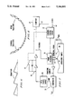
- FIG. 1 is a simplified block diagram of a scanning probe microscope incorporating the present invention.
- FIG. 2 is a simplified drawing showing a possible trajectory for the probe tip across the surface of a sample of a sample when operating according to the present invention.
- FIG. 3 is a simplified functional block diagram of of a scanning tunneling microscope incorporating the present invention.
- FIG. 4 is a simplified drawing depicting a technique employed for maximizing the speed of the scan when employing the present invention by employing adjacent scan line data to pick a minimum safe height to lift the probe during each jump.
- FIG. 5 is a simplified drawing depicting how the quasi-parabolic jump trajectory could change depending on whether the surface is falling, flat, or rising.
- FIG. 6 is a simplified drawing of a simple triangular trajectory which can be employed for the jumps if desired.
- FIG. 7 is a simplified functional block diagram of analog probe positioning apparatus for a scanning tunneling microscope incorporating the present invention.
- FIG. 8 is a simplified functional block diagram of the probe positioning apparatus of an atomic force microscope incorporating the present invention.
- FIG. 9 is a simplified functional block diagram of another embodiment of a probe positioning apparatus of an atomic force microscope according to the present invention, and which a cantilever arm is provided with a piezoelectric gauge or a strain gauge to detect the bending of the cantilever arm.
- JPM Jumping Probe Microscope
- FIG. 1 shows a block diagram of the JPM 10
- FIG. 2 shows schematically how the tip 16 of the probe 12 might move over the surface 14.
- FIG. 3 is an STM version of the JPM.
- the tunneling current between the tip 16 and surface 14 is the medium employed for detecting the surface 14 with the probe 12.
- the JPM 10 operates with the relative position of the tip 6 and sample 18 being controlled by a three-dimensional positioner 20 of a type well known in the art for such applications, with either the tip 16 or sample 18 (or both) being moved.
- a three-dimensional positioner 20 of a type well known in the art for such applications, with either the tip 16 or sample 18 (or both) being moved.
- the tip 16 is moved by the scanning control circuitry 32 in a raster scan, faster in X than in Y, to trace out frames of data, much like an image is traced out on a television screen. This horizontal motion can be continuous or in steps.
- the tip 16 is preferably controlled by the piezoelectric positioner 20 which is, in turn, controlled by a control circuit 22 which controls the motion of the tip 16 in Z, i.e. the vertical direction.
- the trajectory of the tip 16 is one which will quickly lift the tip 16 away from the surface 14 and then bring it back down as the tip 16 is moving in the X direction.
- the surface detecting electronics 24 are looking for a threshold tunneling current which indicates that the tip 16 is within about 2.0 nanometers of the surface 14. When this occurs as detected by the comparator 38, the X and Z positions of the tip 16 are recorded in the data storage memory 34 and the tip 16 is then be lifted up into another up-and-down trajectory.
- the trajectories all be a constant distance in X since the computer 26 can sort the data from memory 34 out later and interpolate to make an X-Y grid of surface 14 height; in fact, it would occur that the spacing in X between the data points is closer for a surface 14 that is rising in X than for a surface 14 falling in X if the trajectories have the same shape.
- the tunneling current may be detected again as the tip is being raised and the tip can be raised again before it is lowered. That is, the raising could occur in several steps before the tip is lowered when the tip is going up a steep feature on the surface.
- the time at which a tunneling current between the tip 16 and surface 14 occurs gives the position of the tip 16 in X.
- the position is Y is usually assumed to be constant during one scan line and can be either a continuous slow motion or incremented at the end of each scan line, as desired by the implementor.
- the increment could be a jump, or series or jumps, as is done in the X direction.
- there will be more jump data points than the number of points in the image so that each image data point can be an average or just one of the jump data points which have occurred from the last image data point.
- the positioner 20 (which as mentioned earlier is preferably a piezoelectric device), the inventors herein have found that it is best to raise the tip 16 on each jump only enough to clear the surface 14 until the next touchdown on the surface 14. Also, for reasons of speed, the tip 16 should not be moved excessively since it takes a finite time to start and stop the motion. This start and stop time increases when the motion increases.
- a typical positioner 20 might have a vertical sensitivity of 10 nanometers/volt of applied voltage and the maximum voltage available might be 300 volts.
- the jump voltage to move the tip 16 off the surface 14 would be a small fraction of this 300 volts, say only about 1 volts, which would lift the tip 16 10 nanometers off the surface 14, about five times the normal tip to surface distance for an STM.
- This height for the preferred embodiment is controlled by a digital signal processor 28 within the surface detecting electronics 24 which is, in turn, controlled by software 30 in the computer 26 that the user can manipulate to vary operation according to the circumstances in order to get optimum performance.
- the jump height can be varied to suit the surface 14 being scanned, being larger for rougher surfaces.
- the vertical resolution of the height measurement of the surface 14 is much better than the jump height since the data of the height of the surface 14 is obtained only at a particular point in the jump, say when the tip 16 comes near the surface and a tunneling current is established, i.e. only at the end of the trajectories.
- This tunneling current occurs only when the tip 16 is a few nanometers from the surface 14; so, the resolution is a few nanometers if the height of the tip 16 is recorded when a tunneling current occurs, over a wide range of currents.
- tip 16 it is not necessary that tip 16 be brought down to this particular height above the surface 14 since the height data obtained at any tunneling current can be corrected mathematically by the computer 26 to a height at some other tunneling current.
- the variation of the tunneling current with height can be measured by the JPM 10 simply by moving the tip 16 off the surface 14 in small steps and recording the current. During the jumping motion, the tip 16 can be brought down in fairly large steps, say one nanometer, in order to increase the speed. Since the tunneling current varies, substantially over this distance, the current detected, when it occurs, will not be the same for each data point.
- the height can be corrected to a fixed tunneling current by the computer 26, giving a vertical height resolution much better than one nanometer, even though the tip 16 is brought down in steps of one nanometer. Higher speeds could be obtained by having the tip 16 move down in fairly large steps, stop when a tunneling current is detected, and then using the magnitude of the tunneling current to correct the height to a fixed current to obtain a high resolution constant current topography.
- An alternate way of operating the JPM is to not synchronize the data taking with the jump trajectory, but to oversample the data so that several sampling data points per jump, or per image point, are taken.
- the actual data point which is used could then be the lowest value or most negative of these sampling data points so that the actual data is the lowest point in the trajectory of each jump.
- This method has also been implemented by the inventors using a high speed digital signal processor to take in the sampling data points and find the lowest point to use as the actual data point. This is not as satisfactory as sampling the data at the bottom of each trajectory but is simple to implement in some systems and is a major improvement over standard feedback systems.
- the above-described feedback system for the Jumping Probe Microscope 10 is quite different from that of prior art Scanning Probe Microscopes where the attempt is made to have the probe 12 scan along and follow the surface 14.
- the feedback system of the JPM in a sense, oscillates the tip 16 up and down near the surface 14 but in a very intelligent way such that the surface 14 height can be determined at the end of each oscillation so that the resolution of the device is much better than the size of the oscillations.
- the feedback system operates with a feedback gain which is low enough that the probe 12 will not oscillate in Z.
- the Jumping Probe Microscope 10 of this invention typically uses an asymmetric gain in which a high gain, or high speed motion, is used for raising the tip 16 and a low gain, or low speed motion, is used for lowering it.
- the bottom envelope of the oscillations is used as the height data for the surface 14 so that the oscillations themselves do not appear as noise in the data, as happens in normal systems. This is much different than including the oscillations in the data and then filtering to obtain a mean since in that case the lateral resolution would be decreased by the filtering, giving an image with little detail. In the JPM 10, no filtering of the data is needed and the lateral resolution is good to one jump of the probe 12.
- the inventors herein have operated the JPM 10 in the mode of a very high gain non-linear feedback system where as soon as the tunneling current exceeds a threshold, the height of the tip 16 is recorded in memory 34 and a large gain is applied to the vertical positioner 20 of the tip 16 to lift the tip 16.
- a smaller gain is applied to bring the tip 16 down to the surface 14 in a controlled (and safe to both the probe 12 and surface 14) manner. This results in the tip being jerked away from the surface quickly and then brought down at a slower rate to produce an arc-like trajectory.
- the computer 26 of the JPM 10 itself could adjust the jump height to match the sample 18, data point by data point, by using data from the present and/or previous scan line or scan frame to anticipate the topography of the surface 14.
- FIG. 4 shows how this could be done.
- the height of the surface 14 of the sample 18 being scanned as measured from the present or previous scan line or lines is stored in memory 34. Since the topography is similar from one scan line to the next, the data from the previous scan line(s) can be used to calculate the anticipated height of the next data point. This can be done simply by using the height of the corresponding data point from the previous scan line.
- This anticipated value of the height of the next point can then be used by the above-described control circuit components of the JPM 10 to choose the trajectory for the next jump so that the tip 16 will avoid the surface 14, but not excessively, on the way to the next data point. For example, if the surface 14 is sloping downward, the trajectory can be more shallow than if the surface 14 is sloping upwards, as shown in FIG. 6.
- the different trajectories that the tip 16 goes through could be looked up from a table or could be calculated from a formula (as simple as just a variable height jump which depends on previous topography). Such techniques are well known to those skilled in the art and, therefore, will not be described in any detail in the interest of simplicity and the avoidance of redundancy. Again, remembering that excessive motion is lost time, the intent is that the JPM 10 learn from previous data how to jump the tip 16 to the next data point so that excessive motion does not occur. In this manner, large rises in the surface 14 can be anticipated and the trajectory chosen to not collide the tip 16 with the surface 14, even on high speed scans.
- the trajectory can be made quite simple.
- the tip 16 can be moved up by a fixed step in Z, horizontally by a fixed step in X, and then lowered until a tunneling current is detected, the Z position recorded, and then the process started all over. These motions could overlap in time.
- the Y position can be incremented by a fixed amount, or Y can be slowly varied during each scan line. The inventors have found in their tests that it is best that the steps in X be done at a constant rate, otherwise the creep of the piezoelectric positioner 20 will affect the image.
- the trajectory could also be done using analog electronics for the vertical positioning of the tip 16 as shown in FIG. 7.
- the Z (vertical) position of the tip 16 is controlled by an integrator 36 in which a current is leaked off at a rate controlled by the user to lower the tip 16.
- the tip 16 is close enough to the surface 14 for a tunneling current to flow from the surface 14 of the sample 18 to the tip 16 and be sensed by the comparator 38, the height of the tip 16 (Z control voltage) is recorded and the tip 16 raised by a charge pulsed into the integrator 36 from source 40. The amount of this charge can be user-controlled to control the height the tip 16 is raised.
- the current leakage is stopped by opening the switch 42 so that the tip 16 remains above the surface 14.
- a clock running at some pre-established rate, is input at 44 and moves the tip 16 in the X direction and also starts lowering the tip 16 by closing the switch which leaks charge from the integrator 36, and then the foregoing series of events repeats.
- Y is incremented and the scan in X is reversed. In this way, the tip 16 is scanned in a raster fashion across the surface 14 with data giving the height of the surface 14 each time the tip 16 comes within tunneling distance of the surface 14.
- the tip 16 could be moved continuously in X with jump data points being recorded each time a tunneling current is detected and the data collection system, usually and preferably the computer 26, could make an image array out of the unequally spaced jump data points.
- the computer could record X, Y and Z to produce an image of the surface.
- An analog JPM could be operated with a nonlinear feedback system in which the gain is large whenever the tunneling current or error signal is above some threshold, and is smaller whenever the tunneling current or error signal is below some threshold.
- FIG. 8 An atomic force microscope version of the Jumping Probe Microscope 10 of this invention is shown in FIG. 8, where it is generally indicated as 10'.
- the sample 18 is scanned in X and Y and served in Z while the bending of the arm 46 which holds the tip 16 is detected by the deflection of a beam of light 48 bounced off the back of the arm 46 to detector 50.
- the output of the detector 50 (which is an analog signal reflecting the position of the beam of light 48 on the surface of the detector and, therefore, the angle of reflection of the beam of light 48 as related to the bending of the arm 46) is converted to a digital signal in the A/D converter 52.
- the digital value of the bending of the arm 46 from the A/D converter 52 is then input to computing electronics and memory substantially as described above with respect to the previous embodiment (generally indicated by box 54) which provides the necessary X, Y, and Z control signals to a piezoelectric positioner 20' used to scan the sample 18 with respect to the stationary probe 12.
- the AFM is even more sensitive to tip 16 damage than the STM. Accordingly, the jumping of the tip 16 on the surface 14 according to the techniques of the present invention will greatly help for large scans.
- the sample 18 is raised toward the tip 16 by the positioner 20' until the force of contact reaches a certain value, at which time the height of the sample 18 (vertical control signal) is recorded and the sample 18 moved away from the tip 16 and also moved in the X direction in order to repeat the sequence and obtain another data point.
- the foregoing jump scan process then continues, producing a raster scan of the surface 14 with the tip 16 touching the surface 14 at each data point where the height of the surface 14 is recorded.
- the probe when looking at samples which are loose, such as DNA on a flat surface, the probe tends to push the sample around.
- the present JPM invention will minimize this problem by "poking" at the sample instead of “brushing” it to determine the shape of the sample.
- the tip 16 does not touch the surface 14; but, it is desirable to position the tip 16 very close to the surface 14 to get good spatial resolution.
- the surface 14 is brought close to the tip 16 and the arm 46 bends down as the tip 16 is attracted to the surface 14. Then, at some predetermined bending of the arm 46, the height of the sample 18 is recorded and the sample 18 then moved away from the tip 16 and moved in X to repeat the sequence.
- Such attractive mode microscopes can, for example, use a ferromagnetic tip 16 to map out the magnetic attractions, and therefore magnetic fields, over the surface 14 of a sample 18. If the arm holding the tip were instrumented with a strain gauge or piezoelectric gauge which are schematically indicated in FIG. 9 by reference numeral designation 45, or the like, to detect the bending of the arm, then the arm could be scanned back and forth, as in the STM, over a stationary sample.
- the present invention has met its stated objectives by providing a new approach to scanning probe microscopes which provides the benefits thereof in the various approaches to such devices presently known in the art. It is also anticipated that its benefits will be equally applicable to variation in the art of scanning probe microscopes presently under development and, as yet, unavailable commercially.
Abstract
Description
Claims (19)
Priority Applications (2)
| Application Number | Priority Date | Filing Date | Title |
|---|---|---|---|
| US08/009,076 US5266801A (en) | 1989-06-05 | 1993-01-26 | Jumping probe microscope |
| US08/147,571 US5415027A (en) | 1989-06-05 | 1993-11-05 | Jumping probe microscope |
Applications Claiming Priority (2)
| Application Number | Priority Date | Filing Date | Title |
|---|---|---|---|
| US07/361,545 US5229606A (en) | 1989-06-05 | 1989-06-05 | Jumping probe microscope |
| US08/009,076 US5266801A (en) | 1989-06-05 | 1993-01-26 | Jumping probe microscope |
Related Parent Applications (1)
| Application Number | Title | Priority Date | Filing Date |
|---|---|---|---|
| US07/361,545 Continuation US5229606A (en) | 1989-06-05 | 1989-06-05 | Jumping probe microscope |
Related Child Applications (1)
| Application Number | Title | Priority Date | Filing Date |
|---|---|---|---|
| US08/147,571 Continuation US5415027A (en) | 1989-06-05 | 1993-11-05 | Jumping probe microscope |
Publications (1)
| Publication Number | Publication Date |
|---|---|
| US5266801A true US5266801A (en) | 1993-11-30 |
Family
ID=26679015
Family Applications (2)
| Application Number | Title | Priority Date | Filing Date |
|---|---|---|---|
| US08/009,076 Expired - Lifetime US5266801A (en) | 1989-06-05 | 1993-01-26 | Jumping probe microscope |
| US08/147,571 Expired - Lifetime US5415027A (en) | 1989-06-05 | 1993-11-05 | Jumping probe microscope |
Family Applications After (1)
| Application Number | Title | Priority Date | Filing Date |
|---|---|---|---|
| US08/147,571 Expired - Lifetime US5415027A (en) | 1989-06-05 | 1993-11-05 | Jumping probe microscope |
Country Status (1)
| Country | Link |
|---|---|
| US (2) | US5266801A (en) |
Cited By (99)
| Publication number | Priority date | Publication date | Assignee | Title |
|---|---|---|---|---|
| US5383354A (en) * | 1993-12-27 | 1995-01-24 | Motorola, Inc. | Process for measuring surface topography using atomic force microscopy |
| US5408094A (en) * | 1992-05-07 | 1995-04-18 | Olympus Optical Co., Ltd. | Atomic force microscope with light beam emission at predetermined angle |
| US5412980A (en) * | 1992-08-07 | 1995-05-09 | Digital Instruments, Inc. | Tapping atomic force microscope |
| US5440920A (en) * | 1994-02-03 | 1995-08-15 | Molecular Imaging Systems | Scanning force microscope with beam tracking lens |
| US5444244A (en) * | 1993-06-03 | 1995-08-22 | Park Scientific Instruments Corporation | Piezoresistive cantilever with integral tip for scanning probe microscope |
| US5450746A (en) * | 1993-10-12 | 1995-09-19 | The University Of North Carolina | Constant force stylus profiling apparatus and method |
| US5463897A (en) * | 1993-08-17 | 1995-11-07 | Digital Instruments, Inc. | Scanning stylus atomic force microscope with cantilever tracking and optical access |
| US5489339A (en) * | 1993-03-10 | 1996-02-06 | Seiko Instruments Inc. | Microelectronic processing machine |
| US5513518A (en) * | 1994-05-19 | 1996-05-07 | Molecular Imaging Corporation | Magnetic modulation of force sensor for AC detection in an atomic force microscope |
| US5515719A (en) * | 1994-05-19 | 1996-05-14 | Molecular Imaging Corporation | Controlled force microscope for operation in liquids |
| DE19502822A1 (en) * | 1995-01-30 | 1996-08-01 | Alexander Draebenstedt | Distance dependent signal extraction to regulate distance between probe point and probed surface for raster probe microscopy |
| WO1996024026A1 (en) * | 1995-01-31 | 1996-08-08 | Digital Instruments, Inc. | Tapping atomic force microscope with phase or frequency detection |
| USRE35317E (en) * | 1991-07-26 | 1996-08-27 | The Arizona Board Of Regents | Potentiostatic preparation of molecular adsorbates for scanning probe microscopy |
| US5583286A (en) * | 1994-08-24 | 1996-12-10 | Olympus Optical Co., Ltd. | Integrated sensor for scanning probe microscope |
| US5705814A (en) * | 1995-08-30 | 1998-01-06 | Digital Instruments, Inc. | Scanning probe microscope having automatic probe exchange and alignment |
| US5753814A (en) * | 1994-05-19 | 1998-05-19 | Molecular Imaging Corporation | Magnetically-oscillated probe microscope for operation in liquids |
| US5805448A (en) * | 1995-03-10 | 1998-09-08 | Molecular Imaging Corporation | Hybrid control system for scanning probe microscopes |
| US5856617A (en) * | 1997-09-02 | 1999-01-05 | International Business Machines Corporation | Atomic force microscope system with cantilever having unbiased spin valve magnetoresistive strain gauge |
| US5866805A (en) * | 1994-05-19 | 1999-02-02 | Molecular Imaging Corporation Arizona Board Of Regents | Cantilevers for a magnetically driven atomic force microscope |
| US5866807A (en) * | 1997-02-04 | 1999-02-02 | Digital Instruments | Method and apparatus for measuring mechanical properties on a small scale |
| US5866806A (en) * | 1996-10-11 | 1999-02-02 | Kla-Tencor Corporation | System for locating a feature of a surface |
| US5874734A (en) * | 1996-12-31 | 1999-02-23 | Elings; Virgil B. | Atomic force microscope for measuring properties of dielectric and insulating layers |
| US5874668A (en) * | 1995-10-24 | 1999-02-23 | Arch Development Corporation | Atomic force microscope for biological specimens |
| US5948972A (en) * | 1994-12-22 | 1999-09-07 | Kla-Tencor Corporation | Dual stage instrument for scanning a specimen |
| US6008489A (en) * | 1997-12-03 | 1999-12-28 | Digital Instruments | Method for improving the operation of oscillating mode atomic force microscopes |
| USRE36488E (en) * | 1992-08-07 | 2000-01-11 | Veeco Instruments Inc. | Tapping atomic force microscope with phase or frequency detection |
| US6038916A (en) * | 1997-07-22 | 2000-03-21 | Digital Instruments | Method and apparatus for measuring energy dissipation by a probe during operation of an atomic force microscope |
| WO2000046568A2 (en) * | 1999-02-08 | 2000-08-10 | Zakrytoe Aktsionernoe Obschestvo 'avtex Ltd' | Method of information collection and processing of sample's surface |
| EP1045253A2 (en) * | 1999-03-31 | 2000-10-18 | Agency of Industrial Science and Technology of Ministry of International Trade and Industry | Prober for electrical measurements and method of measuring electrical characteristics with said prober |
| US6148662A (en) * | 1996-06-17 | 2000-11-21 | Industrial Technology Research Institute | High-sensitivity strain probe |
| US6172506B1 (en) | 1997-07-15 | 2001-01-09 | Veeco Instruments Inc. | Capacitance atomic force microscopes and methods of operating such microscopes |
| US6185992B1 (en) | 1999-07-15 | 2001-02-13 | Veeco Instruments Inc. | Method and system for increasing the accuracy of a probe-based instrument measuring a heated sample |
| US6280939B1 (en) | 1998-09-01 | 2001-08-28 | Veeco Instruments, Inc. | Method and apparatus for DNA sequencing using a local sensitive force detector |
| US6357285B1 (en) | 1998-11-09 | 2002-03-19 | Veeco Instruments Inc. | Method and apparatus for the quantitative and objective correlation of data from a local sensitive force detector |
| US6365895B1 (en) * | 1998-01-22 | 2002-04-02 | Matsushita Electric Industrial Co., Ltd. | Apparatus for measuring a micro surface configuration and a method for manufacturing a probe incorporated in this measuring apparatus |
| US6427345B1 (en) | 1998-11-10 | 2002-08-06 | Veeco Instruments, Inc. | Method and apparatus for a line based, two-dimensional characterization of a three-dimensional surface |
| US6441371B1 (en) | 2000-04-03 | 2002-08-27 | Korea Institute Of Science And Technology | Scanning probe microscope |
| US20030028345A1 (en) * | 1999-12-20 | 2003-02-06 | Watkins Arthur D. | Device for self-verifying temperature measurement and control |
| US6520005B2 (en) | 1994-12-22 | 2003-02-18 | Kla-Tencor Corporation | System for sensing a sample |
| US20030041657A1 (en) * | 2001-08-21 | 2003-03-06 | Degertekin F. Levent | Method and apparatus for the ultrasonic actuation of the cantilever of a probe-based instrument |
| US6590208B2 (en) | 2001-01-19 | 2003-07-08 | Veeco Instruments Inc. | Balanced momentum probe holder |
| US20030222635A1 (en) * | 1991-01-28 | 2003-12-04 | Jacobsen Stephen C. | Movement actuator/sensor systems |
| US6667467B2 (en) * | 2000-03-13 | 2003-12-23 | Seiko Instruments Inc. | Microprobe and scanning probe apparatus having microprobe |
| US6694817B2 (en) | 2001-08-21 | 2004-02-24 | Georgia Tech Research Corporation | Method and apparatus for the ultrasonic actuation of the cantilever of a probe-based instrument |
| US20050009197A1 (en) * | 2003-02-11 | 2005-01-13 | Adams Jesse D. | Chemical sensor with oscillating cantilevered probe and mechanical stop |
| WO2005003821A2 (en) | 2003-06-03 | 2005-01-13 | Bay Materials Llc | Phase change sensor |
| US20050006986A1 (en) * | 2001-12-07 | 2005-01-13 | Pasi Kallio | Micromanupulator including piezoelectric benders |
| US20050028583A1 (en) * | 2002-07-02 | 2005-02-10 | Chanmin Su | Method and apparatus of driving torsional resonance mode of a probe-based instrument |
| US20050034529A1 (en) * | 2003-05-07 | 2005-02-17 | Hongxing Tang | Strain sensors based on nanowire piezoresistor wires and arrays |
| US6873163B2 (en) | 2001-01-18 | 2005-03-29 | The Trustees Of The University Of Pennsylvania | Spatially resolved electromagnetic property measurement |
| US20050194534A1 (en) * | 2004-01-14 | 2005-09-08 | Eric Kneedler | Method of operating a probe microscope |
| US20050199047A1 (en) * | 2003-03-11 | 2005-09-15 | Adams Jesse D. | Liquid cell and passivated probe for atomic force microscopy and chemical sensing |
| US20050212529A1 (en) * | 2002-07-02 | 2005-09-29 | Lin Huang | Method and apparatus for measuring electrical properties in torsional resonance mode |
| US20060000263A1 (en) * | 2004-04-14 | 2006-01-05 | Veeco Instruments Inc. | Method and apparatus for obtaining quantitative measurements using a probe based instrument |
| WO2006005619A1 (en) | 2004-07-14 | 2006-01-19 | Universität Kassel | A method of aligning a first article relative to a second article and an apparatus for aligning a first article relative to a second article |
| US20060011830A1 (en) * | 2002-08-30 | 2006-01-19 | Yoshiharu Shirakawabe | Method of manufacturing the multi-tip probe, a multi-tip probe, and surface characteristic analysis apparatus |
| US20060191329A1 (en) * | 1999-03-29 | 2006-08-31 | Adderton Dennis M | Dynamic activation for an atomic force microscope and method of use thereof |
| US20060230474A1 (en) * | 2005-04-12 | 2006-10-12 | Mininni Paul I | Method and apparatus for rapid automatic engagement of a prove |
| US20070023649A1 (en) * | 2005-07-29 | 2007-02-01 | West Paul E | Scanning probe microscope control system |
| US20070075243A1 (en) * | 2005-09-30 | 2007-04-05 | Kneeburg David A | Scanning probe microscopy method and apparatus utilizing sample pitch |
| US20070208533A1 (en) * | 2002-05-06 | 2007-09-06 | Dahlen Gregory A | Image reconstruction method |
| US20070220958A1 (en) * | 2006-03-21 | 2007-09-27 | Veeco Instruments Inc. | Optical detection alignment/tracking method and apparatus |
| US20070251305A1 (en) * | 2006-04-26 | 2007-11-01 | Veeco Instruments Lnc. | Method and Apparatus for Reducing Lateral Interactive Forces During Operation of a Probe-Based Instrument |
| US20080011065A1 (en) * | 2006-07-12 | 2008-01-17 | Chanmin Su | Thermal mechanical drive actuator, thermal probe and method of thermally driving a probe |
| US20080087077A1 (en) * | 2006-10-17 | 2008-04-17 | Mininni Paul L | Method and apparatus of scanning a sample using a scanning probe microscope |
| US20080121813A1 (en) * | 2006-11-03 | 2008-05-29 | Young James M | Method and apparatus of compensating for position shift |
| US20080127722A1 (en) * | 2006-11-30 | 2008-06-05 | Chanmin Su | Method and apparatus for obtaining material property information of a heterogeneous sample using harmonic resonance imaging |
| US20080154521A1 (en) * | 2006-12-22 | 2008-06-26 | Tianming Bao | Systems and methods for utilizing scanning probe shape characterization |
| US20080179206A1 (en) * | 2006-06-26 | 2008-07-31 | Veeco Instruments Inc. | Apparatus and method of transporting and loading probe devices of a metrology instrument |
| US20080216583A1 (en) * | 2003-05-07 | 2008-09-11 | California Institute Of Technology | Detection of Resonator Motion Using Piezoresistive Signal Downmixing |
| US20080223119A1 (en) * | 2007-03-16 | 2008-09-18 | Veeco Instruments Inc. | Fast-Scanning SPM Scanner and Method of Operating Same |
| US7434476B2 (en) * | 2003-05-07 | 2008-10-14 | Califronia Institute Of Technology | Metallic thin film piezoresistive transduction in micromechanical and nanomechanical devices and its application in self-sensing SPM probes |
| US20090031792A1 (en) * | 2007-08-02 | 2009-02-05 | Wenjun Fan | Probe Device for a Metrology Instrument and Method of Fabricating the Same |
| US20090205092A1 (en) * | 2007-12-28 | 2009-08-13 | Veeco Instruments Inc. | Method of fabricating a probe device for a metrology instrument and a probe device produced thereby |
| EP2101181A1 (en) | 2008-03-12 | 2009-09-16 | Capres A/S | Device including a contact detector |
| US20090324450A1 (en) * | 1995-07-24 | 2009-12-31 | General Nanotechnology, L.L.C. | Nanometer Scale Instrument for Biochemically, Chemically, or Catalytically Interacting with a Sample Material |
| US20100071098A1 (en) * | 2008-05-13 | 2010-03-18 | Northwestern University | Scanning probe epitaxy |
| US7694346B2 (en) | 2004-10-01 | 2010-04-06 | Board Of Regents Of The Nevada System Of Higher Education On Behalf Of The University Of Nevada | Cantilevered probe detector with piezoelectric element |
| US20100122385A1 (en) * | 2008-11-13 | 2010-05-13 | Veeco Instruments Inc. | Method and apparatus of operating a scanning probe microscope |
| US20100141291A1 (en) * | 2007-03-12 | 2010-06-10 | Petersen Dirch H | Device including a contact detector |
| US7770231B2 (en) | 2007-08-02 | 2010-08-03 | Veeco Instruments, Inc. | Fast-scanning SPM and method of operating same |
| US20110167524A1 (en) * | 2008-11-13 | 2011-07-07 | Bruker Nano, Inc. | Method and apparatus of operating a scanning probe microscope |
| US20120242189A1 (en) * | 2011-03-24 | 2012-09-27 | Nanoworld Ag | Micro-mechanical component with cantilever integrated electrical functional element |
| US8524501B2 (en) | 2003-10-17 | 2013-09-03 | Board Of Regents Of The Nevada System Of Higher Education | Self-sensing array of microcantilevers for chemical detection |
| US8650660B2 (en) | 2008-11-13 | 2014-02-11 | Bruker Nano, Inc. | Method and apparatus of using peak force tapping mode to measure physical properties of a sample |
| US8782811B2 (en) | 2011-04-29 | 2014-07-15 | Bruker Nano, Inc. | Cleaning station for atomic force microscope |
| WO2014144496A1 (en) | 2013-03-15 | 2014-09-18 | Bruker Nano, Inc. | Chemical nano-identification of a sample using normalized near-field spectroscopy |
| US8904560B2 (en) | 2007-05-07 | 2014-12-02 | Bruker Nano, Inc. | Closed loop controller and method for fast scanning probe microscopy |
| US8955161B2 (en) | 2008-11-13 | 2015-02-10 | Bruker Nano, Inc. | Peakforce photothermal-based detection of IR nanoabsorption |
| US9052336B2 (en) | 2013-03-08 | 2015-06-09 | Bruker Nano, Inc. | Method and apparatus of physical property measurement using a probe-based nano-localized light source |
| US9097737B2 (en) | 2013-11-25 | 2015-08-04 | Oxford Instruments Asylum Research, Inc. | Modular atomic force microscope with environmental controls |
| US9274139B2 (en) | 2008-11-13 | 2016-03-01 | Bruker Nano, Inc. | Method and apparatus of operating a scanning probe microscope |
| US9291639B2 (en) | 2013-03-15 | 2016-03-22 | Bruker Nano, Inc. | Dual-probe scanning probe microscope |
| US9739799B2 (en) | 2014-02-28 | 2017-08-22 | Bruker Nano, Inc. | Method and apparatus to compensate for deflection artifacts in an atomic force microscope |
| EP3293527A2 (en) | 2012-06-22 | 2018-03-14 | Bruker Nano, Inc. | Method and apparatus of electrical property measurement using an afm operating in peak force tapping mode |
| WO2019191037A1 (en) | 2018-03-26 | 2019-10-03 | Bruker Nano, Inc. | Large radius probe |
| WO2020227222A1 (en) | 2019-05-03 | 2020-11-12 | Bruker Nano, Inc. | Torsion wing probe assembly |
| US10845382B2 (en) | 2016-08-22 | 2020-11-24 | Bruker Nano, Inc. | Infrared characterization of a sample using oscillating mode |
| WO2022258084A1 (en) | 2021-07-13 | 2022-12-15 | Ceske Vysoke Uceni Technicke V Praze | A method of examining a sample in an atomic force microscope |
Families Citing this family (16)
| Publication number | Priority date | Publication date | Assignee | Title |
|---|---|---|---|---|
| JPH0642953A (en) * | 1992-07-24 | 1994-02-18 | Matsushita Electric Ind Co Ltd | Interatomic force microscope |
| US5400647A (en) * | 1992-11-12 | 1995-03-28 | Digital Instruments, Inc. | Methods of operating atomic force microscopes to measure friction |
| US5681987A (en) * | 1993-04-28 | 1997-10-28 | Topometrix Corporation | Resonance contact scanning force microscope |
| US5481908A (en) * | 1993-04-28 | 1996-01-09 | Topometrix Corporation | Resonance contact scanning force microscope |
| US6266581B1 (en) * | 1996-05-10 | 2001-07-24 | The United States Of America As Represented By The Secretary Of Commerce | Spatial RAM for high precision data acquisition systems |
| US5773824A (en) * | 1997-04-23 | 1998-06-30 | International Business Machines Corporation | Method for improving measurement accuracy using active lateral scanning control of a probe |
| US5801381A (en) * | 1997-05-21 | 1998-09-01 | International Business Machines Corporation | Method for protecting a probe tip using active lateral scanning control |
| US5902928A (en) * | 1997-06-02 | 1999-05-11 | International Business Machines Corporation | Controlling engagement of a scanning microscope probe with a segmented piezoelectric actuator |
| US5918274A (en) * | 1997-06-02 | 1999-06-29 | International Business Machines Corporation | Detecting fields with a single-pass, dual-amplitude-mode scanning force microscope |
| JP3406236B2 (en) * | 1998-02-19 | 2003-05-12 | セイコーインスツルメンツ株式会社 | Scanning probe microscope measuring method and apparatus |
| WO2008042009A1 (en) * | 2006-03-13 | 2008-04-10 | Asylum Research Corporation | Nanoindenter |
| US7406860B2 (en) | 2006-04-28 | 2008-08-05 | Seagate Technology Llc | Atomic force microscopy scanning and image processing |
| GB0801900D0 (en) | 2008-02-01 | 2008-03-12 | Imp Innovations Ltd | Scanning probe microscopy |
| US8525112B2 (en) * | 2010-08-10 | 2013-09-03 | Seagate Technology Llc | Variable pixel density imaging |
| US9586817B2 (en) | 2011-07-28 | 2017-03-07 | Seagate Technology Llc | Semi-auto scanning probe microscopy scanning |
| US20130081159A1 (en) * | 2011-07-29 | 2013-03-28 | Seagate Technology Llc | Advanced atomic force microscopy scanning for obtaining a true shape |
Citations (23)
| Publication number | Priority date | Publication date | Assignee | Title |
|---|---|---|---|---|
| US2405133A (en) * | 1942-10-07 | 1946-08-06 | Brush Dev Co | Method and means for measuring surface roughness |
| US2460726A (en) * | 1943-01-11 | 1949-02-01 | Brush Dev Co | Surface roughness measuring device |
| US3049002A (en) * | 1959-02-24 | 1962-08-14 | Hediger Hermann | Device for measuring the roughness of surfaces |
| US3378648A (en) * | 1964-12-31 | 1968-04-16 | Gen Electric | Doped piezoresistive phonograph pickup |
| US4106333A (en) * | 1975-08-12 | 1978-08-15 | Ernst Salje | Method of and apparatus for examining the roughness of surfaces |
| US4359892A (en) * | 1979-12-15 | 1982-11-23 | U.S. Philips Corporation | Arrangement for measuring surface profiles |
| US4618767A (en) * | 1985-03-22 | 1986-10-21 | International Business Machines Corporation | Low-energy scanning transmission electron microscope |
| US4665313A (en) * | 1985-06-28 | 1987-05-12 | International Business Machines Corporation | Apparatus and method for displaying hole-electron pair distributions induced by electron bombardment |
| US4724318A (en) * | 1985-11-26 | 1988-02-09 | International Business Machines Corporation | Atomic force microscope and method for imaging surfaces with atomic resolution |
| US4814622A (en) * | 1987-11-06 | 1989-03-21 | Bell Communications Research, Inc. | High speed scanning tunneling microscope |
| US4823004A (en) * | 1987-11-24 | 1989-04-18 | California Institute Of Technology | Tunnel and field effect carrier ballistics |
| US4848141A (en) * | 1988-04-06 | 1989-07-18 | Oliver Warren C | Method for continuous determination of the elastic stiffness of contact between two bodies |
| US4861990A (en) * | 1988-02-09 | 1989-08-29 | California Institute Of Technology | Tunneling susceptometry |
| SU1504485A1 (en) * | 1988-01-25 | 1989-08-30 | Пермский политехнический институт | Roughness sensor |
| US4902892A (en) * | 1987-10-15 | 1990-02-20 | Agency Of Industrial Science And Technology, Kosaka Laboratory Ltd. | Method of measurement by scanning tunneling microscope |
| US4912822A (en) * | 1988-01-27 | 1990-04-03 | Stanford University | Method of making an integrated scanning tunneling microscope |
| US4939363A (en) * | 1988-06-23 | 1990-07-03 | Director General Of Agency Of Industrial Science And Technology | Scanning tunneling microscope |
| US4985627A (en) * | 1988-08-18 | 1991-01-15 | International Business Machines Corporation | Spin-polarized scanning tunneling microscope |
| US5015850A (en) * | 1989-06-20 | 1991-05-14 | The Board Of Trustees Of The Leland Stanford Junior University | Microfabricated microscope assembly |
| US5092163A (en) * | 1990-06-27 | 1992-03-03 | Young Russell D | Precision small scale force sensor |
| US5162653A (en) * | 1988-06-02 | 1992-11-10 | Hitachi, Ltd. | Scanning tunneling microscope and surface topographic observation method |
| US5168159A (en) * | 1990-11-19 | 1992-12-01 | Olympus Optical Co., Ltd. | Barrier height measuring apparatus including a conductive cantilever functioning as a tunnelling probe |
| US5171992A (en) * | 1990-10-31 | 1992-12-15 | International Business Machines Corporation | Nanometer scale probe for an atomic force microscope, and method for making same |
Family Cites Families (3)
| Publication number | Priority date | Publication date | Assignee | Title |
|---|---|---|---|---|
| DE3675158D1 (en) * | 1985-11-26 | 1990-11-29 | Ibm | METHOD AND MICROSCOPE FOR GENERATING TOPOGRAPHIC IMAGES USING ATOMIC INTERACTIONS WITH SUB-RESOLUTION. |
| US4868396A (en) * | 1987-10-13 | 1989-09-19 | Arizona Board Of Regents, Arizona State University | Cell and substrate for electrochemical STM studies |
| JPH05196458A (en) * | 1991-01-04 | 1993-08-06 | Univ Leland Stanford Jr | Piezoresistance cantilever structure for atomic power microscope |
-
1993
- 1993-01-26 US US08/009,076 patent/US5266801A/en not_active Expired - Lifetime
- 1993-11-05 US US08/147,571 patent/US5415027A/en not_active Expired - Lifetime
Patent Citations (23)
| Publication number | Priority date | Publication date | Assignee | Title |
|---|---|---|---|---|
| US2405133A (en) * | 1942-10-07 | 1946-08-06 | Brush Dev Co | Method and means for measuring surface roughness |
| US2460726A (en) * | 1943-01-11 | 1949-02-01 | Brush Dev Co | Surface roughness measuring device |
| US3049002A (en) * | 1959-02-24 | 1962-08-14 | Hediger Hermann | Device for measuring the roughness of surfaces |
| US3378648A (en) * | 1964-12-31 | 1968-04-16 | Gen Electric | Doped piezoresistive phonograph pickup |
| US4106333A (en) * | 1975-08-12 | 1978-08-15 | Ernst Salje | Method of and apparatus for examining the roughness of surfaces |
| US4359892A (en) * | 1979-12-15 | 1982-11-23 | U.S. Philips Corporation | Arrangement for measuring surface profiles |
| US4618767A (en) * | 1985-03-22 | 1986-10-21 | International Business Machines Corporation | Low-energy scanning transmission electron microscope |
| US4665313A (en) * | 1985-06-28 | 1987-05-12 | International Business Machines Corporation | Apparatus and method for displaying hole-electron pair distributions induced by electron bombardment |
| US4724318A (en) * | 1985-11-26 | 1988-02-09 | International Business Machines Corporation | Atomic force microscope and method for imaging surfaces with atomic resolution |
| US4902892A (en) * | 1987-10-15 | 1990-02-20 | Agency Of Industrial Science And Technology, Kosaka Laboratory Ltd. | Method of measurement by scanning tunneling microscope |
| US4814622A (en) * | 1987-11-06 | 1989-03-21 | Bell Communications Research, Inc. | High speed scanning tunneling microscope |
| US4823004A (en) * | 1987-11-24 | 1989-04-18 | California Institute Of Technology | Tunnel and field effect carrier ballistics |
| SU1504485A1 (en) * | 1988-01-25 | 1989-08-30 | Пермский политехнический институт | Roughness sensor |
| US4912822A (en) * | 1988-01-27 | 1990-04-03 | Stanford University | Method of making an integrated scanning tunneling microscope |
| US4861990A (en) * | 1988-02-09 | 1989-08-29 | California Institute Of Technology | Tunneling susceptometry |
| US4848141A (en) * | 1988-04-06 | 1989-07-18 | Oliver Warren C | Method for continuous determination of the elastic stiffness of contact between two bodies |
| US5162653A (en) * | 1988-06-02 | 1992-11-10 | Hitachi, Ltd. | Scanning tunneling microscope and surface topographic observation method |
| US4939363A (en) * | 1988-06-23 | 1990-07-03 | Director General Of Agency Of Industrial Science And Technology | Scanning tunneling microscope |
| US4985627A (en) * | 1988-08-18 | 1991-01-15 | International Business Machines Corporation | Spin-polarized scanning tunneling microscope |
| US5015850A (en) * | 1989-06-20 | 1991-05-14 | The Board Of Trustees Of The Leland Stanford Junior University | Microfabricated microscope assembly |
| US5092163A (en) * | 1990-06-27 | 1992-03-03 | Young Russell D | Precision small scale force sensor |
| US5171992A (en) * | 1990-10-31 | 1992-12-15 | International Business Machines Corporation | Nanometer scale probe for an atomic force microscope, and method for making same |
| US5168159A (en) * | 1990-11-19 | 1992-12-01 | Olympus Optical Co., Ltd. | Barrier height measuring apparatus including a conductive cantilever functioning as a tunnelling probe |
Non-Patent Citations (12)
| Title |
|---|
| "A Batch-Fabricated Silicon Accelerometer", Lynn Michelle Roylance, IEEE Transactions on Electron Devices, vol. ED-26, No. 12, Dec. 1979. |
| "Atomic Force Microscope-Force Mapping and Profiling on a sub 100-A Scale", Y. Martin et al, IBM, T. J. Research Center Yorktown Hghts, N.Y., pp. 4723-4729. |
| "Force Measurement Using An AC Atomic Force Microscope", William A. Ducker, et al., J. Appl. Phys. 67 (9), May 1, 1990, New York. |
| "Investigation of Bloch Wall Fine Structures by Magnetic Force Microscopy", T. Goddenhenrich et al, Journal of Microscopy, vol. 152, Pt. 2, Nov. 1988, pp. 527-536. |
| "Potentiometry for Thin-Film Structures Using Atomic Force Microscopy," J. Vac. Sci. Technol. A, vol. 8, No. 1, Jan./Feb. 1990; pp. 394-399 Anders et al. |
| "Pressure Sensors Selection Guide PC Board Mountable", ICSENSORS, Milpitas, Calif., TO-8 Series. |
| A Batch Fabricated Silicon Accelerometer , Lynn Michelle Roylance, IEEE Transactions on Electron Devices, vol. ED 26, No. 12, Dec. 1979. * |
| Atomic Force Microscope Force Mapping and Profiling on a sub 100 A Scale , Y. Martin et al, IBM, T. J. Research Center Yorktown Hghts, N.Y., pp. 4723 4729. * |
| Force Measurement Using An AC Atomic Force Microscope , William A. Ducker, et al., J. Appl. Phys. 67 (9), May 1, 1990, New York. * |
| Investigation of Bloch Wall Fine Structures by Magnetic Force Microscopy , T. Goddenhenrich et al, Journal of Microscopy, vol. 152, Pt. 2, Nov. 1988, pp. 527 536. * |
| Potentiometry for Thin Film Structures Using Atomic Force Microscopy, J. Vac. Sci. Technol. A, vol. 8, No. 1, Jan./Feb. 1990; pp. 394 399 Anders et al. * |
| Pressure Sensors Selection Guide PC Board Mountable , ICSENSORS, Milpitas, Calif., TO 8 Series. * |
Cited By (185)
| Publication number | Priority date | Publication date | Assignee | Title |
|---|---|---|---|---|
| US6933715B2 (en) | 1991-01-28 | 2005-08-23 | Sarcos Lc | Sensor system for sensing movement |
| US20040221658A1 (en) * | 1991-01-28 | 2004-11-11 | Jacobsen Stephen C. | Movement actuator/sensor systems |
| US20030222635A1 (en) * | 1991-01-28 | 2003-12-04 | Jacobsen Stephen C. | Movement actuator/sensor systems |
| US6992474B2 (en) | 1991-01-28 | 2006-01-31 | Sarcos Lc | Movement actuator/sensor systems |
| USRE35317E (en) * | 1991-07-26 | 1996-08-27 | The Arizona Board Of Regents | Potentiostatic preparation of molecular adsorbates for scanning probe microscopy |
| US5408094A (en) * | 1992-05-07 | 1995-04-18 | Olympus Optical Co., Ltd. | Atomic force microscope with light beam emission at predetermined angle |
| US5412980A (en) * | 1992-08-07 | 1995-05-09 | Digital Instruments, Inc. | Tapping atomic force microscope |
| USRE36488E (en) * | 1992-08-07 | 2000-01-11 | Veeco Instruments Inc. | Tapping atomic force microscope with phase or frequency detection |
| US5489339A (en) * | 1993-03-10 | 1996-02-06 | Seiko Instruments Inc. | Microelectronic processing machine |
| US5444244A (en) * | 1993-06-03 | 1995-08-22 | Park Scientific Instruments Corporation | Piezoresistive cantilever with integral tip for scanning probe microscope |
| US5463897A (en) * | 1993-08-17 | 1995-11-07 | Digital Instruments, Inc. | Scanning stylus atomic force microscope with cantilever tracking and optical access |
| US5450746A (en) * | 1993-10-12 | 1995-09-19 | The University Of North Carolina | Constant force stylus profiling apparatus and method |
| US5383354A (en) * | 1993-12-27 | 1995-01-24 | Motorola, Inc. | Process for measuring surface topography using atomic force microscopy |
| US5440920A (en) * | 1994-02-03 | 1995-08-15 | Molecular Imaging Systems | Scanning force microscope with beam tracking lens |
| US5587523A (en) * | 1994-02-03 | 1996-12-24 | Molecular Imaging Corporation | Atomic force microscope employing beam tracking |
| US5763767A (en) * | 1994-02-03 | 1998-06-09 | Molecular Imaging Corp. | Atomic force microscope employing beam-tracking |
| US6134955A (en) * | 1994-05-19 | 2000-10-24 | Molecular Imaging Corporation | Magnetic modulation of force sensor for AC detection in an atomic force microscope |
| US5753814A (en) * | 1994-05-19 | 1998-05-19 | Molecular Imaging Corporation | Magnetically-oscillated probe microscope for operation in liquids |
| US5612491A (en) * | 1994-05-19 | 1997-03-18 | Molecular Imaging Corporation | Formation of a magnetic film on an atomic force microscope cantilever |
| US5515719A (en) * | 1994-05-19 | 1996-05-14 | Molecular Imaging Corporation | Controlled force microscope for operation in liquids |
| US5866805A (en) * | 1994-05-19 | 1999-02-02 | Molecular Imaging Corporation Arizona Board Of Regents | Cantilevers for a magnetically driven atomic force microscope |
| US5513518A (en) * | 1994-05-19 | 1996-05-07 | Molecular Imaging Corporation | Magnetic modulation of force sensor for AC detection in an atomic force microscope |
| US5583286A (en) * | 1994-08-24 | 1996-12-10 | Olympus Optical Co., Ltd. | Integrated sensor for scanning probe microscope |
| US7100430B2 (en) | 1994-12-22 | 2006-09-05 | Kla-Tencor Corporation | Dual stage instrument for scanning a specimen |
| US7278301B2 (en) | 1994-12-22 | 2007-10-09 | Kla-Tencor Corporation | System for sensing a sample |
| US20050005688A1 (en) * | 1994-12-22 | 2005-01-13 | Amin Samsavar | Dual stage instrument for scanning a specimen |
| US5948972A (en) * | 1994-12-22 | 1999-09-07 | Kla-Tencor Corporation | Dual stage instrument for scanning a specimen |
| US6931917B2 (en) | 1994-12-22 | 2005-08-23 | Kla-Tencor Corporation | System for sensing a sample |
| US6267005B1 (en) | 1994-12-22 | 2001-07-31 | Kla-Tencor Corporation | Dual stage instrument for scanning a specimen |
| US20040118193A1 (en) * | 1994-12-22 | 2004-06-24 | Mcwaid Thomas | System for sensing a sample |
| US6520005B2 (en) | 1994-12-22 | 2003-02-18 | Kla-Tencor Corporation | System for sensing a sample |
| DE19502822A1 (en) * | 1995-01-30 | 1996-08-01 | Alexander Draebenstedt | Distance dependent signal extraction to regulate distance between probe point and probed surface for raster probe microscopy |
| WO1996024026A1 (en) * | 1995-01-31 | 1996-08-08 | Digital Instruments, Inc. | Tapping atomic force microscope with phase or frequency detection |
| US5805448A (en) * | 1995-03-10 | 1998-09-08 | Molecular Imaging Corporation | Hybrid control system for scanning probe microscopes |
| US8046843B2 (en) * | 1995-07-24 | 2011-10-25 | General Nanotechnology Llc | Nanometer scale instrument for biochemically, chemically, or catalytically interacting with a sample material |
| US20090324450A1 (en) * | 1995-07-24 | 2009-12-31 | General Nanotechnology, L.L.C. | Nanometer Scale Instrument for Biochemically, Chemically, or Catalytically Interacting with a Sample Material |
| US5705814A (en) * | 1995-08-30 | 1998-01-06 | Digital Instruments, Inc. | Scanning probe microscope having automatic probe exchange and alignment |
| US5874668A (en) * | 1995-10-24 | 1999-02-23 | Arch Development Corporation | Atomic force microscope for biological specimens |
| US6148662A (en) * | 1996-06-17 | 2000-11-21 | Industrial Technology Research Institute | High-sensitivity strain probe |
| US5866806A (en) * | 1996-10-11 | 1999-02-02 | Kla-Tencor Corporation | System for locating a feature of a surface |
| US5874734A (en) * | 1996-12-31 | 1999-02-23 | Elings; Virgil B. | Atomic force microscope for measuring properties of dielectric and insulating layers |
| US5866807A (en) * | 1997-02-04 | 1999-02-02 | Digital Instruments | Method and apparatus for measuring mechanical properties on a small scale |
| US6172506B1 (en) | 1997-07-15 | 2001-01-09 | Veeco Instruments Inc. | Capacitance atomic force microscopes and methods of operating such microscopes |
| US6038916A (en) * | 1997-07-22 | 2000-03-21 | Digital Instruments | Method and apparatus for measuring energy dissipation by a probe during operation of an atomic force microscope |
| US5856617A (en) * | 1997-09-02 | 1999-01-05 | International Business Machines Corporation | Atomic force microscope system with cantilever having unbiased spin valve magnetoresistive strain gauge |
| US6008489A (en) * | 1997-12-03 | 1999-12-28 | Digital Instruments | Method for improving the operation of oscillating mode atomic force microscopes |
| US6365895B1 (en) * | 1998-01-22 | 2002-04-02 | Matsushita Electric Industrial Co., Ltd. | Apparatus for measuring a micro surface configuration and a method for manufacturing a probe incorporated in this measuring apparatus |
| US6621080B2 (en) | 1998-01-22 | 2003-09-16 | Matsushita Electric Industrial Co., Ltd. | Apparatus for measuring a micro surface configuration and a method for manufacturing a probe incorporated in this measuring apparatus |
| US6280939B1 (en) | 1998-09-01 | 2001-08-28 | Veeco Instruments, Inc. | Method and apparatus for DNA sequencing using a local sensitive force detector |
| US6357285B1 (en) | 1998-11-09 | 2002-03-19 | Veeco Instruments Inc. | Method and apparatus for the quantitative and objective correlation of data from a local sensitive force detector |
| US6427345B1 (en) | 1998-11-10 | 2002-08-06 | Veeco Instruments, Inc. | Method and apparatus for a line based, two-dimensional characterization of a three-dimensional surface |
| US6776030B1 (en) * | 1999-02-08 | 2004-08-17 | Zakrytoye aktsionernoye obschestvo “Autex Ltd” | Method of information collection and processing of sample's surface |
| WO2000046568A3 (en) * | 1999-02-08 | 2000-12-21 | Alexei Petrovich Kirpichnikov | Method of information collection and processing of sample's surface |
| WO2000046568A2 (en) * | 1999-02-08 | 2000-08-10 | Zakrytoe Aktsionernoe Obschestvo 'avtex Ltd' | Method of information collection and processing of sample's surface |
| US20060191329A1 (en) * | 1999-03-29 | 2006-08-31 | Adderton Dennis M | Dynamic activation for an atomic force microscope and method of use thereof |
| US7204131B2 (en) | 1999-03-29 | 2007-04-17 | Veeco Instruments Inc. | Dynamic activation for an atomic force microscope and method of use thereof |
| EP1045253A2 (en) * | 1999-03-31 | 2000-10-18 | Agency of Industrial Science and Technology of Ministry of International Trade and Industry | Prober for electrical measurements and method of measuring electrical characteristics with said prober |
| EP1045253A3 (en) * | 1999-03-31 | 2003-12-17 | National Institute of Advanced Industrial Science and Technology, Independent Administrative Institution | Prober for electrical measurements and method of measuring electrical characteristics with said prober |
| US6185992B1 (en) | 1999-07-15 | 2001-02-13 | Veeco Instruments Inc. | Method and system for increasing the accuracy of a probe-based instrument measuring a heated sample |
| US6389886B2 (en) | 1999-07-15 | 2002-05-21 | Veeco Instruments Inc. | Method and system for increasing the accuracy of a probe-based instrument measuring a heated sample |
| US20030028345A1 (en) * | 1999-12-20 | 2003-02-06 | Watkins Arthur D. | Device for self-verifying temperature measurement and control |
| US6667467B2 (en) * | 2000-03-13 | 2003-12-23 | Seiko Instruments Inc. | Microprobe and scanning probe apparatus having microprobe |
| US6441371B1 (en) | 2000-04-03 | 2002-08-27 | Korea Institute Of Science And Technology | Scanning probe microscope |
| US7078896B2 (en) | 2001-01-18 | 2006-07-18 | The Trustees Of The University Of Pennsylvania | Spatially resolved electromagnetic property measurement |
| US6873163B2 (en) | 2001-01-18 | 2005-03-29 | The Trustees Of The University Of Pennsylvania | Spatially resolved electromagnetic property measurement |
| US20050174130A1 (en) * | 2001-01-18 | 2005-08-11 | Trustees Of The University Of Pennsylvania | Spatially resolved electromagnetic property measurement |
| US6861649B2 (en) | 2001-01-19 | 2005-03-01 | Veeco Instruments, Inc. | Balanced momentum probe holder |
| US7219538B2 (en) | 2001-01-19 | 2007-05-22 | Veeco Instruments, Inc. | Balanced momentum probe holder |
| US20040069944A1 (en) * | 2001-01-19 | 2004-04-15 | Veeco Instruments, Inc. | Balanced momentum probe holder |
| US6590208B2 (en) | 2001-01-19 | 2003-07-08 | Veeco Instruments Inc. | Balanced momentum probe holder |
| US20060043286A1 (en) * | 2001-01-19 | 2006-03-02 | Veeco Instruments, Inc. | Balanced momentum probe holder |
| US6779387B2 (en) | 2001-08-21 | 2004-08-24 | Georgia Tech Research Corporation | Method and apparatus for the ultrasonic actuation of the cantilever of a probe-based instrument |
| US20030041657A1 (en) * | 2001-08-21 | 2003-03-06 | Degertekin F. Levent | Method and apparatus for the ultrasonic actuation of the cantilever of a probe-based instrument |
| US6694817B2 (en) | 2001-08-21 | 2004-02-24 | Georgia Tech Research Corporation | Method and apparatus for the ultrasonic actuation of the cantilever of a probe-based instrument |
| US7141914B2 (en) * | 2001-12-07 | 2006-11-28 | Chip-Man Technologies Oy | Micromanipulator including piezoelectric benders |
| US20050006986A1 (en) * | 2001-12-07 | 2005-01-13 | Pasi Kallio | Micromanupulator including piezoelectric benders |
| US20070208533A1 (en) * | 2002-05-06 | 2007-09-06 | Dahlen Gregory A | Image reconstruction method |
| US7684956B2 (en) | 2002-05-06 | 2010-03-23 | Veeco Instruments, Inc. | Image reconstruction method |
| US20070119241A1 (en) * | 2002-07-02 | 2007-05-31 | Chanmin Su | Method and apparatus of driving torsional resonance mode of a probe-based instrument |
| US7757544B2 (en) | 2002-07-02 | 2010-07-20 | Veeco Instruments Inc. | Method and apparatus for measuring electrical properties in torsional resonance mode |
| US20050212529A1 (en) * | 2002-07-02 | 2005-09-29 | Lin Huang | Method and apparatus for measuring electrical properties in torsional resonance mode |
| US7574903B2 (en) | 2002-07-02 | 2009-08-18 | Veeco Instruments Inc. | Method and apparatus of driving torsional resonance mode of a probe-based instrument |
| US7155964B2 (en) | 2002-07-02 | 2007-01-02 | Veeco Instruments Inc. | Method and apparatus for measuring electrical properties in torsional resonance mode |
| US7168301B2 (en) | 2002-07-02 | 2007-01-30 | Veeco Instruments Inc. | Method and apparatus of driving torsional resonance mode of a probe-based instrument |
| US20050028583A1 (en) * | 2002-07-02 | 2005-02-10 | Chanmin Su | Method and apparatus of driving torsional resonance mode of a probe-based instrument |
| US7337656B2 (en) * | 2002-08-30 | 2008-03-04 | Sii Nanotechnology Inc. | Surface characteristic analysis apparatus |
| US20060011830A1 (en) * | 2002-08-30 | 2006-01-19 | Yoshiharu Shirakawabe | Method of manufacturing the multi-tip probe, a multi-tip probe, and surface characteristic analysis apparatus |
| US20050009197A1 (en) * | 2003-02-11 | 2005-01-13 | Adams Jesse D. | Chemical sensor with oscillating cantilevered probe and mechanical stop |
| US7521257B2 (en) | 2003-02-11 | 2009-04-21 | The Board Of Regents Of The Nevada System Of Higher Education On Behalf Of The University Of Nevada, Reno | Chemical sensor with oscillating cantilevered probe and mechanical stop |
| US7260980B2 (en) | 2003-03-11 | 2007-08-28 | Adams Jesse D | Liquid cell and passivated probe for atomic force microscopy and chemical sensing |
| US10156585B2 (en) | 2003-03-11 | 2018-12-18 | Board Of Regents Of The Nevada System Of Higher Education, On Behalf Of The University Of Nevada, Reno | Cantilevered probes having piezoelectric layer, treated section, and resistive heater, and method of use for chemical detection |
| US8136385B2 (en) | 2003-03-11 | 2012-03-20 | Board of Regents of the Nevada System of Higher Education, on Behalf of the University of the University of Nevada, Reno | Cantilevered probes having piezoelectric layer, treated section, and resistive heater, and method of use for chemical detection |
| US20050199047A1 (en) * | 2003-03-11 | 2005-09-15 | Adams Jesse D. | Liquid cell and passivated probe for atomic force microscopy and chemical sensing |
| US20080216583A1 (en) * | 2003-05-07 | 2008-09-11 | California Institute Of Technology | Detection of Resonator Motion Using Piezoresistive Signal Downmixing |
| US7434476B2 (en) * | 2003-05-07 | 2008-10-14 | Califronia Institute Of Technology | Metallic thin film piezoresistive transduction in micromechanical and nanomechanical devices and its application in self-sensing SPM probes |
| US7302856B2 (en) | 2003-05-07 | 2007-12-04 | California Institute Of Technology | Strain sensors based on nanowire piezoresistor wires and arrays |
| US7617736B2 (en) | 2003-05-07 | 2009-11-17 | California Institute Of Technology | Metallic thin film piezoresistive transduction in micromechanical and nanomechanical devices and its application in self-sensing SPM probes |
| US20090038404A1 (en) * | 2003-05-07 | 2009-02-12 | California Institute Of Technology | Metallic thin film piezoresistive transduction in micromechanical and nanomechanical devices and its application in self-sensing spm probes |
| US20050034529A1 (en) * | 2003-05-07 | 2005-02-17 | Hongxing Tang | Strain sensors based on nanowire piezoresistor wires and arrays |
| US7552645B2 (en) | 2003-05-07 | 2009-06-30 | California Institute Of Technology | Detection of resonator motion using piezoresistive signal downmixing |
| US20070249059A1 (en) * | 2003-06-03 | 2007-10-25 | Stewart Ray F | Phase change sensor |
| US7794657B2 (en) | 2003-06-03 | 2010-09-14 | Cantimer, Inc. | Phase change sensor |
| WO2005003821A2 (en) | 2003-06-03 | 2005-01-13 | Bay Materials Llc | Phase change sensor |
| US20050164299A1 (en) * | 2003-06-03 | 2005-07-28 | Bay Materials Llc | Phase change sensor |
| US8524501B2 (en) | 2003-10-17 | 2013-09-03 | Board Of Regents Of The Nevada System Of Higher Education | Self-sensing array of microcantilevers for chemical detection |
| US20050194534A1 (en) * | 2004-01-14 | 2005-09-08 | Eric Kneedler | Method of operating a probe microscope |
| US7596990B2 (en) | 2004-04-14 | 2009-10-06 | Veeco Instruments, Inc. | Method and apparatus for obtaining quantitative measurements using a probe based instrument |
| US20060000263A1 (en) * | 2004-04-14 | 2006-01-05 | Veeco Instruments Inc. | Method and apparatus for obtaining quantitative measurements using a probe based instrument |
| US20110219635A1 (en) * | 2004-07-14 | 2011-09-15 | Universitat Kassel | Method of aligning a first article relative to a second article and an apparatus for aligning a first article relative to a second article |
| WO2006005619A1 (en) | 2004-07-14 | 2006-01-19 | Universität Kassel | A method of aligning a first article relative to a second article and an apparatus for aligning a first article relative to a second article |
| US20070248892A1 (en) * | 2004-07-14 | 2007-10-25 | Ivo Rangelow | A method of aligning a first article relative to a second article and an apparatus for aligning a first article relative to a second article |
| US7946029B2 (en) | 2004-07-14 | 2011-05-24 | Universitat Kassel | Apparatus for aligning a first article relative to a second article |
| US10025207B2 (en) * | 2004-07-14 | 2018-07-17 | Universität Kassel | Method of aligning a first article relative to a second article |
| US10473636B2 (en) | 2004-10-01 | 2019-11-12 | Board Of Regents Of The Nevada System Of Higher Education, On Behalf Of The University Of Nevada | Cantilevered probe detector with piezoelectric element |
| US8434161B1 (en) | 2004-10-01 | 2013-04-30 | Board Of Regents Of The Nevada System Of Higher Education, On Behalf Of The University Of Nevada | Cantilevered probe detector with piezoelectric element |
| US8434160B1 (en) | 2004-10-01 | 2013-04-30 | Board Of Regents Of The Nevada System Of Higher Education, On Behalf Of The University Of Nevada | Cantilevered probe detector with piezoelectric element |
| US7694346B2 (en) | 2004-10-01 | 2010-04-06 | Board Of Regents Of The Nevada System Of Higher Education On Behalf Of The University Of Nevada | Cantilevered probe detector with piezoelectric element |
| US8713711B2 (en) | 2004-10-01 | 2014-04-29 | Board Of Regents Of The Nevada System Of Higher Education, On Behalf Of The University Of Nevada | Cantilevered probe detector with piezoelectric element |
| US20060230474A1 (en) * | 2005-04-12 | 2006-10-12 | Mininni Paul I | Method and apparatus for rapid automatic engagement of a prove |
| US7665349B2 (en) | 2005-04-12 | 2010-02-23 | Veeco Instruments Inc. | Method and apparatus for rapid automatic engagement of a probe |
| US20070023649A1 (en) * | 2005-07-29 | 2007-02-01 | West Paul E | Scanning probe microscope control system |
| US7435955B2 (en) * | 2005-07-29 | 2008-10-14 | West Paul E | Scanning probe microscope control system |
| US7429732B2 (en) * | 2005-09-30 | 2008-09-30 | Veeco Instruments Inc. | Scanning probe microscopy method and apparatus utilizing sample pitch |
| US20070075243A1 (en) * | 2005-09-30 | 2007-04-05 | Kneeburg David A | Scanning probe microscopy method and apparatus utilizing sample pitch |
| US7478552B2 (en) | 2006-03-21 | 2009-01-20 | Veeco Instruments Inc. | Optical detection alignment/tracking method and apparatus |
| US20070220958A1 (en) * | 2006-03-21 | 2007-09-27 | Veeco Instruments Inc. | Optical detection alignment/tracking method and apparatus |
| US7607342B2 (en) | 2006-04-26 | 2009-10-27 | Vecco Instruments, Inc. | Method and apparatus for reducing lateral interactive forces during operation of a probe-based instrument |
| US20070251305A1 (en) * | 2006-04-26 | 2007-11-01 | Veeco Instruments Lnc. | Method and Apparatus for Reducing Lateral Interactive Forces During Operation of a Probe-Based Instrument |
| US7908909B2 (en) | 2006-06-26 | 2011-03-22 | Bruker Nano, Inc. | Apparatus and method of transporting and loading probe devices of a metrology instrument |
| US20080179206A1 (en) * | 2006-06-26 | 2008-07-31 | Veeco Instruments Inc. | Apparatus and method of transporting and loading probe devices of a metrology instrument |
| US7748260B2 (en) | 2006-07-12 | 2010-07-06 | Veeco Instruments Inc. | Thermal mechanical drive actuator, thermal probe and method of thermally driving a probe |
| US20080011065A1 (en) * | 2006-07-12 | 2008-01-17 | Chanmin Su | Thermal mechanical drive actuator, thermal probe and method of thermally driving a probe |
| US7770439B2 (en) | 2006-10-17 | 2010-08-10 | Veeco Instruments Inc. | Method and apparatus of scanning a sample using a scanning probe microscope |
| US20080087077A1 (en) * | 2006-10-17 | 2008-04-17 | Mininni Paul L | Method and apparatus of scanning a sample using a scanning probe microscope |
| US8050802B2 (en) | 2006-11-03 | 2011-11-01 | Bruker Nano, Inc. | Method and apparatus of compensating for position shift |
| US20080121813A1 (en) * | 2006-11-03 | 2008-05-29 | Young James M | Method and apparatus of compensating for position shift |
| US20080127722A1 (en) * | 2006-11-30 | 2008-06-05 | Chanmin Su | Method and apparatus for obtaining material property information of a heterogeneous sample using harmonic resonance imaging |
| US7617719B2 (en) | 2006-11-30 | 2009-11-17 | The Dow Chemical Company | Method and apparatus for obtaining material property information of a heterogeneous sample using harmonic resonance imaging |
| US20080154521A1 (en) * | 2006-12-22 | 2008-06-26 | Tianming Bao | Systems and methods for utilizing scanning probe shape characterization |
| US7578176B2 (en) | 2006-12-22 | 2009-08-25 | Veeco Metrology, Inc. | Systems and methods for utilizing scanning probe shape characterization |
| US8058886B2 (en) | 2007-03-12 | 2011-11-15 | Capres A/S | Device including a contact detector |
| US20100141291A1 (en) * | 2007-03-12 | 2010-06-10 | Petersen Dirch H | Device including a contact detector |
| US20080223119A1 (en) * | 2007-03-16 | 2008-09-18 | Veeco Instruments Inc. | Fast-Scanning SPM Scanner and Method of Operating Same |
| US8166567B2 (en) | 2007-03-16 | 2012-04-24 | Bruker Nano, Inc. | Fast-scanning SPM scanner and method of operating same |
| US8443459B2 (en) | 2007-03-16 | 2013-05-14 | Bruker Nano, Inc. | Fast-scanning SPM scanner and method of operating same |
| US9244096B2 (en) | 2007-05-07 | 2016-01-26 | Bruke Nano, Inc. | Closed loop controller and method for fast scanning probe microscopy |
| US8904560B2 (en) | 2007-05-07 | 2014-12-02 | Bruker Nano, Inc. | Closed loop controller and method for fast scanning probe microscopy |
| US7823216B2 (en) * | 2007-08-02 | 2010-10-26 | Veeco Instruments Inc. | Probe device for a metrology instrument and method of fabricating the same |
| US7770231B2 (en) | 2007-08-02 | 2010-08-03 | Veeco Instruments, Inc. | Fast-scanning SPM and method of operating same |
| US20090031792A1 (en) * | 2007-08-02 | 2009-02-05 | Wenjun Fan | Probe Device for a Metrology Instrument and Method of Fabricating the Same |
| US20090205092A1 (en) * | 2007-12-28 | 2009-08-13 | Veeco Instruments Inc. | Method of fabricating a probe device for a metrology instrument and a probe device produced thereby |
| US8595860B2 (en) | 2007-12-28 | 2013-11-26 | Bruker Nano, Inc. | Method of fabricating a probe device for a metrology instrument and a probe device produced thereby |
| EP2101181A1 (en) | 2008-03-12 | 2009-09-16 | Capres A/S | Device including a contact detector |
| US20100071098A1 (en) * | 2008-05-13 | 2010-03-18 | Northwestern University | Scanning probe epitaxy |
| US8650660B2 (en) | 2008-11-13 | 2014-02-11 | Bruker Nano, Inc. | Method and apparatus of using peak force tapping mode to measure physical properties of a sample |
| US20100122385A1 (en) * | 2008-11-13 | 2010-05-13 | Veeco Instruments Inc. | Method and apparatus of operating a scanning probe microscope |
| US8739309B2 (en) | 2008-11-13 | 2014-05-27 | Bruker Nano, Inc. | Method and apparatus of operating a scanning probe microscope |
| US8646109B2 (en) | 2008-11-13 | 2014-02-04 | Bruker Nano, Inc. | Method and apparatus of operating a scanning probe microscope |
| US9322842B2 (en) | 2008-11-13 | 2016-04-26 | Bruker Nano, Inc. | Method and apparatus of operating a scanning probe microscope |
| US8955161B2 (en) | 2008-11-13 | 2015-02-10 | Bruker Nano, Inc. | Peakforce photothermal-based detection of IR nanoabsorption |
| US9995765B2 (en) | 2008-11-13 | 2018-06-12 | Bruker Nano, Inc. | Method and apparatus of using peak force tapping mode to measure physical properties of a sample |
| US9810713B2 (en) | 2008-11-13 | 2017-11-07 | Bruker Nano, Inc. | Method and apparatus of operating a scanning probe microscope |
| US9207167B2 (en) | 2008-11-13 | 2015-12-08 | Bruker Nano, Inc. | Peak force photothermal-based detection of IR nanoabsorption |
| US9213047B2 (en) | 2008-11-13 | 2015-12-15 | Bruker Nano, Inc. | Method and apparatus of electrical property measurement using an AFM operating in peak force tapping mode |
| US20110167524A1 (en) * | 2008-11-13 | 2011-07-07 | Bruker Nano, Inc. | Method and apparatus of operating a scanning probe microscope |
| US9274139B2 (en) | 2008-11-13 | 2016-03-01 | Bruker Nano, Inc. | Method and apparatus of operating a scanning probe microscope |
| US9291640B2 (en) | 2008-11-13 | 2016-03-22 | Bruker Nano, Inc. | Method and apparatus of using peak force tapping mode to measure physical properties of a sample |
| US8810110B2 (en) * | 2011-03-24 | 2014-08-19 | Nanoworld Ag | Micro-mechanical component with cantilever integrated electrical functional element |
| US20120242189A1 (en) * | 2011-03-24 | 2012-09-27 | Nanoworld Ag | Micro-mechanical component with cantilever integrated electrical functional element |
| US8782811B2 (en) | 2011-04-29 | 2014-07-15 | Bruker Nano, Inc. | Cleaning station for atomic force microscope |
| EP3293527A2 (en) | 2012-06-22 | 2018-03-14 | Bruker Nano, Inc. | Method and apparatus of electrical property measurement using an afm operating in peak force tapping mode |
| US9052336B2 (en) | 2013-03-08 | 2015-06-09 | Bruker Nano, Inc. | Method and apparatus of physical property measurement using a probe-based nano-localized light source |
| EP3467518A1 (en) | 2013-03-15 | 2019-04-10 | Bruker Nano, Inc. | Chemical nano-identification of a sample using normalized near-field spectroscopy |
| WO2014144496A1 (en) | 2013-03-15 | 2014-09-18 | Bruker Nano, Inc. | Chemical nano-identification of a sample using normalized near-field spectroscopy |
| US9291639B2 (en) | 2013-03-15 | 2016-03-22 | Bruker Nano, Inc. | Dual-probe scanning probe microscope |
| EP4345463A2 (en) | 2013-03-15 | 2024-04-03 | Bruker Nano, Inc. | Chemical nano-identification of a sample using normalized near-field spectroscopy |
| US9097737B2 (en) | 2013-11-25 | 2015-08-04 | Oxford Instruments Asylum Research, Inc. | Modular atomic force microscope with environmental controls |
| US10416190B2 (en) | 2013-11-25 | 2019-09-17 | Oxford Instruments Asylum Research Inc | Modular atomic force microscope with environmental controls |
| US9581616B2 (en) | 2013-11-25 | 2017-02-28 | Oxford Instruments Asylum Research, Inc | Modular atomic force microscope with environmental controls |
| US9739799B2 (en) | 2014-02-28 | 2017-08-22 | Bruker Nano, Inc. | Method and apparatus to compensate for deflection artifacts in an atomic force microscope |
| US10845382B2 (en) | 2016-08-22 | 2020-11-24 | Bruker Nano, Inc. | Infrared characterization of a sample using oscillating mode |
| WO2019191037A1 (en) | 2018-03-26 | 2019-10-03 | Bruker Nano, Inc. | Large radius probe |
| WO2020227222A1 (en) | 2019-05-03 | 2020-11-12 | Bruker Nano, Inc. | Torsion wing probe assembly |
| JP2022530987A (en) * | 2019-05-03 | 2022-07-05 | ブルカー ナノ インコーポレイテッド | Torsion wing probe assembly |
| WO2022258084A1 (en) | 2021-07-13 | 2022-12-15 | Ceske Vysoke Uceni Technicke V Praze | A method of examining a sample in an atomic force microscope |
Also Published As
| Publication number | Publication date |
|---|---|
| US5415027A (en) | 1995-05-16 |
Similar Documents
| Publication | Publication Date | Title |
|---|---|---|
| US5266801A (en) | Jumping probe microscope | |
| US5229606A (en) | Jumping probe microscope | |
| US5412980A (en) | Tapping atomic force microscope | |
| US5418363A (en) | Scanning probe microscope using stored data for vertical probe positioning | |
| EP0839312B1 (en) | Tapping atomic force microscope with phase or frequency detection | |
| USRE36488E (en) | Tapping atomic force microscope with phase or frequency detection | |
| US5329808A (en) | Atomic force microscope | |
| US7278301B2 (en) | System for sensing a sample | |
| KR100961571B1 (en) | Scanning probe microscope | |
| Sulchek et al. | Characterization and optimization of scan speed for tapping-mode atomic force microscopy | |
| KR101324598B1 (en) | Method and apparatus of scanning a sample using a scanning probe microscope | |
| US4954704A (en) | Method to increase the speed of a scanning probe microscope | |
| US5237859A (en) | Atomic force microscope | |
| US6518570B1 (en) | Sensing mode atomic force microscope | |
| US4987303A (en) | Micro-displacement detector device, piezo-actuator provided with the micro-displacement detector device and scanning probe microscope provided with the piezo-actuator | |
| JPH10332715A (en) | Field detection by single path double amplitude mode scanning force microscope | |
| JP3515364B2 (en) | Apparatus, method and recording medium for examining topographical characteristics of sample surface | |
| JPH09281118A (en) | Scanning type probe microscope |
Legal Events
| Date | Code | Title | Description |
|---|---|---|---|
| STCF | Information on status: patent grant |
Free format text: PATENTED CASE |
|
| CC | Certificate of correction | ||
| FEPP | Fee payment procedure |
Free format text: PAYOR NUMBER ASSIGNED (ORIGINAL EVENT CODE: ASPN); ENTITY STATUS OF PATENT OWNER: LARGE ENTITY |
|
| FPAY | Fee payment |
Year of fee payment: 4 |
|
| FEPP | Fee payment procedure |
Free format text: PAYOR NUMBER ASSIGNED (ORIGINAL EVENT CODE: ASPN); ENTITY STATUS OF PATENT OWNER: LARGE ENTITY |
|
| FEPP | Fee payment procedure |
Free format text: PAYER NUMBER DE-ASSIGNED (ORIGINAL EVENT CODE: RMPN); ENTITY STATUS OF PATENT OWNER: LARGE ENTITY Free format text: PAT HLDR NO LONGER CLAIMS SMALL ENT STAT AS SMALL BUSINESS (ORIGINAL EVENT CODE: LSM2); ENTITY STATUS OF PATENT OWNER: LARGE ENTITY |
|
| REFU | Refund |
Free format text: REFUND - PAYMENT OF MAINTENANCE FEE, 8TH YR, SMALL ENTITY (ORIGINAL EVENT CODE: R284); ENTITY STATUS OF PATENT OWNER: LARGE ENTITY |
|
| FPAY | Fee payment |
Year of fee payment: 8 |
|
| AS | Assignment |
Owner name: VEECO INSTRUMENTS INC., NEW YORK Free format text: MERGER;ASSIGNOR:DIGITAL INSTRUMENTS, INC.;REEL/FRAME:014059/0376 Effective date: 19980529 |
|
| FPAY | Fee payment |
Year of fee payment: 12 |
|
| AS | Assignment |
Owner name: VEECO METROLOGY INC., CALIFORNIA Free format text: ASSIGNMENT OF ASSIGNORS INTEREST;ASSIGNOR:VEECO INSTRUMENTS INC.;REEL/FRAME:025051/0290 Effective date: 20100928 |
|
| AS | Assignment |
Owner name: BRUKER NANO, INC., CALIFORNIA Free format text: CHANGE OF NAME;ASSIGNOR:VEECO METROLOGY INC.;REEL/FRAME:027111/0461 Effective date: 20101007 |