US5266842A - Charge pump circuit for a substrate voltage generator - Google Patents
Charge pump circuit for a substrate voltage generator Download PDFInfo
- Publication number
- US5266842A US5266842A US07/924,747 US92474792A US5266842A US 5266842 A US5266842 A US 5266842A US 92474792 A US92474792 A US 92474792A US 5266842 A US5266842 A US 5266842A
- Authority
- US
- United States
- Prior art keywords
- electrode
- pumping capacitor
- pumping
- transistor
- capacitor
- Prior art date
- Legal status (The legal status is an assumption and is not a legal conclusion. Google has not performed a legal analysis and makes no representation as to the accuracy of the status listed.)
- Expired - Lifetime
Links
- 239000000758 substrate Substances 0.000 title claims abstract description 80
- 238000005086 pumping Methods 0.000 claims abstract description 155
- 239000003990 capacitor Substances 0.000 claims abstract description 143
- 239000004065 semiconductor Substances 0.000 claims abstract description 7
- 230000010355 oscillation Effects 0.000 claims description 2
- 230000007704 transition Effects 0.000 claims 5
- 229910044991 metal oxide Inorganic materials 0.000 claims 2
- 150000004706 metal oxides Chemical class 0.000 claims 2
- 238000000034 method Methods 0.000 claims 2
- 102100040844 Dual specificity protein kinase CLK2 Human genes 0.000 description 14
- 101000749291 Homo sapiens Dual specificity protein kinase CLK2 Proteins 0.000 description 14
- 108091006146 Channels Proteins 0.000 description 12
- 102100040862 Dual specificity protein kinase CLK1 Human genes 0.000 description 10
- 101000749294 Homo sapiens Dual specificity protein kinase CLK1 Proteins 0.000 description 10
- 238000010586 diagram Methods 0.000 description 2
- 230000003071 parasitic effect Effects 0.000 description 2
- 102000004129 N-Type Calcium Channels Human genes 0.000 description 1
- 108090000699 N-Type Calcium Channels Proteins 0.000 description 1
- 230000000694 effects Effects 0.000 description 1
Images

Classifications
-
- G—PHYSICS
- G11—INFORMATION STORAGE
- G11C—STATIC STORES
- G11C11/00—Digital stores characterised by the use of particular electric or magnetic storage elements; Storage elements therefor
- G11C11/21—Digital stores characterised by the use of particular electric or magnetic storage elements; Storage elements therefor using electric elements
- G11C11/34—Digital stores characterised by the use of particular electric or magnetic storage elements; Storage elements therefor using electric elements using semiconductor devices
- G11C11/40—Digital stores characterised by the use of particular electric or magnetic storage elements; Storage elements therefor using electric elements using semiconductor devices using transistors
- G11C11/401—Digital stores characterised by the use of particular electric or magnetic storage elements; Storage elements therefor using electric elements using semiconductor devices using transistors forming cells needing refreshing or charge regeneration, i.e. dynamic cells
- G11C11/4063—Auxiliary circuits, e.g. for addressing, decoding, driving, writing, sensing or timing
- G11C11/407—Auxiliary circuits, e.g. for addressing, decoding, driving, writing, sensing or timing for memory cells of the field-effect type
-
- H—ELECTRICITY
- H02—GENERATION; CONVERSION OR DISTRIBUTION OF ELECTRIC POWER
- H02M—APPARATUS FOR CONVERSION BETWEEN AC AND AC, BETWEEN AC AND DC, OR BETWEEN DC AND DC, AND FOR USE WITH MAINS OR SIMILAR POWER SUPPLY SYSTEMS; CONVERSION OF DC OR AC INPUT POWER INTO SURGE OUTPUT POWER; CONTROL OR REGULATION THEREOF
- H02M3/00—Conversion of dc power input into dc power output
- H02M3/02—Conversion of dc power input into dc power output without intermediate conversion into ac
- H02M3/04—Conversion of dc power input into dc power output without intermediate conversion into ac by static converters
- H02M3/06—Conversion of dc power input into dc power output without intermediate conversion into ac by static converters using resistors or capacitors, e.g. potential divider
- H02M3/07—Conversion of dc power input into dc power output without intermediate conversion into ac by static converters using resistors or capacitors, e.g. potential divider using capacitors charged and discharged alternately by semiconductor devices with control electrode, e.g. charge pumps
- H02M3/073—Charge pumps of the Schenkel-type
-
- G—PHYSICS
- G05—CONTROLLING; REGULATING
- G05F—SYSTEMS FOR REGULATING ELECTRIC OR MAGNETIC VARIABLES
- G05F3/00—Non-retroactive systems for regulating electric variables by using an uncontrolled element, or an uncontrolled combination of elements, such element or such combination having self-regulating properties
- G05F3/02—Regulating voltage or current
- G05F3/08—Regulating voltage or current wherein the variable is dc
- G05F3/10—Regulating voltage or current wherein the variable is dc using uncontrolled devices with non-linear characteristics
- G05F3/16—Regulating voltage or current wherein the variable is dc using uncontrolled devices with non-linear characteristics being semiconductor devices
- G05F3/20—Regulating voltage or current wherein the variable is dc using uncontrolled devices with non-linear characteristics being semiconductor devices using diode- transistor combinations
- G05F3/205—Substrate bias-voltage generators
Definitions
- the present invention relates to a substrate voltage generator used in a semiconductor memory device, and more particularly to a charge pump circuit for providing the substrate with a negative voltage.
- the substrate voltage generator is used in a semiconductor memory device, to stabilize the threshold voltages of MOS transistors and to prevent the occurrence of parasitic transistors as well as malfunctioning due to the undershoot of source signals.
- MOS transistors MOS transistors
- parasitic transistors parasitic transistors
- the detector 10 detects the level to regulate the oscillator 20. Then signals generated by the oscillator drive a drive circuit 30 of the charge pump circuit 40 to convert the V BB of a substrate rode 50 to a desired level.
- the present invention is directed to the charge pump circuit 40.
- the charge pump circuit is driven by the signals CLKI to CLK4 so as to discharge current from the substrate ground, thus dropping the substrate voltage.
- the voltage of n22 (n25) is dropped to the minimum -V cc (V cc being the source voltage) by means of M22 (M25) driven by the CLK2 (CLK3)
- the voltage of n21 (n26) is also dropped to only -V cc by means of M21 (M26) driven by the CLK1 (CLK4), and therefore the V BB may not be dropped below the minimum -V cc -V TP (Here, V TP is the threshold voltage of M27, usually about 1.0V).
- this conventional circuit has a low pumping capability with a low V CC so as not to provide a stabilized substrate voltage.
- a substrate voltage generator which comprises an oscillation circuit for producing square waves of a given frequency, drive circuit for receiving the square waves to produce clock signals CLKI to CLK4 of square waves and substrate node V BB for transferring a given substrate voltage, is provided with a charge pump circuit comprising:
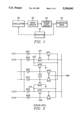
- FIG. 1 is a block diagram for illustrating the system of a substrate voltage generator
- FIG. 2 schematically shows a conventional charge pump circuit
- FIG. 3 schematically shows a charge pump circuit according to the present invention
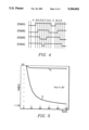
- FIG. 4 is a timing diagram for illustrating the input clock pulses in the inventive circuit.
- one electrode of a first pumping capacitor M1 is connected to the CLKI signal, that of a second pumping capacitor M2 to the CLK2 signal, that of a third pumping capacitor M3 to the CLK3 signal, that of a fourth pumping capacitor M4 to the CLK2 signal, that of a fifth pumping capacitor M5 to the CLK3 signal, and that of a sixth pumping capacitor M6 to the CLK4 signal.
- a first transistor M11 has a gate connected to the other electrode of the fifth pumping capacitor M5 and a channel formed between the other electrode of the first pumping capacitor M1 and the substrate node (V BB )
- a second transistor M14 has a gate connected to the other electrode of the second pumping capacitor M2 and a channel formed between the other electrode of the sixth pumping capacitor M6 and the substrate node V BB . Also provided is a circuit connected between the other electrodes of the pumping capacitors and the substrate node V BB for making the voltage of the substrate node V BB have a negative value.
- the circuit for making the voltage of the substrate node V BB have a negative value comprises third to tenth transistors M7, M8, M9, M10, M12, M13, M15, and M16.
- the third transistor M7 has a gate connected to the other electrode of the first pumping capacitor M1 and a channel formed between the other electrode of the second pumping capacitor M2 and the substrate node V BB .
- the fourth transistor M8 has a gate connected to the other electrode of the third pumping capacitor M3 and a channel formed between the other electrode of the second pumping capacitor M2 and ground.
- the fifth transistor M9 has a gate connected to the other electrode of the fourth pumping capacitor M4 and a channel formed between the other electrode of the fifth pumping capacitor M5 and ground.
- the sixth transistor M10 has a gate connected to the other electrode of the sixth pumping capacitor M6 and a channel formed between the other electrode of the fifth pumping capacitor M5 and the substrate node V BB .
- a seventh transistor M12 has a gate connected to the substrate node V BB and a channel formed between the other electrodes of the third and fifth pumping capacitors M3 and M5.
- An eighth transistor M13 has a gate connected to the substrate node V BB and a channel formed between the other electrodes of the second and fourth pumping capacitors M2 and M4.
- the ninth transistor M15 has a gate connected to the other electrode of the first pumping capacitor Ml and a channel formed between the other electrodes of the first and second pumping capacitors Ml and M2.
- the tenth transistor M16 has a gate connected to the other electrode of the sixth pumping capacitor M6 and a channel formed between the other electrodes of the fifth and sixth pumping capacitors M5 and M6.
- the essential point of the present invention consists in the circuit connection of the terminals of the transistors M11 and M14.
- FIG. 3 The circuit of FIG. 3 is driven by the clock signals CLKI to CLK4 as shown in FIG. 3.
- node n1 In the timing interval A, the voltage of node n1 is -V CC +V TP , so that the third transistor M7 is turned on. Hence, a current flows from the substrate node V BB to make node n2 have a voltage of the substrate node V BB . Meanwhile, node n6 is pre-charged with voltage V TP via the second transistor M14 and node n5 is discharged via the fifth transistor M9 to have the ground voltage.
- the first clock CLK1 is changed from 0V to V CC , so that the voltage of node n1 is changed to V TP to turn off the third transistor M7.
- the second clock CLK2 is changed from 0V to V CC in the timing interval C, thus making the voltage of the node n2 have V BB +V CC .
- the third CLK3 is changed from V CC to 0V in the timing interval D, the voltage of the node n2 is discharged via the fourth transistor M8 to ground voltage, and the voltage of the node n5 is changed to -V CC .
- the fourth clock CLK4 is changed from V CC to 0V to make the voltage of the node n6 have -V CC +V TP , thus completely turning on the sixth transistor M10 so as to change the voltage of the node n5 to V BB .
- the fourth clock CLK4 is changed from 0V to V CC so as to change the voltage of the node n6 to V TP , thus turning off the sixth transistor M10, in the timing interval F.
- the third clock CLK3 is changed from 0V to V CC so as to change the voltage of the node n5 from V BB to V BB +V CC .
- timing interval H the second clock CLK2 is changed from V CC to 0V so as to change the voltages of the nodes n2 and n4 to V CC , thus turning on the fifth transistor M9.
- the voltage of the node n5 is discharged to ground voltage, so that the charge pump circuit performs the charge pumping twice during a period.
- the inventive circuit works quickly to make the V BB have a desired negative voltage as contrasted with a conventional circuit, (a).
- the source voltage V CC is 1.5V and the input clock period is 0.5 ⁇ s.
- the present invention enhances the charge pumping capability, so that the substrate voltage is stabilized even in a lower level of the source voltage at which the semiconductor devices work as well as reducing the power consumption in stand-by.
Abstract
Description
Claims (18)
Applications Claiming Priority (2)
| Application Number | Priority Date | Filing Date | Title |
|---|---|---|---|
| KR91-18834 | 1991-10-25 | ||
| KR1019910018834A KR940005691B1 (en) | 1991-10-25 | 1991-10-25 | Charge pumping circuit of the substrate-voltage generating device |
Publications (1)
| Publication Number | Publication Date |
|---|---|
| US5266842A true US5266842A (en) | 1993-11-30 |
Family
ID=19321777
Family Applications (1)
| Application Number | Title | Priority Date | Filing Date |
|---|---|---|---|
| US07/924,747 Expired - Lifetime US5266842A (en) | 1991-10-25 | 1992-08-04 | Charge pump circuit for a substrate voltage generator |
Country Status (3)
| Country | Link |
|---|---|
| US (1) | US5266842A (en) |
| JP (1) | JPH0777076B2 (en) |
| KR (1) | KR940005691B1 (en) |
Cited By (27)
| Publication number | Priority date | Publication date | Assignee | Title |
|---|---|---|---|---|
| US5343088A (en) * | 1992-03-30 | 1994-08-30 | Samsung Electronics Co. Ltd. | Charge pump circuit for a substrate voltage generator of a semiconductor memory device |
| US5381051A (en) * | 1993-03-08 | 1995-01-10 | Motorola Inc. | High voltage charge pump |
| US5412257A (en) * | 1992-10-20 | 1995-05-02 | United Memories, Inc. | High efficiency N-channel charge pump having a primary pump and a non-cascaded secondary pump |
| US5493249A (en) * | 1993-12-06 | 1996-02-20 | Micron Technology, Inc. | System powered with inter-coupled charge pumps |
| US5502415A (en) * | 1992-11-18 | 1996-03-26 | Oki Electric Industry Co., Ltd. | Booster power generating circuit |
| US5583384A (en) * | 1995-06-07 | 1996-12-10 | National Semiconductor Corporation | Method and apparatus for connecting and disconnecting a power field effect transistor |
| US5642073A (en) * | 1993-12-06 | 1997-06-24 | Micron Technology, Inc. | System powered with inter-coupled charge pumps |
| US5701096A (en) * | 1994-12-09 | 1997-12-23 | Fujitsu Limited | Charge-pump type booster circuit |
| US5767736A (en) * | 1995-11-27 | 1998-06-16 | Lucent Technologies Inc. | Charge pump having high switching speed and low switching noise |
| US5838190A (en) * | 1995-10-14 | 1998-11-17 | Hyundai Electronics Industries, Co., Ltd. | Negative voltage drive circuit |
| US5838189A (en) * | 1994-12-21 | 1998-11-17 | Samsung Electronics Co., Ltd. | Substrate voltage generating circuit of semiconductor memory device |
| US5874850A (en) * | 1994-08-12 | 1999-02-23 | Stmicroelectronics S.R.L. | Mos voltage elevator of the charge pump type |
| US5939935A (en) * | 1996-08-08 | 1999-08-17 | Micron Technology, Inc | Charge pump |
| US6002355A (en) * | 1997-06-26 | 1999-12-14 | Cirrus Logic, Inc. | Synchronously pumped substrate analog-to-digital converter (ADC) system and methods |
| US6016073A (en) * | 1996-11-14 | 2000-01-18 | Sgs-Thomson Microelectronics S.R.L. | BiCMOS negative charge pump |
| US6052022A (en) * | 1997-04-30 | 2000-04-18 | Samsung Electronics Co., Ltd. | Voltage boosting circuits having over-voltage protection circuits therein |
| US6064250A (en) * | 1996-07-29 | 2000-05-16 | Townsend And Townsend And Crew Llp | Various embodiments for a low power adaptive charge pump circuit |
| US6072358A (en) * | 1998-01-16 | 2000-06-06 | Altera Corporation | High voltage pump circuit with reduced oxide stress |
| US6107863A (en) * | 1997-02-03 | 2000-08-22 | Matsushita Electric Industrial Co., Ltd. | Charge pump circuit and logic circuit |
| US6137343A (en) * | 1995-11-29 | 2000-10-24 | Nec Corporation | Semiconductor memory device equipped with voltage generator circuit |
| WO2000077483A1 (en) * | 1999-06-11 | 2000-12-21 | Cirrus Logic, Inc. | An analog to digital converter having digital signal processing with a negative logic supply rail |
| US6198339B1 (en) * | 1996-09-17 | 2001-03-06 | International Business Machines Corporation | CVF current reference with standby mode |
| US6198341B1 (en) | 1998-06-19 | 2001-03-06 | Samsung Electronics Co., Ltd. | Substrate bias voltage generating circuit for use in a semiconductor device |
| US6225854B1 (en) * | 1998-06-09 | 2001-05-01 | Samsung Electronics Co., Ltd | Voltage boosting circuit having cross-coupled precharge circuits |
| US6239651B1 (en) * | 1997-12-24 | 2001-05-29 | Stmicroelectronics S.A. | Negative load pump device |
| US20050024125A1 (en) * | 2003-08-01 | 2005-02-03 | Mcnitt John L. | Highly efficient, high current drive, multi-phase voltage multiplier |
| US20050254308A1 (en) * | 2004-04-12 | 2005-11-17 | Jeong-Hoon Kook | High voltage generating circuit preserving charge pumping efficiency |
Families Citing this family (1)
| Publication number | Priority date | Publication date | Assignee | Title |
|---|---|---|---|---|
| KR100675881B1 (en) * | 2001-02-21 | 2007-02-05 | 주식회사 하이닉스반도체 | Circuit for Generating of Back Bias Voltage |
Citations (10)
| Publication number | Priority date | Publication date | Assignee | Title |
|---|---|---|---|---|
| US2930027A (en) * | 1958-03-05 | 1960-03-22 | William R Aylward | Binary encoded information matcher circuit |
| US4766415A (en) * | 1985-09-30 | 1988-08-23 | Siemens Aktiengesellschaft | Digital-to-analog converter with temperature compensation |
| US4794278A (en) * | 1987-12-30 | 1988-12-27 | Intel Corporation | Stable substrate bias generator for MOS circuits |
| US4982118A (en) * | 1989-12-13 | 1991-01-01 | Tektronix, Inc. | Data acquisition system having a metastable sense feature |
| US5029282A (en) * | 1989-02-16 | 1991-07-02 | Kabushiki Kaisha Toshiba | Voltage regulator circuit |
| US5036229A (en) * | 1989-07-18 | 1991-07-30 | Gazelle Microcircuits, Inc. | Low ripple bias voltage generator |
| US5126590A (en) * | 1991-06-17 | 1992-06-30 | Micron Technology, Inc. | High efficiency charge pump |
| US5132555A (en) * | 1990-02-23 | 1992-07-21 | Hitachi, Ltd. | Semiconductor integrated circuit |
| US5157278A (en) * | 1990-10-30 | 1992-10-20 | Samsung Electronics Co., Ltd. | Substrate voltage generator for semiconductor device |
| US5212415A (en) * | 1990-11-30 | 1993-05-18 | Kabushiki Kaisha Toshiba | Precharge circuit |
-
1991
- 1991-10-25 KR KR1019910018834A patent/KR940005691B1/en not_active IP Right Cessation
-
1992
- 1992-08-04 US US07/924,747 patent/US5266842A/en not_active Expired - Lifetime
- 1992-10-23 JP JP4286222A patent/JPH0777076B2/en not_active Expired - Fee Related
Patent Citations (10)
| Publication number | Priority date | Publication date | Assignee | Title |
|---|---|---|---|---|
| US2930027A (en) * | 1958-03-05 | 1960-03-22 | William R Aylward | Binary encoded information matcher circuit |
| US4766415A (en) * | 1985-09-30 | 1988-08-23 | Siemens Aktiengesellschaft | Digital-to-analog converter with temperature compensation |
| US4794278A (en) * | 1987-12-30 | 1988-12-27 | Intel Corporation | Stable substrate bias generator for MOS circuits |
| US5029282A (en) * | 1989-02-16 | 1991-07-02 | Kabushiki Kaisha Toshiba | Voltage regulator circuit |
| US5036229A (en) * | 1989-07-18 | 1991-07-30 | Gazelle Microcircuits, Inc. | Low ripple bias voltage generator |
| US4982118A (en) * | 1989-12-13 | 1991-01-01 | Tektronix, Inc. | Data acquisition system having a metastable sense feature |
| US5132555A (en) * | 1990-02-23 | 1992-07-21 | Hitachi, Ltd. | Semiconductor integrated circuit |
| US5157278A (en) * | 1990-10-30 | 1992-10-20 | Samsung Electronics Co., Ltd. | Substrate voltage generator for semiconductor device |
| US5212415A (en) * | 1990-11-30 | 1993-05-18 | Kabushiki Kaisha Toshiba | Precharge circuit |
| US5126590A (en) * | 1991-06-17 | 1992-06-30 | Micron Technology, Inc. | High efficiency charge pump |
Cited By (44)
| Publication number | Priority date | Publication date | Assignee | Title |
|---|---|---|---|---|
| US5343088A (en) * | 1992-03-30 | 1994-08-30 | Samsung Electronics Co. Ltd. | Charge pump circuit for a substrate voltage generator of a semiconductor memory device |
| US5412257A (en) * | 1992-10-20 | 1995-05-02 | United Memories, Inc. | High efficiency N-channel charge pump having a primary pump and a non-cascaded secondary pump |
| US5625315A (en) * | 1992-11-18 | 1997-04-29 | Oki Electric Industry Co., Ltd. | Booster power generating circuit |
| US5502415A (en) * | 1992-11-18 | 1996-03-26 | Oki Electric Industry Co., Ltd. | Booster power generating circuit |
| US5381051A (en) * | 1993-03-08 | 1995-01-10 | Motorola Inc. | High voltage charge pump |
| US5493249A (en) * | 1993-12-06 | 1996-02-20 | Micron Technology, Inc. | System powered with inter-coupled charge pumps |
| US5642073A (en) * | 1993-12-06 | 1997-06-24 | Micron Technology, Inc. | System powered with inter-coupled charge pumps |
| US6057725A (en) * | 1993-12-06 | 2000-05-02 | Micron Technology, Inc. | Protection circuit for use during burn-in testing |
| US6255886B1 (en) | 1993-12-06 | 2001-07-03 | Micron Technology, Inc. | Method for protecting an integrated circuit during burn-in testing |
| US5874850A (en) * | 1994-08-12 | 1999-02-23 | Stmicroelectronics S.R.L. | Mos voltage elevator of the charge pump type |
| US5701096A (en) * | 1994-12-09 | 1997-12-23 | Fujitsu Limited | Charge-pump type booster circuit |
| US5952871A (en) * | 1994-12-21 | 1999-09-14 | Samsung Electronics, Co., Ltd. | Substrate voltage generating circuit of semiconductor memory device |
| US5838189A (en) * | 1994-12-21 | 1998-11-17 | Samsung Electronics Co., Ltd. | Substrate voltage generating circuit of semiconductor memory device |
| US5583384A (en) * | 1995-06-07 | 1996-12-10 | National Semiconductor Corporation | Method and apparatus for connecting and disconnecting a power field effect transistor |
| US5838190A (en) * | 1995-10-14 | 1998-11-17 | Hyundai Electronics Industries, Co., Ltd. | Negative voltage drive circuit |
| US5767736A (en) * | 1995-11-27 | 1998-06-16 | Lucent Technologies Inc. | Charge pump having high switching speed and low switching noise |
| US6137343A (en) * | 1995-11-29 | 2000-10-24 | Nec Corporation | Semiconductor memory device equipped with voltage generator circuit |
| US6323721B1 (en) | 1996-07-26 | 2001-11-27 | Townsend And Townsend And Crew Llp | Substrate voltage detector |
| US6323722B1 (en) | 1996-07-29 | 2001-11-27 | Townsend And Townsend And Crew Llp | Apparatus for translating a voltage |
| US6326839B2 (en) | 1996-07-29 | 2001-12-04 | Townsend And Townsend And Crew Llp | Apparatus for translating a voltage |
| US6064250A (en) * | 1996-07-29 | 2000-05-16 | Townsend And Townsend And Crew Llp | Various embodiments for a low power adaptive charge pump circuit |
| US6121822A (en) * | 1996-08-08 | 2000-09-19 | Micron Technology, Inc. | Charge pump circuit for generating a substrated bias |
| US5939935A (en) * | 1996-08-08 | 1999-08-17 | Micron Technology, Inc | Charge pump |
| US6198339B1 (en) * | 1996-09-17 | 2001-03-06 | International Business Machines Corporation | CVF current reference with standby mode |
| US6016073A (en) * | 1996-11-14 | 2000-01-18 | Sgs-Thomson Microelectronics S.R.L. | BiCMOS negative charge pump |
| US6107863A (en) * | 1997-02-03 | 2000-08-22 | Matsushita Electric Industrial Co., Ltd. | Charge pump circuit and logic circuit |
| US6052022A (en) * | 1997-04-30 | 2000-04-18 | Samsung Electronics Co., Ltd. | Voltage boosting circuits having over-voltage protection circuits therein |
| US6002355A (en) * | 1997-06-26 | 1999-12-14 | Cirrus Logic, Inc. | Synchronously pumped substrate analog-to-digital converter (ADC) system and methods |
| US6239651B1 (en) * | 1997-12-24 | 2001-05-29 | Stmicroelectronics S.A. | Negative load pump device |
| US6072358A (en) * | 1998-01-16 | 2000-06-06 | Altera Corporation | High voltage pump circuit with reduced oxide stress |
| US6225854B1 (en) * | 1998-06-09 | 2001-05-01 | Samsung Electronics Co., Ltd | Voltage boosting circuit having cross-coupled precharge circuits |
| US6198341B1 (en) | 1998-06-19 | 2001-03-06 | Samsung Electronics Co., Ltd. | Substrate bias voltage generating circuit for use in a semiconductor device |
| WO2000077483A1 (en) * | 1999-06-11 | 2000-12-21 | Cirrus Logic, Inc. | An analog to digital converter having digital signal processing with a negative logic supply rail |
| US6392580B1 (en) | 1999-06-11 | 2002-05-21 | Cirrus Logic, Inc. | Analog to digital converter having digital signal processing with a negative logic supply rail |
| US20050024125A1 (en) * | 2003-08-01 | 2005-02-03 | Mcnitt John L. | Highly efficient, high current drive, multi-phase voltage multiplier |
| US20080024201A1 (en) * | 2004-04-12 | 2008-01-31 | Samsung Electronics Co., Ltd. | High voltage generating circuit preserving charge pumping efficiency |
| US7295058B2 (en) * | 2004-04-12 | 2007-11-13 | Samsung Electronics Co., Ltd. | High voltage generating circuit preserving charge pumping efficiency |
| US20050254308A1 (en) * | 2004-04-12 | 2005-11-17 | Jeong-Hoon Kook | High voltage generating circuit preserving charge pumping efficiency |
| US20080024202A1 (en) * | 2004-04-12 | 2008-01-31 | Samsung Electronics Co., Ltd. | High voltage generating circuit preserving charge pumping efficiency |
| US20080024200A1 (en) * | 2004-04-12 | 2008-01-31 | Samsung Electronics Co., Ltd. | High voltage generating circuit preserving charge pumping efficiency |
| US7511562B2 (en) | 2004-04-12 | 2009-03-31 | Samsung Electronics Co., Ltd. | High voltage generating circuit preserving charge pumping efficiency |
| US7573320B2 (en) | 2004-04-12 | 2009-08-11 | Samsung Electronics Co., Ltd. | High voltage generating circuit preserving charge pumping efficiency |
| US7573319B2 (en) | 2004-04-12 | 2009-08-11 | Samsung Electronics Co., Ltd. | High voltage generating circuit preserving charge pumping efficiency |
| CN1684195B (en) * | 2004-04-12 | 2010-05-12 | 三星电子株式会社 | High voltage generating circuit preserving charge pumping efficiency |
Also Published As
| Publication number | Publication date |
|---|---|
| KR930008858A (en) | 1993-05-22 |
| JPH0777076B2 (en) | 1995-08-16 |
| KR940005691B1 (en) | 1994-06-22 |
| JPH05217371A (en) | 1993-08-27 |
Similar Documents
| Publication | Publication Date | Title |
|---|---|---|
| US5266842A (en) | Charge pump circuit for a substrate voltage generator | |
| US5126590A (en) | High efficiency charge pump | |
| US7208996B2 (en) | Charge pump circuit | |
| US5347171A (en) | Efficient negative charge pump | |
| US7288978B2 (en) | Delay circuit and ring oscillator using the same | |
| US4428040A (en) | Low power consumption electronic circuit | |
| US5877635A (en) | Full-swing buffer circuit with charge pump | |
| KR100403106B1 (en) | Dll circuit | |
| US8269547B2 (en) | Bootstrap circuit | |
| US4259686A (en) | Circuit for producing a polarity-reversed voltage with opposite polarity to that of a power supply voltage | |
| JPH06153493A (en) | Charge pump circuit | |
| US20030201820A1 (en) | Bias voltage generating circuit and semiconductor integrated circuit device | |
| US20040232974A1 (en) | Voltage generating circuit | |
| US20030146781A1 (en) | High speed voltage level shifter | |
| US6573780B2 (en) | Four-phase charge pump with lower peak current | |
| US5369320A (en) | Bootstrapped high-speed output buffer | |
| US5627739A (en) | Regulated charge pump with low noise on the well of the substrate | |
| US7535269B2 (en) | Multiplier circuit | |
| KR100379555B1 (en) | Internal voltage generator of semiconductor device | |
| EP0996226A2 (en) | Voltage comparator | |
| TWI591459B (en) | Analog electronic clock | |
| US6566938B2 (en) | System for a constant current source | |
| JP2001044819A (en) | High-voltage output inverter | |
| JP2001177400A (en) | Charge-pump circuit | |
| JPH0494201A (en) | Low power consumption type crystal oscillation circuit |
Legal Events
| Date | Code | Title | Description |
|---|---|---|---|
| AS | Assignment |
Owner name: SAMSUNG ELECTRONICS CO., LTD., A CORP. OF THE REP. Free format text: ASSIGNMENT OF ASSIGNORS INTEREST.;ASSIGNOR:PARK, CHAN-JONG;REEL/FRAME:006321/0579 Effective date: 19921001 |
|
| STCF | Information on status: patent grant |
Free format text: PATENTED CASE |
|
| CC | Certificate of correction | ||
| FEPP | Fee payment procedure |
Free format text: PAYOR NUMBER ASSIGNED (ORIGINAL EVENT CODE: ASPN); ENTITY STATUS OF PATENT OWNER: LARGE ENTITY |
|
| FPAY | Fee payment |
Year of fee payment: 4 |
|
| FEPP | Fee payment procedure |
Free format text: PAYER NUMBER DE-ASSIGNED (ORIGINAL EVENT CODE: RMPN); ENTITY STATUS OF PATENT OWNER: LARGE ENTITY Free format text: PAYOR NUMBER ASSIGNED (ORIGINAL EVENT CODE: ASPN); ENTITY STATUS OF PATENT OWNER: LARGE ENTITY |
|
| FPAY | Fee payment |
Year of fee payment: 8 |
|
| FPAY | Fee payment |
Year of fee payment: 12 |