US5273731A - Substantially transparent free standing diamond films - Google Patents
Substantially transparent free standing diamond films Download PDFInfo
- Publication number
- US5273731A US5273731A US07/859,753 US85975392A US5273731A US 5273731 A US5273731 A US 5273731A US 85975392 A US85975392 A US 85975392A US 5273731 A US5273731 A US 5273731A
- Authority
- US
- United States
- Prior art keywords
- diamond film
- microns
- diamond
- film
- thickness
- Prior art date
- Legal status (The legal status is an assumption and is not a legal conclusion. Google has not performed a legal analysis and makes no representation as to the accuracy of the status listed.)
- Expired - Lifetime
Links
Images


Classifications
-
- C—CHEMISTRY; METALLURGY
- C23—COATING METALLIC MATERIAL; COATING MATERIAL WITH METALLIC MATERIAL; CHEMICAL SURFACE TREATMENT; DIFFUSION TREATMENT OF METALLIC MATERIAL; COATING BY VACUUM EVAPORATION, BY SPUTTERING, BY ION IMPLANTATION OR BY CHEMICAL VAPOUR DEPOSITION, IN GENERAL; INHIBITING CORROSION OF METALLIC MATERIAL OR INCRUSTATION IN GENERAL
- C23C—COATING METALLIC MATERIAL; COATING MATERIAL WITH METALLIC MATERIAL; SURFACE TREATMENT OF METALLIC MATERIAL BY DIFFUSION INTO THE SURFACE, BY CHEMICAL CONVERSION OR SUBSTITUTION; COATING BY VACUUM EVAPORATION, BY SPUTTERING, BY ION IMPLANTATION OR BY CHEMICAL VAPOUR DEPOSITION, IN GENERAL
- C23C16/00—Chemical coating by decomposition of gaseous compounds, without leaving reaction products of surface material in the coating, i.e. chemical vapour deposition [CVD] processes
- C23C16/22—Chemical coating by decomposition of gaseous compounds, without leaving reaction products of surface material in the coating, i.e. chemical vapour deposition [CVD] processes characterised by the deposition of inorganic material, other than metallic material
- C23C16/26—Deposition of carbon only
- C23C16/27—Diamond only
-
- C—CHEMISTRY; METALLURGY
- C23—COATING METALLIC MATERIAL; COATING MATERIAL WITH METALLIC MATERIAL; CHEMICAL SURFACE TREATMENT; DIFFUSION TREATMENT OF METALLIC MATERIAL; COATING BY VACUUM EVAPORATION, BY SPUTTERING, BY ION IMPLANTATION OR BY CHEMICAL VAPOUR DEPOSITION, IN GENERAL; INHIBITING CORROSION OF METALLIC MATERIAL OR INCRUSTATION IN GENERAL
- C23C—COATING METALLIC MATERIAL; COATING MATERIAL WITH METALLIC MATERIAL; SURFACE TREATMENT OF METALLIC MATERIAL BY DIFFUSION INTO THE SURFACE, BY CHEMICAL CONVERSION OR SUBSTITUTION; COATING BY VACUUM EVAPORATION, BY SPUTTERING, BY ION IMPLANTATION OR BY CHEMICAL VAPOUR DEPOSITION, IN GENERAL
- C23C16/00—Chemical coating by decomposition of gaseous compounds, without leaving reaction products of surface material in the coating, i.e. chemical vapour deposition [CVD] processes
- C23C16/01—Chemical coating by decomposition of gaseous compounds, without leaving reaction products of surface material in the coating, i.e. chemical vapour deposition [CVD] processes on temporary substrates, e.g. substrates subsequently removed by etching
-
- Y—GENERAL TAGGING OF NEW TECHNOLOGICAL DEVELOPMENTS; GENERAL TAGGING OF CROSS-SECTIONAL TECHNOLOGIES SPANNING OVER SEVERAL SECTIONS OF THE IPC; TECHNICAL SUBJECTS COVERED BY FORMER USPC CROSS-REFERENCE ART COLLECTIONS [XRACs] AND DIGESTS
- Y10—TECHNICAL SUBJECTS COVERED BY FORMER USPC
- Y10S—TECHNICAL SUBJECTS COVERED BY FORMER USPC CROSS-REFERENCE ART COLLECTIONS [XRACs] AND DIGESTS
- Y10S117/00—Single-crystal, oriented-crystal, and epitaxy growth processes; non-coating apparatus therefor
- Y10S117/915—Separating from substrate
Definitions
- the present invention relates to vapor deposited substantially transparent free standing polycrystalline diamond films. More particularly, the present invention relates to substantially transparent diamond films having a thickness of at least 50 microns and a measurable light transmittance which is thickness dependent.
- thermoforming materials and heat sinks in the form of free-standing polycrystalline transparent diamond films having thicknesses of from 50 to 5000 microns with lateral dimensions exceeding 10 millimeters.
- substantially transparent is also intended to include translucent which means a material which is capable of transmitting light.
- the present invention is based on the discovery that vapor deposited transparent polycrystalline diamond film can be made at thicknesses greater than 50 microns by passing a hydrogen-methane mixture through a filament heated reaction zone adjacent to a suitable substrate, such as a molybdenum substrate, where the hydrogen-methane mixture introduced into the reaction zone has from about 0.1 to about 2 volume percent of methane, based on the total volume of hydrogen and methane.
- a substantially transparent non-adherent and free standing polycrystalline diamond film can be made.
- a continuous free-standing substantially transparent polycrystalline diamond film having a thickness of at least 50 microns.
- the present invention is also directed to a continuous free-standing, substantially transparent, polycrystalline diamond film having a thickness of at least 50 microns, and when examined for transparency at a thickness of about 300 microns, it has an absorbance of less than about 1.6 when using light having a wavelength in the range of between about 300 to 1400 nanometers, and it has an absorbance of less than about 0.2 when using light having a wavelength in the range of between about 1400 to about 2400 nanometers.
- a method of growing a continuous free standing, non-adherent substantially transparent polycrystalline film on the surface of a substrate, which diamond film has a thickness of at least 50 microns comprising, passing a hydrogen-methane mixture at a pressure of about 1 to about 50 torr through a heated filament reaction zone which is sufficient to generate active carbon-hydrogen species and provide a temperature of about 600° C. to 1000° C. on the surface of the substrate, where the hydrogen-methane mixture introduced into the heated filament reaction zone has from about 0.1 to about 2 volume % of methane based on the total volume of hydrogen and methane.
- the diamond film made in accordance with the practice of the invention can transmit light
- the polycrystalline nature of the film can result in light scatter which can interfere with clarity.
- a material of high refractive index can reflect incident light which also contributes to a reduction in transmittance.
- Transmittance can be converted to absorbance which is a quantitative relationship similar to the Beers-Lambert Law as follows: ##EQU1## where I o is the incident light, I is the transmitted light, b is the diamond thickness and k is the absorption coefficient.
- the light absorbance of a material capable of transmitting light is defined by the formula: ##EQU2## Percent transmission "%T” is defined as: ##EQU3## However, the %T of diamond film is difficult to calculate directly because as previously indicated, scatter and reflectance must be considered.
- the apparent transmission T A of a diamond film can be calculated if the amount of transmitted light which includes both unscattered "I u " and scattered "I s ", can be measured. The T A then can be calculated as follows: ##EQU4##
- the %T can be calculated from T A if the reflectance "R" can be measured as shown as follows:
- FIGS. 1-3 show a schematic of a portion of an Hitachi 60 mm integrating sphere; there is also shown a procedure for measuring light transmitted through a diamond film secured to the entrance aperture of the integrating sphere and a procedure used for directly measuring reflectance from a 300 micron diamond film using light over the range of about 300 nm to about 2500 nm.
- FIG. 4 is a graph showing the absorbance of a 300 micron diamond film resulting from the transmission of light over a range of 300 nm to about 2500 nm.
- FIG. 5 is an apparatus used in making transparent crystalline diamond film of the present invention.
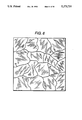
- FIG. 6 shows a top view through an optical microscope of columnar diamond crystals of the polycrystalline diamond film of the present invention.
- FIGS. 7 and 7a show the polycrystalline diamond film in cross section and in detail and the substantially transparent columns of diamond crystals having a ⁇ 110> orientation perpendicular to the bases.
- FIGS. 8 and 8a show apparatus for measuring the empirical transmittance of diamond film made in accordance with the practice of the present invention.
- FIGS. 9 and 9a are photos of the overall FIG. 8 set-up including an ammeter.
- FIGS. 9b and 9c are photos of an upper view and side view of the wedge shaped diamond film.
- FIGS. 10 and 11 are graphs showing transmittances of light through the diamond film wedge measured in photomultiplier tube current over a range of thickness of the diamond wedge.
- FIG. 1 is a schematic of a portion of an Hitachi 60 mm integrating sphere having an entrance and exit aperture and reference points for calibration.
- the integrating sphere is capable of measuring total transmitted light including I s and I u shown in formula (4) and reflected light, R, having both specular and diffused components, over the visible -NIR light range. It is used as an accessory in the Model U-3410 Recording Spectrophotometer of Hitachi Instruments Inc., Danbury, Conn.
- FIG. 1 shows a reflecting mirror at 10 for incident light, an entrance aperture at 11, an exit aperture at 12 and reference points at 13 and 14 for calibration.
- FIG. 1 also shows at the integrating sphere exit, a Spectralon Reflectance Calibration Standard from Lab Sphere Inc., North Sutton, N.H. This standard is used to calibrate the base line so that the intensity of incident light, I o , can be set at 100%.
- FIG. 2 shows the procedure for measuring the transmitted light I+I s through a 300 micron diamond film, from light transmitted at a wavelength in the range between about 300 to 2500 nm.
- the diamond film is secured to the entrance aperture of the integrating sphere.
- FIG. 3 shows the procedure used for directly measuring reflectance from a 300 micron diamond film at 30 using light over the range of about 300 nm to about 2500 nm.
- the diamond film is secured to an angular spacer at 31.
- FIG. 4 is a graph showing the absorbance corrected for both scatter and reflectance of a 300 micron diamond film made in accordance with the invention which resulted from the transmission of light over the range of about 300 nm to about 2500 nm.
- FIG. 5 shows a quartz bell jar having a metal flange which rests on a base. Inside the quartz bell jar, there is shown a support structure for a filament and several adjacent substrate sections.
- a quartz bell jar at 50 which can be 20"-30" tall and about 4"-6" wide having a metal collar at its base at 51 and a gas inlet at the top at 52.
- the metal collar portion rests on a rubber seal at 53 which can be Neoprene rubber.
- the rubber seal is supported by a metal base, such as steel base structure at 54 which has a vacuum opening at 55.
- the filament is secured by a screw at 61 to a metal plug at 62 which passes through a quartz insulating collar at 63 which is supported by an extension at 64. Electrical contacts are shown from the plug at 65 to a stud at 66 which is insulated from the metal base at 67.
- FIG. 6 showing a top view through an optical microscope of 10 to 200 micron columnar diamond crystals of the polycrystalline diamond film of the present invention separated by atomic grain boundaries such as shown at 30.
- FIG. 7 A further reference to the polycrystalline diamond film of the present invention is shown by FIG. 7.
- FIG. 7 A side view of the polycrystalline diamond film in cross section, and in detail which further illustrates the substantially transparent columns of diamond crystals having a ⁇ 110> orientation perpendicular to the base. Grain boundaries between adjacent diamond crystals having hydrogen atoms saturating dangling carbon bonds are shown at 40 and in detail at 41, where at least 50% of the carbon atoms are believed to be tetrahedrally bonded based on Raman spectroscopy, infrared and X-ray analysis.
- the above mechanism is one possible explanation as to how the transparent diamond film grows on the substrate.
- the polycrystalline diamond films made in accordance with the practice of the present invention can be used in a variety of glazing applications.
- the substantially transparent, free standing diamond film made in accordance with the practice of the invention having a thickness of at least 50 microns can have a thermal conductivity of at least about 4 W/cm-K and up to about 21 W/cm-K.
- Techniques which can be used to measure thermal conductivity of the substantially transparent diamond film are by Mirage, shown by R. W. Pryor et al., proceedings of the Second International Conference on New Diamond Science and Technology, p. 863 (1990).
- the diamond films can be employed as heat sinks or as semiconductors.
- the "empirical transmittance" of diamond film made in accordance with the practice of the present invention can be measured with the apparatus shown in FIG. 8 There is shown in FIG. 8, a laser at 80, a photomultiplier tube at 81, a diamond film in the form of a wedge at 82, a hidden view of the photomultiplier tube aperture at 83 note, FIG. 8a and a conductor at 84 for photomultiplier current connected to an ammeter not shown.
- the empirical transmittance is expressed in photomultiplier tube current. No allowance is made for light lost due to reflectance or scattering over various film thicknesses.
- the diamond wedge rests on a 4 mm diameter aperture in the photomultiplier tube (PMT).
- PMT photomultiplier tube
- FIG. 9 is a photo of the overall FIG. 8 set-up including an ammeter; FIGS. 9a shows a close up of the photomultiplier tube aperture and 9b and 9c show a top view and side view of the 12.5 mm square diamond wedge.
- FIG. 10 there is shown PMT current values expressed in terms of empirical transmittances (log 10 T 1 ) for three neutral density filters (0.1, 0.01 and 0.001) using light at 633 nm.
- FIG. 11 shows the plot of log 10 T 1 across the wedge surface of the substantially transparent diamond film made in accordance with the method of the invention.
- a gas flow rate of about 400 cubic centimeters per minute was maintained.
- the tungsten filament was maintained at a temperature between about 2020° to 2040° C.
- a separation of about 7-8 millimeters was maintained between the filament and the molybdenum substrate during the deposition which lasted approximately 30 days.
- the substrate temperature was estimated at about 800° C. during the deposition period.
- Substantially transparent polycrystalline diamond films having thicknesses of about 500 microns and lateral dimensions equivalent to the substrates separated from the substrate during the cooling period.
- the diamond films were found to be of good crystalline quality as shown by Raman spectra having an intense peak at 1332 cm -1 .
- the diamond films were also found to have the characteristic two phonon adsorption of material diamond in the range of 1600-2650 cm -1 by infrared spectroscopy.
- the diamond films were found to have a thermal conductivity of about 12 W/cm-K based on the Mirage technique previously cited.
- a mixture of 1.5 volume % of methane and 98.5 volume % of hydrogen measured under atmospheric conditions was introduced into a reaction vessel in accordance with example 1.
- a gas flow rate of 2.36 liters of hydrogen per minute and 36 cubic centimeters of methane per minute was maintained.
- There was used in the hot filament reactor 9 tungsten filaments 0.762 mm OD ⁇ 27.31 mm long.
- the tungsten filaments were employed 6.5 millimeters away from the molybdenum substrate.
- the filament temperature was 2015° C.
- the substrate temperature was 801° C.
- Substantially transparent polycrystalline diamond films having thicknesses of about 300 microns and lateral dimensions equivalent to the molybdenum substrates of Example 1 separated from the substrate during the cooling period.
- the diamond films were found to have a thermal conductivity of 4.4 to 4.6 W/cm-K.
- a 12 1/2 mm square section of the diamond film was then cut from the free-standing diamond film with a high powered laser.
- the apparent transmission of the above 12 1/2 mm square section of diamond film was then measured using an Hitachi 60 mm diameter integrating sphere accessory for the Model U-3410 Recording Spectrophotometer for visible-NIR measurements from Hitachi Instruments Inc. from Danbury, Conn.
- White calibration standards, Spectralon Reflectance Calibration Standard from Lab Sphere, Inc., North Sutton, N.H. were placed over the sphere exit and reference points in order to calibrate the base line, thereby setting the intensity of the incident light I o to 100%.
- the 12 1/2 mm square section of diamond film with the polished side facing the light source was then attached to the sphere entrance.
- the apparent transmission T A was then measured with the U-3410 spectrophotometer over a wavelength of 300 to 2500 nm.
- the apparent transmission included the light which was transmitted through the diamond film into the integrating sphere including the light which was scattered after it had passed through diamond film which was also captured by the integrating sphere. This measurement underestimated the true transmission because light reflected at film surfaces was not subtracted from the intensity of the incident beam.
- At least a partial correction for the reflected loss was made by measuring the light reflected from the front surface of the diamond film. In making this measurement, it was necessary to allow transmitted light to pass through the diamond film and out of the measurement area while reflected light is collected and measured.
- An angular spacer (C792456) for measuring specular reflectance was then placed at the sphere exit. This modification of the integrating sphere changed the optics to allow collection of both specular and diffused components of the scattered light.
- Calibration standards were then placed behind the spacer and at the reference point and the instrument was calibrated to a base line of 100%. The standard was then removed and the diamond film was placed and secured to the spacer over the exit of the sphere, with the polished surface of the film facing the sphere. The reflectance R was then measured. Reflectance was used to correct the apparent transmission using the following equation,
- % T can be converted to absorbance.
- the absorbance of the 300 micron diamond film was then plotted over a range of from about 300 nm to 2500 nm. The results are shown in FIG. 4.
- the 12 1/2 mm square diamond film section made in accordance with Example 2 was then formed into a wedge using an oblique mount, a conventional grinding apparatus composed of a large rotating metal disk which was continuously covered with an abrasive diamond/oil slurry.
- FIG. 10 shows the results of these calculations.
- FIG. 11 shows the empirical transmittance of the diamond wedge over various thicknesses. The results shown by FIGS.
Abstract
Description
______________________________________
CH.sub.4 (g) + □ = CH.sub.4 (ad)
                     (1)
CH.sub.4 (ad) = CH.sub.3 (ad) + H(ad)
                     (2)
CH.sub.3 (ad) = CH.sub.2 (ad) + H(ad)
                     (3)
CH.sub.2 (ad) = CH(ad) + H(ad)
                     (4)
CH(ad) = C(ad) + H(ad)
                     (5)
C(ad) = C(g) + □
                     (6)
CH(ad) = CH(g) + □
                     (7)
CH.sub.2 (ad) = CH.sub.2 (g) + □
                     (8)
CH.sub.3 (ad) = CH.sub.3 (g) + □
                     (9)
C(ad) = □ + C (in filament)
                     (10)
H.sub.2 (g) + 2□ = 2H(ad)
                     (11)
H(ad) = H(g) + □
                     (12)
______________________________________
 □ = vacant surface site
 (g) = gaseous species
 (ad) = species absorbed on surface
% T=T.sub.A 100/(100-R).
Claims (18)
Priority Applications (1)
| Application Number | Priority Date | Filing Date | Title |
|---|---|---|---|
| US07/859,753 US5273731A (en) | 1989-09-14 | 1992-03-30 | Substantially transparent free standing diamond films |
Applications Claiming Priority (2)
| Application Number | Priority Date | Filing Date | Title |
|---|---|---|---|
| US07/407,179 US5110579A (en) | 1989-09-14 | 1989-09-14 | Transparent diamond films and method for making |
| US07/859,753 US5273731A (en) | 1989-09-14 | 1992-03-30 | Substantially transparent free standing diamond films |
Related Parent Applications (1)
| Application Number | Title | Priority Date | Filing Date |
|---|---|---|---|
| US07/407,179 Continuation-In-Part US5110579A (en) | 1989-09-14 | 1989-09-14 | Transparent diamond films and method for making |
Publications (1)
| Publication Number | Publication Date |
|---|---|
| US5273731A true US5273731A (en) | 1993-12-28 |
Family
ID=27019791
Family Applications (1)
| Application Number | Title | Priority Date | Filing Date |
|---|---|---|---|
| US07/859,753 Expired - Lifetime US5273731A (en) | 1989-09-14 | 1992-03-30 | Substantially transparent free standing diamond films |
Country Status (1)
| Country | Link |
|---|---|
| US (1) | US5273731A (en) |
Cited By (43)
| Publication number | Priority date | Publication date | Assignee | Title |
|---|---|---|---|---|
| US5445106A (en) * | 1994-10-03 | 1995-08-29 | General Electric Company | Method for making high thermal conducting diamond |
| US5510098A (en) * | 1994-01-03 | 1996-04-23 | University Of Central Florida | CVD method of producing and doping fullerenes |
| US5525815A (en) * | 1994-10-03 | 1996-06-11 | General Electric Company | Diamond film structure with high thermal conductivity |
| US5554415A (en) | 1994-01-18 | 1996-09-10 | Qqc, Inc. | Substrate coating techniques, including fabricating materials on a surface of a substrate |
| US5556464A (en) * | 1992-07-15 | 1996-09-17 | Sumitomo Electric Industries, Ltd. | Vibration plate of a speaker and method for producing same |
| US5587013A (en) * | 1994-01-27 | 1996-12-24 | Sumitomo Electric Industries, Ltd. | Methods of synthesizing and polishing a flat diamond film and free-standing diamond film |
| EP0767394A1 (en) * | 1995-10-03 | 1997-04-09 | General Electric Company | Diamond optical plate beamsplitter |
| US5620754A (en) | 1994-01-21 | 1997-04-15 | Qqc, Inc. | Method of treating and coating substrates |
| US5634369A (en) * | 1995-07-07 | 1997-06-03 | General Electric Company | Composite diamond wire die |
| US5634370A (en) * | 1995-07-07 | 1997-06-03 | General Electric Company | Composite diamond wire die |
| US5636545A (en) * | 1995-07-07 | 1997-06-10 | General Electric Company | Composite diamond wire die |
| US5731046A (en) | 1994-01-18 | 1998-03-24 | Qqc, Inc. | Fabrication of diamond and diamond-like carbon coatings |
| US5736252A (en) * | 1993-01-22 | 1998-04-07 | Saint-Gobain/Norton Industrial Ceramics Corp. | Method of making white diamond film |
| US5736226A (en) * | 1994-06-09 | 1998-04-07 | Sumitomo Electric Industries, Ltd. | Wafer and method of producing a wafer |
| US5776246A (en) * | 1994-04-07 | 1998-07-07 | Sumitomo Electric Industries, Ltd. | Diamond wafer and method of producing a diamond wafer |
| US5792254A (en) * | 1996-06-12 | 1998-08-11 | Saint-Gobain/Norton Industrial Ceramics Corp. | Production of diamond film |
| US5855998A (en) * | 1994-05-23 | 1999-01-05 | Sumitomo Electric Industries, Ltd. | Hard material-coated wafer, method of making same, polishing apparatus and polishing method of hard material-coated wafer |
| US5874175A (en) * | 1988-11-29 | 1999-02-23 | Li; Chou H. | Ceramic composite |
| US6068070A (en) * | 1997-09-03 | 2000-05-30 | Baker Hughes Incorporated | Diamond enhanced bearing for earth-boring bit |
| US6209185B1 (en) | 1993-04-16 | 2001-04-03 | Baker Hughes Incorporated | Earth-boring bit with improved rigid face seal |
| US6286206B1 (en) | 1997-02-25 | 2001-09-11 | Chou H. Li | Heat-resistant electronic systems and circuit boards |
| US6384342B1 (en) | 1997-02-25 | 2002-05-07 | Chou H. Li | Heat-resistant electronic systems and circuit boards with heat resistant reinforcement dispersed in liquid metal |
| US6413589B1 (en) | 1988-11-29 | 2002-07-02 | Chou H. Li | Ceramic coating method |
| US6458017B1 (en) | 1998-12-15 | 2002-10-01 | Chou H. Li | Planarizing method |
| US20030077995A1 (en) * | 1998-07-09 | 2003-04-24 | Li Chou H. | Chemical mechanical polishing slurry |
| US6582513B1 (en) | 1998-05-15 | 2003-06-24 | Apollo Diamond, Inc. | System and method for producing synthetic diamond |
| US20030117706A1 (en) * | 2001-12-20 | 2003-06-26 | Sumitomo Electric Industries, Ltd. | Faraday rotator, optical isolator, polarizer, and diamond-like carbon thin film |
| US20030131787A1 (en) * | 1998-05-15 | 2003-07-17 | Linares Robert C. | Tunable CVD diamond structures |
| US6660342B1 (en) | 1990-09-25 | 2003-12-09 | Semiconductor Energy Laboratory Co., Ltd. | Pulsed electromagnetic energy method for forming a film |
| US6676492B2 (en) | 1998-12-15 | 2004-01-13 | Chou H. Li | Chemical mechanical polishing |
| US20040109328A1 (en) * | 2002-12-06 | 2004-06-10 | Chevron U.S.A. Inc. | Optical uses of diamondoid-containing materials |
| US20050019955A1 (en) * | 2003-07-23 | 2005-01-27 | Dahl Jeremy E. | Luminescent heterodiamondoids as biological labels |
| US20050181210A1 (en) * | 2004-02-13 | 2005-08-18 | Doering Patrick J. | Diamond structure separation |
| US20060261349A1 (en) * | 1998-05-15 | 2006-11-23 | Doering Patrick J | Single crystal diamond electrochemical electrode |
| EP2189555A2 (en) | 2001-08-08 | 2010-05-26 | Apollo Diamond, Inc. | System and method for producing synthetic diamond |
| CN103981511A (en) * | 2014-05-30 | 2014-08-13 | 大连理工常州研究院有限公司 | Vertically-arranged multi-array heating wire device for preparing diamond film |
| US8859058B2 (en) | 2010-12-23 | 2014-10-14 | Element Six Limited | Microwave plasma reactors and substrates for synthetic diamond manufacture |
| US8955456B2 (en) | 2010-12-23 | 2015-02-17 | Element Six Limited | Microwave plasma reactor for manufacturing synthetic diamond material |
| US9142389B2 (en) | 2010-12-23 | 2015-09-22 | Element Six Technologies Limited | Microwave power delivery system for plasma reactors |
| US9410242B2 (en) | 2010-12-23 | 2016-08-09 | Element Six Technologies Limited | Microwave plasma reactor for manufacturing synthetic diamond material |
| US9637838B2 (en) | 2010-12-23 | 2017-05-02 | Element Six Limited | Methods of manufacturing synthetic diamond material by microwave plasma enhanced chemical vapor deposition from a microwave generator and gas inlet(s) disposed opposite the growth surface area |
| US10403477B2 (en) | 2010-12-23 | 2019-09-03 | Element Six Technologies Limited | Microwave plasma reactor for manufacturing synthetic diamond material |
| US11371147B2 (en) | 2010-12-23 | 2022-06-28 | Element Six Technologies Limited | Microwave plasma reactor for manufacturing synthetic diamond material |
Citations (8)
| Publication number | Priority date | Publication date | Assignee | Title |
|---|---|---|---|---|
| US3030187A (en) * | 1958-07-23 | 1962-04-17 | Union Carbide Corp | Synthesis of diamond |
| US3630679A (en) * | 1968-06-26 | 1971-12-28 | Univ Case Western Reserve | Diamond growth process |
| US4767608A (en) * | 1986-10-23 | 1988-08-30 | National Institute For Research In Inorganic Materials | Method for synthesizing diamond by using plasma |
| US4816286A (en) * | 1985-11-25 | 1989-03-28 | Showa Denko Kabushiki Kaisha | Process for synthesis of diamond by CVD |
| US4830702A (en) * | 1987-07-02 | 1989-05-16 | General Electric Company | Hollow cathode plasma assisted apparatus and method of diamond synthesis |
| US4997636A (en) * | 1989-02-16 | 1991-03-05 | Prins Johan F | Diamond growth |
| US5106452A (en) * | 1989-06-05 | 1992-04-21 | Semiconductor Energy Laboratory Co., Ltd. | Method of depositing diamond and diamond light emitting device |
| US5110579A (en) * | 1989-09-14 | 1992-05-05 | General Electric Company | Transparent diamond films and method for making |
-
1992
- 1992-03-30 US US07/859,753 patent/US5273731A/en not_active Expired - Lifetime
Patent Citations (8)
| Publication number | Priority date | Publication date | Assignee | Title |
|---|---|---|---|---|
| US3030187A (en) * | 1958-07-23 | 1962-04-17 | Union Carbide Corp | Synthesis of diamond |
| US3630679A (en) * | 1968-06-26 | 1971-12-28 | Univ Case Western Reserve | Diamond growth process |
| US4816286A (en) * | 1985-11-25 | 1989-03-28 | Showa Denko Kabushiki Kaisha | Process for synthesis of diamond by CVD |
| US4767608A (en) * | 1986-10-23 | 1988-08-30 | National Institute For Research In Inorganic Materials | Method for synthesizing diamond by using plasma |
| US4830702A (en) * | 1987-07-02 | 1989-05-16 | General Electric Company | Hollow cathode plasma assisted apparatus and method of diamond synthesis |
| US4997636A (en) * | 1989-02-16 | 1991-03-05 | Prins Johan F | Diamond growth |
| US5106452A (en) * | 1989-06-05 | 1992-04-21 | Semiconductor Energy Laboratory Co., Ltd. | Method of depositing diamond and diamond light emitting device |
| US5110579A (en) * | 1989-09-14 | 1992-05-05 | General Electric Company | Transparent diamond films and method for making |
Non-Patent Citations (4)
| Title |
|---|
| Diamond Ceramic Coating of the Future, Karl E. Spear J. Am. Ceram. 1 Soc., 72 (2) 171 91 (1989) 4 random pages 171, 173, 186 and 187. * |
| Diamond-Ceramic Coating of the Future, Karl E. Spear-J. Am. Ceram. 1 Soc., 72 (2) 171-91 (1989) 4 random pages-171, 173, 186 and 187. |
| Unusually High Thermal Conductivity in Diamond Films, J. E. Graebner et al., Submitted to Applied Physics Letters (1991) pp. 1 10, plus Figures and Abstract. * |
| Unusually High Thermal Conductivity in Diamond Films, J. E. Graebner et al., Submitted to Applied Physics Letters (1991) pp. 1-10, plus Figures and Abstract. |
Cited By (83)
| Publication number | Priority date | Publication date | Assignee | Title |
|---|---|---|---|---|
| US6413589B1 (en) | 1988-11-29 | 2002-07-02 | Chou H. Li | Ceramic coating method |
| US5874175A (en) * | 1988-11-29 | 1999-02-23 | Li; Chou H. | Ceramic composite |
| US20040115365A1 (en) * | 1990-09-25 | 2004-06-17 | Semiconductor Energy Laboratory Co., Ltd. | Method for forming a film |
| US6660342B1 (en) | 1990-09-25 | 2003-12-09 | Semiconductor Energy Laboratory Co., Ltd. | Pulsed electromagnetic energy method for forming a film |
| US7125588B2 (en) | 1990-09-25 | 2006-10-24 | Semiconductor Energy Laboratory Co., Ltd. | Pulsed plasma CVD method for forming a film |
| US5556464A (en) * | 1992-07-15 | 1996-09-17 | Sumitomo Electric Industries, Ltd. | Vibration plate of a speaker and method for producing same |
| US5736252A (en) * | 1993-01-22 | 1998-04-07 | Saint-Gobain/Norton Industrial Ceramics Corp. | Method of making white diamond film |
| US6209185B1 (en) | 1993-04-16 | 2001-04-03 | Baker Hughes Incorporated | Earth-boring bit with improved rigid face seal |
| US5510098A (en) * | 1994-01-03 | 1996-04-23 | University Of Central Florida | CVD method of producing and doping fullerenes |
| US5731046A (en) | 1994-01-18 | 1998-03-24 | Qqc, Inc. | Fabrication of diamond and diamond-like carbon coatings |
| US5554415A (en) | 1994-01-18 | 1996-09-10 | Qqc, Inc. | Substrate coating techniques, including fabricating materials on a surface of a substrate |
| US5620754A (en) | 1994-01-21 | 1997-04-15 | Qqc, Inc. | Method of treating and coating substrates |
| US5587013A (en) * | 1994-01-27 | 1996-12-24 | Sumitomo Electric Industries, Ltd. | Methods of synthesizing and polishing a flat diamond film and free-standing diamond film |
| US6051063A (en) * | 1994-04-07 | 2000-04-18 | Sumitomo Electric Industries, Ltd. | Diamond wafer and method of producing a diamond wafer |
| US5776246A (en) * | 1994-04-07 | 1998-07-07 | Sumitomo Electric Industries, Ltd. | Diamond wafer and method of producing a diamond wafer |
| US6428399B1 (en) | 1994-05-23 | 2002-08-06 | Sumitomo Electric Industries, Ltd. | Polishing apparatus for polishing a hard material-coated wafer |
| US6193585B1 (en) | 1994-05-23 | 2001-02-27 | Sumitomo Electric Industries, Ltd. | Method of polishing a hard material-coated wafer |
| US5855998A (en) * | 1994-05-23 | 1999-01-05 | Sumitomo Electric Industries, Ltd. | Hard material-coated wafer, method of making same, polishing apparatus and polishing method of hard material-coated wafer |
| US5874130A (en) * | 1994-06-09 | 1999-02-23 | Sumitomo Electric Industries, Ltd. | Wafer and method of producing a wafer |
| US5736226A (en) * | 1994-06-09 | 1998-04-07 | Sumitomo Electric Industries, Ltd. | Wafer and method of producing a wafer |
| US5445106A (en) * | 1994-10-03 | 1995-08-29 | General Electric Company | Method for making high thermal conducting diamond |
| US5525815A (en) * | 1994-10-03 | 1996-06-11 | General Electric Company | Diamond film structure with high thermal conductivity |
| US5636545A (en) * | 1995-07-07 | 1997-06-10 | General Electric Company | Composite diamond wire die |
| US5634370A (en) * | 1995-07-07 | 1997-06-03 | General Electric Company | Composite diamond wire die |
| US5634369A (en) * | 1995-07-07 | 1997-06-03 | General Electric Company | Composite diamond wire die |
| US5706135A (en) * | 1995-10-03 | 1998-01-06 | General Electric Company | Diamond optical plate beamsplitter |
| EP0767394A1 (en) * | 1995-10-03 | 1997-04-09 | General Electric Company | Diamond optical plate beamsplitter |
| US5792254A (en) * | 1996-06-12 | 1998-08-11 | Saint-Gobain/Norton Industrial Ceramics Corp. | Production of diamond film |
| US6384342B1 (en) | 1997-02-25 | 2002-05-07 | Chou H. Li | Heat-resistant electronic systems and circuit boards with heat resistant reinforcement dispersed in liquid metal |
| US6938815B2 (en) | 1997-02-25 | 2005-09-06 | Chou H. Li | Heat-resistant electronic systems and circuit boards |
| US6286206B1 (en) | 1997-02-25 | 2001-09-11 | Chou H. Li | Heat-resistant electronic systems and circuit boards |
| US6068070A (en) * | 1997-09-03 | 2000-05-30 | Baker Hughes Incorporated | Diamond enhanced bearing for earth-boring bit |
| US20050056206A1 (en) * | 1998-05-15 | 2005-03-17 | Apollo Diamond, Inc. | Single crystal diamond having 12C, 13C, and phosphorous |
| US8187380B2 (en) | 1998-05-15 | 2012-05-29 | Apollo Diamond, Inc | Method of growing single crystal diamond in a plasma reactor |
| US20030131787A1 (en) * | 1998-05-15 | 2003-07-17 | Linares Robert C. | Tunable CVD diamond structures |
| US8974599B2 (en) | 1998-05-15 | 2015-03-10 | SCIO Diamond Technology Corporation | Boron doped single crystal diamond electrochemical synthesis electrode |
| US8591856B2 (en) | 1998-05-15 | 2013-11-26 | SCIO Diamond Technology Corporation | Single crystal diamond electrochemical electrode |
| US20030205190A1 (en) * | 1998-05-15 | 2003-11-06 | Linares Management Associates, Inc. | System and method for producing synthetic diamond |
| US7942966B2 (en) | 1998-05-15 | 2011-05-17 | Apollo Diamond, Inc. | Method of growing boron doped single crystal diamond in a plasma reactor |
| US7560086B2 (en) | 1998-05-15 | 2009-07-14 | Apollo Diamond, Inc. | Single crystal diamond having 12C, 13C, and phosphorous |
| US6858080B2 (en) | 1998-05-15 | 2005-02-22 | Apollo Diamond, Inc. | Tunable CVD diamond structures |
| US6582513B1 (en) | 1998-05-15 | 2003-06-24 | Apollo Diamond, Inc. | System and method for producing synthetic diamond |
| US20050056208A1 (en) * | 1998-05-15 | 2005-03-17 | Apollo Diamond, Inc. | Synthetic diamond having alternating layers with different concentrations of impurities |
| US20050056207A1 (en) * | 1998-05-15 | 2005-03-17 | Apollo Diamond, Inc. | Single crystal diamond tool |
| US20050056209A1 (en) * | 1998-05-15 | 2005-03-17 | Apollo Diamond, Inc. | Method of creating a synthetic diamond |
| US20050061233A1 (en) * | 1998-05-15 | 2005-03-24 | Apollo Diamond, Inc. | Method of forming an N-type doped single crystal diamond |
| US20050066884A1 (en) * | 1998-05-15 | 2005-03-31 | Apollo Diamond, Inc. | Method of growing a single crystal diamond |
| US20050085079A1 (en) * | 1998-05-15 | 2005-04-21 | Apollo Diamond, Inc. | Method of growing boron doped single crystal diamond in a plasma reactor |
| US20050109262A1 (en) * | 1998-05-15 | 2005-05-26 | Apollo Diamond, Inc. | Boron doped single crystal diamond electrochemical synthesis electrode |
| US20050109264A1 (en) * | 1998-05-15 | 2005-05-26 | Apollo Diamond, Inc. | Method of growing a single crystal diamond |
| US20050109265A1 (en) * | 1998-05-15 | 2005-05-26 | Apollo Diamond, Inc. | Single crystal synthetic diamond |
| US20050109268A1 (en) * | 1998-05-15 | 2005-05-26 | Apollo Diamond, Inc. | Single crystal diamond tool |
| US20050109267A1 (en) * | 1998-05-15 | 2005-05-26 | Apollo Diamond, Inc. | Method of growing single crystal diamond in a plasma reactor |
| US20050109266A1 (en) * | 1998-05-15 | 2005-05-26 | Apollo Diamond, Inc. | Arc jet microwave plasma method of growing single crystal diamond |
| US7459024B2 (en) | 1998-05-15 | 2008-12-02 | Apollo Diamond, Inc. | Method of forming an N-type doped single crystal diamond |
| US7258741B2 (en) | 1998-05-15 | 2007-08-21 | Apollo Diamond, Inc. | System and method for producing synthetic diamond |
| US7201886B2 (en) | 1998-05-15 | 2007-04-10 | Apollo Diamond, Inc. | Single crystal diamond tool |
| US20060261349A1 (en) * | 1998-05-15 | 2006-11-23 | Doering Patrick J | Single crystal diamond electrochemical electrode |
| US6976904B2 (en) | 1998-07-09 | 2005-12-20 | Li Family Holdings, Ltd. | Chemical mechanical polishing slurry |
| US20030077995A1 (en) * | 1998-07-09 | 2003-04-24 | Li Chou H. | Chemical mechanical polishing slurry |
| US6676492B2 (en) | 1998-12-15 | 2004-01-13 | Chou H. Li | Chemical mechanical polishing |
| US6458017B1 (en) | 1998-12-15 | 2002-10-01 | Chou H. Li | Planarizing method |
| EP2189555A2 (en) | 2001-08-08 | 2010-05-26 | Apollo Diamond, Inc. | System and method for producing synthetic diamond |
| US20030117706A1 (en) * | 2001-12-20 | 2003-06-26 | Sumitomo Electric Industries, Ltd. | Faraday rotator, optical isolator, polarizer, and diamond-like carbon thin film |
| US6813076B2 (en) * | 2001-12-20 | 2004-11-02 | Sumitomo Electric Industries, Ltd. | Faraday rotator, optical isolator, polarizer, and diamond-like carbon thin film |
| US20040109328A1 (en) * | 2002-12-06 | 2004-06-10 | Chevron U.S.A. Inc. | Optical uses of diamondoid-containing materials |
| US7224532B2 (en) | 2002-12-06 | 2007-05-29 | Chevron U.S.A. Inc. | Optical uses diamondoid-containing materials |
| US20080094724A1 (en) * | 2002-12-06 | 2008-04-24 | Chevron U.S.A. Inc. | Optical uses of diamondoid-containing materials |
| US20080094723A1 (en) * | 2002-12-06 | 2008-04-24 | Chevron U.S.A. Inc. | Optical uses of diamondoid-containing materials |
| US20080094722A1 (en) * | 2002-12-06 | 2008-04-24 | Chevron U.S.A. Inc. | Optical uses of diamondoid-containing materials |
| US20050019955A1 (en) * | 2003-07-23 | 2005-01-27 | Dahl Jeremy E. | Luminescent heterodiamondoids as biological labels |
| US20050181210A1 (en) * | 2004-02-13 | 2005-08-18 | Doering Patrick J. | Diamond structure separation |
| US9738970B2 (en) | 2010-12-23 | 2017-08-22 | Element Six Limited | Microwave plasma reactors and substrates for synthetic diamond manufacture |
| US8955456B2 (en) | 2010-12-23 | 2015-02-17 | Element Six Limited | Microwave plasma reactor for manufacturing synthetic diamond material |
| US8859058B2 (en) | 2010-12-23 | 2014-10-14 | Element Six Limited | Microwave plasma reactors and substrates for synthetic diamond manufacture |
| US9142389B2 (en) | 2010-12-23 | 2015-09-22 | Element Six Technologies Limited | Microwave power delivery system for plasma reactors |
| US9410242B2 (en) | 2010-12-23 | 2016-08-09 | Element Six Technologies Limited | Microwave plasma reactor for manufacturing synthetic diamond material |
| US9637838B2 (en) | 2010-12-23 | 2017-05-02 | Element Six Limited | Methods of manufacturing synthetic diamond material by microwave plasma enhanced chemical vapor deposition from a microwave generator and gas inlet(s) disposed opposite the growth surface area |
| US10403477B2 (en) | 2010-12-23 | 2019-09-03 | Element Six Technologies Limited | Microwave plasma reactor for manufacturing synthetic diamond material |
| US11371147B2 (en) | 2010-12-23 | 2022-06-28 | Element Six Technologies Limited | Microwave plasma reactor for manufacturing synthetic diamond material |
| US11488805B2 (en) | 2010-12-23 | 2022-11-01 | Element Six Technologies Limited | Microwave plasma reactor for manufacturing synthetic diamond material |
| CN103981511B (en) * | 2014-05-30 | 2016-06-29 | 大连理工常州研究院有限公司 | A kind of vertical arrangement prepares many array thermal silk device of diamond film |
| CN103981511A (en) * | 2014-05-30 | 2014-08-13 | 大连理工常州研究院有限公司 | Vertically-arranged multi-array heating wire device for preparing diamond film |
Similar Documents
| Publication | Publication Date | Title |
|---|---|---|
| US5273731A (en) | Substantially transparent free standing diamond films | |
| EP0676484B1 (en) | Transparent diamond films and method for making | |
| AU634601B2 (en) | Single-crystal diamond of very high thermal conductivity | |
| US5474021A (en) | Epitaxial growth of diamond from vapor phase | |
| US5127983A (en) | Method of producing single crystal of high-pressure phase material | |
| JP4768267B2 (en) | Optical quality diamond material | |
| US8974599B2 (en) | Boron doped single crystal diamond electrochemical synthesis electrode | |
| GB2433738A (en) | A CVD single crystal diamond material | |
| Wort et al. | Thermal properties of bulk polycrystalline CVD diamond | |
| US5310447A (en) | Single-crystal diamond of very high thermal conductivity | |
| IE911469A1 (en) | Radiation-Hard Optical Articles From Single-Crystal Diamond¹Of High Isotopic Purity | |
| Godet et al. | Characterization of microcrystallinity in hydrogenated silicon thin films | |
| Luk'yanov et al. | Measurement of optical absorption in polycrystalline CVD diamond plates by the phase photothermal method at a wavelength of 10.6 μm | |
| Lippold et al. | Raman and photoluminescence microscopy mapping of CVD micro-diamonds | |
| Zagoruiko et al. | Structure and physical properties of Zn 1-x Mg x Se single crystals | |
| Robinson et al. | Diamond for high heat flux applications | |
| Albin | Study of diamond film growth and properties | |
| Zwinge et al. | InP on Si substrates characterized by spectroscopic ellipsometry | |
| López‐Ríos et al. | Application of SERS to study chemical vapour deposition processes: the example of diamond films | |
| Yoo et al. | Growth of subgrain-free Tl3AsSe3 crystals for efficient harmonic conversion to mid-infrared frequency | |
| Shimada et al. | Raman scattering in low wavenumber region as a new probe to structural properties of microcrystalline silicon | |
| Obraztsov et al. | Raman spectrometer for in-situ study of diamond growth in DC discharge plasma CVD reactor | |
| Braunstein et al. | Infrared Wavelength Modulation Spectroscopy of Laser Window Materials | |
| Inoue et al. | DIRECT WRITING OF THIN FILMS BY PYROLYTIC LASER CVD | |
| Obraztsov et al. | Influence of structural characteristics on the thermal conductivity of polycrystalline diamond films |
Legal Events
| Date | Code | Title | Description |
|---|---|---|---|
| AS | Assignment |
Owner name: GENERAL ELECTRIC COMPANY, A NY CORP. Free format text: ASSIGNMENT OF ASSIGNORS INTEREST.;ASSIGNORS:ANTHONY, THOMAS R.;FLEISCHER, JAMES F.;REEL/FRAME:006070/0363 Effective date: 19920326 |
|
| FEPP | Fee payment procedure |
Free format text: PAYOR NUMBER ASSIGNED (ORIGINAL EVENT CODE: ASPN); ENTITY STATUS OF PATENT OWNER: LARGE ENTITY |
|
| STCF | Information on status: patent grant |
Free format text: PATENTED CASE |
|
| CC | Certificate of correction | ||
| FPAY | Fee payment |
Year of fee payment: 4 |
|
| FEPP | Fee payment procedure |
Free format text: PAYER NUMBER DE-ASSIGNED (ORIGINAL EVENT CODE: RMPN); ENTITY STATUS OF PATENT OWNER: LARGE ENTITY Free format text: PAYOR NUMBER ASSIGNED (ORIGINAL EVENT CODE: ASPN); ENTITY STATUS OF PATENT OWNER: LARGE ENTITY |
|
| FPAY | Fee payment |
Year of fee payment: 8 |
|
| AS | Assignment |
Owner name: DIAMOND INNOVATIONS, INC., OHIO Free format text: ASSIGNMENT OF ASSIGNORS INTEREST;ASSIGNOR:GE SUPERABRASIVES, INC.;REEL/FRAME:015147/0674 Effective date: 20031231 Owner name: GE SUPERABRASIVES, INC., CONNECTICUT Free format text: ASSIGNMENT OF ASSIGNORS INTEREST;ASSIGNOR:GENERAL ELECTRIC COMPANY;REEL/FRAME:015190/0560 Effective date: 20031231 |
|
| FPAY | Fee payment |
Year of fee payment: 12 |