US5301700A - Washing system - Google Patents
Washing system Download PDFInfo
- Publication number
- US5301700A US5301700A US08/026,771 US2677193A US5301700A US 5301700 A US5301700 A US 5301700A US 2677193 A US2677193 A US 2677193A US 5301700 A US5301700 A US 5301700A
- Authority
- US
- United States
- Prior art keywords
- washing
- section
- cassette
- cassettes
- wafers
- Prior art date
- Legal status (The legal status is an assumption and is not a legal conclusion. Google has not performed a legal analysis and makes no representation as to the accuracy of the status listed.)
- Expired - Lifetime
Links
Images


Classifications
-
- H—ELECTRICITY
- H01—ELECTRIC ELEMENTS
- H01L—SEMICONDUCTOR DEVICES NOT COVERED BY CLASS H10
- H01L21/00—Processes or apparatus adapted for the manufacture or treatment of semiconductor or solid state devices or of parts thereof
- H01L21/67—Apparatus specially adapted for handling semiconductor or electric solid state devices during manufacture or treatment thereof; Apparatus specially adapted for handling wafers during manufacture or treatment of semiconductor or electric solid state devices or components ; Apparatus not specifically provided for elsewhere
- H01L21/67005—Apparatus not specifically provided for elsewhere
- H01L21/67011—Apparatus for manufacture or treatment
- H01L21/67017—Apparatus for fluid treatment
- H01L21/67028—Apparatus for fluid treatment for cleaning followed by drying, rinsing, stripping, blasting or the like
- H01L21/6704—Apparatus for fluid treatment for cleaning followed by drying, rinsing, stripping, blasting or the like for wet cleaning or washing
- H01L21/67057—Apparatus for fluid treatment for cleaning followed by drying, rinsing, stripping, blasting or the like for wet cleaning or washing with the semiconductor substrates being dipped in baths or vessels
-
- B—PERFORMING OPERATIONS; TRANSPORTING
- B08—CLEANING
- B08B—CLEANING IN GENERAL; PREVENTION OF FOULING IN GENERAL
- B08B3/00—Cleaning by methods involving the use or presence of liquid or steam
- B08B3/02—Cleaning by the force of jets or sprays
- B08B3/022—Cleaning travelling work
-
- H—ELECTRICITY
- H01—ELECTRIC ELEMENTS
- H01L—SEMICONDUCTOR DEVICES NOT COVERED BY CLASS H10
- H01L21/00—Processes or apparatus adapted for the manufacture or treatment of semiconductor or solid state devices or of parts thereof
- H01L21/67—Apparatus specially adapted for handling semiconductor or electric solid state devices during manufacture or treatment thereof; Apparatus specially adapted for handling wafers during manufacture or treatment of semiconductor or electric solid state devices or components ; Apparatus not specifically provided for elsewhere
- H01L21/67005—Apparatus not specifically provided for elsewhere
- H01L21/67011—Apparatus for manufacture or treatment
- H01L21/67017—Apparatus for fluid treatment
- H01L21/67028—Apparatus for fluid treatment for cleaning followed by drying, rinsing, stripping, blasting or the like
- H01L21/6704—Apparatus for fluid treatment for cleaning followed by drying, rinsing, stripping, blasting or the like for wet cleaning or washing
- H01L21/67051—Apparatus for fluid treatment for cleaning followed by drying, rinsing, stripping, blasting or the like for wet cleaning or washing using mainly spraying means, e.g. nozzles
-
- H—ELECTRICITY
- H01—ELECTRIC ELEMENTS
- H01L—SEMICONDUCTOR DEVICES NOT COVERED BY CLASS H10
- H01L21/00—Processes or apparatus adapted for the manufacture or treatment of semiconductor or solid state devices or of parts thereof
- H01L21/67—Apparatus specially adapted for handling semiconductor or electric solid state devices during manufacture or treatment thereof; Apparatus specially adapted for handling wafers during manufacture or treatment of semiconductor or electric solid state devices or components ; Apparatus not specifically provided for elsewhere
- H01L21/677—Apparatus specially adapted for handling semiconductor or electric solid state devices during manufacture or treatment thereof; Apparatus specially adapted for handling wafers during manufacture or treatment of semiconductor or electric solid state devices or components ; Apparatus not specifically provided for elsewhere for conveying, e.g. between different workstations
- H01L21/67763—Apparatus specially adapted for handling semiconductor or electric solid state devices during manufacture or treatment thereof; Apparatus specially adapted for handling wafers during manufacture or treatment of semiconductor or electric solid state devices or components ; Apparatus not specifically provided for elsewhere for conveying, e.g. between different workstations the wafers being stored in a carrier, involving loading and unloading
- H01L21/67766—Mechanical parts of transfer devices
-
- H—ELECTRICITY
- H01—ELECTRIC ELEMENTS
- H01L—SEMICONDUCTOR DEVICES NOT COVERED BY CLASS H10
- H01L21/00—Processes or apparatus adapted for the manufacture or treatment of semiconductor or solid state devices or of parts thereof
- H01L21/67—Apparatus specially adapted for handling semiconductor or electric solid state devices during manufacture or treatment thereof; Apparatus specially adapted for handling wafers during manufacture or treatment of semiconductor or electric solid state devices or components ; Apparatus not specifically provided for elsewhere
- H01L21/677—Apparatus specially adapted for handling semiconductor or electric solid state devices during manufacture or treatment thereof; Apparatus specially adapted for handling wafers during manufacture or treatment of semiconductor or electric solid state devices or components ; Apparatus not specifically provided for elsewhere for conveying, e.g. between different workstations
- H01L21/67763—Apparatus specially adapted for handling semiconductor or electric solid state devices during manufacture or treatment thereof; Apparatus specially adapted for handling wafers during manufacture or treatment of semiconductor or electric solid state devices or components ; Apparatus not specifically provided for elsewhere for conveying, e.g. between different workstations the wafers being stored in a carrier, involving loading and unloading
- H01L21/67778—Apparatus specially adapted for handling semiconductor or electric solid state devices during manufacture or treatment thereof; Apparatus specially adapted for handling wafers during manufacture or treatment of semiconductor or electric solid state devices or components ; Apparatus not specifically provided for elsewhere for conveying, e.g. between different workstations the wafers being stored in a carrier, involving loading and unloading involving loading and unloading of wafers
- H01L21/67781—Batch transfer of wafers
-
- Y—GENERAL TAGGING OF NEW TECHNOLOGICAL DEVELOPMENTS; GENERAL TAGGING OF CROSS-SECTIONAL TECHNOLOGIES SPANNING OVER SEVERAL SECTIONS OF THE IPC; TECHNICAL SUBJECTS COVERED BY FORMER USPC CROSS-REFERENCE ART COLLECTIONS [XRACs] AND DIGESTS
- Y10—TECHNICAL SUBJECTS COVERED BY FORMER USPC
- Y10S—TECHNICAL SUBJECTS COVERED BY FORMER USPC CROSS-REFERENCE ART COLLECTIONS [XRACs] AND DIGESTS
- Y10S134/00—Cleaning and liquid contact with solids
- Y10S134/902—Semiconductor wafer
-
- Y—GENERAL TAGGING OF NEW TECHNOLOGICAL DEVELOPMENTS; GENERAL TAGGING OF CROSS-SECTIONAL TECHNOLOGIES SPANNING OVER SEVERAL SECTIONS OF THE IPC; TECHNICAL SUBJECTS COVERED BY FORMER USPC CROSS-REFERENCE ART COLLECTIONS [XRACs] AND DIGESTS
- Y10—TECHNICAL SUBJECTS COVERED BY FORMER USPC
- Y10S—TECHNICAL SUBJECTS COVERED BY FORMER USPC CROSS-REFERENCE ART COLLECTIONS [XRACs] AND DIGESTS
- Y10S414/00—Material or article handling
- Y10S414/135—Associated with semiconductor wafer handling
- Y10S414/137—Associated with semiconductor wafer handling including means for charging or discharging wafer cassette
- Y10S414/138—Wafers positioned vertically within cassette
-
- Y—GENERAL TAGGING OF NEW TECHNOLOGICAL DEVELOPMENTS; GENERAL TAGGING OF CROSS-SECTIONAL TECHNOLOGIES SPANNING OVER SEVERAL SECTIONS OF THE IPC; TECHNICAL SUBJECTS COVERED BY FORMER USPC CROSS-REFERENCE ART COLLECTIONS [XRACs] AND DIGESTS
- Y10—TECHNICAL SUBJECTS COVERED BY FORMER USPC
- Y10S—TECHNICAL SUBJECTS COVERED BY FORMER USPC CROSS-REFERENCE ART COLLECTIONS [XRACs] AND DIGESTS
- Y10S414/00—Material or article handling
- Y10S414/135—Associated with semiconductor wafer handling
- Y10S414/14—Wafer cassette transporting
Definitions
- the present invention relates to a washing system for washing semiconductor wafers and wafer cassettes.
- semiconductor devices such as super LSIs have been more and more highly integrated and their circuit patterns have been micro-structured to an order of submicrons.
- the diameter of semiconductor wafers has been made large to 8 inches and even 12 inches. When such a small amount of particles that could be hitherto neglected adhere to semiconductor wafers, therefore, the productivity of wafers is remarkably lowered.
- the semiconductor wafers are immersed into acid and alkali solutions in process vessels so that their surfaces can be made clean.
- the automatic washing system can be cited as a system for washing the surface of each wafer. It has plural process vessels in which the semiconductor wafers are washed by chemical solutions and water and then dried. Namely, an ammonium solution vessel, a water-washing vessel, a rinsing vessel, a hydrofluoric acid vessel and a drying chamber are arranged in it to enable a series of processes to be sequentially applied to the semiconductor wafers.
- the wafer cassette has a plurality of grooves in which wafers are seated, and the whole of the cassette is thus made complicated in shape. This makes it difficult to remove acid and alkali solutions from the cassette.
- material e.g. an ethylene fluoride system resin
- the cassette is repeatedly immersed in acid and alkali solutions, material (e.g. an ethylene fluoride system resin) of which the cassette is made solves little by little into the chemical solutions to degrade them in the process vessels.
- the wafers are taken out of the cassette and are immersed and washed in the chemical solutions.
- the wafers which have been thus made clean are then returned into their original cassette.
- the object of the present invention is therefore to provide a washing system capable of preventing dust, particles and contaminating objects adhered to a cassette from transferring to a semiconductor wafer and also capable of preventing dust and particles caused at drive mechanisms of conveying units from transferring to a wafer.
- a washing system comprising a wafer washing section having means for washing plural semiconductor wafers by chemical solution, means for washing the wafers by water and means for drying the wafer; a cassette washing section having means for washing plural cassettes by water and means for drying the wafers; a loader section for taking out the wafers from the cassette and for loading the wafers into the wafer washing section; an unloader section for returning the wafers in the washed cassette and unloading the washed wafers from the wafer washing section; means for carrying the wafers in the wafer washing section; and means for carrying the cassettes from the loader section to the cassette washing section.
- the wafers are washed in the wafer washing section while the cassettes in the cassette washing section. This enables the washed wafers to be returned into the washed cassette to thereby prevent contamination such as particles from transferring from the cassettes to the wafers.
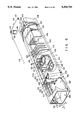
- FIG. 1 is a perspective view showing the whole of the washing system according to an embodiment of the present invention
- FIG. 2 is a perspective view showing a wafer carrier mechanism provided with input and output buffer sections of the washing system
- FIG. 3 is a perspective view showing a cassette stocking unit
- FIGS. 4A and 4B schematically show wafer lifter and chuck
- FIG. 5 is a perspective view showing a cassette lifter
- FIG. 6 is a perspective view showing a cassette washing passage partly cut
- FIG. 7 is a perspective view showing a wafer carrier mechanism at the washing section
- FIG. 8 is a perspective view partly showing a drive section of the wafer carrier mechanism at the washing section
- FIG. 9 is a perspective view showing chuck arms of the wafer carrier mechanism at the washing section and a wafer boat in a chemical solution vessel;
- FIG. 10 schematically shows the drive section and a shield belt at the wafer carrier mechanism
- FIG. 11 is a perspective view showing the drive section for a wafer chuck at the wafer carrier mechanism
- FIG. 12 is a perspective view showing a safety mechanism for the wafer chuck
- FIG. 13 is a perspective view showing another wafer carrier mechanism of the washing section partly cut;
- FIG. 14 is a perspective view showing chuck arms of a further wafer carrier mechanism and a wafer boat in the chemical solution vessel at the washing section;
- FIGS. 15A through 15C show how chuck arms of a still further wafer carrier mechanism are operated at the washing section.
- FIG. 16 is a perspective view showing a shutter interposed between the chemical solution vessels.
- a washing system 1 comprises three sections, that is, a washing section 2 and input and output buffer sections 3 and 4.
- the input buffer section 3 is located on the side of a loader section 5 and the output buffer section 4 on the side of an unloader section 6.
- the washing section 2 includes a lower area for washing semiconductor wafers and an upper area for washing wafer cassettes. Both of a passage 100 in the cassettes washing area are communicated with the input and output buffer sections 3 and 4.
- the input and output buffer sections 3 and 4 are substantially same in structure. Description will be made, therefore, on the input buffer section 3 but not on the output buffer section 4.
- Two cassettes C are received on a port 14 at the input buffer section 3. 25 sheets of 8-inch (or 6-inch or 5-inch) silicon wafers W are housed in each of the cassettes C.
- Two cassette carrier units 12 are opposed to the port 14. These two cassette carrier units 12 are mounted on turntables 31.
- the cassette carrier unit 12 is located between the port 14 and a cassette stocking unit 13. It has two pairs of chucks 300 at its front end.
- the chucks 300 are made of resin such as PEEK or PVC. They are supported by an X-axis mover 301, a Y-axis mover 302 and the ⁇ -direction rotator (or turn-table) 31. They are also supported by a Z-axis mover 307.
- the drive part of the X-axis mover 301 is sealed by a seal belt 303, that of the Y-axis mover 302 by a seal belt 305, and that of the Z-axis mover 307 by a bellows seal 304.
- These seal belts 303, 305 and bellows seal 304 are made of ethylene tetrafluoride resin. Exhausts (not shown) are connected to these components.
- the cassette stocking unit 13 includes therein four compartments 200 piled like steps in the vertical direction. Two cassettes C are housed in each of these four compartments 200.
- the compartments 200 are supported by an elevator unit 202 in which a ball screw drive mechanism is housed.
- the elevator unit 202 moves the compartments 200 up and down at a speed of 5 mm-70 mm/sec. It is enclosed by a cylindrical cover 203.
- An exhaust pipe 207 is connected to the lower end of the cover 203.
- the compartments 200 and the elevator unit 202 are housed in a box-like case 204.
- a filter unit 205 having a filter (or ULPA filter, for example) for removing dust and particles, and fans 206 are arranged on the top of the case 204. Openings 201 are formed in the bottom of each of the compartments 200 to allow clean air to flow, as a down flow, from up to down through them.
- the case 204 has an opening 208 through which the cassettes C are carried in and out of the case 204.
- a wafers lifter 60 is arranged under a turntable 32 at the loader section 5.
- the cassettes C are mounted on the table 32 in such a way that their openings are aligned with an opening 32a of the table 32.
- a member 62 of the wafers lifter 60 is arranged to come into and out of the opening 32a of the table 32. 25 grooves are formed on the top of the member 62 and when a rod 61 is projected from a lift cylinder (not shown), wafers are held an the grooves of the member 62. Needless to say, another same wafers lifter 60 is arranged at the unloader section 6.
- a wafer chuck 50 moves from a washing vessel 7a to the loader section 5 to receive the wafers W from the lifter 60.
- the loader section 5 is provided with an aligning device (not shown) for aligning orientation flats of the wafers W with one another and with a wafer counter (not shown) for detecting the number of the wafers W.
- the loader and unloader sections 5 and 6 are located on both sides of the washing section 2 and seven vessels 7a-7i are arranged side by side on a line between these sections 5 and 6.
- the wafers W can be thus successively washed and cleaned while moving from the vessel 7a to the one 7i.
- the vessels 7a and 7h are intended to wash and dry the wafers chuck 50
- the vessels 7b and 7e contain chemical solutions
- the vessels 7c, 7d, 7f and 7g are intended to wash the wafers W and the vessel 7i to dry them.
- These vessels 7a-7i are housed in their corresponding chambers 18a-18i, which are partitioned by opening-provided shutters or partition plates (not shown).
- Each of the wafers carrier units 8 has the wafer chuck 50, by which fifty sheets of wafers a, maximum, can be held together.
- a switching window made by a transparent acrylic plate is attached to the front aide of the washing section 2 and the vessels 7a-7i can be viewed from outside through the window.
- the passage 100 in which the cassettes C are washed while passing through it is arranged in the upper portion of the washing section 2.
- a plurality of exhaust pipes are arranged in the lower portion of it.
- a plurality of tanks in which chemical solutions and pure water are contained are also arranged in the rear portion of it.
- a lifter 70 is arranged in it to lift the cassettes C from the loader section 5 into the passage 10.
- Another same cassette lifter 70 is also arranged in the unloader section 6.
- the cassette lifter 70 has two fingers 77, by which two cassettes are lifted at the same time.
- a Z-axis mover 72 for the cassette lifter 70 is fixed to a support 71 and supported by it.
- the Z-axis mover 72 includes a motor 80 and a ball screw 81.
- Ball nuts (not shown) are attached to the rear side of a moving base 74 and they are toothed with the ball screw 81.
- the moving base 74 is supported, balancing a balance 82, and guided along a linear motion bearing 73.
- An X-axis mover 75 is attached to the underside of the moving base 74. Further, a ⁇ -direction rotator 76 is attached to the underside of the X-axis mover 75.
- the two fingers 77 extend horizontal from the ⁇ -direction rotator 76. Base end portions of these two fingers 77 are bent like cranks. When the fingers 77 are swung along the axis ⁇ by the ⁇ -axis rotator 76, they obliquely advance approach to the cassettes C from above position, while drawing arc-like curves, and they embrace them under their collars. In other words, the cassettes C are hung from the fingers 77 by their collars.
- the cassette washing passage 100 will be now described, referring to FIGS. 1 and 6.
- the passage 100 is made substantially air-tight at its main portion and its both open ends are communicated with the loader and unloader sections 5 and 6.
- the main portion of the passage 100 extends straight along the front side of the system 1, that is, along the axis X.
- the switching window made of transparent acryl is fitted in the wall by which the main portion of the passage 100 is enclosed, and the cassettes C in the passage 100 can be viewed from outside through the window.
- the passage 100 includes therein a cassettes carrying-in section 101, a water-washing section 102, a gas-jetting section 103, a heat-drying section 104 and a cassettes carrying-out section 105.
- Plural moving stages 110 are arranged in the passage 100.
- Two cassettes C are mounted on each of the moving stages 110.
- a slider 112a is attached to the front end of an arm 112 of the moving stage 110 and it is slid relative to a rail unit 113 while being guided along a slit 121 of a guide 120.
- a wire 114 extends in the rail unit 113 and drive force is added to the slider 112a of the moving stage 110 by the wire 114.
- each of pulley 115 is provided in a corner of the line of the wire 114, respectively.
- One of pulley 115 is rotated by a motor 116 which has a reduction gears. It is made of stainless steel and coated with ethylene tetrafluoride resin.
- a shutter 106 is interposed between the carrying-in section 101 and the water-washing section 102.
- the shutter 106 is of the accordion curtain type, having a rail wheel 108 and a slide rail 109, and it is opened and closed by a cylinder 107.
- Three spray pipes 130 are arranged side by side in the water-washing section 102. Each of the spray pipes 130 has a plurality of nozzles 131 and it is shaped like a fallen U.
- the moving stage 110 is formed with drain openings 111 and the water-washing section 102 has a drain opening 124 in the bottom thereof and a gas exhaust opening 125 in a side wall thereof.
- the rail unit 113 and the guide 120 are protected from water by a water-proof plate 122.
- a partition plate 119 is interposed between the water-washing section 102 and the gas-jetting section 103.
- the cassettes C on the moving stage 110 pass through an opening of the partition plate 119.
- Three gas-jetting pipes 132 are arranged side by side in the gas-jetting section 103.
- Each of the gas-jetting pipes 132 is shaped like a fallen U and when the cassettes C on the moving stage 110 are passed through the U-shaped pipes 132, dry nitrogen gas is jetted from three directions against the cassettes C through nozzles of the pipes 132.
- Two heating units 134 and 135 are arranged in the heat-drying section 104.
- Plural far-infrared heaters 136 are arranged on the inner face of each of the heating units 134 and 135.
- a switching shutter 108 is located on the outlet side of the heat-drying section 10a.
- the inner face of each of the heating units 13a and 135 is made by an SiO 2 plate coated with tantalum to have a high reflection rate.
- the wafer carrier mechanism or unit will be now described with reference to FIGS. 7 through 11.
- the wafer carrier unit 8 has the wafer chuck 50 made of quartz or PEEK, by which fifty sheets of wafers W are held.
- a carrying base 51 is arranged along the line of the process vessels 7a-7i.
- the wafer chuck 50 is attached to a chuck base 52 movable along the X- and Z-axis.
- the X-axis drive section of the carrying base 51 is sealed by a teflon-made seal belt 53, the Z-axis drive section thereof by a bellows seal 54 and the Y-axis drive section of the chuck base 52 by bellows seals 55 to seal their mechanical drive parts.
- the X-axis drive mechanism of the chuck base 52 is of the rack pinion type, comprising a motor 500, a pinion 501 attached to a drive shaft of the motor 500. and a rack 502 of the carrying base 51 engaged with the pinion 501.
- a wafer boat 700 is arranged in each of the process vessels 7a-7i.
- the wafer chuck 50 is moved along the Y-axis by the chuck base 52.
- This movement of the wafer chuck 50 along the Y-axis is intended to correct that position of the wafer chuck 50 relative to the wafer boat 700 where wafers W are transferred from the wafer chuck 50 into the wafer boat 700.
- the wafer boat 700 as not always stopped correctly relative to the carrying base 51 or sometimes stopped, positionally shifting from the carrying base 51. Therefore, this positional shift of the wafer boat 700 can be corrected by moving the wafer chuck 50 along the Y-axis.
- the extent to which the wafer chuck 50 must be moved along the Y-axis to correct its wafers-transferring position in relation to the wafer boat 700 is previously determined every process vessel by initial adjustment and the values thus obtained are stored in the memory of a drive control unit (not shown).
- a drive control unit not shown.
- Both ends of the wafer boat 700 are supported by position adjusters 701.
- the position of the wafer boat 700 can be micro-adjusted by three height-adjusting bolts 702 and fixing bolts 703. When it is adjusted from outside the process vessels 7a-7i in this manner, it can be made unnecessary for the operator to put his hands into any of the process vessels for the positional adjustment of the wafer boat 700.
- the seal belt 53 is stretched round four guide rolls 510 which are located around the motor 500. Each of the guide rolls 510 is supported rotatable such that it is driven through the belt 53 by the motor 500.
- the seal belt 53 is not moved in this case but the motor 500 is moved along the X-axis by a rack 501 and a pinion 502.
- the seal belt 53 serves to prevent particles caused by the working drive parts from being scattered through that opening of the moving base 51 which is sealed by the seal belt 53.
- the wafer chuck 50 has a Y-axis drive motor 56, to the drive shaft of which a ball screw 57 is connected.
- the ball screw 57 is screwed into a ball nut 58 attached to the chuck base 52.
- the motor 56 is rotated, the wafer chuck 50 is moved along the Y-axis.
- a coil spring 60 is attached to the rear end of the chuck 50 to urge the chuck 50 to be closed.
- This coil spring serves as a safety member. Even if power is accidentally stopped while the wafers W are being carried in the chuck 50, therefore, the wafers W can be prevented from falling out of the chuck 50 by the coil spring 60.
- another type wafer carrier mechanism or unit 800 may be used.
- the chuck base 52 is supported by two pipe-shaped members 801 of double pipe structure each being made by covering an iron-made pipe with a resin-made pipe.
- a Z-axis mover 802 is housed in a Z-axis mover case 803 to move the chuck base 52 up and down along the Z-axis.
- a seal packing 804 is attached to the top of the case 803 and the pipe-shaped members 801 pass through the top of the case 803, a little contacting the seal packing 804.
- This wafer carrier unit 800 can prevent, without using the bellows seal 54, dust and particles caused by the Z-axis mover 802 and the like from being scattered outside and chemical solution from entering into the Z-axis mover 802.
- a wafer chuck 612 includes a pair of right and left arms 618R and 618L whose upper ends are crossed and freely rotatably connected each other, and an arms opening and closing means 619.
- the wafers holding arms 618R and 618L are gently curved in such a direction that they are closed and particularly their lower halves are curved at same curvature as the outer circumference of each wafer.
- Rod-like wafer holder members 620 and 621 extend horizontal and parallel from each of the wafers holding arms 618R and 618L Grooves 620a and 621a in which the wafers W are seated are formed on the wafer holder members 620 and 621.
- Front ends of the lower and upper wafer holder members 620 and 621 extending from each of the wafers holding arms 618R and 618L are connected each other by an end plate 622, which serves to reinforce the wafer holder members 620 and 621 and prevent the wafers W from falling out of the wafer holder members 620 and 621.
- the arms opening and closing means 619 is hinged to the upper ends of the arms 618R and 618L.
- a link member 625 and an arm lifter 626 cooperate with the wafers holding arms 618R and 618L to form a pantograph mechanism 624.
- a cover member 627 covers the pantograph mechanism 624.
- a spring 628 is provided between right and left hinged portion of the pantograph mechanism 624.
- the pantograph mechanism 624 is pushed open (or pressed downward) by the spring 628.
- the arm lifter 626 includes a rod 630 and a support 631.
- the rod 630 is arranged to move up and down along a vertical slit 629 in the front face of a block 617.
- a drive means (not shown) comprising a motor, gears and links is housed in the block 617.
- the support 631 is fixed to the front end of the rod 630 and a hinged portion 625a of the link member 625 is pivoted on the support 631.
- the cover member 627 is tapered, spreading wider as it comes nearer to its lower end. Both sides of the cover member 627 are curved outward to form guide grooves 627a and both right and left ends of the pantograph section 624 are slidably contacted with inner faces of these guide grooves 627a of the cover member 627.
- the process of washing the wafers W will be carried out as follows: As shown in FIG. 15A, the wafer chuck 612 by which the wafers W not processed yet are held is moved into a process vessel 609 to mount the wafers W on wafers-mounted members 623. The retreat of the wafer chuck 612 out of the process vessel 609 is conducted opening and closing the wafers holding arms 618R and 618L along the outer circumference of the wafers a.
- the right and left arms 618a and 618L of the wafer chuck 612 are opened until their lower wafer holder members 620 can have an interval a little larger than the diameter of each wafer W.
- the block 617 is then moved upward to pull the wafer chuck 612 out of the process vessel 609.
- a washing liquid 635 is supplied from a supply source (not shown) into the process vessel 609 and the wafers W are washed in it.
- the washing liquid may be stored in the process vessel 609. The wafers W are immersed into the washing liquid and then washed in this case.
- a shutter unit serving as a partition between the adjacent ones of process chambers 18a-18i will be described referring to FIG. 16.
- a shutter unit 920 has a water-absorbing film sheet 922 wound round a drum 921.
- the film sheet 922 is dropped by lifters 928 and 934 to shut the opening through which both adjacent process chambers are communicated with each other.
- Nozzles 923 are located above and under the drum 921 and when water is sprayed to the film sheet 922 through these nozzles 923, water curtains 929 are created on both sides of the film sheet 922.
- a water-receiving tray 924 made of vinyl chloride is arranged under the iower end of the film sheet 922 in this case.
- a movable element 925 made of vinyl chloride and attached to one end of the water-receiving tray 924 is made slidable alona a guide rail 927 which is also made of vinyl chloride and fixed vertical to a side wall 926 of the process chamber 18.
- the film sheet 922 is made by cloth or corrosion-proof fibers such as teflon. Or it is made by putting corrosion-proof fibers and films one over another.
- the bottom of the water-receiving tray 924 is tilted to one end and a drain pipe 930 is connected to a drain hole (not shown) in this bottom end of the tray 924. Water sprayed through the nozzles 923 and dropped along the film sheet 922 can be therefore drained outside through the drain pipe 930.
- Two cassettes C are mounted in the boat 14 at the input buffer section 3 by a robot (not shown). Twenty sheets of 8-inch silicon wafers W are housed in each of the cassettes C. Orientation flats of the semiconductor wafers W in each of the cassettes C in the boat 14 are aligned with one another by the aligning unit (not shown).
- the cassettes C are carried to the loader section 5 by the cassette carrier unit 12. However, they are housed in the cassettes stocking unit 13 when other cassettes are already present in the loader section 5.
- the wafers W in the cassettes C are lifted in the loader section 5 and held together, total fifty sheets, by the chuck 50 of the carrier unit 8. They are then carried into the second process chamber 18b. While being successively carried in this manner by the three carrier units 8, they are processed by chemical solution, water, water, chemical solution, water, water and finally dried in the chambers 18b-18i. When they are dried by heat, they are carried to the unloader section 6. Those cassettes C which have washed clean are waiting in the unloader section 6. The wafers W are housed in these two clean cassettes C and carried to the output buffer section 4 and then outside from the boat 14.
- the cassettes C which have been made vacant in the loader section 5 are lifted to the cassettes washing passage 100 and mounted on the moving stage 110 by the lifter 70.
- the number of the cassettes mounted in this case may be one or two.
- wafers W may be housed in the cassettes C.
- the carrying of the cassettes C in the passage 100 by wire drive is made intermittent. Namely, it is stopped when the cassettes C are transferred onto the moving stage 110, when the shutters 106 of the water washing chamber 102 and heat drying chamber 104 are opened and closed, and when the cassettes C are being water-washed and heat-dried.
- the cassettes C which have been made clean are carried from the passage 100 to the unloader section 6 and mounted on the table 32 by the lifter 70.
- the wafers W which have also been made clean are then housed in the clean cassettes C by the carrier unit 8 and the lifter 60.
- the whole time needed to process the cassettes C in a cycle, while carrying them from the loader 5 to the unloader section 6, is about 5 minutes, shortest.
- the process of washing the cassettes C can be carried out together with the process of washing the wafers W. This can make the working efficiency and the through-put quite higher.
- the wafers W which have been made clean are returned into the clean cassettes C. This can prevent particles from adhering to the wafers.
- the productivity of semiconductor devices can be enhanced.
Abstract
Description
Claims (12)
Applications Claiming Priority (8)
| Application Number | Priority Date | Filing Date | Title |
|---|---|---|---|
| JP4083216A JPH05251414A (en) | 1992-03-05 | 1992-03-05 | Cleaning equipment |
| JP4-83216 | 1992-03-05 | ||
| JP4-62083 | 1992-03-18 | ||
| JP6208392 | 1992-03-18 | ||
| JP4-96073 | 1992-03-24 | ||
| JP9607392A JPH05270660A (en) | 1992-03-24 | 1992-03-24 | Cleaning treatment |
| JP04249252A JP3113411B2 (en) | 1992-03-18 | 1992-09-18 | Cleaning equipment |
| JP4-249252 | 1992-09-18 |
Publications (1)
| Publication Number | Publication Date |
|---|---|
| US5301700A true US5301700A (en) | 1994-04-12 |
Family
ID=27464121
Family Applications (1)
| Application Number | Title | Priority Date | Filing Date |
|---|---|---|---|
| US08/026,771 Expired - Lifetime US5301700A (en) | 1992-03-05 | 1993-03-05 | Washing system |
Country Status (1)
| Country | Link |
|---|---|
| US (1) | US5301700A (en) |
Cited By (59)
| Publication number | Priority date | Publication date | Assignee | Title |
|---|---|---|---|---|
| US5370142A (en) * | 1992-11-10 | 1994-12-06 | Tokyo Electron Limited | Substrate washing device |
| US5445171A (en) * | 1992-09-25 | 1995-08-29 | Mitsubishi Denki Kabushiki Kaisha | Semiconductor cleaning apparatus and wafer cassette |
| WO1995030238A1 (en) * | 1994-04-28 | 1995-11-09 | Semitool, Inc. | Semiconductor wafer processing system |
| GB2291740A (en) * | 1994-07-22 | 1996-01-31 | Nec Corp | Wet processing system wafer transport apparatus |
| WO1996021241A1 (en) * | 1995-01-05 | 1996-07-11 | Steag Microtech Gmbh | Wet chemical treatment installation |
| US5603777A (en) * | 1994-06-27 | 1997-02-18 | Dainippon Screen Mfg. Co., Ltd. | Substrate surface treating apparatus and substrate surface treating method |
| US5664337A (en) * | 1996-03-26 | 1997-09-09 | Semitool, Inc. | Automated semiconductor processing systems |
| US5731678A (en) * | 1996-07-15 | 1998-03-24 | Semitool, Inc. | Processing head for semiconductor processing machines |
| US5784802A (en) * | 1994-04-28 | 1998-07-28 | Semitool, Inc. | Semiconductor processing systems |
| US5784797A (en) * | 1994-04-28 | 1998-07-28 | Semitool, Inc. | Carrierless centrifugal semiconductor processing system |
| US5825470A (en) * | 1995-03-14 | 1998-10-20 | Nikon Corporation | Exposure apparatus |
| US5836736A (en) * | 1994-04-28 | 1998-11-17 | Semitool, Inc. | Semiconductor processing system with wafer container docking and loading station |
| US5853496A (en) * | 1995-08-08 | 1998-12-29 | Tokyo Electron Limited | Transfer machine, transfer method, cleaning machine, and cleaning method |
| US6039057A (en) * | 1993-03-05 | 2000-03-21 | Hyundai Electronics America | Automated washing system and method |
| WO2000038221A1 (en) * | 1998-12-22 | 2000-06-29 | Steag Microtech Gmbh | Device for processing substrates |
| US6091498A (en) * | 1996-07-15 | 2000-07-18 | Semitool, Inc. | Semiconductor processing apparatus having lift and tilt mechanism |
| US6203582B1 (en) | 1996-07-15 | 2001-03-20 | Semitool, Inc. | Modular semiconductor workpiece processing tool |
| US6267123B1 (en) * | 1998-03-23 | 2001-07-31 | Kabushiki Kaisha Toshiba | Pod and method of cleaning it |
| WO2002005316A2 (en) * | 2000-07-07 | 2002-01-17 | Fluoroware, Inc. | Wafer container washing apparatus |
| US6354794B2 (en) * | 1998-11-03 | 2002-03-12 | Seh America, Inc. | Method for automatically transferring wafers between wafer holders in a liquid environment |
| US20020084183A1 (en) * | 2000-03-21 | 2002-07-04 | Hanson Kyle M. | Apparatus and method for electrochemically processing a microelectronic workpiece |
| US20020100495A1 (en) * | 1998-07-10 | 2002-08-01 | Semitool, Inc. | Method and apparatus for cleaning containers |
| US20020139678A1 (en) * | 1999-04-13 | 2002-10-03 | Wilson Gregory J. | Tuning electrodes used in a reactor for electrochemically processing a microelectronic workpiece |
| WO2003006183A2 (en) * | 2001-07-12 | 2003-01-23 | Semitool, Inc. | Method and apparatus for cleaning semiconductor wafers and other flat media |
| US20030102015A1 (en) * | 1998-01-09 | 2003-06-05 | Halbmaier David L. | Wafer container washing apparatus |
| US6576065B1 (en) * | 1998-03-09 | 2003-06-10 | S.O.I.Tech Silicon On Insulator Technologies | Installation and method for chemical treatment of microelectronics wafers |
| US6579056B2 (en) * | 2000-06-02 | 2003-06-17 | Tokyo Electron Limited | Cart for mounting/demounting wafer transfer robot |
| US20030131874A1 (en) * | 1994-04-28 | 2003-07-17 | Davis Jeffrey A. | Automated semiconductor processing systems |
| US6645355B2 (en) | 1996-07-15 | 2003-11-11 | Semitool, Inc. | Semiconductor processing apparatus having lift and tilt mechanism |
| US20030209404A1 (en) * | 2000-07-07 | 2003-11-13 | Davis Jeffry A. | Automated processing system |
| US6651704B2 (en) * | 2001-11-19 | 2003-11-25 | Taiwan Semiconductor Manufacturing Co., Ltd | Stationary and pivotable trays for semiconductor wafer transfer |
| WO2003105192A2 (en) * | 2002-06-07 | 2003-12-18 | Akrion, Llc | Apparatus and method for cassette-less transfer of wafers |
| US6672820B1 (en) | 1996-07-15 | 2004-01-06 | Semitool, Inc. | Semiconductor processing apparatus having linear conveyer system |
| US6691718B2 (en) * | 1999-07-28 | 2004-02-17 | Semitool, Inc. | Wafer container cleaning system |
| US20040031693A1 (en) * | 1998-03-20 | 2004-02-19 | Chen Linlin | Apparatus and method for electrochemically depositing metal on a semiconductor workpiece |
| US20040049911A1 (en) * | 2002-07-16 | 2004-03-18 | Harris Randy A. | Apparatuses and method for transferring and/or pre-processing microelectronic workpieces |
| US6723174B2 (en) | 1996-03-26 | 2004-04-20 | Semitool, Inc. | Automated semiconductor processing system |
| US20040084066A1 (en) * | 2002-11-01 | 2004-05-06 | Semitool, Inc. | Wafer container cleaning system |
| US20040108212A1 (en) * | 2002-12-06 | 2004-06-10 | Lyndon Graham | Apparatus and methods for transferring heat during chemical processing of microelectronic workpieces |
| US6797076B1 (en) | 1998-07-10 | 2004-09-28 | Semitool, Inc. | Spray nozzle system for a semiconductor wafer container cleaning aparatus |
| US6833035B1 (en) | 1994-04-28 | 2004-12-21 | Semitool, Inc. | Semiconductor processing system with wafer container docking and loading station |
| US20050084987A1 (en) * | 1999-07-12 | 2005-04-21 | Wilson Gregory J. | Tuning electrodes used in a reactor for electrochemically processing a microelectronic workpiece |
| US20050087439A1 (en) * | 1999-04-13 | 2005-04-28 | Hanson Kyle M. | Chambers, systems, and methods for electrochemically processing microfeature workpieces |
| US20050109612A1 (en) * | 1998-07-10 | 2005-05-26 | Woodruff Daniel J. | Electroplating apparatus with segmented anode array |
| US20050139478A1 (en) * | 1998-03-20 | 2005-06-30 | Semitool, Inc. | Apparatus and method for electrolytically depositing copper on a semiconductor workpiece |
| US6942738B1 (en) * | 1996-07-15 | 2005-09-13 | Semitool, Inc. | Automated semiconductor processing system |
| US7021323B1 (en) * | 2000-06-01 | 2006-04-04 | Dainichi Shoji Kabushiki Kaisha | Dust-incompatible article transfer container cleaner |
| US20060144325A1 (en) * | 2005-01-05 | 2006-07-06 | Samsung Sdi Co., Ltd. | Driving shaft of effusion cell for deposition system and deposition system having the same |
| US7160421B2 (en) | 1999-04-13 | 2007-01-09 | Semitool, Inc. | Turning electrodes used in a reactor for electrochemically processing a microelectronic workpiece |
| US20070079932A1 (en) * | 2001-12-07 | 2007-04-12 | Applied Materials, Inc. | Directed purge for contact free drying of wafers |
| US20070092635A1 (en) * | 2005-10-21 | 2007-04-26 | Huh Myung S | Apparatus and method for depositing thin films |
| DE10039672B4 (en) * | 1999-08-13 | 2007-07-12 | Tokyo Electron Ltd. | Substrate processing apparatus and method of processing a substrate |
| CN1327978C (en) * | 2003-12-05 | 2007-07-25 | 华联生物科技股份有限公司 | Combined cleaning rack and its rack body |
| US20090067960A1 (en) * | 2007-09-12 | 2009-03-12 | Samsung Electronics Co., Ltd. | Wafer guide for preventing wafer breakage in semiconductor cleaning apparatus |
| US20090084416A1 (en) * | 2007-09-28 | 2009-04-02 | Siltron Inc. | Box cleaner for cleaning wafer shipping box |
| US20120046781A1 (en) * | 2004-07-02 | 2012-02-23 | Strasbaugh, A California Corporation | Method, apparatus and system for use in processing wafers |
| US20120325272A1 (en) * | 2011-06-23 | 2012-12-27 | Dynamic Micro Systems, Semiconductor Equipment Gmbh | Semiconductor cleaner systems and methods |
| US20160225649A1 (en) * | 2015-01-29 | 2016-08-04 | Taiwan Semiconductor Manufacturing Co., Ltd. | Load port and method for loading and unloading cassette |
| CN112735999A (en) * | 2020-12-30 | 2021-04-30 | 上海至纯洁净系统科技股份有限公司 | Universal wafer transfer mechanism and transfer method thereof |
Citations (4)
| Publication number | Priority date | Publication date | Assignee | Title |
|---|---|---|---|---|
| US4437479A (en) * | 1981-12-30 | 1984-03-20 | Atcor | Decontamination apparatus for semiconductor wafer handling equipment |
| JPS60231337A (en) * | 1984-04-27 | 1985-11-16 | Fujitsu Ltd | Wafer transfer device |
| JPS6412534A (en) * | 1987-07-06 | 1989-01-17 | Mitsubishi Electric Corp | Wafer cassette purification device |
| US4941489A (en) * | 1987-05-06 | 1990-07-17 | Dan Science Co., Ltd. | Carrier cleaning and drying apparatus |
-
1993
- 1993-03-05 US US08/026,771 patent/US5301700A/en not_active Expired - Lifetime
Patent Citations (4)
| Publication number | Priority date | Publication date | Assignee | Title |
|---|---|---|---|---|
| US4437479A (en) * | 1981-12-30 | 1984-03-20 | Atcor | Decontamination apparatus for semiconductor wafer handling equipment |
| JPS60231337A (en) * | 1984-04-27 | 1985-11-16 | Fujitsu Ltd | Wafer transfer device |
| US4941489A (en) * | 1987-05-06 | 1990-07-17 | Dan Science Co., Ltd. | Carrier cleaning and drying apparatus |
| JPS6412534A (en) * | 1987-07-06 | 1989-01-17 | Mitsubishi Electric Corp | Wafer cassette purification device |
Non-Patent Citations (2)
| Title |
|---|
| Patent Abstracts of Japan, Apr. 7, 1992, Y. Kushima, "Cover Mechanism for Movable Zone." |
| Patent Abstracts of Japan, Apr. 7, 1992, Y. Kushima, Cover Mechanism for Movable Zone. * |
Cited By (119)
| Publication number | Priority date | Publication date | Assignee | Title |
|---|---|---|---|---|
| US5551459A (en) * | 1992-09-25 | 1996-09-03 | Mitsubishi Denki Kabushiki Kaisha | Semiconductor cleaning apparatus and wafer cassette |
| US5445171A (en) * | 1992-09-25 | 1995-08-29 | Mitsubishi Denki Kabushiki Kaisha | Semiconductor cleaning apparatus and wafer cassette |
| US5590672A (en) * | 1992-09-25 | 1997-01-07 | Mitsubishi Denki Kabushiki Kaisha | Semiconductor cleaning apparatus and wafer cassette |
| US5568821A (en) * | 1992-09-25 | 1996-10-29 | Mitsubishi Denki Kabushiki Kaisha | Semiconductor cleaning apparatus and wafer cassette |
| US5370142A (en) * | 1992-11-10 | 1994-12-06 | Tokyo Electron Limited | Substrate washing device |
| US6039057A (en) * | 1993-03-05 | 2000-03-21 | Hyundai Electronics America | Automated washing system and method |
| US5788454A (en) * | 1994-04-28 | 1998-08-04 | Semitool, Inc. | Semiconductor wafer processing system |
| US5882168A (en) * | 1994-04-28 | 1999-03-16 | Semitool, Inc. | Semiconductor processing systems |
| US6712577B2 (en) * | 1994-04-28 | 2004-03-30 | Semitool, Inc. | Automated semiconductor processing system |
| US6833035B1 (en) | 1994-04-28 | 2004-12-21 | Semitool, Inc. | Semiconductor processing system with wafer container docking and loading station |
| US5660517A (en) * | 1994-04-28 | 1997-08-26 | Semitool, Inc. | Semiconductor processing system with wafer container docking and loading station |
| US20050045214A1 (en) * | 1994-04-28 | 2005-03-03 | Semitool, Inc. | Automated semiconductor processing systems |
| US5678320A (en) * | 1994-04-28 | 1997-10-21 | Semitool, Inc. | Semiconductor processing systems |
| US7080652B2 (en) | 1994-04-28 | 2006-07-25 | Semitool, Inc. | Automated semiconductor processing systems |
| US5784802A (en) * | 1994-04-28 | 1998-07-28 | Semitool, Inc. | Semiconductor processing systems |
| US5784797A (en) * | 1994-04-28 | 1998-07-28 | Semitool, Inc. | Carrierless centrifugal semiconductor processing system |
| US20030131874A1 (en) * | 1994-04-28 | 2003-07-17 | Davis Jeffrey A. | Automated semiconductor processing systems |
| WO1995030238A1 (en) * | 1994-04-28 | 1995-11-09 | Semitool, Inc. | Semiconductor wafer processing system |
| US6871655B2 (en) | 1994-04-28 | 2005-03-29 | Semitool, Inc. | Automated semiconductor processing systems |
| US5836736A (en) * | 1994-04-28 | 1998-11-17 | Semitool, Inc. | Semiconductor processing system with wafer container docking and loading station |
| US6960257B2 (en) | 1994-04-28 | 2005-11-01 | Semitool, Inc. | Semiconductor processing system with wafer container docking and loading station |
| US5544421A (en) * | 1994-04-28 | 1996-08-13 | Semitool, Inc. | Semiconductor wafer processing system |
| US6014817A (en) * | 1994-04-28 | 2000-01-18 | Semitool, Inc. | Semiconductor wafer processing system |
| US5996241A (en) * | 1994-04-28 | 1999-12-07 | Semitool, Inc. | Semiconductor wafer processing system with immersion module |
| US5603777A (en) * | 1994-06-27 | 1997-02-18 | Dainippon Screen Mfg. Co., Ltd. | Substrate surface treating apparatus and substrate surface treating method |
| GB2291740A (en) * | 1994-07-22 | 1996-01-31 | Nec Corp | Wet processing system wafer transport apparatus |
| US6099686A (en) * | 1994-07-22 | 2000-08-08 | Nec Corporation | Wet processing system |
| GB2291740B (en) * | 1994-07-22 | 1998-08-19 | Nec Corp | Wet processing system |
| US5902402A (en) * | 1995-01-05 | 1999-05-11 | Steag Microtech Gmbh | Device for chemical wet treatment |
| WO1996021241A1 (en) * | 1995-01-05 | 1996-07-11 | Steag Microtech Gmbh | Wet chemical treatment installation |
| CN1084048C (en) * | 1995-01-05 | 2002-05-01 | 施蒂格微技术有限公司 | Wet chemical treatment installation |
| US5825470A (en) * | 1995-03-14 | 1998-10-20 | Nikon Corporation | Exposure apparatus |
| US5853496A (en) * | 1995-08-08 | 1998-12-29 | Tokyo Electron Limited | Transfer machine, transfer method, cleaning machine, and cleaning method |
| US5664337A (en) * | 1996-03-26 | 1997-09-09 | Semitool, Inc. | Automated semiconductor processing systems |
| US6723174B2 (en) | 1996-03-26 | 2004-04-20 | Semitool, Inc. | Automated semiconductor processing system |
| US6203582B1 (en) | 1996-07-15 | 2001-03-20 | Semitool, Inc. | Modular semiconductor workpiece processing tool |
| US6645355B2 (en) | 1996-07-15 | 2003-11-11 | Semitool, Inc. | Semiconductor processing apparatus having lift and tilt mechanism |
| US5731678A (en) * | 1996-07-15 | 1998-03-24 | Semitool, Inc. | Processing head for semiconductor processing machines |
| US6440178B2 (en) | 1996-07-15 | 2002-08-27 | Semitool, Inc. | Modular semiconductor workpiece processing tool |
| US7002698B2 (en) | 1996-07-15 | 2006-02-21 | Semitool, Inc. | Semiconductor processing apparatus having lift and tilt mechanism |
| US6091498A (en) * | 1996-07-15 | 2000-07-18 | Semitool, Inc. | Semiconductor processing apparatus having lift and tilt mechanism |
| US6942738B1 (en) * | 1996-07-15 | 2005-09-13 | Semitool, Inc. | Automated semiconductor processing system |
| US20050193537A1 (en) * | 1996-07-15 | 2005-09-08 | Berner Robert W. | Modular semiconductor workpiece processing tool |
| US7074246B2 (en) | 1996-07-15 | 2006-07-11 | Semitool, Inc. | Modular semiconductor workpiece processing tool |
| US6672820B1 (en) | 1996-07-15 | 2004-01-06 | Semitool, Inc. | Semiconductor processing apparatus having linear conveyer system |
| US6654122B1 (en) | 1996-07-15 | 2003-11-25 | Semitool, Inc. | Semiconductor processing apparatus having lift and tilt mechanism |
| US20040226510A1 (en) * | 1996-07-15 | 2004-11-18 | Semitool. Inc. | Semiconductor processing apparatus having lift and tilt mechanism |
| US6926017B2 (en) | 1998-01-09 | 2005-08-09 | Entegris, Inc. | Wafer container washing apparatus |
| US20030102015A1 (en) * | 1998-01-09 | 2003-06-05 | Halbmaier David L. | Wafer container washing apparatus |
| US7216655B2 (en) | 1998-01-09 | 2007-05-15 | Entegris, Inc. | Wafer container washing apparatus |
| US6576065B1 (en) * | 1998-03-09 | 2003-06-10 | S.O.I.Tech Silicon On Insulator Technologies | Installation and method for chemical treatment of microelectronics wafers |
| US20050150770A1 (en) * | 1998-03-20 | 2005-07-14 | Semitool, Inc. | Apparatus and method for electrolytically depositing copper on a semiconductor workpiece |
| US20050173252A1 (en) * | 1998-03-20 | 2005-08-11 | Semitool, Inc. | Apparatus and method for electrolytically depositing copper on a semiconductor workpiece |
| US20050139478A1 (en) * | 1998-03-20 | 2005-06-30 | Semitool, Inc. | Apparatus and method for electrolytically depositing copper on a semiconductor workpiece |
| US20100116671A1 (en) * | 1998-03-20 | 2010-05-13 | Semitool, Inc. | Apparatus and method for electrochemically depositing metal on a semiconductor workpiece |
| US20040031693A1 (en) * | 1998-03-20 | 2004-02-19 | Chen Linlin | Apparatus and method for electrochemically depositing metal on a semiconductor workpiece |
| US20050245083A1 (en) * | 1998-03-20 | 2005-11-03 | Semitool, Inc. | Apparatus and method for electrochemically depositing metal on a semiconductor workpiece |
| US6422247B2 (en) | 1998-03-23 | 2002-07-23 | Kabushiki Kaisha Toshiba | Pod and method of cleaning it |
| US6267123B1 (en) * | 1998-03-23 | 2001-07-31 | Kabushiki Kaisha Toshiba | Pod and method of cleaning it |
| US20050109611A1 (en) * | 1998-07-10 | 2005-05-26 | Woodruff Daniel J. | Electroplating apparatus with segmented anode array |
| US20050109612A1 (en) * | 1998-07-10 | 2005-05-26 | Woodruff Daniel J. | Electroplating apparatus with segmented anode array |
| US6797076B1 (en) | 1998-07-10 | 2004-09-28 | Semitool, Inc. | Spray nozzle system for a semiconductor wafer container cleaning aparatus |
| US20050268944A1 (en) * | 1998-07-10 | 2005-12-08 | Dan Bexten | Method and apparatus for cleaning containers |
| US20020100495A1 (en) * | 1998-07-10 | 2002-08-01 | Semitool, Inc. | Method and apparatus for cleaning containers |
| US6904920B2 (en) * | 1998-07-10 | 2005-06-14 | Semitool, Inc. | Method and apparatus for cleaning containers |
| US6354794B2 (en) * | 1998-11-03 | 2002-03-12 | Seh America, Inc. | Method for automatically transferring wafers between wafer holders in a liquid environment |
| US6457929B2 (en) * | 1998-11-03 | 2002-10-01 | Seh America, Inc. | Apparatus and method for automatically transferring wafers between wafer holders in a liquid environment |
| WO2000038221A1 (en) * | 1998-12-22 | 2000-06-29 | Steag Microtech Gmbh | Device for processing substrates |
| US20090114533A9 (en) * | 1999-04-13 | 2009-05-07 | Hanson Kyle M | Chambers, systems, and methods for electrochemically processing microfeature workpieces |
| US20050087439A1 (en) * | 1999-04-13 | 2005-04-28 | Hanson Kyle M. | Chambers, systems, and methods for electrochemically processing microfeature workpieces |
| US20020139678A1 (en) * | 1999-04-13 | 2002-10-03 | Wilson Gregory J. | Tuning electrodes used in a reactor for electrochemically processing a microelectronic workpiece |
| US7160421B2 (en) | 1999-04-13 | 2007-01-09 | Semitool, Inc. | Turning electrodes used in a reactor for electrochemically processing a microelectronic workpiece |
| US20040188259A1 (en) * | 1999-04-13 | 2004-09-30 | Wilson Gregory J. | Tuning electrodes used in a reactor for electrochemically processing a microelectronic workpiece |
| US20050084987A1 (en) * | 1999-07-12 | 2005-04-21 | Wilson Gregory J. | Tuning electrodes used in a reactor for electrochemically processing a microelectronic workpiece |
| US6691718B2 (en) * | 1999-07-28 | 2004-02-17 | Semitool, Inc. | Wafer container cleaning system |
| DE10039672B4 (en) * | 1999-08-13 | 2007-07-12 | Tokyo Electron Ltd. | Substrate processing apparatus and method of processing a substrate |
| US20020084183A1 (en) * | 2000-03-21 | 2002-07-04 | Hanson Kyle M. | Apparatus and method for electrochemically processing a microelectronic workpiece |
| US7021323B1 (en) * | 2000-06-01 | 2006-04-04 | Dainichi Shoji Kabushiki Kaisha | Dust-incompatible article transfer container cleaner |
| US6579056B2 (en) * | 2000-06-02 | 2003-06-17 | Tokyo Electron Limited | Cart for mounting/demounting wafer transfer robot |
| WO2002005316A2 (en) * | 2000-07-07 | 2002-01-17 | Fluoroware, Inc. | Wafer container washing apparatus |
| US20030209404A1 (en) * | 2000-07-07 | 2003-11-13 | Davis Jeffry A. | Automated processing system |
| WO2002005316A3 (en) * | 2000-07-07 | 2002-04-04 | Fluoroware Inc | Wafer container washing apparatus |
| US7278813B2 (en) | 2000-07-07 | 2007-10-09 | Semitool, Inc. | Automated processing system |
| WO2003006183A3 (en) * | 2001-07-12 | 2003-02-27 | Semitool Inc | Method and apparatus for cleaning semiconductor wafers and other flat media |
| WO2003006183A2 (en) * | 2001-07-12 | 2003-01-23 | Semitool, Inc. | Method and apparatus for cleaning semiconductor wafers and other flat media |
| US6651704B2 (en) * | 2001-11-19 | 2003-11-25 | Taiwan Semiconductor Manufacturing Co., Ltd | Stationary and pivotable trays for semiconductor wafer transfer |
| US20070079932A1 (en) * | 2001-12-07 | 2007-04-12 | Applied Materials, Inc. | Directed purge for contact free drying of wafers |
| WO2003105192A3 (en) * | 2002-06-07 | 2004-03-18 | Akrion Llc | Apparatus and method for cassette-less transfer of wafers |
| WO2003105192A2 (en) * | 2002-06-07 | 2003-12-18 | Akrion, Llc | Apparatus and method for cassette-less transfer of wafers |
| US7114903B2 (en) | 2002-07-16 | 2006-10-03 | Semitool, Inc. | Apparatuses and method for transferring and/or pre-processing microelectronic workpieces |
| US20040049911A1 (en) * | 2002-07-16 | 2004-03-18 | Harris Randy A. | Apparatuses and method for transferring and/or pre-processing microelectronic workpieces |
| US20040084066A1 (en) * | 2002-11-01 | 2004-05-06 | Semitool, Inc. | Wafer container cleaning system |
| US7060138B2 (en) | 2002-11-01 | 2006-06-13 | Semitool, Inc. | Methods for cleaning wafer containers |
| US20050011540A1 (en) * | 2002-11-01 | 2005-01-20 | Semitool, Inc. | Wafer container cleaning system |
| US6830057B2 (en) | 2002-11-01 | 2004-12-14 | Semitool, Inc. | Wafer container cleaning system |
| US20040108212A1 (en) * | 2002-12-06 | 2004-06-10 | Lyndon Graham | Apparatus and methods for transferring heat during chemical processing of microelectronic workpieces |
| CN1327978C (en) * | 2003-12-05 | 2007-07-25 | 华联生物科技股份有限公司 | Combined cleaning rack and its rack body |
| US8565919B2 (en) * | 2004-07-02 | 2013-10-22 | Strasbaugh | Method, apparatus and system for use in processing wafers |
| US20120046781A1 (en) * | 2004-07-02 | 2012-02-23 | Strasbaugh, A California Corporation | Method, apparatus and system for use in processing wafers |
| US8366832B2 (en) * | 2005-01-05 | 2013-02-05 | Samsung Displays Co., Ltd. | Driving shaft of effusion cell for deposition system and deposition system having the same |
| US20060144325A1 (en) * | 2005-01-05 | 2006-07-06 | Samsung Sdi Co., Ltd. | Driving shaft of effusion cell for deposition system and deposition system having the same |
| US20070092635A1 (en) * | 2005-10-21 | 2007-04-26 | Huh Myung S | Apparatus and method for depositing thin films |
| US8033401B2 (en) | 2007-09-12 | 2011-10-11 | Samsung Electronics Co., Ltd. | Wafer guide for preventing wafer breakage in semiconductor cleaning apparatus |
| US20090067960A1 (en) * | 2007-09-12 | 2009-03-12 | Samsung Electronics Co., Ltd. | Wafer guide for preventing wafer breakage in semiconductor cleaning apparatus |
| KR101231182B1 (en) | 2007-09-12 | 2013-02-07 | 삼성전자주식회사 | Waferguide for preventing wafer broken of semiconductor cleaning equipment |
| US7976642B2 (en) * | 2007-09-28 | 2011-07-12 | Siltron, Inc. | Box cleaner for cleaning wafer shipping box |
| US20090084416A1 (en) * | 2007-09-28 | 2009-04-02 | Siltron Inc. | Box cleaner for cleaning wafer shipping box |
| US20180330940A1 (en) * | 2011-06-23 | 2018-11-15 | Brooks Automation Gmbh | Semiconductor cleaner systems and methods |
| US9646858B2 (en) | 2011-06-23 | 2017-05-09 | Brooks Automation, Inc. | Semiconductor cleaner systems and methods |
| US9646817B2 (en) | 2011-06-23 | 2017-05-09 | Brooks Automation, Inc. | Semiconductor cleaner systems and methods |
| US10026604B2 (en) | 2011-06-23 | 2018-07-17 | Brooks Automation (Germany) Gmbh | Semiconductor cleaner systems and methods |
| US10043651B2 (en) | 2011-06-23 | 2018-08-07 | Brooks Automation (Germany) Gmbh | Semiconductor cleaner systems and methods |
| US10096461B2 (en) * | 2011-06-23 | 2018-10-09 | Brooks Automation Germany, GmbH | Semiconductor cleaner systems and methods |
| US20120325272A1 (en) * | 2011-06-23 | 2012-12-27 | Dynamic Micro Systems, Semiconductor Equipment Gmbh | Semiconductor cleaner systems and methods |
| US10892155B2 (en) * | 2011-06-23 | 2021-01-12 | Brooks Automation (Germany) Gmbh | Semiconductor cleaner systems and methods |
| US11152203B2 (en) | 2011-06-23 | 2021-10-19 | Brooks Automation (Germany) Gmbh | Semiconductor cleaner systems and methods |
| US20160225649A1 (en) * | 2015-01-29 | 2016-08-04 | Taiwan Semiconductor Manufacturing Co., Ltd. | Load port and method for loading and unloading cassette |
| US9852936B2 (en) * | 2015-01-29 | 2017-12-26 | Taiwan Semiconductor Manufacturing Co., Ltd. | Load port and method for loading and unloading cassette |
| CN112735999A (en) * | 2020-12-30 | 2021-04-30 | 上海至纯洁净系统科技股份有限公司 | Universal wafer transfer mechanism and transfer method thereof |
Similar Documents
| Publication | Publication Date | Title |
|---|---|---|
| US5301700A (en) | Washing system | |
| US6874515B2 (en) | Substrate dual-side processing apparatus | |
| KR101798320B1 (en) | Substrate processing apparatus | |
| US5327921A (en) | Processing vessel for a wafer washing system | |
| US6374837B2 (en) | Single semiconductor wafer processor | |
| JP5841389B2 (en) | Substrate processing apparatus and substrate processing method | |
| US6799586B2 (en) | Substrate processing method | |
| EP0753884A2 (en) | Apparatus and method for washing treatment | |
| KR101901012B1 (en) | Substrate processing apparatus | |
| US20080041422A1 (en) | Semiconductor substrate cleaning system | |
| CN108803257B (en) | Liquid supply unit, substrate processing apparatus, and substrate processing method | |
| KR20080009660A (en) | Substrate processing apparatus | |
| KR101052818B1 (en) | Maintenance method in substrate processing apparatus and substrate processing apparatus | |
| KR20030071649A (en) | Liquid processing apparatus and liquid processing method | |
| US6668844B2 (en) | Systems and methods for processing workpieces | |
| KR101747083B1 (en) | Auto modified surface inspection system of wafer | |
| KR102366179B1 (en) | Transger unit and apparatus for treating substrate with the transfer unit | |
| JP3908916B2 (en) | Substrate processing equipment | |
| KR102522960B1 (en) | Apparatus for treating substrate | |
| KR102121241B1 (en) | Apparatus for treating substrate | |
| KR102616521B1 (en) | Substrate processing apparatus, treatment solution supply apparatus and treatment solution supply method | |
| KR0163361B1 (en) | Cleaning apparatus | |
| JP3857655B2 (en) | Substrate processing equipment | |
| KR102010261B1 (en) | Apparatus and Method for treating a substrate | |
| KR101817213B1 (en) | Apparatus for treating substrate |
Legal Events
| Date | Code | Title | Description |
|---|---|---|---|
| AS | Assignment |
Owner name: TOKYO ELECTRON LIMITED, JAPAN Free format text: ASSIGNMENT OF ASSIGNORS INTEREST;ASSIGNORS:KAMIKAWA, YUUJI;KURODA, KOUKI;HONDA, YOSHIYUKI;AND OTHERS;REEL/FRAME:006540/0743 Effective date: 19930202 Owner name: TOKYO ELECTRON SAGA LIMITED, JAPAN Free format text: ASSIGNMENT OF ASSIGNORS INTEREST;ASSIGNORS:KAMIKAWA, YUUJI;KURODA, KOUKI;HONDA, YOSHIYUKI;AND OTHERS;REEL/FRAME:006540/0743 Effective date: 19930202 |
|
| STCF | Information on status: patent grant |
Free format text: PATENTED CASE |
|
| FEPP | Fee payment procedure |
Free format text: PAYOR NUMBER ASSIGNED (ORIGINAL EVENT CODE: ASPN); ENTITY STATUS OF PATENT OWNER: LARGE ENTITY |
|
| FPAY | Fee payment |
Year of fee payment: 4 |
|
| AS | Assignment |
Owner name: TOKYO ELECTRON LIMITED, JAPAN Free format text: ASSIGNMENT OF ASSIGNORS INTEREST;ASSIGNOR:TOKYO ELECTRON KYUSHU LIMITED;REEL/FRAME:009453/0220 Effective date: 19980513 Owner name: TOKYO ELECTRON KYUSHU LIMITED, JAPAN Free format text: MERGER;ASSIGNOR:TOKYO ELECTRON SAGA LIMITED;REEL/FRAME:009453/0183 Effective date: 19930401 |
|
| FEPP | Fee payment procedure |
Free format text: PAYOR NUMBER ASSIGNED (ORIGINAL EVENT CODE: ASPN); ENTITY STATUS OF PATENT OWNER: LARGE ENTITY Free format text: PAYER NUMBER DE-ASSIGNED (ORIGINAL EVENT CODE: RMPN); ENTITY STATUS OF PATENT OWNER: LARGE ENTITY |
|
| FPAY | Fee payment |
Year of fee payment: 8 |
|
| FPAY | Fee payment |
Year of fee payment: 12 |