US5306380A - Vacuum processing apparatus - Google Patents
Vacuum processing apparatus Download PDFInfo
- Publication number
- US5306380A US5306380A US08/053,389 US5338993A US5306380A US 5306380 A US5306380 A US 5306380A US 5338993 A US5338993 A US 5338993A US 5306380 A US5306380 A US 5306380A
- Authority
- US
- United States
- Prior art keywords
- substrate
- arm
- load lock
- lock chamber
- storing member
- Prior art date
- Legal status (The legal status is an assumption and is not a legal conclusion. Google has not performed a legal analysis and makes no representation as to the accuracy of the status listed.)
- Expired - Lifetime
Links
Images


Classifications
-
- G—PHYSICS
- G02—OPTICS
- G02F—OPTICAL DEVICES OR ARRANGEMENTS FOR THE CONTROL OF LIGHT BY MODIFICATION OF THE OPTICAL PROPERTIES OF THE MEDIA OF THE ELEMENTS INVOLVED THEREIN; NON-LINEAR OPTICS; FREQUENCY-CHANGING OF LIGHT; OPTICAL LOGIC ELEMENTS; OPTICAL ANALOGUE/DIGITAL CONVERTERS
- G02F1/00—Devices or arrangements for the control of the intensity, colour, phase, polarisation or direction of light arriving from an independent light source, e.g. switching, gating or modulating; Non-linear optics
- G02F1/01—Devices or arrangements for the control of the intensity, colour, phase, polarisation or direction of light arriving from an independent light source, e.g. switching, gating or modulating; Non-linear optics for the control of the intensity, phase, polarisation or colour
- G02F1/13—Devices or arrangements for the control of the intensity, colour, phase, polarisation or direction of light arriving from an independent light source, e.g. switching, gating or modulating; Non-linear optics for the control of the intensity, phase, polarisation or colour based on liquid crystals, e.g. single liquid crystal display cells
-
- H—ELECTRICITY
- H01—ELECTRIC ELEMENTS
- H01L—SEMICONDUCTOR DEVICES NOT COVERED BY CLASS H10
- H01L21/00—Processes or apparatus adapted for the manufacture or treatment of semiconductor or solid state devices or of parts thereof
- H01L21/67—Apparatus specially adapted for handling semiconductor or electric solid state devices during manufacture or treatment thereof; Apparatus specially adapted for handling wafers during manufacture or treatment of semiconductor or electric solid state devices or components ; Apparatus not specifically provided for elsewhere
- H01L21/677—Apparatus specially adapted for handling semiconductor or electric solid state devices during manufacture or treatment thereof; Apparatus specially adapted for handling wafers during manufacture or treatment of semiconductor or electric solid state devices or components ; Apparatus not specifically provided for elsewhere for conveying, e.g. between different workstations
- H01L21/67739—Apparatus specially adapted for handling semiconductor or electric solid state devices during manufacture or treatment thereof; Apparatus specially adapted for handling wafers during manufacture or treatment of semiconductor or electric solid state devices or components ; Apparatus not specifically provided for elsewhere for conveying, e.g. between different workstations into and out of processing chamber
- H01L21/67742—Mechanical parts of transfer devices
-
- Y—GENERAL TAGGING OF NEW TECHNOLOGICAL DEVELOPMENTS; GENERAL TAGGING OF CROSS-SECTIONAL TECHNOLOGIES SPANNING OVER SEVERAL SECTIONS OF THE IPC; TECHNICAL SUBJECTS COVERED BY FORMER USPC CROSS-REFERENCE ART COLLECTIONS [XRACs] AND DIGESTS
- Y10—TECHNICAL SUBJECTS COVERED BY FORMER USPC
- Y10S—TECHNICAL SUBJECTS COVERED BY FORMER USPC CROSS-REFERENCE ART COLLECTIONS [XRACs] AND DIGESTS
- Y10S414/00—Material or article handling
- Y10S414/135—Associated with semiconductor wafer handling
- Y10S414/136—Associated with semiconductor wafer handling including wafer orienting means
-
- Y—GENERAL TAGGING OF NEW TECHNOLOGICAL DEVELOPMENTS; GENERAL TAGGING OF CROSS-SECTIONAL TECHNOLOGIES SPANNING OVER SEVERAL SECTIONS OF THE IPC; TECHNICAL SUBJECTS COVERED BY FORMER USPC CROSS-REFERENCE ART COLLECTIONS [XRACs] AND DIGESTS
- Y10—TECHNICAL SUBJECTS COVERED BY FORMER USPC
- Y10S—TECHNICAL SUBJECTS COVERED BY FORMER USPC CROSS-REFERENCE ART COLLECTIONS [XRACs] AND DIGESTS
- Y10S414/00—Material or article handling
- Y10S414/135—Associated with semiconductor wafer handling
- Y10S414/137—Associated with semiconductor wafer handling including means for charging or discharging wafer cassette
-
- Y—GENERAL TAGGING OF NEW TECHNOLOGICAL DEVELOPMENTS; GENERAL TAGGING OF CROSS-SECTIONAL TECHNOLOGIES SPANNING OVER SEVERAL SECTIONS OF THE IPC; TECHNICAL SUBJECTS COVERED BY FORMER USPC CROSS-REFERENCE ART COLLECTIONS [XRACs] AND DIGESTS
- Y10—TECHNICAL SUBJECTS COVERED BY FORMER USPC
- Y10S—TECHNICAL SUBJECTS COVERED BY FORMER USPC CROSS-REFERENCE ART COLLECTIONS [XRACs] AND DIGESTS
- Y10S414/00—Material or article handling
- Y10S414/135—Associated with semiconductor wafer handling
- Y10S414/139—Associated with semiconductor wafer handling including wafer charging or discharging means for vacuum chamber
-
- Y—GENERAL TAGGING OF NEW TECHNOLOGICAL DEVELOPMENTS; GENERAL TAGGING OF CROSS-SECTIONAL TECHNOLOGIES SPANNING OVER SEVERAL SECTIONS OF THE IPC; TECHNICAL SUBJECTS COVERED BY FORMER USPC CROSS-REFERENCE ART COLLECTIONS [XRACs] AND DIGESTS
- Y10—TECHNICAL SUBJECTS COVERED BY FORMER USPC
- Y10S—TECHNICAL SUBJECTS COVERED BY FORMER USPC CROSS-REFERENCE ART COLLECTIONS [XRACs] AND DIGESTS
- Y10S414/00—Material or article handling
- Y10S414/135—Associated with semiconductor wafer handling
- Y10S414/141—Associated with semiconductor wafer handling includes means for gripping wafer
Definitions
- the present invention relates to a vacuum processing apparatus, particularly, to an improvement in the transfer arm arranged in a load lock chamber used in a processing apparatus of an LCD substrate.
- a plurality of, e.g., three, vacuum process chambers are arranged around a preliminary vacuum chamber, i.e., load lock chamber, in which is arranged a substrate transfer mechanism such as a transfer arm.
- the workpiece such as an LCD substrate or the like is put in each vacuum process chamber by the transfer arm arranged within the load lock chamber for application of a predetermined treatment to the workpiece within the vacuum process chamber.
- the transfer arm is also utilized for taking the workpiece after the treatment out of the vacuum process chamber.
- An object of the present invention is to provide a vacuum processing apparatus which permits improving the through-put without bringing about an enlargement of the apparatus and an increase in the manufacturing cost.
- a vacuum processing apparatus comprising: a first process chamber in which a predetermined treatment is applied to a substrate to be processed under an atmosphere of a reduced pressure; a first mount for supporting the substrate within the first process chamber; a second process chamber in which a treatment is applied to the substrate under an atmosphere of a reduced pressure; a second mount for supporting the substrate within the second process chamber; a load lock chamber connected via a gate to each of the first and second process chambers; a storing member for holding the substrate within the load lock chamber; a retractable arm arranged within the load lock chamber for transferring the substrate among the first and second mounts and the storing member; and an arm support member supporting the arm and serving to drive the arm to selectively face the first and second process chambers.
- a vacuum processing apparatus comprising: a process chamber in which a treatment is applied to a substrate to be processed under an atmosphere of a reduced pressure; a mount for supporting the substrate within the process chamber; a waiting section for the substrate to be ready; a holding member arranged within the waiting section for holding the substrate ready; a load lock chamber connected via a gate to each of the processing chamber and the waiting section; a storing member for holding the substrate within the load lock chamber, the storing member having a plurality of levels for supporting a plurality of substrates; a retractable arm arranged within the load lock chamber for transferring the substrate among the mount, the holding member and the storing member; an arm support member supporting the storing member and the arm and rotatable together with these storing member and arm, the arm support member serving to drive the arm to selectively face the process chamber and the waiting section; and driving means for driving the storing member in vertical direction in relation to the arm support member, the storing member being supported by the arm support member through
- an arm for putting and taking a substrate, such as an LCD substrate, in and out of a process chamber is arranged within a load lock chamber together with a storing member constructed to be capable of holding the substrate.
- the particular construction of the present invention permits efficiently putting and taking the substrate in and out of the process chamber in a short time. Where, for example, a substrate after treatment is taken out of the process chamber and a new substrate is put in the process chamber, the new substrate is disposed on the storing member. Alternatively, the substrate taken out of the process chamber is disposed on the storing member.
- the apparatus of the present invention makes it possible to suppress an enlargement of the apparatus and to suppress an increase in the manufacturing cost, compared with the apparatus including a plurality of arms.
- the apparatus of the present invention permits suppressing dust generation.
- FIG. 1 is a plan view schematically showing the construction of a vacuum processing apparatus according to an embodiment of the present invention
- FIG. 2 is a perspective view showing in a magnified fashion a transfer arm for transferring LCD substrates and a storing member for storing LCD substrates, which are included in the apparatus shown in FIG. 1;
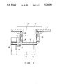
- FIG. 3 shows in a magnified fashion a driving mechanism of a base which supports the arm and the storing member included in the apparatus shown in FIG. 1;
- FIG. 4 is a perspective view showing in a magnified fashion the driving mechanism of the arm and the storing member included in the apparatus shown in FIG. 1;
- FIG. 5 is a cross sectional view showing in a magnified fashion the internal structure of the arm included in the apparatus shown in FIG. 1;
- FIGS. 6A and 6E sequentially show how the arm and the storing member shown in FIG. 1 are operated.
- FIG. 7 is a perspective view schematically showing a modification of the arm.
- FIG. 1 The accompanying drawings collectively show a vacuum processing apparatus according to an embodiment of the present invention.
- the apparatus of the embodiment shown in these drawings is adapted for use in an etching treatment or an ashing treatment applied to an LCD substrate.
- the vacuum processing apparatus of the present invention comprises a first load lock chamber (vacuum chamber) 1 and a second load lock chamber 2 located adjacent to the first load lock chamber 1.
- a plurality of, e.g., three, vacuum process chambers 3a, 3b and 3c are arranged in the vicinity of the first load lock chamber 1.
- a gate valve 4 is provided in each of the open communicating regions between the first load lock chamber 1 and the second load lock chamber 2, between the first load lock chamber 1 and the vacuum process chamber 3a, between the first load lock chamber 1 and the vacuum process chamber 3b, between the first load lock chamber 1 and the vacuum process chamber 3c, and between the second load lock chamber 2 and an external region.
- Each of these gate valves 4 is constructed to be capable of hermetically closing and opening the communicating region.
- a mount 11 for supporting an LCD substrate S is arranged within each of the process chambers 3a, 3b and 3c.
- Projectable pins 12 for supporting the substrate S are provided at four corner portions of the mount 11.
- a transfer member 6 is arranged outside (in the lower portion in FIG. 1) the second load lock chamber 2.
- the transfer member 6 is put under the air atmosphere.
- Vertically movable tables (not shown) for supporting cassettes each housing LCD substrates are arranged on both sides of the transfer member 6.
- FIG. 1 shows the state that cassettes 5a and 5b are disposed on these vertically movable tables, respectively.
- Substrates which are to be treated are housed in, for example, the cassette 5a, with substrates after treatment being housed in the cassette 5b.
- the transfer member 6 comprises arms 15a and 15b superposed one upon the other and a base 16 for rotatably supporting these arms. These arms 15a, 15b are integrally moved forward and backward by the base 16. Each of these arms 15a and 15b is provided with four projections 17 for supporting the substrate.
- the projection 17 is formed of an elastic material having a high friction coefficient such as a synthetic resin for preventing the substrate from slipping or sliding off.
- the two arms 15a and 15b of the transfer member 6 permit transferring two substrates at a time. To be more specific, two substrates are taken at a time out of, for example, the cassette 5a by the arms 15a and 15b of the transfer member 6. Likewise, two substrates after treatment are simultaneously put in the cassette 5b. The height of each of these cassettes 5a and 5b is adjusted by the vertically movable table to determine the positions at which the substrates are taken out of or put in these cassettes.
- a pair of racks 22 are arranged within the second load lock chamber 2 and respectively have two height levels corresponding to the vertical positions of the arms 15a, 15b of the transfer member 6. Naturally, two LCD substrates are simultaneously held within the second load lock chamber 2 by these racks 22.
- the racks 22 are movable in the vertical direction, and one of the two substrates held by these racks 22 is selectively taken out by a substrate transfer arm 7 which is described herein later.
- a pair of positioners 24 for aligning the substrate are arranged within the second load lock chamber 2. These positioners 24 are provided to face each other on an extension line of the diagonal of substrates disposed within the second load lock chamber 2.
- Each positioner 24 comprises a base 26 movable in a direction denoted by an arrow A and a pair of rollers 28a, 28b rotatably supported on the base 26. The two substrates held by the racks 22 are diagonally moved by the positioners 24 for the alignment. Further, optical sensors (not shown) for confirming the substrate alignment are disposed within the second load lock chamber 2.
- the substrate transfer arm 7 referred to previously is arranged within the first load lock chamber 1 together with a storing member 8 constructed to be capable of holding a plurality of LCD substrates. As shown in FIG. 2, these arm 7 and the storing member 8 are supported by a rotatable base 9.
- FIG. 3 schematically shows the driving system of the base 9.
- the base 9 is fixed to the upper end of a cylinder 34 extending through a floor 32 of the first load lock chamber 1. That portion of the cylinder 34 which is positioned below the floor 32 is covered with a cylindrical cover member 36 fixed to the floor 32.
- a seal 38 e.g., a magnetic fluid seal, and bearings 42 are arranged in the space between the cylinder 34 and the cover member 36.
- a motor 44 is fixed to the cover member 36 via a frame 43.
- a pulley 46 mounted to an output shaft of the motor 44 is connected to a pulley 48 arranged below the cylinder 34 via a timing belt 52. It follows that the cylinder 34 and the base 9 are driven by the motor 44.
- a motor 54 for driving the arm 7 and another motor 56 for vertically moving the storing member 8 are mounted to a lower portion of the cylinder 34. When the cylinder 34 is rotated, these motors 54 and 56 are rotated together with the cylinder 34.
- the output shaft of the motor 54 is connected to a pulley 58 arranged within the base 9.
- a timing belt 62 arranged within the base 9 is engaged with the pulley 58 and with another pulley 64 arranged at the tip portion of the base where the arm 7 is connected.
- the pulley 64 is fixed to the lower end portion of a shaft 66 acting as the rotating shaft of a first arm element 7a of the arm 7.
- the upper end portion of the shaft 66 is fixed to the first arm element 7a.
- a cylindrical cover 68 is disposed to cover the shaft 66.
- the lower end portion of the cover 68 is fixed to the base 9, and a pulley 72 is arranged at the upper end portion of the cover 68.
- bearings 74 are disposed within the space defined by the shaft 66, the base 9 and the cover 68.
- a timing belt 76 arranged within the first arm element 7a is engaged with the pulley 72 and with another pulley 78 arranged at the tip portion of the first arm element 7a where a second arm element 7b is connected to the first arm element.
- the pulley 78 is fixed to the lower end portion of a shaft 82 acting as a rotating shaft of the second arm element 7b.
- the upper end portion of the shaft 82 is fixed to the second arm element 7b.
- a cylindrical cover 84 is disposed to cover the shaft 82.
- the lower end portion of the cover 84 is fixed to the first arm element 7a, and the pulley 86 is mounted to the upper end portion of the cover 84.
- bearings 88 are disposed between the shaft 82 and the cover 84.
- a timing belt 92 arranged within the second arm element 7b is engaged with the pulley 86 and with another pulley 94 mounted at the tip portion of the second arm element 7b where a third arm element 7c is connected to the second arm element 7b.
- the pulley 94 is mounted at the lower end portion of a shaft 96 acting as a rotating shaft of the third arm element 7c.
- the upper end portion of the shaft 96 is fixed to the third arm element 7c.
- a cylindrical cover 98 is disposed to cover the shaft 96.
- the lower end portion of the cover 98 is fixed to the second arm element 7b.
- bearings 102 are disposed between the shaft 96 and the cover 98.
- the third arm element 7c is I-shaped as shown in FIG. 2.
- Four projections 104 for supporting the substrate S are mounted at end portions of the third arm element 7c.
- Each of these projections 104 is formed of an elastic material having a high frictional coefficient such as a synthetic rubber so as to prevent the substrate supported thereon from slipping or sliding off. An operation of the arm 7 will be described herein later.
- the output shaft of the motor 56 for driving the storing member 8 is joined to cylindrical hollow shaft 112 extending within the cylinder 34 in its axial direction.
- An internally threaded cylinder 114 is fixed to the upper portion of the hollow shaft 112.
- the internally threaded cylinder 114 is exposed to the outside from the base 9, and a shaft 116 having a ball screw formed therein is engaged with the exposed portion of the internally threaded cylinder 114
- the top portion of the shaft 116 is fixed to a bottom plate 142 of the storing member 8 by a screw 118.
- Linear guiding shafts 122 and 124 are fixed to the bottom plate 142 of the storing member 8 by screws 126 and 128. These shafts 122 and 124 extend through the central holes of guide cylinders 132 and 134, respectively, buried in the base 9 to reach the inner region of the cylinder 34. It follows that, if the internally threaded cylinder 114 is rotated by the motor 56, the linear guide shafts 122 and 124 act as a mechanism for stopping the rotation, with the result that the screw shaft 116 is moved up or down together with the storing member 8 and shafts 122 and 124 relative to the base 9.
- each of these supporting frames 144, 146 and 148 forms four stages of flat levels, with the result that four LCD substrates are housed at a time in these supporting frames.
- Supporting plates constituting each of the flat levels of these supporting frames are provided with projections 152 for supporting the substrate.
- Each of the projection 152 is formed of an elastic material having a high frictional coefficient such as a synthetic rubber so as to prevent the substrate supported thereon from slipping or sliding off.
- FIGS. 6A to 6E show how to use the arm 7 and the storing member 8. These drawings cover the case where the substrate S is moved by the arm 7 from the process chamber 3a to the process chamber 3c.
- the base 9 is rotated first to bring the arm 7 to a transferring position.
- the arm 7 is positioned in front of the process chamber 3a.
- the arm 7 is stretched to put the substrate S on the third arm element 7c.
- the substrate S put on the pins 12 of the mount 11 is transferred onto the arm 7 by the vertical movement of the pins 12.
- the arm 7 is gradually folded as shown in FIGS. 6B to 6D to transfer the substrate S to reach the storing member 8.
- the height of the storing member 8 is determined in advance to select one of the flat levels, on which the substrate S is to be disposed, of the storing member 8.
- the vertical position of the storing member 8 is determined such that the selected level of the storing member is positioned somewhat lower than the lower surface of the substrate S.
- the substrate S is transferred from the arm 7 onto the supporting plates of the selected level by an upward movements of the storing member 8.
- the base 9 is rotated to permit the arm 7 to be positioned in front of the process chamber 3c, as shown in FIG. 6E. If another substrate after treatment is left within the process chamber 3c in this stage, the treated or processed substrate is taken out of the process chamber 3c by the arm 7, as in the steps shown in FIGS. 6A to 6D. The substrate taken out of the process chamber 3c is transferred onto the supporting plates of another level by vertically moving the storing member 8. Then, the substrate carried from the process chamber 3a is put into the process chamber 3c and disposed on the mount 11.
- the mount 11 arranged in each of the process chambers 3a, 3b and 3c acts as a lower electrode.
- the mount 11 arranged in each of the process chambers 3a, 3b and 3c acts as a lower electrode.
- the substrate supporting position of the arm 7 in the step of putting the substrate on the storing member 8 is deviated from the substrate supporting position of the arm 7 in the step of receiving the substrate from the storing member 8. It is possible to control as desired the position of the substrate on the lower electrode by suitably adjusting the amount of deviation noted. Incidentally, this adjustment can be controlled by a software of a computer serving to control the movement of the arm 7.
- the air within the second load lock chamber 2 is discharged to set up a predetermined degree of vacuum within the second load lock chamber 2.
- the two substrates disposed on the racks 22 are aligned by the positioners 24.
- the gate 4 between the first load lock chamber 1 and the second load lock chamber 2 is opened, and the two substrates within the second load lock chamber 2 are successively transferred by the arm 7 into the storing member 8 positioned behind the arm 7.
- one of the substrates is transferred by the arm 7 from the first load lock chamber 1 into a predetermined one of the process chambers 3a, 3b and 3c for applying a predetermined treatment to the substrate.
- the substrate may be successively transferred into these process chambers 3a, 3b and 3c for applying different treatments such as an etching treatment and an ashing treatment to the substrate. It is also possible to apply the same treatment simultaneously to a plurality of substrates in these process chambers.
- the substrate after treatment is taken out of these process chambers, followed by supplying another substrate into these process chambers for the treatment thereof.
- the substrate to be treated is disposed in advance on a predetermined level of the storing member 8.
- the substrate after treatment is disposed on another level of the storing member 8.
- the substrate S is transferred into the second load lock chamber 2 by the arm 7. Then, the substrate S is transferred by the transfer member 6 from the second load lock chamber 2 to the outside so as to be housed in the cassette 5b.
- the vacuum processing apparatus of the present invention comprises the storing member 8, making it possible to put and take the LCD substrate S in and out of the process chamber in a short time substantially equal to that of the conventional apparatus comprising a plurality of arms 7.
- the particular construction of the present invention permits improving the through-put of the workpiece such as an LCD substrate.
- the particular construction of the present invention makes it possible to diminish the inner volumes of the first load lock chamber 1 and the first to third process chambers 3a to 3c, compared with the conventional apparatus comprising a plurality of arms 7. It is also possible to diminish the open area of the gate valve 4. It follows that the present invention permits suppressing the enlargement of the apparatus and suppressing the increase in the manufacturing cost.
- FIG. 7 shows a storing member 162, which is a modification of the storing member included in the apparatus described above.
- the storing member 162 is supported by a ceiling portion of the first load lock chamber 1 above an arm 164 which is substantially equal in its function to the substrate transfer arm 7.
- the storing member 162 is rotatable in synchronism with the rotation of the arm 164 and is movable in the vertical direction.
- the embodiment shown in FIG. 7 permits further miniaturizing the first load lock chamber 1, leading to a further cost saving.
- a single LCD substrate S alone can be supported by the storing member 162.
- the time required for putting and taking the substrate in and out of the process chamber is longer than in the embodiment described previously.
- the time in question is shorter than in the case where a storing member is not included in the apparatus, leading to a shortened operating time and, thus, to an improved through-put.
Abstract
Description
Claims (16)
Applications Claiming Priority (2)
| Application Number | Priority Date | Filing Date | Title |
|---|---|---|---|
| JP4-110506 | 1992-04-28 | ||
| JP4110506A JP3030160B2 (en) | 1992-04-28 | 1992-04-28 | Vacuum processing equipment |
Publications (1)
| Publication Number | Publication Date |
|---|---|
| US5306380A true US5306380A (en) | 1994-04-26 |
Family
ID=14537505
Family Applications (1)
| Application Number | Title | Priority Date | Filing Date |
|---|---|---|---|
| US08/053,389 Expired - Lifetime US5306380A (en) | 1992-04-28 | 1993-04-28 | Vacuum processing apparatus |
Country Status (3)
| Country | Link |
|---|---|
| US (1) | US5306380A (en) |
| JP (1) | JP3030160B2 (en) |
| KR (1) | KR0179385B1 (en) |
Cited By (29)
| Publication number | Priority date | Publication date | Assignee | Title |
|---|---|---|---|---|
| US5494494A (en) * | 1992-06-24 | 1996-02-27 | Anelva Corporation | Integrated module multi-chamber CVD processing system and its method for processing substrates |
| US5558482A (en) * | 1992-07-29 | 1996-09-24 | Tokyo Electron Limited | Multi-chamber system |
| US5588789A (en) * | 1995-07-06 | 1996-12-31 | Brooks Automation | Load arm for load lock |
| US5611655A (en) * | 1993-04-23 | 1997-03-18 | Tokyo Electron Limited | Vacuum process apparatus and vacuum processing method |
| US5636960A (en) * | 1992-07-29 | 1997-06-10 | Tokyo Electron Limited | Apparatus for detecting and aligning a substrate |
| US6120229A (en) * | 1999-02-01 | 2000-09-19 | Brooks Automation Inc. | Substrate carrier as batchloader |
| US6155768A (en) * | 1998-01-30 | 2000-12-05 | Kensington Laboratories, Inc. | Multiple link robot arm system implemented with offset end effectors to provide extended reach and enhanced throughput |
| US6491491B1 (en) * | 1997-10-30 | 2002-12-10 | Sankyo Seiki Mfg. Co., Ltd. | Articulated robot |
| US6503365B1 (en) * | 1998-04-21 | 2003-01-07 | Samsung Electronics Co., Ltd. | Multi-chamber system having compact installation set-up for an etching facility for semiconductor device manufacturing |
| US6519504B1 (en) * | 1995-07-19 | 2003-02-11 | Hitachi, Ltd. | Vacuum processing apparatus and semiconductor manufacturing line using the same |
| WO2003021645A2 (en) * | 2001-08-31 | 2003-03-13 | Asyst Technologies, Inc. | Wafer engine |
| US6630053B2 (en) * | 2000-08-22 | 2003-10-07 | Asm Japan K.K. | Semiconductor processing module and apparatus |
| US6709521B1 (en) * | 1999-09-06 | 2004-03-23 | Tokyo Electron Limited | Transfer apparatus and accommodating apparatus for semiconductor process, and semiconductor processing system |
| US20040095546A1 (en) * | 2002-11-16 | 2004-05-20 | Lee Sang Seok | Substrate bonding machine for liquid crystal display device |
| US20040123952A1 (en) * | 2002-12-05 | 2004-07-01 | Hur Gwang Ho | FPD fabricating apparatus |
| US20050083036A1 (en) * | 2003-03-18 | 2005-04-21 | Stefan Schneidewind | Apparatus for testing substrates |
| US20060000823A1 (en) * | 2003-11-19 | 2006-01-05 | Surgrx, Inc. | Polymer compositions exhibiting a PTC property and methods of fabrication |
| US20060163519A1 (en) * | 2004-12-22 | 2006-07-27 | Tokyo Electron Limited | Vacuum processing apparatus |
| US20060204356A1 (en) * | 2005-03-08 | 2006-09-14 | Asm Japan K.K. | Semiconductor-manufacturing apparatus equipped with cooling stage and semiconductor-manufacturing method using same |
| US7217076B2 (en) | 2001-08-31 | 2007-05-15 | Asyst Technologies, Inc. | Semiconductor material handling system |
| US7293950B2 (en) | 2001-08-31 | 2007-11-13 | Aysts Technologies, Inc. | Universal modular wafer transport system |
| US20080100852A1 (en) * | 2006-10-26 | 2008-05-01 | Tokyo Electron Limited | Detecting apparatus and detecting method |
| US20090263230A1 (en) * | 2008-04-18 | 2009-10-22 | Hwang Young Joo | Cluster apparatus for processing substrate and method for processing substrate using cluster apparatus |
| US20100295244A1 (en) * | 2007-04-04 | 2010-11-25 | Koninklijke Philips Electronics N.V. | Determining stress level based on the performance of the person in a game or puzzle |
| US20100314552A1 (en) * | 2009-06-11 | 2010-12-16 | Nissin Ion Equipment Co., Ltd. | Ion implanter |
| CN101158767B (en) * | 2002-11-16 | 2011-01-05 | 乐金显示有限公司 | Substrate bonding machine for liquid crystal display device |
| US20110182702A1 (en) * | 2008-10-07 | 2011-07-28 | Kawasaki Jukogyo Kabushiki Kaisha | Substrate transfer robot and substrate transfer system |
| US20130028691A1 (en) * | 2007-09-22 | 2013-01-31 | Dynamic Micro Systems, Semiconductor Equipment Gmbh | Transfer mechanism with multiple wafer handling capability |
| US9924263B2 (en) | 2013-03-13 | 2018-03-20 | Thx Ltd. | Slim profile loudspeaker |
Citations (4)
| Publication number | Priority date | Publication date | Assignee | Title |
|---|---|---|---|---|
| US4661196A (en) * | 1984-10-22 | 1987-04-28 | Texas Instruments Incorporated | Plasma etch movable substrate |
| US4715921A (en) * | 1986-10-24 | 1987-12-29 | General Signal Corporation | Quad processor |
| US5138973A (en) * | 1987-07-16 | 1992-08-18 | Texas Instruments Incorporated | Wafer processing apparatus having independently controllable energy sources |
| US5164034A (en) * | 1989-09-08 | 1992-11-17 | Tokyo Electron Limited | Apparatus and method for processing substrate |
-
1992
- 1992-04-28 JP JP4110506A patent/JP3030160B2/en not_active Expired - Fee Related
-
1993
- 1993-04-24 KR KR1019930006916A patent/KR0179385B1/en not_active IP Right Cessation
- 1993-04-28 US US08/053,389 patent/US5306380A/en not_active Expired - Lifetime
Patent Citations (4)
| Publication number | Priority date | Publication date | Assignee | Title |
|---|---|---|---|---|
| US4661196A (en) * | 1984-10-22 | 1987-04-28 | Texas Instruments Incorporated | Plasma etch movable substrate |
| US4715921A (en) * | 1986-10-24 | 1987-12-29 | General Signal Corporation | Quad processor |
| US5138973A (en) * | 1987-07-16 | 1992-08-18 | Texas Instruments Incorporated | Wafer processing apparatus having independently controllable energy sources |
| US5164034A (en) * | 1989-09-08 | 1992-11-17 | Tokyo Electron Limited | Apparatus and method for processing substrate |
Cited By (50)
| Publication number | Priority date | Publication date | Assignee | Title |
|---|---|---|---|---|
| US5505779A (en) * | 1992-06-24 | 1996-04-09 | Anelva Corporation | Integrated module multi-chamber CVD processing system and its method for processing substrates |
| US5494494A (en) * | 1992-06-24 | 1996-02-27 | Anelva Corporation | Integrated module multi-chamber CVD processing system and its method for processing substrates |
| US5558482A (en) * | 1992-07-29 | 1996-09-24 | Tokyo Electron Limited | Multi-chamber system |
| US5636960A (en) * | 1992-07-29 | 1997-06-10 | Tokyo Electron Limited | Apparatus for detecting and aligning a substrate |
| US5611655A (en) * | 1993-04-23 | 1997-03-18 | Tokyo Electron Limited | Vacuum process apparatus and vacuum processing method |
| US5588789A (en) * | 1995-07-06 | 1996-12-31 | Brooks Automation | Load arm for load lock |
| EP0836577A1 (en) * | 1995-07-06 | 1998-04-22 | Brooks Automation, Inc. | Load arm for load lock |
| EP0836577A4 (en) * | 1995-07-06 | 2006-07-19 | Brooks Automation Inc | Load arm for load lock |
| US6519504B1 (en) * | 1995-07-19 | 2003-02-11 | Hitachi, Ltd. | Vacuum processing apparatus and semiconductor manufacturing line using the same |
| US6491491B1 (en) * | 1997-10-30 | 2002-12-10 | Sankyo Seiki Mfg. Co., Ltd. | Articulated robot |
| US6155768A (en) * | 1998-01-30 | 2000-12-05 | Kensington Laboratories, Inc. | Multiple link robot arm system implemented with offset end effectors to provide extended reach and enhanced throughput |
| US6503365B1 (en) * | 1998-04-21 | 2003-01-07 | Samsung Electronics Co., Ltd. | Multi-chamber system having compact installation set-up for an etching facility for semiconductor device manufacturing |
| US7776226B2 (en) | 1998-04-21 | 2010-08-17 | Samsung Electronics Co., Ltd. | Multi-chamber system having compact installation set-up for an etching facility for semiconductor device manufacturing |
| US20030073323A1 (en) * | 1998-04-21 | 2003-04-17 | Kim Ki-Sang | Multi-chamber system having compact installation set-up for an etching facility for semiconductor device manufacturing |
| US6930050B2 (en) | 1998-04-21 | 2005-08-16 | Samsung Electronics Co., Ltd. | Multi-chamber system having compact installation set-up for an etching facility for semiconductor device manufacturing |
| US20050236092A1 (en) * | 1998-04-21 | 2005-10-27 | Kim Ki-Sang | Multi-chamber system having compact installation set-up for an etching facility for semiconductor device manufacturing |
| US6120229A (en) * | 1999-02-01 | 2000-09-19 | Brooks Automation Inc. | Substrate carrier as batchloader |
| US6709521B1 (en) * | 1999-09-06 | 2004-03-23 | Tokyo Electron Limited | Transfer apparatus and accommodating apparatus for semiconductor process, and semiconductor processing system |
| US6630053B2 (en) * | 2000-08-22 | 2003-10-07 | Asm Japan K.K. | Semiconductor processing module and apparatus |
| US7066707B1 (en) | 2001-08-31 | 2006-06-27 | Asyst Technologies, Inc. | Wafer engine |
| WO2003021645A3 (en) * | 2001-08-31 | 2003-07-24 | Asyst Technologies | Wafer engine |
| WO2003021645A2 (en) * | 2001-08-31 | 2003-03-13 | Asyst Technologies, Inc. | Wafer engine |
| US7217076B2 (en) | 2001-08-31 | 2007-05-15 | Asyst Technologies, Inc. | Semiconductor material handling system |
| US7293950B2 (en) | 2001-08-31 | 2007-11-13 | Aysts Technologies, Inc. | Universal modular wafer transport system |
| CN100385293C (en) * | 2002-11-16 | 2008-04-30 | Lg.菲利浦Lcd株式会社 | Substrate bonding machine for liquid crystal display device |
| US7886793B2 (en) | 2002-11-16 | 2011-02-15 | Lg Display Co., Ltd. | Substrate bonding machine for liquid crystal display device |
| US20040095546A1 (en) * | 2002-11-16 | 2004-05-20 | Lee Sang Seok | Substrate bonding machine for liquid crystal display device |
| CN101158767B (en) * | 2002-11-16 | 2011-01-05 | 乐金显示有限公司 | Substrate bonding machine for liquid crystal display device |
| US7275577B2 (en) * | 2002-11-16 | 2007-10-02 | Lg.Philips Lcd Co., Ltd. | Substrate bonding machine for liquid crystal display device |
| US20040123952A1 (en) * | 2002-12-05 | 2004-07-01 | Hur Gwang Ho | FPD fabricating apparatus |
| US20050083036A1 (en) * | 2003-03-18 | 2005-04-21 | Stefan Schneidewind | Apparatus for testing substrates |
| US7196507B2 (en) * | 2003-08-28 | 2007-03-27 | Suss Microtec Testsystems (Gmbh) | Apparatus for testing substrates |
| US20060000823A1 (en) * | 2003-11-19 | 2006-01-05 | Surgrx, Inc. | Polymer compositions exhibiting a PTC property and methods of fabrication |
| US20060163519A1 (en) * | 2004-12-22 | 2006-07-27 | Tokyo Electron Limited | Vacuum processing apparatus |
| US8113487B2 (en) | 2004-12-22 | 2012-02-14 | Tokyo Electron Limited | Vacuum processing apparatus |
| US8523138B2 (en) | 2004-12-22 | 2013-09-03 | Tokyo Electron Limited | Vacuum processing apparatus |
| US7611124B2 (en) * | 2004-12-22 | 2009-11-03 | Tokyo Electron Limited | Vacuum processing apparatus |
| US20060204356A1 (en) * | 2005-03-08 | 2006-09-14 | Asm Japan K.K. | Semiconductor-manufacturing apparatus equipped with cooling stage and semiconductor-manufacturing method using same |
| US7467916B2 (en) | 2005-03-08 | 2008-12-23 | Asm Japan K.K. | Semiconductor-manufacturing apparatus equipped with cooling stage and semiconductor-manufacturing method using same |
| US7470098B2 (en) * | 2006-10-26 | 2008-12-30 | Tokyo Electron Limited | Detecting apparatus and detecting method |
| US20080100852A1 (en) * | 2006-10-26 | 2008-05-01 | Tokyo Electron Limited | Detecting apparatus and detecting method |
| US20100295244A1 (en) * | 2007-04-04 | 2010-11-25 | Koninklijke Philips Electronics N.V. | Determining stress level based on the performance of the person in a game or puzzle |
| US20130028691A1 (en) * | 2007-09-22 | 2013-01-31 | Dynamic Micro Systems, Semiconductor Equipment Gmbh | Transfer mechanism with multiple wafer handling capability |
| US9728436B2 (en) * | 2007-09-22 | 2017-08-08 | Brooks Automation, Gmbh | Transfer mechanism with multiple wafer handling capability |
| US20090263230A1 (en) * | 2008-04-18 | 2009-10-22 | Hwang Young Joo | Cluster apparatus for processing substrate and method for processing substrate using cluster apparatus |
| US20110182702A1 (en) * | 2008-10-07 | 2011-07-28 | Kawasaki Jukogyo Kabushiki Kaisha | Substrate transfer robot and substrate transfer system |
| US8882431B2 (en) * | 2008-10-07 | 2014-11-11 | Kawasaki Jukogyo Kabushiki Kaisha | Substrate transfer robot and substrate transfer system |
| US20100314552A1 (en) * | 2009-06-11 | 2010-12-16 | Nissin Ion Equipment Co., Ltd. | Ion implanter |
| US8143595B2 (en) * | 2009-06-11 | 2012-03-27 | Nissin Ion Equipment Co., Ltd. | Ion implanter |
| US9924263B2 (en) | 2013-03-13 | 2018-03-20 | Thx Ltd. | Slim profile loudspeaker |
Also Published As
| Publication number | Publication date |
|---|---|
| JPH05304112A (en) | 1993-11-16 |
| KR930022122A (en) | 1993-11-23 |
| JP3030160B2 (en) | 2000-04-10 |
| KR0179385B1 (en) | 1999-05-01 |
Similar Documents
| Publication | Publication Date | Title |
|---|---|---|
| US5306380A (en) | Vacuum processing apparatus | |
| KR100636491B1 (en) | Substrate support | |
| JP4620453B2 (en) | Large board inspection system | |
| JP2622046B2 (en) | Substrate transfer device | |
| US5509771A (en) | Vacuum processing apparatus | |
| US5989346A (en) | Semiconductor processing apparatus | |
| US7919972B2 (en) | Integrated substrate transfer module | |
| US8157496B2 (en) | Substrate processing apparatus and substrate transfer method | |
| JP2001356353A (en) | Assembly device for substrate | |
| US5947675A (en) | Cassette transfer mechanism | |
| JP2000284295A (en) | Method and apparatus for assembling substrate | |
| US5944475A (en) | Rotated, orthogonal load compatible front-opening interface | |
| JPH10163293A (en) | Treating device | |
| US20060273815A1 (en) | Substrate support with integrated prober drive | |
| KR100514771B1 (en) | Method and apparatus for assembling substrate | |
| WO1999052143A1 (en) | Alignment processing mechanism and semiconductor processing device using it | |
| JP3350234B2 (en) | Object buffer device, processing device using the same, and method of transporting the same | |
| JP3172375B2 (en) | Substrate transfer device | |
| JP3260427B2 (en) | Vacuum processing apparatus and substrate transfer method in vacuum processing apparatus | |
| JPH05198659A (en) | Plasma processor | |
| JPH08297279A (en) | Device and method for transferring substrate | |
| JPH1131729A (en) | Substrate housing vessel supply device | |
| KR102617398B1 (en) | Substrate transport apparatus, substrate processing apparatus, and substrate transport method | |
| JP4043029B2 (en) | Substrate transport apparatus and substrate processing apparatus | |
| JP3242145B2 (en) | Substrate transfer device |
Legal Events
| Date | Code | Title | Description |
|---|---|---|---|
| STPP | Information on status: patent application and granting procedure in general |
Free format text: APPLICATION UNDERGOING PREEXAM PROCESSING |
|
| AS | Assignment |
Owner name: TOKYO ELECTRON YAMANASHI LIMITED, JAPAN Free format text: ASSIGNMENT OF ASSIGNORS INTEREST;ASSIGNOR:HIROKI, TUTOMU;REEL/FRAME:006842/0658 Effective date: 19930420 Owner name: TOKYO ELECTRON LIMITED, JAPAN Free format text: ASSIGNMENT OF ASSIGNORS INTEREST;ASSIGNOR:HIROKI, TUTOMU;REEL/FRAME:006842/0658 Effective date: 19930420 |
|
| FEPP | Fee payment procedure |
Free format text: PAYOR NUMBER ASSIGNED (ORIGINAL EVENT CODE: ASPN); ENTITY STATUS OF PATENT OWNER: LARGE ENTITY |
|
| AS | Assignment |
Owner name: TOKYO ELECTRON LIMITED, JAPAN Free format text: ASSIGNMENT OF ASSIGNORS INTEREST;ASSIGNOR:TOKYO ELECTRON YAMANASHI LIMITED;REEL/FRAME:008669/0516 Effective date: 19970221 |
|
| FPAY | Fee payment |
Year of fee payment: 4 |
|
| FEPP | Fee payment procedure |
Free format text: PAYER NUMBER DE-ASSIGNED (ORIGINAL EVENT CODE: RMPN); ENTITY STATUS OF PATENT OWNER: LARGE ENTITY Free format text: PAYOR NUMBER ASSIGNED (ORIGINAL EVENT CODE: ASPN); ENTITY STATUS OF PATENT OWNER: LARGE ENTITY |
|
| FPAY | Fee payment |
Year of fee payment: 8 |
|
| FPAY | Fee payment |
Year of fee payment: 12 |