US5307337A - Optical disk drive having a low-emission high-bandwidth laser driver - Google Patents
Optical disk drive having a low-emission high-bandwidth laser driver Download PDFInfo
- Publication number
- US5307337A US5307337A US07/915,422 US91542292A US5307337A US 5307337 A US5307337 A US 5307337A US 91542292 A US91542292 A US 91542292A US 5307337 A US5307337 A US 5307337A
- Authority
- US
- United States
- Prior art keywords
- laser
- transistor
- power level
- light
- modulating
- Prior art date
- Legal status (The legal status is an assumption and is not a legal conclusion. Google has not performed a legal analysis and makes no representation as to the accuracy of the status listed.)
- Expired - Fee Related
Links
Images


Classifications
-
- G—PHYSICS
- G11—INFORMATION STORAGE
- G11B—INFORMATION STORAGE BASED ON RELATIVE MOVEMENT BETWEEN RECORD CARRIER AND TRANSDUCER
- G11B7/00—Recording or reproducing by optical means, e.g. recording using a thermal beam of optical radiation by modifying optical properties or the physical structure, reproducing using an optical beam at lower power by sensing optical properties; Record carriers therefor
- G11B7/12—Heads, e.g. forming of the optical beam spot or modulation of the optical beam
- G11B7/125—Optical beam sources therefor, e.g. laser control circuitry specially adapted for optical storage devices; Modulators, e.g. means for controlling the size or intensity of optical spots or optical traces
- G11B7/126—Circuits, methods or arrangements for laser control or stabilisation
-
- G—PHYSICS
- G11—INFORMATION STORAGE
- G11B—INFORMATION STORAGE BASED ON RELATIVE MOVEMENT BETWEEN RECORD CARRIER AND TRANSDUCER
- G11B7/00—Recording or reproducing by optical means, e.g. recording using a thermal beam of optical radiation by modifying optical properties or the physical structure, reproducing using an optical beam at lower power by sensing optical properties; Record carriers therefor
- G11B7/12—Heads, e.g. forming of the optical beam spot or modulation of the optical beam
- G11B7/125—Optical beam sources therefor, e.g. laser control circuitry specially adapted for optical storage devices; Modulators, e.g. means for controlling the size or intensity of optical spots or optical traces
Definitions
- the present invention pertains to the field of optical recording systems. More particularly, the present invention relates to implementing a low emission driver having a high bandwidth for driving a laser used to read and write data from/to an optical storage medium.
- optical-based data storage systems are commercially competitive due to their high storage density, relatively low cost, and random access capability.
- magneto-optical data storage systems offer the added flexibility of allowing an optical medium to be erased and new data written in place of the erased section. This feature grants a user the capability to reuse an optical medium many times over by erasing old data and substituting new data in place thereof.
- magneto-optical recording operates in the following manner.
- Data is stored as a series of binary bits (i.e., 1s and 0s).
- a laser beam is focused onto an optical medium, usually by means of a lens assembly. Initially, the optical medium is perpendicularly magnetized. To write a "1," the laser beam is pulsed at a high power for a short duration. This raises the temperature of the optical medium to such a degree that an externally applied magnetic field reverses the direction of magnetization in the heated region. When the medium returns to its lower ambient temperature, the "domain" retains its reverse magnetization.
- the domains are "erased” by using the laser to perform the same thermal process used to write the data, except that an oppositely directed external magnetic field is applied. Thereby, the domains revert back to their original magnetization.
- the stored data is read from the optical medium based on the polar curve principle.
- This principle states that linearly polarized light, reflected from a perpendicularly magnetized medium, is rotated according to the direction of magnetization.
- the magnetization transitions of the domains stored on the media can be read by determining the direction of the plane of polarization of the reflected light.
- the same laser used to write the data is also used to generate the reflected light for reading the stored data, except that its power is reduced to avoid inadvertently writing data onto the medium.
- This type of recording system has one common problem in that, typically, there is no isolation between the laser and the storage medium. Consequently, the light generated by the laser used to read the data stored on the medium is reflected from the medium and directed back at the laser. As a result of this feedback light, the laser becomes unstable. The instability interferes with the reading of data from the medium. That is to say, the instability is a form of noise.
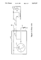
- FIG. 1 illustrates a typical prior art RF modulator and laser driver used in magneto-optical recording systems.
- a laser driver 100 is used to drive a laser diode 101.
- the RF modulator 102 is implemented to modulate the laser diode 101 at relatively high frequencies (approximately 300-600 MHz). By modulating the laser diode 101, instabilities due to reflected light from the medium are minimized.
- RF energy is hard to contain and channel because it tends to radiate to the surroundings and to transmit through wiring.
- the modulator is enclosed within an electro-magnetic interference (EMI) shielding box 103.
- Inductor 104, feed-through capacitor 105, and resistor 106 are implemented as a low-pass filter to reduce the amount of RF energy being transmitted back to laser driver 100 through line 107. If the LRC 104-106 low-pass filter were not implemented, the RF energy from modulator 102 would trace back to laser driver 100 through line 107, thereby creating a D.C. offset in pre-amplifier 108.
- the D.C. offset can be compensated, but since RF pickup varies from one device to another, each device must be individually compensated manually. Such a process is labor intensive, costly, and time-consuming.
- an LRC 104-106 low-pass filter is disadvantageous because it limits the bandwidth of laser driver 100 in WRITE mode operations.
- the same low-pass filter which reduces the RF energy from tracing back to the laser driver during READ operations also acts to inhibit the bandwidth of the laser driver during WRITE operations.
- PWM pulse width modulation
- One prior art method of implementing a high bandwidth WRITE mode is to output a relatively strong signal from the laser driver to drive the laser diode.
- this method is disadvantageous because the strong signal on the wire 107 leading from the laser driver 100 to the EMI shielding 103 causes serious radiated emission problems.
- the problem is worsened by the fact that the output from the laser driver contains a high level of harmonics due to the fast rise and fall times of the write pulses.
- the emission problems are so serious as to cause the magneto-optical data storage system to fail Class "A" EMI standards set forth by the Federal Communication Commission (FCC).
- FCC Federal Communication Commission
- one object of the present invention is to provide precise control of the laser power when writing data to a storage medium.
- Another object of the present invention is to reduce the amount of RF energy being transmitted to the driver pre-amplifier, so that any induced D.C. offset is minimized.
- Another object of the present invention is to minimize the radiated emissions from the output of the laser driver.
- Another object of the present invention is to maximize the bandwidth of the laser power control loop.
- Another object of the present invention is to incorporate the RF modulator and the output stage of the laser driver on a hybrid circuit and to enclose the hybrid circuit in EMI shielding.
- an optical recording system having an RF modulator which modulates the laser during READ mode, in order to improve the stability of the laser.
- the output stage of the laser driver is placed in close physical proximity to the laser.
- the RF modulator and the output stage of the laser driver are implemented on a hybrid circuit.
- the hybrid circuit, along with the laser, are enclosed within EMI shielding to contain the RF energy emitted from the RF modulator.
- the transistor of the laser driver's output stage inhibits the RF energy from being transmitted back to the rest of the laser driver circuitry.
- a low-level signal is sufficient to drive the base of the transistor. Thereby, the radiation from this signal is, correspondingly, of a low level.
- WRITE mode the power of the light beam output from the laser is measured. This information is fed back as an input to control the laser power.
- a high bandwidth (>50 MHz) laser power control loop is implemented. Since the transistor effectively blocks the RF energy, a low-pass filter is not necessary. Hence, a high bandwidth control loop can be implemented in the present invention.
- FIG. 1 illustrates a typical prior art RF modulator and laser driver in a magneto-optical recording system.
- FIG. 2 illustrates a magneto-optical recording system as may be utilized by the currently preferred embodiment of the present invention.
- FIG. 3 illustrates the lens assembly and the laser power control loop of the currently preferred embodiment of the present invention.
- FIG. 4 illustrates the laser driver, RF modulator, and laser diode of the currently preferred embodiment of the present invention.
- FIG. 5 is a circuit diagram illustrating the output stage of the laser driver and the RF modulator comprising an oscillator and an amplifier/modulator.
- FIG. 2 illustrates a magneto-optical disk drive system 200 as may be utilized by the preferred embodiment of the present invention.
- the magneto-optical disk drive system 200 is comprised of a SCSI interface 201 which provides an interface between the disk drive system 200 and external instrumentation, usually a computer.
- the interface 201 is coupled to a controller microprocessor 202 and to memory 203.
- Controller microprocessor 202 communicates with microprocessor 204 and instructs it per a program stored in memory 203.
- Controller microprocessor 202 is also coupled to disk controller hardware 205.
- Disk controller hardware 205 receives data signals read from the disk 210 via read/write channel 208 and converts it into a byte format. Likewise, when data is written via read/write channel 208, disk controller hardware 205 converts the data into a format compatible for storing on disk 210.
- Microprocessor 204 controls the spindle motor 206, servo mechanism 207, read/write channel 208, laser power controller 209, and laser driver 215.
- Spindle motor 206 spins disk 210
- servo mechanism 207 controls the movement of the lens assembly 212 to access each of the tracks of data on disk 210.
- Read/write channel 208 passes the signals read from and written to disk 210.
- Laser power controller 209 controls laser driver 213 which sets the power of the laser beam used to read and write the data.
- the light reflected from disk 210 is detected and fed back through loop 214 to microprocessor 204. Thereby, microprocessor 204 can effectively control the laser pulse.
- RF modulator 102 is implemented to provide laser stability by modulating the laser.
- FIG. 3 illustrates the laser driver 215, RF modulator 102, laser diode 301, lens assembly, and feedback loop in greater detail.
- the microprocessor commands that a signal be generated and sent to laser driver 215 for driving laser diode 301 at a READ power level of approximately 1.5 mW.
- Laser diode 301 emits light which is collimated by lens 302.
- the collimated light beam passes through beam splitters 303 and 304.
- the incident beam out of beam splitters 303 and 304 is deflected off mirror 305 and passed through lens 306.
- Lens 306 is a read/write head used to focus the incident beam onto optical disk 307.
- a tracking motor coil (not shown) controls the movement of mirror 305 and lens 306 so that the focused light beam can access radial locations across optical disk 307.
- the written domains which are arranged in tracks on optical disk 307, modulate and reflect the light beam back through lens 306.
- This modulated light beam is deflected by mirror 305 back through beam splitter 304 which splits the beam. Part of the beam is directed to lens 308 which focuses the beam onto pin-diode detectors 309. Detectors 309 produce an electrical signal which is dependent on the modulation of the reflected light beam.
- This electrical signal is routed to the microprocessor so that data stored on optical disk 307 can be passed as digital bits to a computer system.
- the other part of the reflected beam passes through beam splitter 303 and is directed back at laser diode 301.
- laser diode 301 is modulated by RF modulator 102.
- the frequency of RF modulator 102 is approximately 1 GHz.
- the microprocessor commands a signal be generated and sent to laser driver 100 for driving laser diode 301 at a WRITE power level of approximately 7.5 mW.
- Laser diode 501 emits light which is collimated by lens 302.
- the collimated light is passed through beam splitters 303 and 304 and reflected off mirror 305 onto lens 306.
- Lens 306 focuses the collimated light onto optical disk 307.
- the focused light heats up a particular domain, thereby "writing" data onto the optical disk.
- the light used to write data is also reflected from optical disk through lens 306 to mirror 305.
- the reflected light is directed back through beam splitters 304 and 303.
- Beam splitter 303 splits the reflected light so that a portion of the light passes through lens 310.
- Lens 310 focuses the reflected light onto power monitor detector diode 311.
- Detector diode 311 outputs an electrical signal which is proportional to the power of the reflected light. Based on this signal, the microprocessor adjusts the level by which the laser diode is driven. In short, the output power of the laser is measured and compared with the desired WRITE power level. Any noted differences are fed back as an input to adjust the laser's WRITE power level. Consequently, a faster laser power control loop (i.e., a higher bandwidth) results in tighter control over the WRITE pulse, which translates to a more precisely written domain. In the currently preferred embodiment of the present invention, the bandwidth of the laser power control loop is over 50 MHz.
- FIG. 4 is a block diagram illustrating the laser driver 215, RF modulator 102, and laser diode 301 of the currently preferred embodiment of the present invention.
- the output stage, namely transistor 401, of the laser driver has been moved so that it is in close physical proximity to the laser diode 301.
- transistor 401 resides inside the EMI shielding box 103.
- EMI shielding box 103 is comprised of a solid metal box having good conductive properties; this box is grounded.
- pre-amplifier 108 can drive the base of transistor 401 using a relatively low-level signal.
- approximately 100-150 mA current is used to drive laser diode 301.
- beta value of 40 for transistor 401 only 2.5-3.75 mA is required at the base of transistor 401.
- This low-level signal results in a correspondingly low level of emissions on line 402.
- the emitter of transistor 401 is coupled to a +10 volt power supply, which is used to bias transistor 401.
- the amplified output from the collector of transistor 401 is sent through resistor 403 and inductor 404 to drive the anode of laser diode 301.
- RF modulator 102 is A.C. coupled through capacitor 405 to laser diode 301.
- the RF modulator 102 is powered by Vcc (+5 volts).
- the cumulative effects of feed-through capacitor 406, capacitor 408, inductor 404, and resistors 403 and 407 is to decrease the RF energy transmitted through line 402.
- the collector-to-base separation provided by transistor 401 significantly decreases the amount of RF energy transmitted through line 402 back to pre-amplifier 108.
- Resistor 403 is also utilized to reduce the current supplied to laser diode 301.
- Laser diode 301 is mounted inside the EMI shielding box 103. Consequently, the connection of ground lines is, likewise, inside shielding box 103 which minimizes radiation from the laser ground pin.
- a glass covered opening is provided in shielding box 103 to pass the emitted light to the lens assembly.
- FIG. 5 is a circuit diagram illustrating the components and their respective values comprising the laser driver output stage 501, the laser diode 301, and the RF modulator.
- the RF modulator is comprised of a 1.0 GHz oscillator 503 and a MMIC amplifier/modulator 504.
- Oscillator 503 operates off an 8 mA D.C. current supplied from the RF modulator control line 505.
- the output of oscillator 503 is A.C. coupled through a 3.3 pF capacitor 506 to the input of MMIC amplifier/modulator 504 which outputs a 1 GHz modulated RF to laser diode 301.
- the RF modulator and laser driver output stage are implemented as a hybrid circuit.
- Transistor 507 implemented in oscillator 503 is a 2N2857 die.
- the amplifier/modulator 504 is comprised of an IC part number UPC1678P.
- the hybrid circuit is mounted inside the EMI shielding box. Three lines are coupled to the hybrid circuit: a +5 volt line for toggling power on/off to the RF modulator, a control line driving the base of transistor 401 for controlling the power level of laser diode 301, and a +10 volt line supplying power to the emitter of transistor 401.
- an optical recording system having a low-emission high-bandwidth laser driver is disclosed.
Landscapes
- Physics & Mathematics (AREA)
- Optics & Photonics (AREA)
- Optical Head (AREA)
Abstract
Description
Claims (14)
Priority Applications (1)
| Application Number | Priority Date | Filing Date | Title |
|---|---|---|---|
| US07/915,422 US5307337A (en) | 1992-07-17 | 1992-07-17 | Optical disk drive having a low-emission high-bandwidth laser driver |
Applications Claiming Priority (1)
| Application Number | Priority Date | Filing Date | Title |
|---|---|---|---|
| US07/915,422 US5307337A (en) | 1992-07-17 | 1992-07-17 | Optical disk drive having a low-emission high-bandwidth laser driver |
Publications (1)
| Publication Number | Publication Date |
|---|---|
| US5307337A true US5307337A (en) | 1994-04-26 |
Family
ID=25435702
Family Applications (1)
| Application Number | Title | Priority Date | Filing Date |
|---|---|---|---|
| US07/915,422 Expired - Fee Related US5307337A (en) | 1992-07-17 | 1992-07-17 | Optical disk drive having a low-emission high-bandwidth laser driver |
Country Status (1)
| Country | Link |
|---|---|
| US (1) | US5307337A (en) |
Cited By (5)
| Publication number | Priority date | Publication date | Assignee | Title |
|---|---|---|---|---|
| US5495464A (en) * | 1993-01-20 | 1996-02-27 | Olympus Optical Co., Ltd. | Optical data recording/reproducing apparatus |
| US20040030230A1 (en) * | 2002-08-08 | 2004-02-12 | Norris Mark A. | Ferrite stabilized led drive |
| US20050053109A1 (en) * | 2002-06-03 | 2005-03-10 | Josh Hogan | Integrated multiple wavelength system |
| US6891868B2 (en) | 2001-05-08 | 2005-05-10 | Plasmon Lms, Inc. | Laser driver with noise reduction feedback for optical storage applications |
| US20180210151A1 (en) * | 2017-01-23 | 2018-07-26 | Ii-Vi Incorporated | Free Space Variable Optical Attenuator With Integrated Input/Output Power Monitors |
Citations (9)
| Publication number | Priority date | Publication date | Assignee | Title |
|---|---|---|---|---|
| US3798548A (en) * | 1971-09-08 | 1974-03-19 | Ameco Inc | Discrete cable television distribution system |
| US4238679A (en) * | 1978-12-07 | 1980-12-09 | Conrac Corporation | Dual-chamber ionization smoke detector assembly |
| US4635265A (en) * | 1984-06-13 | 1987-01-06 | Edward Weck & Company, Inc. | Power switching circuit for a pulsed laser |
| US4675872A (en) * | 1985-09-30 | 1987-06-23 | Harris Corporation | Driver unit for a laser Q-switch |
| US4817102A (en) * | 1988-04-18 | 1989-03-28 | Maurer Larry D | Acousto-electromagnetic hologistic resonant system |
| US4924470A (en) * | 1989-07-25 | 1990-05-08 | Gordon Ries | Laser diode control apparatus |
| US4924473A (en) * | 1989-03-28 | 1990-05-08 | Raynet Corporation | Laser diode protection circuit |
| US4974229A (en) * | 1986-12-22 | 1990-11-27 | Fanuc Ltd. | High-frequency discharge-exciting laser device |
| US5036519A (en) * | 1988-12-05 | 1991-07-30 | Ricoh Company, Ltd. | Semiconductor laser controller |
-
1992
- 1992-07-17 US US07/915,422 patent/US5307337A/en not_active Expired - Fee Related
Patent Citations (9)
| Publication number | Priority date | Publication date | Assignee | Title |
|---|---|---|---|---|
| US3798548A (en) * | 1971-09-08 | 1974-03-19 | Ameco Inc | Discrete cable television distribution system |
| US4238679A (en) * | 1978-12-07 | 1980-12-09 | Conrac Corporation | Dual-chamber ionization smoke detector assembly |
| US4635265A (en) * | 1984-06-13 | 1987-01-06 | Edward Weck & Company, Inc. | Power switching circuit for a pulsed laser |
| US4675872A (en) * | 1985-09-30 | 1987-06-23 | Harris Corporation | Driver unit for a laser Q-switch |
| US4974229A (en) * | 1986-12-22 | 1990-11-27 | Fanuc Ltd. | High-frequency discharge-exciting laser device |
| US4817102A (en) * | 1988-04-18 | 1989-03-28 | Maurer Larry D | Acousto-electromagnetic hologistic resonant system |
| US5036519A (en) * | 1988-12-05 | 1991-07-30 | Ricoh Company, Ltd. | Semiconductor laser controller |
| US4924473A (en) * | 1989-03-28 | 1990-05-08 | Raynet Corporation | Laser diode protection circuit |
| US4924470A (en) * | 1989-07-25 | 1990-05-08 | Gordon Ries | Laser diode control apparatus |
Cited By (7)
| Publication number | Priority date | Publication date | Assignee | Title |
|---|---|---|---|---|
| US5495464A (en) * | 1993-01-20 | 1996-02-27 | Olympus Optical Co., Ltd. | Optical data recording/reproducing apparatus |
| US6891868B2 (en) | 2001-05-08 | 2005-05-10 | Plasmon Lms, Inc. | Laser driver with noise reduction feedback for optical storage applications |
| US20050053109A1 (en) * | 2002-06-03 | 2005-03-10 | Josh Hogan | Integrated multiple wavelength system |
| US20040030230A1 (en) * | 2002-08-08 | 2004-02-12 | Norris Mark A. | Ferrite stabilized led drive |
| US6707257B2 (en) * | 2002-08-08 | 2004-03-16 | Datex-Ohmeda, Inc. | Ferrite stabilized LED drive |
| US20180210151A1 (en) * | 2017-01-23 | 2018-07-26 | Ii-Vi Incorporated | Free Space Variable Optical Attenuator With Integrated Input/Output Power Monitors |
| US10481332B2 (en) * | 2017-01-23 | 2019-11-19 | Ii-Vi Delaware, Inc. | Free space variable optical attenuator with integrated input/output power monitors |
Similar Documents
| Publication | Publication Date | Title |
|---|---|---|
| KR940011268B1 (en) | Stabilized-feedback control device for semiconductor | |
| EP0256827B1 (en) | Apparatus for recording and reproducing data into/from an optical disc | |
| US4701609A (en) | Semiconductor laser drive circuit with peak detection and control | |
| US5640381A (en) | Laser power-drive circuit having a scaling DAC supplying a scaled reference signal to a plurality of scaled DAC's that supply a plurality of scaled output signals | |
| US4819242A (en) | Semiconductor laser driver circuit | |
| US4787078A (en) | Optical data recording and reproducing system with control of high frequency superposed signal applied to semiconductor laser | |
| US5477557A (en) | Laser drive circuit with independently adjustable maximum and minimum power levels | |
| EP0405952B1 (en) | Semiconductor laser driving circuit | |
| US5495456A (en) | Magneto-optical recording and reproducing apparatus having a laser driving circuit which superimposes a signal having a frequency at least double the maximum recording signal frequency | |
| US5307337A (en) | Optical disk drive having a low-emission high-bandwidth laser driver | |
| US5574707A (en) | Pulse width control apparatus for optical disk | |
| US20060007805A1 (en) | Information storage apparatus | |
| US6301199B1 (en) | Magneto-optical recording medium and recording/reproducing apparatus therefor in which recorded magnetic domains are transferred from the recording layer to the reproducing layer | |
| JPH0963093A (en) | Laser light output control circuit | |
| US6930968B2 (en) | Semiconductor laser driving apparatus with filter to attenuate enhanced frequency component and optical disk apparatus including the same | |
| JP2887276B2 (en) | Laser diode power control device | |
| JP3359051B2 (en) | Magneto-optical recording / reproducing device | |
| JPH0737265A (en) | Optical information recorder | |
| US5771220A (en) | Output control apparatus of semiconductor laser device | |
| KR100208784B1 (en) | Laser power control circuit and method thereof in optical recording ang reproducing apparatus | |
| JPH05136501A (en) | Semiconductor laser drive circuit | |
| JPH0883948A (en) | Semiconductor laser device, information recording/ reproduction device and image recorder | |
| JPS61192043A (en) | Semiconductor laser driving device | |
| JP3440497B2 (en) | Laser diode drive circuit | |
| JPH09115167A (en) | Laser beam output control circuit |
Legal Events
| Date | Code | Title | Description |
|---|---|---|---|
| AS | Assignment |
Owner name: MAXOPTIX CORPORATION A CORP. OF DELAWARE, CALIF Free format text: ASSIGNMENT OF ASSIGNORS INTEREST.;ASSIGNOR:WOLOSZCZUK, EUGENIUSZ A.;REEL/FRAME:006227/0264 Effective date: 19920709 |
|
| FEPP | Fee payment procedure |
Free format text: PAYOR NUMBER ASSIGNED (ORIGINAL EVENT CODE: ASPN); ENTITY STATUS OF PATENT OWNER: LARGE ENTITY |
|
| FPAY | Fee payment |
Year of fee payment: 4 |
|
| AS | Assignment |
Owner name: TRANSAMERICA BUSINESS CREDIT CORPORATION, ILLINOIS Free format text: SECURITY AGREEMENT;ASSIGNOR:MAXOPTIX CORPORATION;REEL/FRAME:008842/0722 Effective date: 19971111 |
|
| AS | Assignment |
Owner name: COAST BUSINESS CREDIT, A DIVISION OF SOUTHERN PACI Free format text: SECURITY AGREEMENT;ASSIGNOR:MAXOPTIX CORPORATION;REEL/FRAME:009737/0179 Effective date: 19980918 |
|
| AS | Assignment |
Owner name: MAXOPITX CORPORATION, CALIFORNIA Free format text: RELEASE AND REASSIGNMENT;ASSIGNOR:TRANSAMERICA BUSINESS CREDIT CORPORATION;REEL/FRAME:009790/0313 Effective date: 19990222 |
|
| FPAY | Fee payment |
Year of fee payment: 8 |
|
| REMI | Maintenance fee reminder mailed | ||
| LAPS | Lapse for failure to pay maintenance fees | ||
| STCH | Information on status: patent discontinuation |
Free format text: PATENT EXPIRED DUE TO NONPAYMENT OF MAINTENANCE FEES UNDER 37 CFR 1.362 |
|
| FP | Lapsed due to failure to pay maintenance fee |
Effective date: 20060426 |