US5313421A - EEPROM with split gate source side injection - Google Patents
EEPROM with split gate source side injection Download PDFInfo
- Publication number
- US5313421A US5313421A US07/820,364 US82036492A US5313421A US 5313421 A US5313421 A US 5313421A US 82036492 A US82036492 A US 82036492A US 5313421 A US5313421 A US 5313421A
- Authority
- US
- United States
- Prior art keywords
- conductivity type
- channel region
- region
- control gate
- memory
- Prior art date
- Legal status (The legal status is an assumption and is not a legal conclusion. Google has not performed a legal analysis and makes no representation as to the accuracy of the status listed.)
- Expired - Lifetime
Links
- 238000002347 injection Methods 0.000 title abstract description 20
- 239000007924 injection Substances 0.000 title abstract description 20
- 230000015654 memory Effects 0.000 claims abstract description 97
- 238000012795 verification Methods 0.000 claims abstract description 7
- 229910021420 polycrystalline silicon Inorganic materials 0.000 claims description 50
- 238000009792 diffusion process Methods 0.000 claims description 23
- 230000005641 tunneling Effects 0.000 claims description 16
- 239000002019 doping agent Substances 0.000 claims description 9
- ZOXJGFHDIHLPTG-UHFFFAOYSA-N Boron Chemical compound [B] ZOXJGFHDIHLPTG-UHFFFAOYSA-N 0.000 claims description 5
- 229910052796 boron Inorganic materials 0.000 claims description 5
- 229910052751 metal Inorganic materials 0.000 claims description 3
- 239000002184 metal Substances 0.000 claims description 3
- SDTHIDMOBRXVOQ-UHFFFAOYSA-N 5-[bis(2-chloroethyl)amino]-6-methyl-1h-pyrimidine-2,4-dione Chemical compound CC=1NC(=O)NC(=O)C=1N(CCCl)CCCl SDTHIDMOBRXVOQ-UHFFFAOYSA-N 0.000 claims 1
- 238000012544 monitoring process Methods 0.000 claims 1
- 238000000034 method Methods 0.000 abstract description 17
- 238000003491 array Methods 0.000 abstract description 4
- 239000000758 substrate Substances 0.000 description 13
- 238000002955 isolation Methods 0.000 description 11
- 230000008569 process Effects 0.000 description 11
- 230000008901 benefit Effects 0.000 description 9
- 150000004767 nitrides Chemical class 0.000 description 8
- 230000015572 biosynthetic process Effects 0.000 description 7
- 230000008878 coupling Effects 0.000 description 7
- 238000010168 coupling process Methods 0.000 description 7
- 238000005859 coupling reaction Methods 0.000 description 7
- 238000010586 diagram Methods 0.000 description 6
- 230000006870 function Effects 0.000 description 6
- 239000007943 implant Substances 0.000 description 5
- VYPSYNLAJGMNEJ-UHFFFAOYSA-N Silicium dioxide Chemical compound O=[Si]=O VYPSYNLAJGMNEJ-UHFFFAOYSA-N 0.000 description 4
- XUIMIQQOPSSXEZ-UHFFFAOYSA-N Silicon Chemical group [Si] XUIMIQQOPSSXEZ-UHFFFAOYSA-N 0.000 description 4
- 238000013459 approach Methods 0.000 description 4
- PWPJGUXAGUPAHP-UHFFFAOYSA-N lufenuron Chemical compound C1=C(Cl)C(OC(F)(F)C(C(F)(F)F)F)=CC(Cl)=C1NC(=O)NC(=O)C1=C(F)C=CC=C1F PWPJGUXAGUPAHP-UHFFFAOYSA-N 0.000 description 4
- 229910052785 arsenic Inorganic materials 0.000 description 3
- RQNWIZPPADIBDY-UHFFFAOYSA-N arsenic atom Chemical compound [As] RQNWIZPPADIBDY-UHFFFAOYSA-N 0.000 description 3
- 230000005684 electric field Effects 0.000 description 3
- 238000005530 etching Methods 0.000 description 3
- 238000000059 patterning Methods 0.000 description 3
- 229910052710 silicon Inorganic materials 0.000 description 3
- 239000010703 silicon Substances 0.000 description 3
- 125000006850 spacer group Chemical group 0.000 description 3
- 229910052581 Si3N4 Inorganic materials 0.000 description 2
- 229910052681 coesite Inorganic materials 0.000 description 2
- 229910052906 cristobalite Inorganic materials 0.000 description 2
- 238000000151 deposition Methods 0.000 description 2
- 238000009826 distribution Methods 0.000 description 2
- 239000002784 hot electron Substances 0.000 description 2
- 238000004519 manufacturing process Methods 0.000 description 2
- 230000008520 organization Effects 0.000 description 2
- 230000003647 oxidation Effects 0.000 description 2
- 238000007254 oxidation reaction Methods 0.000 description 2
- 229920002120 photoresistant polymer Polymers 0.000 description 2
- 239000004065 semiconductor Substances 0.000 description 2
- 230000035945 sensitivity Effects 0.000 description 2
- 239000000377 silicon dioxide Substances 0.000 description 2
- HQVNEWCFYHHQES-UHFFFAOYSA-N silicon nitride Chemical compound N12[Si]34N5[Si]62N3[Si]51N64 HQVNEWCFYHHQES-UHFFFAOYSA-N 0.000 description 2
- 229910052682 stishovite Inorganic materials 0.000 description 2
- 238000012360 testing method Methods 0.000 description 2
- 229910052905 tridymite Inorganic materials 0.000 description 2
- 230000005689 Fowler Nordheim tunneling Effects 0.000 description 1
- 239000008186 active pharmaceutical agent Substances 0.000 description 1
- 230000004888 barrier function Effects 0.000 description 1
- 230000000295 complement effect Effects 0.000 description 1
- 239000002131 composite material Substances 0.000 description 1
- 239000004020 conductor Substances 0.000 description 1
- 238000005520 cutting process Methods 0.000 description 1
- 230000000593 degrading effect Effects 0.000 description 1
- 230000008021 deposition Effects 0.000 description 1
- 230000000694 effects Effects 0.000 description 1
- 230000008030 elimination Effects 0.000 description 1
- 238000003379 elimination reaction Methods 0.000 description 1
- 230000005669 field effect Effects 0.000 description 1
- 230000036039 immunity Effects 0.000 description 1
- 239000011810 insulating material Substances 0.000 description 1
- 238000005468 ion implantation Methods 0.000 description 1
- 238000005259 measurement Methods 0.000 description 1
- 230000007246 mechanism Effects 0.000 description 1
- 238000012986 modification Methods 0.000 description 1
- 230000004048 modification Effects 0.000 description 1
- 238000011017 operating method Methods 0.000 description 1
- 229920005591 polysilicon Polymers 0.000 description 1
- 238000002360 preparation method Methods 0.000 description 1
- 238000012545 processing Methods 0.000 description 1
- 230000005855 radiation Effects 0.000 description 1
- 230000001105 regulatory effect Effects 0.000 description 1
- 230000003252 repetitive effect Effects 0.000 description 1
- 229910021332 silicide Inorganic materials 0.000 description 1
- FVBUAEGBCNSCDD-UHFFFAOYSA-N silicide(4-) Chemical compound [Si-4] FVBUAEGBCNSCDD-UHFFFAOYSA-N 0.000 description 1
- 238000012546 transfer Methods 0.000 description 1
- 230000007704 transition Effects 0.000 description 1
Images


Classifications
-
- G—PHYSICS
- G11—INFORMATION STORAGE
- G11C—STATIC STORES
- G11C11/00—Digital stores characterised by the use of particular electric or magnetic storage elements; Storage elements therefor
- G11C11/56—Digital stores characterised by the use of particular electric or magnetic storage elements; Storage elements therefor using storage elements with more than two stable states represented by steps, e.g. of voltage, current, phase, frequency
- G11C11/5621—Digital stores characterised by the use of particular electric or magnetic storage elements; Storage elements therefor using storage elements with more than two stable states represented by steps, e.g. of voltage, current, phase, frequency using charge storage in a floating gate
- G11C11/5628—Programming or writing circuits; Data input circuits
- G11C11/5635—Erasing circuits
-
- G—PHYSICS
- G11—INFORMATION STORAGE
- G11C—STATIC STORES
- G11C11/00—Digital stores characterised by the use of particular electric or magnetic storage elements; Storage elements therefor
- G11C11/56—Digital stores characterised by the use of particular electric or magnetic storage elements; Storage elements therefor using storage elements with more than two stable states represented by steps, e.g. of voltage, current, phase, frequency
- G11C11/5621—Digital stores characterised by the use of particular electric or magnetic storage elements; Storage elements therefor using storage elements with more than two stable states represented by steps, e.g. of voltage, current, phase, frequency using charge storage in a floating gate
- G11C11/5642—Sensing or reading circuits; Data output circuits
-
- H—ELECTRICITY
- H01—ELECTRIC ELEMENTS
- H01L—SEMICONDUCTOR DEVICES NOT COVERED BY CLASS H10
- H01L29/00—Semiconductor devices adapted for rectifying, amplifying, oscillating or switching, or capacitors or resistors with at least one potential-jump barrier or surface barrier, e.g. PN junction depletion layer or carrier concentration layer; Details of semiconductor bodies or of electrodes thereof ; Multistep manufacturing processes therefor
- H01L29/40—Electrodes ; Multistep manufacturing processes therefor
- H01L29/41—Electrodes ; Multistep manufacturing processes therefor characterised by their shape, relative sizes or dispositions
- H01L29/423—Electrodes ; Multistep manufacturing processes therefor characterised by their shape, relative sizes or dispositions not carrying the current to be rectified, amplified or switched
- H01L29/42312—Gate electrodes for field effect devices
- H01L29/42316—Gate electrodes for field effect devices for field-effect transistors
- H01L29/4232—Gate electrodes for field effect devices for field-effect transistors with insulated gate
- H01L29/42324—Gate electrodes for transistors with a floating gate
- H01L29/42328—Gate electrodes for transistors with a floating gate with at least one additional gate other than the floating gate and the control gate, e.g. program gate, erase gate or select gate
-
- H—ELECTRICITY
- H01—ELECTRIC ELEMENTS
- H01L—SEMICONDUCTOR DEVICES NOT COVERED BY CLASS H10
- H01L29/00—Semiconductor devices adapted for rectifying, amplifying, oscillating or switching, or capacitors or resistors with at least one potential-jump barrier or surface barrier, e.g. PN junction depletion layer or carrier concentration layer; Details of semiconductor bodies or of electrodes thereof ; Multistep manufacturing processes therefor
- H01L29/66—Types of semiconductor device ; Multistep manufacturing processes therefor
- H01L29/68—Types of semiconductor device ; Multistep manufacturing processes therefor controllable by only the electric current supplied, or only the electric potential applied, to an electrode which does not carry the current to be rectified, amplified or switched
- H01L29/76—Unipolar devices, e.g. field effect transistors
- H01L29/772—Field effect transistors
- H01L29/78—Field effect transistors with field effect produced by an insulated gate
- H01L29/788—Field effect transistors with field effect produced by an insulated gate with floating gate
- H01L29/7881—Programmable transistors with only two possible levels of programmation
- H01L29/7884—Programmable transistors with only two possible levels of programmation charging by hot carrier injection
- H01L29/7885—Hot carrier injection from the channel
-
- H—ELECTRICITY
- H10—SEMICONDUCTOR DEVICES; ELECTRIC SOLID-STATE DEVICES NOT OTHERWISE PROVIDED FOR
- H10B—ELECTRONIC MEMORY DEVICES
- H10B69/00—Erasable-and-programmable ROM [EPROM] devices not provided for in groups H10B41/00 - H10B63/00, e.g. ultraviolet erasable-and-programmable ROM [UVEPROM] devices
-
- G—PHYSICS
- G11—INFORMATION STORAGE
- G11C—STATIC STORES
- G11C2211/00—Indexing scheme relating to digital stores characterized by the use of particular electric or magnetic storage elements; Storage elements therefor
- G11C2211/56—Indexing scheme relating to G11C11/56 and sub-groups for features not covered by these groups
- G11C2211/563—Multilevel memory reading aspects
- G11C2211/5634—Reference cells
Definitions
- This invention pertains to semiconductor memory cells and arrays, more particularly to electrically erasable programmable read only memories.
- EPROMs Erasable programmable read only memories
- EEPROMs electrically erasable programmable read only
- EEPROM device includes a so-called "split-gate" electrode, in which the control gate includes a first portion overlaying a floating gate and a second portion directly overlaying the channel.
- split-gate Such a split gate structure is described in a 5-Volt-Only Fast-Programmable Flash EEPROM Cell with a Double Polysilicon Split-Gate Structure by J. Van Houdt et al, Eleventh IEEE Non-Volatile Semiconductor Workshop, February 1991, in which charge is injected into the floating gate from the source side of the cell.
- U.S. Pat. No. 4,652,897 describes an EEPROM device which does not utilize a split-gate, but which also provides injection to the floating gate from the source side of the device.
- memory cells are typically arranged in an array, as is well known in the art.
- One form of such an array utilizes buried diffusions, in which source and array regions are covered with a fairly thick layer of insulating material. This is shown for example, in U.S. Pat. Nos. 4,151,020; 4,151,021; 4,184,207; and 4,271,421.
- Such buried diffusion devices often utilize a virtual ground approach, in which columns connecting the sources of a first column of memory cells also serves to connect drains of an adjacent column of memory cells.
- EEPROM devices utilize two layers of polycrystalline silicon, one for the formation of the floating gate, and the other for the formation of the control gate and possibly electrical interconnects
- other EEPROM devices utilize three layers of polycrystalline silicon.
- U.S. Pat. No. 4,302,766 provides a first polycrystalline silicon layer for the floating gate, a second polycrystalline silicon layer for the control gate, and a third polycrystalline silicon layer coupled through an erase window to a portion of the first polycrystalline silicon layer for use during erasure of the cell.
- U.S. Pat. No. 4,331,968 also uses a third layer of polycrystalline silicon to form an erase gate, while U.S. Pat. No. 4,462,090 forms an addressing gate electrode utilizing a third layer of polycrystalline silicon.
- U.S. Pat. Nos. 4,561,004 and 4,803,529 also use three layers of polycrystalline silicon in their own specific configurations.
- Japanese Patent Publication 61-181168 appears to utilize three layers of polycrystalline silicon to provide additional capacitive coupling to the floating gate.
- Japanese Patent Publication 63-265391 appears to pertain to a buried diffusion array, possibly utilizing virtual grounds.
- European Patent Application 0373830 describes an EEPROM in which two polycrystalline silicon layers are used, with the second layer of polycrystalline silicon having two pieces, one of which provides the erase function, and one of which provides the steering function.
- EPROM Cell With High Gate Injection Efficiency by M. Kamiya et al. IEDM 82-741, and U.S. Pat. No. 4,622,656 describe an EEPROM device in which a reduced programming voltage is provided by having a highly doped channel region under the select gate, and the channel region under the floating gate being either lightly doped or doped to the opposite conductivity type, thereby providing a significant surface potential gap at the transition location of the channel.
- novel memory cells are described utilizing source-side injection.
- Source-side injection allows programming utilizing very small programming currents.
- to-be-programmed cells along a column are programmed simultaneously which, due to the small programming current required for each cell, does not require an unacceptably large programming current for any given programming operation.
- the memory arrays are organized in sectors with each sector being formed of a single column or a group of columns having their control gates connected in common.
- a high speed shift register is used in place of a row decoder in order to serially shift in the data for the word lines, with all of the data for each word line of a sector being contained in the shift register on completion of its serial loading.
- additional speed is achieved by utilizing a parallel loaded buffer register which receives data in parallel from the high speed shift register and holds that data during the write operation, allowing the shift register to receive serial loaded data during the write operation for use in a subsequent write operation.
- a verification is performed in parallel on all to-be-programmed cells in a column and the bit line current monitored. If all of the to-be-programmed cells have been properly programmed, the bit line current will be substantially zero. If bit line current is detected, another write operation is performed on all cells of the sector, and another verify operation is performed. This write/verify procedure is repeated until verification is successful, as detected by substantially zero bit line current.
- FIGS. 1a, 1b, and 1c are cell layout, cross sectional diagram, and equivalent circuit schematic of one embodiment of this invention.
- FIG. 1d is a plan view of one embodiment of an array consisting of a plurality of cells of FIGS. 1a-1c;
- FIG. 1e is a block diagram depicting a memory array organized by sectors, with appropriate control circuitry
- FIG. 1f depicts the operation of one embodiment of a memory array organized by sectors as shown in FIG. 1e;
- FIG. 1g is a plan view depicting an alternative array embodiment utilizing cells depicted in FIGS. 1a-1c;
- FIG. 2a is a cross-sectional view depicting an alternative embodiment of this invention similar that of FIG. 1b;
- FIG. 2b is a plan view of one embodiment of an array of memory cells constructed utilizing cells depicted in the cross-sectional view of FIG. 2a;
- FIG. 2c is a diagram depicting the organization and operating condition of an array such as that of FIG. 2b;
- FIG. 3 is a graph depicting the operation of a memory cell of FIG. 1b;
- FIG. 4 depicts the electrical field distribution along channels of the device of FIG. 5;
- FIG. 5 is a cross-sectional view one embodiment of a 2-poly cell of this invention.
- FIG. 6 is a cross-sectional view of another embodiment of a 2-poly cell of this invention.
- FIG. 7a is a plan view depicting a portion of a process sequence utilized in accordance with one embodiment of this invention.
- FIG. 7b is a cross-sectional view of the embodiment shown in the plan view of FIG. 7a.
- FIG. 8 is a cross-sectional view depicting a fabrication step suitable for use in accordance with the teachings of this invention.
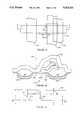
- this embodiment of the novel EEPROM cell, 101, of this invention includes a buried source region 102 and a buried drain region 103, each being buried by a relatively thick layer of dielectric 104 and 105, respectively.
- Channel region 106 is divided into two portions, a first portion 106-1 which is influenced by the third layer polycrystalline silicon 109 and which forms a select gate, and a second portion 106-2 which is influenced by floating gate 107 formed of a first layer of polycrystalline silicon and which, in turn, is influenced by control gate 108 formed of a second layer polycrystalline silicon.
- suitable dielectric layers such as thermally grown oxide are located between channel 106 and polycrystalline silicon layer 109 and polycrystalline silicon layer 107.
- suitable dielectric layers such as oxide or composite oxide/nitride are formed between the three layers of polycrystalline silicon.
- Polycrystalline metal silicide can be used in place of one or more of the polycrystalline silicon layers 108 and 109.
- a highly-doped P+ region 120 is used within channel 106-2 adjacent buried drain region 103.
- This region 120 is formed, for example, as a double diffused MOS (DMOS) region in order to establish the threshold voltage V t of the memory transistor including channel 106-2.
- DMOS double diffused MOS
- Table 1 An example of operating conditions and levels associated with the embodiment of FIG. 1b are shown in Table 1.
- High efficiency programming comes about by the ability to simultaneously create a high field region in channel 106-2 under the floating gate, which under the bias conditions of Table 1 occur near the gap between channels 106-1 and 106-2 (see above mentioned IEDM article of Kamiya for theory) while maintaining a low channel current. Since this high field causes electron injection to floating gate 107 near the source side of channel 106-2, this type of operation is termed "source-side" injection.
- This mechanism provides high efficiency, low power programming by maintaining a low channel current via word line 109 throttling by using a bias operating near channel threshold, VT p3 .
- a major attribute of this type of operation is that it allows for a high drive condition in floating gate channel 106-2 under the floating gate (in fact it thrives on it), offering high-performance read, without degrading programming performance.
- This is because the very weak drive condition on the select transistor of channel 106-1 is established via the throttling mentioned above to achieve the high fields in the vicinity of the poly 3/poly 1 gap. These fields accelerate the electrons to sufficiently energetic levels (i.e. >3.1 eV) to surmount the Si/SiO 2 interface barrier at the source side of floating gate 107.
- there is a significant vertical component to that field i.e. normal to the Si/SiO 2 surface) driving the electrons up to the surface of channel 106, and thereby assisting the injection into floating gate 107.
- a major feature of the cell of this invention is the decoupling of the select function (in this case poly 3 select transistor 110 in FIG. 1b) from the steering function (poly 2 control gate 108).
- the select function in this case poly 3 select transistor 110 in FIG. 1b
- the steering function poly 2 control gate 108.
- this allows the independent control of cell selection/drain current throttling via poly 3 word line 109 bias (biased at slightly higher than VT p3 ) and strong positive voltage coupling onto floating gate 107 (by raising poly 2 control gate 108 to a high voltage, such as about 12 volts).
- the drain voltage can be adjusted independently of steering and select transistor voltage levels, to optimize programming.
- the decoupling feature of this invention provides two important advantages, and one exciting side benefit.
- control/gate voltage is set to about 2 v, to discriminate between the logical 3 state and the logical 1/logical 2 states.
- the two options for erase operation/bias conditions shown in Table 1 stem from two different sets of considerations.
- the first option shown brings poly 2 control gate 108 to a large negative voltage, but allows poly 3 word line 109 to remain at a low voltage (e.g. 0 v to 5 v). This is desirable since the word lines and their decoders are preferably high performance, and repeated many times with a tightly pitched requirement, making high voltage word line requirements more difficult and real estate consuming to implement.
- Poly 2 control or steering gate 108 on the other hand could be common to a multiplicity of word lines (e.g. a sector consisting of 4 or more word lines), putting less demands on real estate and minimal impact to performance.
- poly 2 is used only as a steering electrode during all three operations.
- Poly 3 which is the word line connection to the X-decoder, only sees 0 V to 5 V (other than for erase option 2), and its capacitance can be made relatively small. It is relatively easy to generate +5 V and -17 V on poly 2 since both writing and erasing are slow operations relative to reading and there is no DC current drain.
- the -17 V does require high voltage PMOS in the erase decode, but the +5 V on poly 3 aids in reducing the maximum negative voltage required on poly 2 during erase.
- the second option of using high word line voltage bias for erase eliminates both of the above potential drawbacks, but burdens the high performance, tightly pitched word line/driver with high voltage requirement.
- FIG. 1d is a plan view of one embodiment of an array consisting of a plurality of cells constructed as just described with respect to FIGS. 1a-1c, and using similar reference numerals. Also shown, are channel stop isolation regions 180.
- FIG. 1e shows a block diagram of a memory array similar to that shown in the plan view of FIG. 1d which is organized by sectors, with appropriate control circuitry. Operation of one embodiment of such a memory array organized by sectors is shown in FIG. 1f. As shown in FIGS. 1e and 1f, in this embodiment sectors are formed by a single column or a group of columns having their control gate connected in common. This allows a high speed shift register to be used in place of a row decoder in order to serially shift in a whole block of column data for the word lines, with the data for each word line being contained in the shift register on completion of its serial loading.
- each sector has an associated latch for tagging that sector in preparation for an erase of a plurality of tagged sectors.
- a sector is formed in a group of four cell columns, each column being 1024 bits tall with a common control gate and an associated sector latch.
- verification of programming is performed in parallel on all to-be-programmed cells in a single column.
- Logical 0 state cells have word lines at 0 volts while logical 1 state cells have word lines at a positive voltage, such as 5 volts.
- the control gate and drain voltages are reduced to a verify level to allow for proper margin testing and the bit line current is monitored. If all of the to-be-programmed cells have been properly programmed, the bit line current will be 0 or substantially so.
- steps 1 and 2 of the above process sequence is forming horizontal strips of isolation oxide first, and then depositing P 1 and etched back in RIE to fill and planarize the horizontal grooves between adjacent strips of isolation oxide.
- step 6 Another embodiment for achieving a virtual ground cell without the use of the buried diffusion formed early in the process is now described.
- a photoresist masked arsenic source/drain implant is used, self-aligned to one edge of poly 2 after poly 1 stack formation but leaving an unimplanted region along the other edge to become the poly 3 controlled select transistor channel (see FIG. 8).
- the isolation oxide thickness formed earlier between poly 1 strips is made sufficiently thick to withstand the self-aligned poly 2/1 stack etch without exposing the substrate to pitting, but thin enough such that following this stack etch it is readily removed to expose the substrate to the source drain implant. This offers the benefit of reduced thermal drive of the arsenic junction laterally facilitating scaling.
- the remainder of the process steps of this embodiment follows the prior embodiment.
- novel cell of this invention offers the following benefits.
- a second array embodiment is similar to that of FIG. 1d but uses the cell embodiment shown in FIG. 1b, to form a row oriented sector architecture, is shown in FIG. 1g.
- a sector consists of a group of rows, four in this example, which are erased together.
- Erase uses option 2 of Table I, for this row oriented sector architecture, bringing all the poly 3 word lines of a sector to high voltage.
- the poly 2 steering gate is common to a group of N sectors where N can range from 1 to the full size of the memory array.
- the BN+ columns can alternatively continuously span the full length of the array or be broken down into a collection of shorter length, local columns. These connect to a global (full array length) column through a select transistor driven by an additional level of decoding.
- the local columns can range from 1 to N sectors.
- the preferred embodiment is to have local columns span the same number of sectors as the poly 2 steering gate.
- a preferred number of sectors, N, spanned by local columns and poly 2 steering is around 8. This is because if N is much smaller than 8, the area overhead for local column section devices and poly 2 steering gate routing is high in relation to the area of arrayed cells, while if N is much larger than 8, the benefits of having localized columns and poly 2 steering diminish.
- These benefits are: (1) reduced bit line capacitance improving read performance; (2) reduced repetitive exposure on unselected sectors to the raised voltage conditions on drains and steering electrodes when programming one sector within the N-sector group, and associated potential disturb phenomena; and (3) increased confinement of array related failures thereby increasing the efficiency of replacing such failures.
- Read, program and unselected conditions are as described in Table I, during read or program.
- the poly 3 word line in the selected row within the selected sector is turned on, 5 volts for read and approximately 1 volt for programming.
- the drain to source bias conditions are applied to the columns, approximately 5 volts for program and approximately 1.0-1.5 volts for read.
- alternate bits in a selected row are programmed simultaneously, thereby permitting all bits in a selected row to be programmed utilizing two programming operations.
- alternate bits in a selected row are read (or verified) simultaneously, thereby permitting all bits in a selected row to be read (or verified) utilizing two read (or verify) operations.
- the row oriented sector architecture and array operation is much more conventional than the column oriented sector of the first embodiment, and consequently operates in a more traditional manner. Both embodiments share the intrinsic low power capability of this invention, but the row oriented sector embodiment requires, in addition, a full complement of data registers to support massively parallel write and verify features.
- FIG. 2a shows an alternative array embodiment of this invention which does not utilize buried diffusion regions.
- source region 102 and drain region 103 are formed in a conventional manner and not buried by a thick dielectric layer as is the case in the embodiment of FIG. 1b.
- a plurality of memory cells are shown in FIG. 2a along a cross section of a typical array structure, with elements of one such cell numbered using reference numerals corresponding to similar structure in FIG. 1b.
- Table 3 depicts an example of the operating conditions appropriate for the embodiment of FIG. 2a.
- This a more traditional cell approach compared to the buried diffusion cell, with source/drain diffusions formed after all the polycrystalline silicon structures are formed. It requires one drain contact to metal bit line for every 2 cells, making it approximately 30% to 50% larger than the buried diffusion cell with similar layout rules.
- this alternative embodiment offers the same benefits as listed above for the buried diffusion embodiment of FIG. 1b.
- FIG. 2b is a plan view of one embodiment of an array of memory cells constructed as described above with reference to FIG. 2a.
- FIG. 2c is an equivalent circuit diagram depicting the organization of such a memory array in sectors, with appropriate operating conditions and voltages shown.
- the preferred embodiment for a sector organized array uses two word lines which straddle a source line as part of a sector, along with their associated poly 2 steering gates and source line.
- a full sector consists of some multiple of such pairing (e.g. 2 such pairs or 4 word lines, each word line containing 128 bytes and overhead cells, and straddling two source lines, constitute one sector).
- the steering lines are connected together within a sector as are the source lines (i.e. a sector which consists of row lines grouped together respectively and driven by common drivers).
- the embodiment described here confines the write operation to the sector being written to, while the bit line bias conditions (2.5 v during read and approximately 5 v possible during write) are non-disturbing to the cells because the bias is applied to the select transistor side of the cell and not to the floating gate side.
- the bit line In a two state cell, to write the cell to a logical one, the bit line is held at zero volts, causing the cell to program via source-side injection. Conversely, to inhibit writing, the bit line is held high (typically about 5 volts), thereby cutting off the channel, leaving the cell in the erased state.
- Sector erase takes place by tagging the selected sector and raising the associated row lines to a sufficiently high voltage to erase the floating gates to their required erased levels.
- FIG. 3 is a graph depicting the gate current into poly 1 gate 107 of FIG. 1b (which is not floating in the FIG. 3 test device to allow this measurement to be made) as a function of poly 1 gate voltage (V poly 1) while keeping the select transistor 110 V p2 at just above its threshold.
- V poly 1 gate voltage V poly 1 gate voltage
- a starting substrate is used, for example a P type substrate (or a P type well region within an N type substrate).
- a layer of oxide is formed, followed by a layer of silicon nitride.
- the layer of silicon nitride is then patterned in order to expose those areas in which N+ source and drain regions are to be formed.
- the N+ source and drain regions are then formed, for example, by ion implantation of arsenic to a concentration of approximately 1 ⁇ 10 20 cm-3.
- the wafer is then oxidized in order to form oxide layers 104 and 105 in order to cause source and drain regions 102 and 103 to become "buried". Rather, the source and drain regions are formed after all polycrystalline silicon layers are formed, in a conventional manner. Note that for the embodiment of FIG. 2a, this oxidation step is not utilized, as the source and drain regions are not "buried”.
- the remaining portion of the nitride mask is then removed, and the oxide overlying channel regions 106-1 and 106-2 is removed.
- a new layer of gate oxide overlying channel regions 106-1 and 106-2 is formed, for example to a thickness within the range of 150 ⁇ to 300 ⁇ and implanted to the desired threshold (e.g. approximately -1 v to +1 v).
- Polycrystalline silicon is then formed on the wafer and patterned in order to form floating gate regions 107. If desired, the polycrystalline silicon layer is patterned in horizontal strips (per the orientation of FIG. 1a), with its horizontal extent patterned at the same time as the patterning of the second layer of polycrystalline silicon, as will be now described. Following the formation polycrystalline silicon layer 107 at this time, a layer of oxide or oxide/nitride dielectric is formed over the remaining portions of polycrystalline silicon layer 107.
- a second layer of polycrystalline silicon 108 is then formed and doped to a desired conductivity, for example 30 ohms/square.
- the second layer of polycrystalline silicon is then patterned into vertical strips (again, per the orientation of FIG. 1a). If the horizontal extent of polycrystalline silicon layer 107 was not earlier defined, this pattern step is also used to remove the layer of dielectric between the first and second layers of polycrystalline silicon in those areas where the first layer of polycrystalline silicon is to be patterned simultaneously with the patterning of the second layer of polycrystalline silicon.
- an additional layer of dielectric is formed on the wafer to form the gate dielectric above channel region 106-1, and above any other areas in the silicon substrate to which the third layer of polycrystalline silicon is to make a gate.
- the third layer of polycrystalline silicon is for a transistor (ranging from ⁇ 200 ⁇ to 500 ⁇ in thickness) then formed and doped to appropriate conductivity, for example 20 ohms/square.
- Polycrystalline silicon layer 109 is then patterned in order to form word line 109.
- polycrystalline silicon layer 107 is patterned to form horizontal stripes and channel stop dopants (e.g. boron) are implanted into the exposed areas therebetween in order to form high threshold channel stop regions between adjacent rows of a memory array.
- channel stop dopants e.g. boron
- the thickness of the gate dielectric between channel 106-2 and polycrystalline silicon floating gate 107 can range from approximately 150 angstroms or less to approximately 300 angstroms or more, depending on performance tradeoffs. For increased drive for reading, a thinner gate dielectric is desired while for increased coupling between polycrystalline and silicon control gate 108 and floating gate 107 (helpful during programming) a thicker gate dielectric is desired.
- FIG. 5 is a two-poly embodiment in which programming occurs by taking drain 303 high, for example about 10 V while raising control gate 308 just sufficiently so as to turn on select transistor 310. Since this V CG voltage can vary from one device to another it is possible to achieve the optimum injection conditions by keeping V CG at about 3 V while raising source (virtual ground) 302 in a sawtooth fashion from about 0 to 3 volts and back to 0 again, with a period on the order approximately 1 microsecond.
- a programming efficiency implant 330 (shown in dotted line) is introduced at the source side. To read the device, its source is 0 V, drain is approximately 1.0 v and approximately 4.5-5 v. To erase we employ poly 1-poly 2 tunneling between floating gate 307 in word line 308 at the tunneling zone, consisting of one or more of the floating gate edges, sidewall, corners of the top edge, portions of the top and portions of the bottom, of floating gate 307, associated with a tunnel oxide (400 ⁇ -700 ⁇ ).
- V CG approximately 12-22 V
- V D 0 V
- V S 0 V
- a capacitive decoupling dielectric (approximately 1500 to 2000 ⁇ thick) 340 is formed on top of poly 1 to reduce the capacitance between poly 1 and poly 2.
- a high electrical field region is created in the channel far away from the reverse field region located in conventional devices near the drain. This is achieved, for example, by utilizing region 330 of increased doping concentration at the boundary between channels 306-1 and 306-2 under floating gate 307.
- the width of region 330 is on the order of 0.1 microns. A larger dimension for region 330 can be counterproductive, reducing the select transistor drive with no gain in efficiency.
- FIG. 4 depicts the electrical field distribution along channels 306-1 and 306-2 in structures with and without P+ doped region 330.
- the electron injection can take place in the high field region near drain 303. Because of the vertical field reversal region near drain 303, the resultant injection efficiency is reduced.
- the injection takes place in the high field region located at region 330, far away from the field reversal region. Because of this, increased injection efficiency is achieved.
- This array permits floating gate 307 to completely overlap the buried N + diffusion in a dedicated source arrangement, eliminating this alignment sensitivity.
- this array requires an extra isolation spacing adjacent to the BN+ to prevent the poly 1 extension beyond BN+ in the direction away from channel 306-2 to form a transistor in the neighboring cell.
- a channel stop isolation is used between adjacent cells, plus a self-aligned stacked etch to simultaneously delineate poly 2 and poly 1. This is difficult to do without pitting the substrate as well as the exposed BN+ when etching the exposed poly 1 between adjacent cells. This is especially difficult to avoid when etching the decoupling oxide (1500-2000 ⁇ thick on top of poly 1 in order to expose poly 1, since the substrate unprotected by poly 1 also becomes exposed, so that when poly 1 is etched, the substrate in those regions becomes pitted.
- FIG. 6 is a cross-sectional view of alternative embodiment of a two poly cell, using source side injection for programming, aided by strong coupling to buried N+ drain 403, which acts also as a second control gate.
- Erase is by Fowler-Nordheim tunneling to channel 406 through a small thinned oxide region, formed for example to a thickness of about 100 ⁇ , by utilizing a thin polyspacer.
- These process steps would be as follows: Once the drain oxide is formed (i.e. the oxide above drain 403), a first layer of poly, (approximately 2000 ⁇ to 4000 ⁇ thick) is deposited and a thin nitride dielectric is deposited on top.
- These layers are then etched using a poly 1 mask to delineate the lateral extent (as shown in FIG. 6) of the poly 1.
- a second layer of nitride is then deposited and anisotropically etched back to underlying oxide, leaving the initial nitride layer on top of poly 1 plus nitride spacers along the poly 1 sidewalls. This protects the poly 1 sidewall from subsequent oxidation, allowing electrical contact to be made as later described.
- the exposed oxide layer over the channel portion of the substrate is then stripped and regrown to the 100 ⁇ thickness required for tunneling, while a photoresist masked pattern protects oxide over the exposed, BN+ side of the poly 1 from being stripped.
- the nitride layers surrounding poly 1 prevents oxide from forming on that poly.
- the thin nitride is then etched off using a highly selective etch which does not attack or degrade the 100 ⁇ tunnel oxide (e.g. hot phosphoric or plasma etch).
- This is followed by a second poly deposition which electrically contacts the first poly on its top surface and its sidewalls.
- This structure is then etched using an anisotropic poly-silicon etch, with etch being terminated with the re-exposure of the oxide layers over substrate beneath the second deposited poly layer. This completes the formation of the poly 1 floating gate stripe shown in FIG. 6.
- the remaining process is similar to that of the second embodiment.
- programming is from hot channel electrons injected from grounded source diffusion 402 with drain 403 held at about +8 v and fixed control gate of around 1.5 v.
- programming is performed by hot channel electrons from source diffusion 402 utilizing a sawtooth control gate voltage ranging from 0 volts to a peak voltage approximately 3 volts, as described previously for the second embodiment.
- the poly 2 word line 408 will carry the +5 volts during read and the -22 volts during erase, thereby requiring an x-decoder capable of serving this purpose.
- Coupling considerations require that C P2P1 >C P1D , which is unfavorable for programming. Therefore the cell must be optimized for balancing erase against programming by adjusting oxide thicknesses and floating gate threshold to the optimum print. There is less of a problem with pitting the field regions between cells in the poly 1 direction (because poly 1--poly 2 oxide or ONO is thin). This may obviate the need for the additional thick oxide field region described for the second embodiment. However, there is the additional process complexity of forming the thin oxide region and extra space needed to place this thin oxide region sufficiently far from the source diffusion.
- a number of alternative methods are possible to program the source side injection cells described in the previous embodiments. Strong capacitive coupling (for example, using thin ONO) is required in the second and third embodiments between poly 2 and drain and between poly 2 and poly 1 respectively for programming.
- V D at 5 to 7 v
- V S 0
- the control gate voltage V CG is raised to just turn on the control gate channel
- V p2 is on the order of about 12 volts or more.
- the source body effect is used to advantage.
- control gate is brought to a value greater than the voltage required to just turn on the channel (e.g., approximately one volt above) and a pull-down circuit is used (e.g., a high impedance resistor or a current sink) for providing approximately 1 ⁇ A current flow via source debiasing.
- a pull-down circuit e.g., a high impedance resistor or a current sink
- the control gate voltage V CG can be operated in a sawtooth fashion from between 0 volts to about +3 volts, as mentioned previously with respect to European patent application serial number 89312799.3.
Abstract
Description
                                  TABLE 1
__________________________________________________________________________
State Table & Operating Conditions (FIG. 1b)
                Poly 3
                     Poly 2  Drain
                                  Source
Mode of         (Word
                     (Steering
                             (BN &
                                  & (BN
Operation       line)
                     Gate)   Drain)
                                  Source)
__________________________________________________________________________
  R STANDBY     0 v  0 v     1.0 v or
                                  1.0 v or
  E                          0 v  0 v
R L READ SELECTED
                5 v  0 v     1.0 v or
                                  0 v or
E A                          0 v  1.0 v
A T READ UNSELECTED
                5 v  0 v     1.0 v
                                  1.0 v
D E
  D
E R Erase Unselected
                5 v  0 v     0 v  0 v
R E
A L
S A
E T ERASE Option 1
                5 v  -10 to -17 v
                             0 v  0 v
  E or Option 2 12-22 v
                     0 v     0 v  0 v
  D
P R PROGRAM     ˜1.5 v
                     14-20 v 5-7 v
                                  0 v
R E SELECTED
O L
G A
R T PROGRAM     0 v  14-20 v 5-7 v
                                  0 v
A E UNSELECTED  ˜1.5 V
                     14- 20 v
                             5-7 v
                                  5-7 v
M D             0 v  14-20 v 0 v  0 v
__________________________________________________________________________
TABLE 2 ______________________________________READ PASS 1PASS 2 STATE [Ref. = 0 v] [Ref. = 2] ______________________________________ 1 Hi Hi 2Lo Hi 3 Lo Lo ______________________________________
                                  TABLE 3
__________________________________________________________________________
State Table & Operating Conditions (FIG. 2a)
                Poly 3
                     Poly 2
Node            (Word
                     (Steering
Operation       line)
                     Gate)   Drain Source
__________________________________________________________________________
R R STANDBY     0 v  0 v     Don't care
                                   0 v
E E READ SELECTED
                5 v  0 v     2.5 v 0 v
A L READ UNSELECTED
                5 v  0 v     Don't care
                                   0 v
D A
  T
  E
  D
E R STANDBY     0 v  0 v     0 v   0 v
R E
A L
S A
E T ERASE Option 1
                12 v-22 v
                     0 v     0 v   0 v
  E
  D Option 2    5 v  -10 v to -12 v
                             0 v   0 v
P R PROGRAM     ˜1.0 v
                     14-20   0 v   5 v-8 v
R E SELECTED
O L
G A
R T PROGRAM     0 v  14-20   0 v   5 v-8 v
A E UNSELECTED  ˜1.0 v
                     14-20   5 v   5 v-8 v
M D             0 v  14-20   5 v   5 v-8 v
__________________________________________________________________________
Claims (42)
Priority Applications (17)
| Application Number | Priority Date | Filing Date | Title |
|---|---|---|---|
| US07/820,364 US5313421A (en) | 1992-01-14 | 1992-01-14 | EEPROM with split gate source side injection |
| PCT/US1993/000265 WO1993014521A1 (en) | 1992-01-14 | 1993-01-12 | Eeprom with split gate source side injection |
| JP51262893A JP3738030B2 (en) | 1992-01-14 | 1993-01-12 | Method for forming a semiconductor structure |
| US08/193,707 US5776810A (en) | 1992-01-14 | 1994-02-09 | Method for forming EEPROM with split gate source side injection |
| US08/607,951 US5712180A (en) | 1992-01-14 | 1996-02-28 | EEPROM with split gate source side injection |
| US08/639,128 US5847996A (en) | 1992-01-14 | 1996-04-26 | Eeprom with split gate source side injection |
| US08/910,947 US6222762B1 (en) | 1992-01-14 | 1997-08-07 | Multi-state memory |
| US08/908,744 US5883409A (en) | 1992-01-14 | 1997-08-07 | EEPROM with split gate source side injection |
| US09/065,409 US5910925A (en) | 1992-01-14 | 1998-04-23 | EEPROM with split gate source side injection |
| US09/065,512 US5910915A (en) | 1992-01-14 | 1998-04-23 | EEPROM with split gate source side injection |
| US09/207,956 US6002152A (en) | 1992-01-14 | 1998-12-09 | EEPROM with split gate source side injection with sidewall spacers |
| US09/687,986 US6317363B1 (en) | 1992-01-14 | 2000-10-13 | Multi-state memory |
| US09/688,068 US6275419B1 (en) | 1992-01-14 | 2000-10-13 | Multi-state memory |
| US09/688,061 US6317364B1 (en) | 1992-01-14 | 2000-10-13 | Multi-state memory |
| US10/013,592 US6856546B2 (en) | 1992-01-14 | 2001-11-13 | Multi-state memory |
| US10/225,105 US6954381B2 (en) | 1992-01-14 | 2002-08-20 | EEPROM with split gate source side injection with sidewall spacers |
| US12/499,581 US7898868B2 (en) | 1992-01-14 | 2009-07-08 | Multi-state memory |
Applications Claiming Priority (1)
| Application Number | Priority Date | Filing Date | Title |
|---|---|---|---|
| US07/820,364 US5313421A (en) | 1992-01-14 | 1992-01-14 | EEPROM with split gate source side injection |
Related Child Applications (2)
| Application Number | Title | Priority Date | Filing Date |
|---|---|---|---|
| US08/193,707 Division US5776810A (en) | 1992-01-14 | 1994-02-09 | Method for forming EEPROM with split gate source side injection |
| US08/193,707 Continuation US5776810A (en) | 1992-01-14 | 1994-02-09 | Method for forming EEPROM with split gate source side injection |
Publications (1)
| Publication Number | Publication Date |
|---|---|
| US5313421A true US5313421A (en) | 1994-05-17 |
Family
ID=25230576
Family Applications (5)
| Application Number | Title | Priority Date | Filing Date |
|---|---|---|---|
| US07/820,364 Expired - Lifetime US5313421A (en) | 1992-01-14 | 1992-01-14 | EEPROM with split gate source side injection |
| US08/193,707 Expired - Lifetime US5776810A (en) | 1992-01-14 | 1994-02-09 | Method for forming EEPROM with split gate source side injection |
| US08/639,128 Expired - Lifetime US5847996A (en) | 1992-01-14 | 1996-04-26 | Eeprom with split gate source side injection |
| US09/065,512 Expired - Lifetime US5910915A (en) | 1992-01-14 | 1998-04-23 | EEPROM with split gate source side injection |
| US09/065,409 Expired - Lifetime US5910925A (en) | 1992-01-14 | 1998-04-23 | EEPROM with split gate source side injection |
Family Applications After (4)
| Application Number | Title | Priority Date | Filing Date |
|---|---|---|---|
| US08/193,707 Expired - Lifetime US5776810A (en) | 1992-01-14 | 1994-02-09 | Method for forming EEPROM with split gate source side injection |
| US08/639,128 Expired - Lifetime US5847996A (en) | 1992-01-14 | 1996-04-26 | Eeprom with split gate source side injection |
| US09/065,512 Expired - Lifetime US5910915A (en) | 1992-01-14 | 1998-04-23 | EEPROM with split gate source side injection |
| US09/065,409 Expired - Lifetime US5910925A (en) | 1992-01-14 | 1998-04-23 | EEPROM with split gate source side injection |
Country Status (3)
| Country | Link |
|---|---|
| US (5) | US5313421A (en) |
| JP (1) | JP3738030B2 (en) |
| WO (1) | WO1993014521A1 (en) |
Cited By (400)
| Publication number | Priority date | Publication date | Assignee | Title |
|---|---|---|---|---|
| US5495441A (en) * | 1994-05-18 | 1996-02-27 | United Microelectronics Corporation | Split-gate flash memory cell |
| US5544103A (en) * | 1992-03-03 | 1996-08-06 | Xicor, Inc. | Compact page-erasable eeprom non-volatile memory |
| US5644532A (en) * | 1992-09-08 | 1997-07-01 | National Semiconductor Corporation | Method for programming a cell in a source-coupling, split-gate, virtual ground flash EEPROM array |
| US5712180A (en) * | 1992-01-14 | 1998-01-27 | Sundisk Corporation | EEPROM with split gate source side injection |
| US5776810A (en) * | 1992-01-14 | 1998-07-07 | Sandisk Corporation | Method for forming EEPROM with split gate source side injection |
| US5870335A (en) * | 1997-03-06 | 1999-02-09 | Agate Semiconductor, Inc. | Precision programming of nonvolatile memory cells |
| EP0902438A1 (en) * | 1997-09-09 | 1999-03-17 | Interuniversitair Micro-Elektronica Centrum Vzw | Methods of erasing a memory device and a method of programming a memory device for low-voltage and low-power applications |
| US5915178A (en) * | 1997-12-08 | 1999-06-22 | Taiwan Semiconductor Manufacturing Company, Ltd. | Method for improving the endurance of split gate flash EEPROM devices via the addition of a shallow source side implanted region |
| US5946234A (en) * | 1997-12-18 | 1999-08-31 | Advanced Micro Devices, Inc. | Constant current source programming of electrically programmable memory arrays |
| US5970341A (en) * | 1997-12-11 | 1999-10-19 | Taiwan Semiconductor Manufacturing Company, Ltd. | Method for forming vertical channels in split-gate flash memory cell |
| US6002614A (en) * | 1991-02-08 | 1999-12-14 | Btg International Inc. | Memory apparatus including programmable non-volatile multi-bit memory cell, and apparatus and method for demarcating memory states of the cell |
| US6017795A (en) * | 1998-05-06 | 2000-01-25 | Taiwan Semiconductor Manufacturing Company | Method of fabricating buried source to shrink cell dimension and increase coupling ratio in split-gate flash |
| US6091633A (en) * | 1999-08-09 | 2000-07-18 | Sandisk Corporation | Memory array architecture utilizing global bit lines shared by multiple cells |
| US6103573A (en) * | 1999-06-30 | 2000-08-15 | Sandisk Corporation | Processing techniques for making a dual floating gate EEPROM cell array |
| US6151248A (en) * | 1999-06-30 | 2000-11-21 | Sandisk Corporation | Dual floating gate EEPROM cell array with steering gates shared by adjacent cells |
| US6222762B1 (en) | 1992-01-14 | 2001-04-24 | Sandisk Corporation | Multi-state memory |
| US6282145B1 (en) | 1999-01-14 | 2001-08-28 | Silicon Storage Technology, Inc. | Array architecture and operating methods for digital multilevel nonvolatile memory integrated circuit system |
| US6353554B1 (en) | 1995-02-27 | 2002-03-05 | Btg International Inc. | Memory apparatus including programmable non-volatile multi-bit memory cell, and apparatus and method for demarcating memory states of the cell |
| US6396742B1 (en) | 2000-07-28 | 2002-05-28 | Silicon Storage Technology, Inc. | Testing of multilevel semiconductor memory |
| US6438027B1 (en) * | 1999-10-07 | 2002-08-20 | Hyundai Electronic Industries Co., Ltd. | Nonvolatile memory, cell array thereof, and method for sensing data therefrom |
| US6462986B1 (en) | 1995-10-06 | 2002-10-08 | Silicon Storage Technology, Inc. | Integrated circuit for storage and retrieval of multiple digital bits per nonvolatile memory cell |
| DE19534921C2 (en) * | 1994-09-27 | 2002-10-31 | Hyundai Electronics Ind | Process for the production of EEPROM flash cells with buried bit lines |
| US6487116B2 (en) | 1997-03-06 | 2002-11-26 | Silicon Storage Technology, Inc. | Precision programming of nonvolatile memory cells |
| US6493269B1 (en) | 2001-05-31 | 2002-12-10 | Sandisk Corporation | Dual cell reading and writing technique |
| US6501680B1 (en) | 1999-10-07 | 2002-12-31 | Hyundai Electronics Industries Co., Ltd. | Nonvolatile memory, cell array thereof, and method for sensing data therefrom |
| US6512263B1 (en) | 2000-09-22 | 2003-01-28 | Sandisk Corporation | Non-volatile memory cell array having discontinuous source and drain diffusions contacted by continuous bit line conductors and methods of forming |
| WO2003015173A2 (en) | 2001-08-08 | 2003-02-20 | Sandisk Corporation | Floating gate memory array and methods of forming |
| US6532172B2 (en) | 2001-05-31 | 2003-03-11 | Sandisk Corporation | Steering gate and bit line segmentation in non-volatile memories |
| US20030052360A1 (en) * | 1992-01-14 | 2003-03-20 | Guterman Daniel C. | EEPROM with split gate source side injection with sidewall spacers |
| US20030109093A1 (en) * | 2001-10-31 | 2003-06-12 | Eliyahou Harari | Multi-state non-volatile integrated circuit memory systems that employ dielectric storage elements |
| US20030161185A1 (en) * | 2002-02-28 | 2003-08-28 | Sandisk Corporation | Method and system for efficiently reading and programming of dual cell memory elements |
| US6639309B2 (en) | 2002-03-28 | 2003-10-28 | Sandisk Corporation | Memory package with a controller on one side of a printed circuit board and memory on another side of the circuit board |
| US20030209751A1 (en) * | 2001-05-18 | 2003-11-13 | Sandisk Corporation | Floating gate memory cells utilizing substrate trenches to scale down their size |
| US20040000688A1 (en) * | 2001-05-18 | 2004-01-01 | Sandisk Corporation | Non-volatile memory cells utilizing substrate trenches |
| US20040060031A1 (en) * | 2002-09-24 | 2004-03-25 | Sandisk Corporation | Highly compact non-volatile memory and method thereof |
| US20040057318A1 (en) * | 2002-09-24 | 2004-03-25 | Sandisk Corporation | Non-volatile memory and method with reduced bit line crosstalk errors |
| US20040057285A1 (en) * | 2002-09-24 | 2004-03-25 | Sandisk Corporation | Non-volatile memory and method with reduced neighboring field errors |
| US6714449B2 (en) | 2000-09-27 | 2004-03-30 | Sandisk Corporation | Sense amplifier suitable for analogue voltage levels |
| US20040070021A1 (en) * | 2002-10-09 | 2004-04-15 | Yuan Jack H. | Flash memory array with increased coupling between floating and control gates |
| US20040109357A1 (en) * | 2002-09-24 | 2004-06-10 | Raul-Adrian Cernea | Non-volatile memory and method with improved sensing |
| US20040145952A1 (en) * | 2003-01-28 | 2004-07-29 | Jian Chen | Non-volatile semiconductor memory with large erase blocks storing cycle counts |
| US20040174744A1 (en) * | 2001-02-26 | 2004-09-09 | Geoffrey Gongwer | Non-volatile memory with improved programming and method therefor |
| US20040237010A1 (en) * | 1992-05-20 | 2004-11-25 | Auclair Daniel L. | Soft errors handling in EEPROM devices |
| US20040232496A1 (en) * | 2003-05-21 | 2004-11-25 | Jian Chen | Use of voids between elements in semiconductor structures for isolation |
| US20040240269A1 (en) * | 2001-09-17 | 2004-12-02 | Raul-Adrian Cernea | Latched programming of memory and method |
| US20040257877A1 (en) * | 2003-06-20 | 2004-12-23 | Raul-Adrian Cernea | Source controlled operation of non-volatile memories |
| US6839875B2 (en) * | 1996-10-18 | 2005-01-04 | Micron Technology, Inc. | Method and apparatus for performing error correction on data read from a multistate memory |
| US20050003616A1 (en) * | 2003-06-20 | 2005-01-06 | Jeffrey Lutze | Self aligned non-volatile memory cell and process for fabrication |
| US20050057965A1 (en) * | 2003-09-17 | 2005-03-17 | Raul-Adrian Cernea | Non-volatile memory and method with bit line coupled compensation |
| US20050072999A1 (en) * | 2003-10-06 | 2005-04-07 | George Matamis | Bitline direction shielding to avoid cross coupling between adjacent cells for NAND flash memory |
| US20050073884A1 (en) * | 2003-10-03 | 2005-04-07 | Gonzalez Carlos J. | Flash memory data correction and scrub techniques |
| US6888758B1 (en) | 2004-01-21 | 2005-05-03 | Sandisk Corporation | Programming non-volatile memory |
| US6891753B2 (en) | 2002-09-24 | 2005-05-10 | Sandisk Corporation | Highly compact non-volatile memory and method therefor with internal serial buses |
| US6894930B2 (en) | 2002-06-19 | 2005-05-17 | Sandisk Corporation | Deep wordline trench to shield cross coupling between adjacent cells for scaled NAND |
| US6897522B2 (en) | 2001-10-31 | 2005-05-24 | Sandisk Corporation | Multi-state non-volatile integrated circuit memory systems that employ dielectric storage elements |
| US20050141312A1 (en) * | 2003-12-30 | 2005-06-30 | Sinclair Alan W. | Non-volatile memory and method with non-sequential update block management |
| US20050144367A1 (en) * | 2003-12-30 | 2005-06-30 | Sinclair Alan W. | Data run programming |
| US20050144363A1 (en) * | 2003-12-30 | 2005-06-30 | Sinclair Alan W. | Data boundary management |
| US20050144358A1 (en) * | 2003-12-30 | 2005-06-30 | Conley Kevin M. | Management of non-volatile memory systems having large erase blocks |
| US20050144357A1 (en) * | 2003-12-30 | 2005-06-30 | Sinclair Alan W. | Adaptive metablocks |
| US20050160217A1 (en) * | 2003-12-31 | 2005-07-21 | Gonzalez Carlos J. | Flash memory system startup operation |
| US20050162923A1 (en) * | 2004-01-27 | 2005-07-28 | Guterman Daniel C. | Charge packet metering for coarse/fine programming of non-volatile memory |
| US20050162924A1 (en) * | 2004-01-27 | 2005-07-28 | Guterman Daniel C. | Variable current sinking for coarse/fine programming of non-volatile memory |
| US20050162916A1 (en) * | 2004-01-27 | 2005-07-28 | Guterman Daniel C. | Efficient verification for coarse/fine programming of non-volatile memory |
| US20050162927A1 (en) * | 2002-06-19 | 2005-07-28 | Henry Chien | Deep wordline trench to shield cross coupling between adjacent cells for scaled NAND |
| US6940753B2 (en) | 2002-09-24 | 2005-09-06 | Sandisk Corporation | Highly compact non-volatile memory and method therefor with space-efficient data registers |
| US20050199939A1 (en) * | 2004-03-12 | 2005-09-15 | Lutze Jeffrey W. | Self aligned non-volatile memory cells and processes for fabrication |
| US20050237814A1 (en) * | 2004-04-23 | 2005-10-27 | Sandisk Corporation | Non-volatile memory and control with improved partial page program capability |
| US20050248988A1 (en) * | 2004-05-05 | 2005-11-10 | Guterman Daniel C | Boosting to control programming of non-volatile memory |
| US20050251617A1 (en) * | 2004-05-07 | 2005-11-10 | Sinclair Alan W | Hybrid non-volatile memory system |
| US20050248989A1 (en) * | 2004-05-05 | 2005-11-10 | Guterman Daniel C | Bitline governed approach for program control of non-volatile memory |
| EP1164596A3 (en) * | 2000-06-12 | 2005-11-16 | Sony Corporation | Memory system and programming method thereof |
| US20050268025A1 (en) * | 2004-05-27 | 2005-12-01 | Peter Smith | Configurable ready/busy control |
| US20050280030A1 (en) * | 2003-03-28 | 2005-12-22 | Au Optronics Corp. | Dual gate layout for thin film transistor |
| US6980471B1 (en) | 2004-12-23 | 2005-12-27 | Sandisk Corporation | Substrate electron injection techniques for programming non-volatile charge storage memory cells |
| US20060031593A1 (en) * | 2004-08-09 | 2006-02-09 | Sinclair Alan W | Ring bus structure and its use in flash memory systems |
| US20060034121A1 (en) * | 2003-09-17 | 2006-02-16 | Shahzad Khalid | Non-volatile memory and method with bit line compensation dependent on neighboring operating modes |
| US20060039196A1 (en) * | 2003-10-03 | 2006-02-23 | Gorobets Sergey A | Corrected data storage and handling methods |
| US20060050562A1 (en) * | 2002-09-24 | 2006-03-09 | Raul-Adrian Cernea | Non-volatile memory and method with improved sensing |
| US20060067105A1 (en) * | 2004-09-28 | 2006-03-30 | Advanced Micro Devices, Inc | Control of memory devices possessing variable resistance characteristics |
| US20060067181A1 (en) * | 1999-05-08 | 2006-03-30 | Samsung Electronics Co., Ltd | Recording medium for storing linking type information and method of processing defective area using the same |
| US20060106972A1 (en) * | 2004-11-15 | 2006-05-18 | Gorobets Sergey A | Cyclic flash memory wear leveling |
| US20060104120A1 (en) * | 2004-11-16 | 2006-05-18 | Hemink Gerrit J | High speed programming system with reduced over programming |
| US20060110880A1 (en) * | 2004-11-23 | 2006-05-25 | Yuan Jack H | Self-aligned trench filling with high coupling ratio |
| US20060108647A1 (en) * | 2004-11-23 | 2006-05-25 | Yuan Jack H | Self-aligned trench filling for narrow gap isolation regions |
| US20060120165A1 (en) * | 2004-11-16 | 2006-06-08 | Hemink Gerrit J | Faster programming of higher level states in multi-level cell flash memory |
| US20060126393A1 (en) * | 2004-12-14 | 2006-06-15 | Yan Li | Data recovery methods in multi-state memory after program fail |
| US20060126394A1 (en) * | 2004-12-14 | 2006-06-15 | Yan Li | Multi-state memory having data recovery after program fail |
| US20060134864A1 (en) * | 2004-12-22 | 2006-06-22 | Masaaki Higashitani | Multi-thickness dielectric for semiconductor memory |
| US20060136656A1 (en) * | 2004-12-21 | 2006-06-22 | Conley Kevin M | System and method for use of on-chip non-volatile memory write cache |
| US20060136655A1 (en) * | 2004-12-16 | 2006-06-22 | Gorobets Sergey A | Cluster auto-alignment |
| US20060134845A1 (en) * | 2004-12-22 | 2006-06-22 | Tuan Pham | Low-voltage, multiple thin-gate oxide and low-resistance gate electrode |
| US20060140007A1 (en) * | 2004-12-29 | 2006-06-29 | Raul-Adrian Cernea | Non-volatile memory and method with shared processing for an aggregate of read/write circuits |
| US20060155921A1 (en) * | 2004-12-16 | 2006-07-13 | Gorobets Sergey A | Non-volatile memory and method with multi-stream update tracking |
| US20060155922A1 (en) * | 2004-12-16 | 2006-07-13 | Gorobets Sergey A | Non-volatile memory and method with improved indexing for scratch pad and update blocks |
| US20060155920A1 (en) * | 2004-12-16 | 2006-07-13 | Smith Peter J | Non-volatile memory and method with multi-stream updating |
| US20060161728A1 (en) * | 2005-01-20 | 2006-07-20 | Bennett Alan D | Scheduling of housekeeping operations in flash memory systems |
| US20060158935A1 (en) * | 2002-09-24 | 2006-07-20 | Chan Siu L | Method for compensated sensing in non-volatile memory |
| US20060161724A1 (en) * | 2005-01-20 | 2006-07-20 | Bennett Alan D | Scheduling of housekeeping operations in flash memory systems |
| US20060161722A1 (en) * | 2004-12-16 | 2006-07-20 | Bennett Alan D | Scratch pad block |
| US20060158947A1 (en) * | 2002-09-24 | 2006-07-20 | Chan Siu L | Reference sense amplifier for non-volatile memory |
| US20060203545A1 (en) * | 2002-09-24 | 2006-09-14 | Raul-Adrian Cernea | Memory Sensing Circuit and Method for Low Voltage Operation |
| US20060209592A1 (en) * | 2005-03-16 | 2006-09-21 | Yan Li | Non-volatile memory and method with power-saving read and program-verify operations |
| US20060221694A1 (en) * | 2005-04-01 | 2006-10-05 | Raul-Adrian Cernea | Non-volatile memory and method with control gate compensation for source line bias errors |
| US20060221704A1 (en) * | 2005-04-01 | 2006-10-05 | Yan Li | Use of data latches in cache operations of non-volatile memories |
| US20060221697A1 (en) * | 2005-04-01 | 2006-10-05 | Yan Li | Use of data latches in multi-phase programming of non-volatile memories |
| US20060221693A1 (en) * | 2005-04-01 | 2006-10-05 | Raul-Adrian Cernea | Non-volatile memory and method with compensation for source line bias errors |
| US20060239080A1 (en) * | 2005-04-01 | 2006-10-26 | Yan Li | Method for Non-Volatile Memory with Managed Execution of Cached Data |
| US7173863B2 (en) | 2004-03-08 | 2007-02-06 | Sandisk Corporation | Flash controller cache architecture |
| EP1758027A2 (en) | 2003-12-30 | 2007-02-28 | SanDisk Corporation | Non-volatile memory and method with control data management |
| US20070047311A1 (en) * | 2005-08-31 | 2007-03-01 | Micron Technology, Inc. | Selective threshold voltage verification and compaction |
| US7206235B1 (en) | 2005-10-14 | 2007-04-17 | Sandisk Corporation | Apparatus for controlled programming of non-volatile memory exhibiting bit line coupling |
| US20070087504A1 (en) * | 2005-10-18 | 2007-04-19 | Pham Tuan D | Integration process flow for flash devices with low gap fill aspect ratio |
| US20070086247A1 (en) * | 2005-10-14 | 2007-04-19 | Lutze Jeffrey W | Method for controlled programming of non-volatile memory exhibiting bit line coupling |
| US20070101095A1 (en) * | 2005-10-27 | 2007-05-03 | Sandisk Corporation | Methods for adaptively handling data writes in non-volatile memories |
| US20070103977A1 (en) * | 2005-11-08 | 2007-05-10 | Conley Kevin M | Retargetable memory cell redundancy methods |
| US20070118713A1 (en) * | 2005-11-22 | 2007-05-24 | Guterman Daniel C | Memory system for legacy hosts |
| US7224605B1 (en) | 2006-03-24 | 2007-05-29 | Sandisk Corporation | Non-volatile memory with redundancy data buffered in data latches for defective locations |
| US7224614B1 (en) | 2005-12-29 | 2007-05-29 | Sandisk Corporation | Methods for improved program-verify operations in non-volatile memories |
| US20070128787A1 (en) * | 2005-12-06 | 2007-06-07 | Masaaki Higashitani | Method of forming low resistance void-free contacts |
| US20070126028A1 (en) * | 2005-12-06 | 2007-06-07 | Masaaki Higashitani | Low resistance void-free contacts |
| US20070136639A1 (en) * | 2005-11-22 | 2007-06-14 | Guterman Daniel C | Method for adapting a memory system to operate with a legacy host originally designed to operate with a different memory system |
| US20070141780A1 (en) * | 2005-12-21 | 2007-06-21 | Masaaki Higashitani | Methods of forming flash devices with shared word lines |
| US20070138535A1 (en) * | 2005-12-21 | 2007-06-21 | Masaaki Higashitani | Flash devices with shared word lines |
| US20070153604A1 (en) * | 2005-12-29 | 2007-07-05 | Shou-Chang Tsao | Method for power-saving multi-pass sensing in non-volatile memory |
| US20070171725A1 (en) * | 2005-12-29 | 2007-07-26 | Chan Siu L | Non-volatile memory with improved program-verify operations |
| US20070171746A1 (en) * | 2005-12-29 | 2007-07-26 | Shou-Chang Tsao | Non-volatile memory with power-saving multi-pass sensing |
| US7253057B1 (en) | 2006-04-06 | 2007-08-07 | Atmel Corporation | Memory cell with reduced size and standby current |
| US20070223291A1 (en) * | 2006-03-24 | 2007-09-27 | Raul-Adrian Cernea | Method for remote redundancy for non-volatile memory |
| US20070223292A1 (en) * | 2006-03-24 | 2007-09-27 | Farookh Moogat | Method for column redundancy using data latches in solid-state memories |
| US20070220935A1 (en) * | 2006-03-24 | 2007-09-27 | Raul-Adrian Cernea | Non-volatile memory with redundancy data buffered in remote buffer circuits |
| WO2007112202A2 (en) | 2006-03-24 | 2007-10-04 | Sandisk Corporation | Non-volatile memory and method with redundancy data buffered in remote buffer circuits |
| WO2007112201A2 (en) | 2006-03-24 | 2007-10-04 | Sandisk Corporation | Non-volatile memory and method with redundancy data buffered in data latches for defective locations |
| US20070245067A1 (en) * | 2006-04-13 | 2007-10-18 | Emilio Yero | Cycle count storage systems |
| US20070245068A1 (en) * | 2006-04-13 | 2007-10-18 | Emilio Yero | Cycle count storage methods |
| US20070266296A1 (en) * | 2006-05-15 | 2007-11-15 | Conley Kevin M | Nonvolatile Memory with Convolutional Coding |
| US20070266295A1 (en) * | 2006-05-15 | 2007-11-15 | Conley Kevin M | Convolutional Coding Methods for Nonvolatile Memory |
| US7301807B2 (en) | 2003-10-23 | 2007-11-27 | Sandisk Corporation | Writable tracking cells |
| US20070297226A1 (en) * | 2006-06-22 | 2007-12-27 | Nima Mokhlesi | Method for non-real time reprogramming of non-volatile memory to achieve tighter distribution of threshold voltages |
| US20070297245A1 (en) * | 2006-06-22 | 2007-12-27 | Nima Mokhlesi | System for non-real time reprogramming of non-volatile memory to achieve tighter distribution of threshold voltages |
| US20080014701A1 (en) * | 2004-04-14 | 2008-01-17 | Fujitsu Limited | Direct tunneling memory with separated transistor and tunnel areas |
| US20080035982A1 (en) * | 2006-08-09 | 2008-02-14 | Atmel Corporation | Contactless nonvolatile memory array |
| US20080044972A1 (en) * | 2006-08-16 | 2008-02-21 | Nima Mokhlesi | Methods of Forming Nonvolatile Memories with Shaped Floating Gates |
| KR100806327B1 (en) | 2004-05-05 | 2008-02-27 | 샌디스크 코포레이션 | Bitline governed approach for program control of non-volatile memory |
| US20080062768A1 (en) * | 2006-09-12 | 2008-03-13 | Yan Li | Method for Non-Volatile Memory With Reduced Erase/Write Cycling During Trimming of Initial Programming Voltage |
| US20080062765A1 (en) * | 2006-09-12 | 2008-03-13 | Loc Tu | Method for Non-Volatile Memory With Linear Estimation of Initial Programming Voltage |
| US20080062770A1 (en) * | 2006-09-12 | 2008-03-13 | Loc Tu | Non-Volatile Memory With Linear Estimation of Initial Programming Voltage |
| US20080062785A1 (en) * | 2006-09-12 | 2008-03-13 | Yan Li | Non-Volatile Memory With Reduced Erase/Write Cycling During Trimming of Initial Programming Voltage |
| US20080065812A1 (en) * | 2006-09-08 | 2008-03-13 | Yan Li | Pseudo random and command driven bit compensation for the cycling effects in flash memory |
| US20080065813A1 (en) * | 2006-09-08 | 2008-03-13 | Yan Li | Methods in a pseudo random and command driven bit compensation for the cycling effects in flash memory |
| US20080067572A1 (en) * | 2006-09-19 | 2008-03-20 | Nima Mokhlesi | Array of Non-Volatile Memory Cells With Floating Gates Formed of Spacers in Substrate Trenches |
| US20080071969A1 (en) * | 2006-09-15 | 2008-03-20 | Lin Jason T | Method for Class-Based Update Block Replacement Rules in Non-Volatile Memory |
| US20080071970A1 (en) * | 2006-09-15 | 2008-03-20 | Lin Jason T | Non-Volatile Memory With Class-Based Update Block Replacement Rules |
| US20080070363A1 (en) * | 2006-09-19 | 2008-03-20 | Nima Mokhlesi | Method of Making an Array of Non-Volatile Memory Cells With Floating Gates Formed of Spacers in Substrate Trenches |
| US20080074920A1 (en) * | 2006-09-21 | 2008-03-27 | Henry Chien | Nonvolatile Memory with Reduced Coupling Between Floating Gates |
| US20080077842A1 (en) * | 2006-09-27 | 2008-03-27 | Gonzalez Carlos J | Memory with Cell Population Distribution Assisted Read Margining |
| US20080076217A1 (en) * | 2006-09-21 | 2008-03-27 | Henry Chien | Methods of Reducing Coupling Between Floating Gates in Nonvolatile Memory |
| US20080077841A1 (en) * | 2006-09-27 | 2008-03-27 | Gonzalez Carlos J | Methods of Cell Population Distribution Assisted Read Margining |
| US20080082897A1 (en) * | 2006-09-28 | 2008-04-03 | Yigal Brandman | Soft-Input Soft-Output Decoder for Nonvolatile Memory |
| US20080084752A1 (en) * | 2006-10-10 | 2008-04-10 | Yan Li | Systems utilizing variable program voltage increment values in non-volatile memory program operations |
| US20080084751A1 (en) * | 2006-10-10 | 2008-04-10 | Yan Li | Variable program voltage increment values in non-volatile memory program operations |
| US20080092015A1 (en) * | 2006-09-28 | 2008-04-17 | Yigal Brandman | Nonvolatile memory with adaptive operation |
| US20080091901A1 (en) * | 2006-10-12 | 2008-04-17 | Alan David Bennett | Method for non-volatile memory with worst-case control data management |
| US20080092026A1 (en) * | 2006-09-28 | 2008-04-17 | Yigal Brandman | Methods of Soft-Input Soft-Output Decoding for Nonvolatile Memory |
| US20080091871A1 (en) * | 2006-10-12 | 2008-04-17 | Alan David Bennett | Non-volatile memory with worst-case control data management |
| US20080109703A1 (en) * | 2006-11-03 | 2008-05-08 | Yigal Brandman | Nonvolatile Memory With Modulated Error Correction Coding |
| US20080123419A1 (en) * | 2006-11-03 | 2008-05-29 | Yigal Brandman | Methods of Varying Read Threshold Voltage in Nonvolatile Memory |
| US20080123420A1 (en) * | 2006-11-03 | 2008-05-29 | Yigal Brandman | Nonvolatile Memory With Variable Read Threshold |
| US20080149996A1 (en) * | 2006-12-21 | 2008-06-26 | Nima Mokhlesi | Flash NAND Memory Cell Array With Charge Storage Elements Positioned in Trenches |
| US20080153226A1 (en) * | 2006-12-21 | 2008-06-26 | Nima Mokhlesi | Method of Forming a Flash NAND Memory Cell Array With Charge Storage Elements Positioned in Trenches |
| US20080157169A1 (en) * | 2006-12-28 | 2008-07-03 | Yuan Jack H | Shield plates for reduced field coupling in nonvolatile memory |
| US20080160680A1 (en) * | 2006-12-28 | 2008-07-03 | Yuan Jack H | Methods of fabricating shield plates for reduced field coupling in nonvolatile memory |
| US20080219059A1 (en) * | 2007-03-07 | 2008-09-11 | Yan Li | Method for Cache Page Copy in a Non-Volatile Memory |
| US20080219057A1 (en) * | 2007-03-07 | 2008-09-11 | Yan Li | Non-Volatile Memory With Cache Page Copy |
| US20080239851A1 (en) * | 2007-03-28 | 2008-10-02 | Lin Jason T | Flash Memory with Data Refresh Triggered by Controlled Scrub Data Reads |
| US20080239813A1 (en) * | 2007-03-29 | 2008-10-02 | Deepak Chandra Sekar | Method of Compensating Variations along a Word Line in a Non-Volatile Memory |
| US20080239808A1 (en) * | 2007-03-28 | 2008-10-02 | Lin Jason T | Flash Memory Refresh Techniques Triggered by Controlled Scrub Data Reads |
| US20080239824A1 (en) * | 2007-03-29 | 2008-10-02 | Deepak Chandra Sekar | Non-Volatile Memory with Compensation for Variations Along a Word Line |
| US20080253197A1 (en) * | 2007-04-10 | 2008-10-16 | Raul-Adrian Cernea | Predictive Programming in Non-Volatile Memory |
| US20080253193A1 (en) * | 2007-04-10 | 2008-10-16 | Raul-Adrian Cernea | Non-Volatile Memory with Predictive Programming |
| US7447078B2 (en) | 2005-04-01 | 2008-11-04 | Sandisk Corporation | Method for non-volatile memory with background data latch caching during read operations |
| US20080294813A1 (en) * | 2007-05-24 | 2008-11-27 | Sergey Anatolievich Gorobets | Managing Housekeeping Operations in Flash Memory |
| US20080294814A1 (en) * | 2007-05-24 | 2008-11-27 | Sergey Anatolievich Gorobets | Flash Memory System with Management of Housekeeping Operations |
| US20080304325A1 (en) * | 2007-06-07 | 2008-12-11 | Nima Mokhlesi | Non-volatile memory with improved sensing having bit-line lockout control |
| US20080304316A1 (en) * | 2007-06-07 | 2008-12-11 | Nima Mokhlesi | Sensing with bit-line lockout control in non-volatile memory |
| US20080310225A1 (en) * | 2007-06-15 | 2008-12-18 | Micron Technology, Inc. | Programming of a solid state memory utilizing analog communication of bit patterns |
| US20090010068A1 (en) * | 2007-07-03 | 2009-01-08 | Shih-Chung Lee | Systems for Coarse/Fine Program Verification in Non-Volatile Memory Using Different Reference Levels for Improved Sensing |
| US20090010067A1 (en) * | 2007-07-03 | 2009-01-08 | Shih-Chung Lee | Coarse/fine program verification in non-volatile memory using different reference levels for improved sensing |
| US20090067244A1 (en) * | 2007-09-07 | 2009-03-12 | Yan Li | Nonvolatile memory and method for on-chip pseudo-randomization of data within a page and between pages |
| US20090080229A1 (en) * | 2007-09-26 | 2009-03-26 | Deepak Chandra Sekar | Single-layer metal conductors with multiple thicknesses |
| US20090086542A1 (en) * | 2007-09-28 | 2009-04-02 | Dana Lee | High Voltage Generation and Control in Source-Side Injection Programming of Non-Volatile Memory |
| US20090125785A1 (en) * | 2004-05-13 | 2009-05-14 | Sergey Anatolievich Gorobets | Pipelined Data Relocation and Improved Chip Architectures |
| US20090161433A1 (en) * | 2007-12-20 | 2009-06-25 | Dana Lee | Regulation of Source Potential to Combat Cell Source IR Drop |
| US20090161434A1 (en) * | 2007-12-20 | 2009-06-25 | Feng Pan | Read, Verify Word Line Reference Voltage to Track Source Level |
| US20090168540A1 (en) * | 2007-12-28 | 2009-07-02 | Hao Thai Nguyen | Low Noise Sense Amplifier Array and Method for Nonvolatile Memory |
| US20090296488A1 (en) * | 2008-05-28 | 2009-12-03 | Hao Thai Nguyen | High Speed Sense Amplifier Array and Method for Nonvolatile Memory |
| US7631162B2 (en) | 2005-10-27 | 2009-12-08 | Sandisck Corporation | Non-volatile memory with adaptive handling of data writes |
| US7631138B2 (en) | 2003-12-30 | 2009-12-08 | Sandisk Corporation | Adaptive mode switching of flash memory address mapping based on host usage characteristics |
| US20090310419A1 (en) * | 2008-06-12 | 2009-12-17 | Raul-Adrian Cernea | Nonvolatile Memory with Index Programming and Reduced Verify |
| US20090310420A1 (en) * | 2008-06-12 | 2009-12-17 | Raul-Adrian Cernea | Method for Correlated Multiple Pass Programming in Nonvolatile Memory |
| US20090310421A1 (en) * | 2008-06-12 | 2009-12-17 | Raul-Adrian Cernea | Nonvolatile Memory with Correlated Multiple Pass Programming |
| US20090310418A1 (en) * | 2008-06-12 | 2009-12-17 | Raul-Adrian Cernea | Method for Index Programming and Reduced Verify in Nonvolatile Memory |
| US20100023672A1 (en) * | 2007-11-13 | 2010-01-28 | Sergey Anatolievich Gorobets | Method And System For Virtual Fast Access Non-Volatile RAM |
| US7656735B2 (en) | 2006-09-29 | 2010-02-02 | Sandisk Corporation | Dual voltage flash memory methods |
| US20100046297A1 (en) * | 2008-08-25 | 2010-02-25 | Raul-Adrian Cernea | Non-volatile memory and method for ramp-down programming |
| US7675802B2 (en) | 2006-09-29 | 2010-03-09 | Sandisk Corporation | Dual voltage flash memory card |
| US20100091568A1 (en) * | 2008-10-10 | 2010-04-15 | Yan Li | Nonvolatile Memory and Method With Reduced Program Verify by Ignoring Fastest and/or Slowest Programming Bits |
| US20100103734A1 (en) * | 2008-10-24 | 2010-04-29 | Gerrit Jan Hemink | Programming non-volatile memory with high resolution variable initial programming pulse |
| US7745285B2 (en) | 2007-03-30 | 2010-06-29 | Sandisk Corporation | Methods of forming and operating NAND memory with side-tunneling |
| US20100165738A1 (en) * | 2008-12-31 | 2010-07-01 | Raul-Adrian Cernea | Non-Volatile Memory And Method For Sensing With Pipelined Corrections For Neighboring Perturbations |
| US20100165743A1 (en) * | 2008-12-31 | 2010-07-01 | Raul-Adrian Cernea | Non-Volatile Memory And Method With Continuous Scanning Time-Domain Sensing |
| US20100163953A1 (en) * | 2008-12-31 | 2010-07-01 | Tae Woong Jeong | Semiconductor device and method of manufacturing the same |
| US20100174845A1 (en) * | 2009-01-05 | 2010-07-08 | Sergey Anatolievich Gorobets | Wear Leveling for Non-Volatile Memories: Maintenance of Experience Count and Passive Techniques |
| US20100174846A1 (en) * | 2009-01-05 | 2010-07-08 | Alexander Paley | Nonvolatile Memory With Write Cache Having Flush/Eviction Methods |
| WO2010078222A1 (en) | 2009-01-05 | 2010-07-08 | Sandisk Corporation | Non-volatile memory and method with write cache partitioning |
| WO2010078540A2 (en) | 2009-01-05 | 2010-07-08 | Sandisk Corporation | Spare block management in non-volatile memories |
| US20100172180A1 (en) * | 2009-01-05 | 2010-07-08 | Alexander Paley | Non-Volatile Memory and Method With Write Cache Partitioning |
| US7755132B2 (en) | 2006-08-16 | 2010-07-13 | Sandisk Corporation | Nonvolatile memories with shaped floating gates |
| US7805663B2 (en) | 2006-09-28 | 2010-09-28 | Sandisk Corporation | Methods of adapting operation of nonvolatile memory |
| USRE41868E1 (en) * | 1998-01-28 | 2010-10-26 | Hitachi, Ltd. | Semiconductor memory device |
| US20100309720A1 (en) * | 2009-06-05 | 2010-12-09 | Bo Liu | Structure and Method for Shuffling Data Within Non-Volatile Memory Devices |
| US20100309719A1 (en) * | 2009-06-05 | 2010-12-09 | Yan Li | Folding Data Stored in Binary Format Into Multi-State Format Within Non-Volatile Memory Devices |
| US20100318720A1 (en) * | 2009-06-16 | 2010-12-16 | Saranyan Rajagopalan | Multi-Bank Non-Volatile Memory System with Satellite File System |
| US20100329007A1 (en) * | 2009-06-24 | 2010-12-30 | Hardwell Chibvongodze | Pointer Based Column Selection Techniques in Non-Volatile Memories |
| US20110002169A1 (en) * | 2009-07-06 | 2011-01-06 | Yan Li | Bad Column Management with Bit Information in Non-Volatile Memory Systems |
| US7904780B2 (en) | 2006-11-03 | 2011-03-08 | Sandisk Corporation | Methods of modulating error correction coding |
| US20110057242A1 (en) * | 2008-04-02 | 2011-03-10 | Yoshimitsu Yamauchi | Nonvolatile semiconductor memory device |
| US20110072332A1 (en) * | 2004-12-21 | 2011-03-24 | Andrew Tomlin | Method for Copying Data in Reprogrammable Non-Volatile Memory |
| US20110099418A1 (en) * | 2009-10-28 | 2011-04-28 | Jian Chen | Non-Volatile Memory And Method With Post-Write Read And Adaptive Re-Write To Manage Errors |
| US20110096601A1 (en) * | 2009-10-28 | 2011-04-28 | Gavens Lee M | Non-Volatile Memory And Method With Accelerated Post-Write Read To Manage Errors |
| US20110099460A1 (en) * | 2009-10-28 | 2011-04-28 | Gautam Ashok Dusija | Non-Volatile Memory And Method With Post-Write Read And Adaptive Re-Write To Manage Errors |
| WO2011075572A1 (en) | 2009-12-18 | 2011-06-23 | Sandisk Corporation | Maintaining updates of multi-level non-volatile memory in binary non-volatile memory |
| US20110149651A1 (en) * | 2009-12-18 | 2011-06-23 | Sergey Anatolievich Gorobets | Non-Volatile Memory And Method With Atomic Program Sequence And Write Abort Detection |
| WO2011075594A1 (en) | 2009-12-18 | 2011-06-23 | Sandisk Corporation | Non-volatile memory with multi-gear control using on-chip folding of data |
| WO2011075597A1 (en) | 2009-12-18 | 2011-06-23 | Sandisk Corporation | Data transfer flows for on-chip folding |
| WO2011119497A1 (en) | 2010-03-25 | 2011-09-29 | Sandisk Technologies Inc. | Enhancement of input/output for non source-synchronous interfaces |
| EP2383748A2 (en) | 2006-09-12 | 2011-11-02 | SanDisk Corporation | Non-volatile memory and method for linear estimation of initial programming voltage |
| WO2011137257A1 (en) | 2010-04-30 | 2011-11-03 | Sandisk Corporation | Non-volatile memory and method with even/odd combined interleaved block decoding with adapted word line activation circuitry |
| WO2011162973A1 (en) | 2010-06-23 | 2011-12-29 | Sandisk Technologies Inc. | Use of guard bands and phased maintenance operations to avoid exceeding maximum latency requirements in non-volatile memory systems |
| WO2012005993A1 (en) | 2010-07-09 | 2012-01-12 | Sandisk Technologies Inc. | Detection of broken word-lines in memory arrays |
| WO2012006160A1 (en) | 2010-07-09 | 2012-01-12 | Sandisk Technologies Inc. | Detection of word-line leakage in memory arrays: current based approach |
| US8099652B1 (en) | 2010-12-23 | 2012-01-17 | Sandisk Corporation | Non-volatile memory and methods with reading soft bits in non uniform schemes |
| WO2012009318A1 (en) | 2010-07-13 | 2012-01-19 | Sandisk Technologies Inc. | Dynamic optimization of back-end memory system interface |
| WO2012044413A1 (en) | 2010-09-29 | 2012-04-05 | Sandisk Technologies Inc. | Techniques for the fast settling of word lines in nand flash memory |
| WO2012087805A2 (en) | 2010-12-23 | 2012-06-28 | Sandisk Il Ltd. | Non-volatile memory and methods with asymmetric soft read points around hard read points |
| WO2012087815A1 (en) | 2010-12-23 | 2012-06-28 | Sandisk Il Ltd. | Non-volatile memory and methods with soft-bit reads while reading hard bits with compensation for coupling |
| WO2012087569A1 (en) | 2010-12-21 | 2012-06-28 | Sandisk Technologies Inc. | Alternate page by page programming scheme |
| EP2472570A2 (en) | 2006-08-16 | 2012-07-04 | SanDisk Technologies, Inc. | Nonvolatile memories with shaped floating gates |
| US8244960B2 (en) | 2009-01-05 | 2012-08-14 | Sandisk Technologies Inc. | Non-volatile memory and method with write cache partition management methods |
| WO2012128914A1 (en) | 2011-03-24 | 2012-09-27 | Sandisk Technologies Inc. | Nonvolatile memory and method for improved programming with reduced verify |
| WO2012138492A1 (en) | 2011-04-08 | 2012-10-11 | Sandisk Technologies Inc. | Hardware efficient on-chip digital temperature coefficient voltage generator and method |
| WO2012151107A1 (en) | 2011-05-05 | 2012-11-08 | Sandisk Technologies Inc. | Detection of broken word-lines in memory arrays |
| WO2012151131A1 (en) | 2011-05-03 | 2012-11-08 | Sandisk Technologies Inc. | Non-volatile memory and method having efficient on-chip block-copying with controlled error rate |
| WO2012158514A1 (en) | 2011-05-17 | 2012-11-22 | Sandisk Technologies Inc. | Non-volatile memory and method with small logical groups distributed among active slc and mlc memory partitions |
| WO2012158521A1 (en) | 2011-05-17 | 2012-11-22 | Sandisk Technologies Inc. | Non-volatile memory and method having block management with hot/cold data sorting |
| WO2012158341A1 (en) | 2011-05-17 | 2012-11-22 | Sandisk Technologies Inc. | Non-volatile memory and method with improved data scrambling |
| WO2012177368A1 (en) | 2011-06-20 | 2012-12-27 | Sandisk Technologies Inc. | Bit scan circuit and method in non-volatile memory |
| WO2013012567A1 (en) | 2011-07-21 | 2013-01-24 | Sandisk Technologies Inc. | Program algorithm with staircase waveform decomposed into multiple passes |
| WO2013016393A1 (en) | 2011-07-28 | 2013-01-31 | Sandisk Technologies Inc. | Data recovery for defective word lines during programming of non-volatile memory arrays |
| WO2013016397A2 (en) | 2011-07-28 | 2013-01-31 | Sandisk Technologies Inc. | Post-write read in non-volatile memories using comparison of data as written in binary and multi-state formats |
| WO2013016401A1 (en) | 2011-07-28 | 2013-01-31 | Sandisk Technologies Inc. | Simultaneous sensing of multiple wordlines and detection of nand failures |
| WO2013016390A2 (en) | 2011-07-28 | 2013-01-31 | Sandisk Technologies Inc. | Non-volatile memory and method with accelerated post-write read using combined verification of multiple pages |
| WO2013058960A2 (en) | 2011-10-20 | 2013-04-25 | Sandisk Technologies Inc. | Compact sense amplifier for non-volatile memory |
| US8432732B2 (en) | 2010-07-09 | 2013-04-30 | Sandisk Technologies Inc. | Detection of word-line leakage in memory arrays |
| US8464135B2 (en) | 2010-07-13 | 2013-06-11 | Sandisk Technologies Inc. | Adaptive flash interface |
| WO2013090003A1 (en) | 2011-12-16 | 2013-06-20 | Sandisk Technologies Inc. | Non-volatile memory and method with improved first pass programming |
| WO2013103504A1 (en) | 2012-01-06 | 2013-07-11 | Sandisk Technologies Inc. | Charge cycling by equalizing and regulating the source, well, and bit lines during write operations for nand flash memory |
| WO2013130230A1 (en) | 2012-03-02 | 2013-09-06 | Sandisk Technologies Inc. | Saving of data in cases of word-line to word-line short in memory arrays |
| US8543757B2 (en) | 2010-06-23 | 2013-09-24 | Sandisk Technologies Inc. | Techniques of maintaining logical to physical mapping information in non-volatile memory systems |
| WO2013148095A1 (en) | 2012-03-27 | 2013-10-03 | Sandisk Technologies Inc. | Non-volatile memory and method having a memory array with a high-speed, short bit-line portion |
| US8566671B1 (en) | 2012-06-29 | 2013-10-22 | Sandisk Technologies Inc. | Configurable accelerated post-write read to manage errors |
| WO2013165774A1 (en) | 2012-05-03 | 2013-11-07 | Sandisk Technologies Inc. | Column redundancy circuitry for non-volatile memory |
| US8580662B2 (en) | 2006-08-17 | 2013-11-12 | Renesas Electronics Corporation | Manufacture method of a split gate nonvolatile memory cell |
| US8593866B2 (en) | 2011-11-11 | 2013-11-26 | Sandisk Technologies Inc. | Systems and methods for operating multi-bank nonvolatile memory |
| US8630120B2 (en) | 2011-10-20 | 2014-01-14 | Sandisk Technologies Inc. | Compact sense amplifier for non-volatile memory |
| WO2014014654A1 (en) | 2012-07-17 | 2014-01-23 | Sandisk Technologies Inc. | Memory system with unverified program step |
| WO2014018264A1 (en) | 2012-07-26 | 2014-01-30 | Sandisk Technologies Inc. | Non-volatile memory and method with peak current control |
| WO2014025513A1 (en) | 2012-08-07 | 2014-02-13 | Sandisk Technologies Inc. | Common line current for program level determination in flash memory |
| WO2014025512A1 (en) | 2012-08-07 | 2014-02-13 | Sandisk Technologies Inc. | Aggregating data latches for determination of number of distinguished program levels |
| US8687421B2 (en) | 2011-11-21 | 2014-04-01 | Sandisk Technologies Inc. | Scrub techniques for use with dynamic read |
| WO2014052163A1 (en) | 2012-09-27 | 2014-04-03 | Sandisk Technologies Inc. | Charge pump based over-sampling adc for current detection |
| US8705293B2 (en) | 2011-10-20 | 2014-04-22 | Sandisk Technologies Inc. | Compact sense amplifier for non-volatile memory suitable for quick pass write |
| US8725935B2 (en) | 2009-12-18 | 2014-05-13 | Sandisk Technologies Inc. | Balanced performance for on-chip folding of non-volatile memories |
| US8732391B2 (en) | 2012-04-23 | 2014-05-20 | Sandisk Technologies Inc. | Obsolete block management for data retention in nonvolatile memory |
| WO2014085238A2 (en) | 2012-11-29 | 2014-06-05 | Sandisk Technologies Inc. | Weighted read scrub for nonvolatile memory |
| WO2014085257A1 (en) | 2012-11-29 | 2014-06-05 | Sandisk Technologies Inc. | Adaption of memory operation parameters according to predicted variations in cell dimension |
| US8750045B2 (en) | 2012-07-27 | 2014-06-10 | Sandisk Technologies Inc. | Experience count dependent program algorithm for flash memory |
| WO2014099381A1 (en) | 2012-12-18 | 2014-06-26 | Sandisk Technologies Inc. | Tuning of floating gate select transistor in nand-string |
| US8817569B2 (en) | 2012-03-19 | 2014-08-26 | Sandisk Technologies Inc. | Immunity against temporary and short power drops in non-volatile memory |
| WO2014137645A2 (en) | 2013-03-07 | 2014-09-12 | Sandisk Technologies Inc. | Write sequence providing write abort protection |
| US8842473B2 (en) | 2012-03-15 | 2014-09-23 | Sandisk Technologies Inc. | Techniques for accessing column selecting shift register with skipped entries in non-volatile memories |
| WO2014176050A2 (en) | 2013-04-26 | 2014-10-30 | Sandisk Technologies Inc. | Defective block management |
| US8886877B1 (en) | 2014-05-15 | 2014-11-11 | Sandisk Technologies Inc. | In-situ block folding for nonvolatile memory |
| US8887011B2 (en) | 2012-09-13 | 2014-11-11 | Sandisk Technologies Inc. | Erased page confirmation in multilevel memory |
| US8897080B2 (en) | 2012-09-28 | 2014-11-25 | Sandisk Technologies Inc. | Variable rate serial to parallel shift register |
| US8902647B1 (en) | 2013-12-06 | 2014-12-02 | Sandisk Technologies Inc. | Write scheme for charge trapping memory |
| US8902658B1 (en) | 2013-10-02 | 2014-12-02 | Sandisk Technologies Inc. | Three-dimensional NAND memory with adaptive erase |
| US8902652B1 (en) | 2014-05-13 | 2014-12-02 | Sandisk Technologies Inc. | Systems and methods for lower page writes |
| US8902661B1 (en) | 2013-10-28 | 2014-12-02 | Sandisk Technologies Inc. | Block structure profiling in three dimensional memory |
| US8909493B2 (en) | 2012-11-14 | 2014-12-09 | Sandisk Technologies Inc. | Compensation for sub-block erase |
| WO2014197147A2 (en) | 2013-06-03 | 2014-12-11 | Sandisk Technologies Inc. | Adaptive operation of three dimensional memory |
| US8918577B1 (en) | 2014-06-13 | 2014-12-23 | Sandisk Technologies Inc. | Three dimensional nonvolatile memory with variable block capacity |
| US8923065B2 (en) | 2012-12-31 | 2014-12-30 | SanDisk Technologies, Inc. | Nonvolatile memory and method with improved I/O interface |
| WO2014209743A1 (en) | 2013-06-27 | 2014-12-31 | Sandisk Technologies Inc. | Efficient post write read in three dimensional nonvolatile memory |
| US8929169B1 (en) | 2014-05-13 | 2015-01-06 | Sandisk Technologies Inc. | Power management for nonvolatile memory array |
| US8966330B1 (en) | 2013-09-03 | 2015-02-24 | Sandisk Technologies Inc. | Bad block reconfiguration in nonvolatile memory |
| US8964467B1 (en) | 2013-12-05 | 2015-02-24 | Sandisk Technologies Inc. | Systems and methods for partial page programming of multi level cells |
| WO2015026489A1 (en) | 2013-08-19 | 2015-02-26 | Sandisk Technologies Inc. | Memory system with application of delays in programming cycles to comply with target programming time |
| US8971141B2 (en) | 2012-06-28 | 2015-03-03 | Sandisk Technologies Inc. | Compact high speed sense amplifier for non-volatile memory and hybrid lockout |
| US8995195B2 (en) | 2013-02-12 | 2015-03-31 | Sandisk Technologies Inc. | Fast-reading NAND flash memory |
| US8995184B2 (en) | 2012-12-06 | 2015-03-31 | Sandisk Technologies Inc. | Adaptive operation of multi level cell memory |
| US8995183B2 (en) | 2012-04-23 | 2015-03-31 | Sandisk Technologies Inc. | Data retention in nonvolatile memory with multiple data storage formats |
| US9009398B2 (en) | 2013-07-02 | 2015-04-14 | Sandisk Technologies Inc. | Write operations for defect management in nonvolatile memory |
| US9015407B1 (en) | 2013-12-10 | 2015-04-21 | Sandisk Technologies Inc. | String dependent parameter setup |
| US9013919B2 (en) | 2013-01-30 | 2015-04-21 | Sandisk Technologies Inc. | Data randomization in 3-D memory |
| US9015561B1 (en) | 2014-06-11 | 2015-04-21 | Sandisk Technologies Inc. | Adaptive redundancy in three dimensional memory |
| US9043537B1 (en) | 2013-11-21 | 2015-05-26 | Sandisk Technologies Inc. | Update block programming order |
| US9047974B2 (en) | 2012-10-04 | 2015-06-02 | Sandisk Technologies Inc. | Erased state reading |
| US9053011B2 (en) | 2012-09-28 | 2015-06-09 | Sandisk Technologies Inc. | Selective protection of lower page data during upper page write |
| US9063671B2 (en) | 2013-07-02 | 2015-06-23 | Sandisk Technologies Inc. | Write operations with full sequence programming for defect management in nonvolatile memory |
| US9069688B2 (en) | 2011-04-15 | 2015-06-30 | Sandisk Technologies Inc. | Dynamic optimization of back-end memory system interface |
| US9076506B2 (en) | 2012-09-28 | 2015-07-07 | Sandisk Technologies Inc. | Variable rate parallel to serial shift register |
| WO2015102941A1 (en) | 2013-12-31 | 2015-07-09 | Sandisk Technologies Inc. | Pulse mechanism for memory circuit interruption |
| US9092363B2 (en) | 2013-06-03 | 2015-07-28 | Sandisk Technologies Inc. | Selection of data for redundancy calculation in three dimensional nonvolatile memory |
| US9098428B2 (en) | 2012-12-11 | 2015-08-04 | Sandisk Technologies Inc. | Data recovery on cluster failures and ECC enhancements with code word interleaving |
| US9136022B2 (en) | 2013-10-28 | 2015-09-15 | Sandisk Technologies Inc. | Selection of data for redundancy calculation by likely error rate |
| US9141528B2 (en) | 2011-05-17 | 2015-09-22 | Sandisk Technologies Inc. | Tracking and handling of super-hot data in non-volatile memory systems |
| US9141291B2 (en) | 2013-11-26 | 2015-09-22 | Sandisk Technologies Inc. | Adaptive context disbursement for improved performance in non-volatile memory systems |
| WO2015142513A1 (en) | 2014-03-17 | 2015-09-24 | Sandisk Technologies Inc. | Detection of read disturbances on non-volatile memories through counting of read accesses within divisions of the memory |
| US9146807B2 (en) | 2012-12-04 | 2015-09-29 | Sandisk Technologies Inc. | Bad column handling in flash memory |
| US9177663B2 (en) | 2013-07-18 | 2015-11-03 | Sandisk Technologies Inc. | Dynamic regulation of memory array source line |
| US9182928B2 (en) | 2013-12-06 | 2015-11-10 | Sandisk Technologies Inc. | Lower page only host burst writes |
| US9183945B2 (en) | 2012-11-30 | 2015-11-10 | Sandisk Technologies Inc. | Systems and methods to avoid false verify and false read |
| US9208023B2 (en) | 2013-12-23 | 2015-12-08 | Sandisk Technologies Inc. | Systems and methods for scheduling post-write read in nonvolatile memory |
| US9208895B1 (en) | 2014-08-14 | 2015-12-08 | Sandisk Technologies Inc. | Cell current control through power supply |
| US9213601B2 (en) | 2013-12-03 | 2015-12-15 | Sandisk Technologies Inc. | Adaptive data re-compaction after post-write read verification operations |
| US9224502B1 (en) | 2015-01-14 | 2015-12-29 | Sandisk Technologies Inc. | Techniques for detection and treating memory hole to local interconnect marginality defects |
| US9230656B2 (en) | 2013-06-26 | 2016-01-05 | Sandisk Technologies Inc. | System for maintaining back gate threshold voltage in three dimensional NAND memory |
| US9229644B2 (en) | 2013-11-25 | 2016-01-05 | Sandisk Technologies Inc. | Targeted copy of data relocation |
| US9236128B1 (en) | 2015-02-02 | 2016-01-12 | Sandisk Technologies Inc. | Voltage kick to non-selected word line during programming |
| US9236393B1 (en) | 2014-09-24 | 2016-01-12 | Sandisk Technologies Inc. | 3D NAND memory with socketed floating gate cells |
| US9240238B2 (en) | 2013-09-20 | 2016-01-19 | Sandisk Technologies Inc. | Back gate operation with elevated threshold voltage |
| JP2016504701A (en) * | 2012-11-19 | 2016-02-12 | シリコン ストーリッジ テクノロージー インコーポレイテッドSilicon Storage Technology, Inc. | 3D flash memory system |
| WO2016025167A1 (en) | 2014-08-11 | 2016-02-18 | Sandisk Technologies Inc. | Multi-pulse programming cycle of non-volatile memory for enhanced de-trapping |
| US9269446B1 (en) | 2015-04-08 | 2016-02-23 | Sandisk Technologies Inc. | Methods to improve programming of slow cells |
| US9293195B2 (en) | 2012-06-28 | 2016-03-22 | Sandisk Technologies Inc. | Compact high speed sense amplifier for non-volatile memory |
| US9305648B2 (en) | 2014-08-20 | 2016-04-05 | SanDisk Technologies, Inc. | Techniques for programming of select gates in NAND memory |
| US9312026B2 (en) | 2014-08-22 | 2016-04-12 | Sandisk Technologies Inc. | Zoned erase verify in three dimensional nonvolatile memory |
| US9318204B1 (en) | 2014-10-07 | 2016-04-19 | SanDisk Technologies, Inc. | Non-volatile memory and method with adjusted timing for individual programming pulses |
| US9318209B1 (en) | 2015-03-24 | 2016-04-19 | Sandisk Technologies Inc. | Digitally controlled source side select gate offset in 3D NAND memory erase |
| US9318210B1 (en) | 2015-02-02 | 2016-04-19 | Sandisk Technologies Inc. | Word line kick during sensing: trimming and adjacent word lines |
| US9331091B1 (en) | 2014-09-24 | 2016-05-03 | SanDisk Technologies, Inc. | 3D NAND memory with socketed floating gate cells and process therefor |
| US9329986B2 (en) | 2012-09-10 | 2016-05-03 | Sandisk Technologies Inc. | Peak current management in multi-die non-volatile memory devices |
| US9330776B2 (en) | 2014-08-14 | 2016-05-03 | Sandisk Technologies Inc. | High voltage step down regulator with breakdown protection |
| US9342401B2 (en) | 2013-09-16 | 2016-05-17 | Sandisk Technologies Inc. | Selective in-situ retouching of data in nonvolatile memory |
| US9342446B2 (en) | 2011-03-29 | 2016-05-17 | SanDisk Technologies, Inc. | Non-volatile memory system allowing reverse eviction of data updates to non-volatile binary cache |
| US9349479B1 (en) | 2014-11-18 | 2016-05-24 | Sandisk Technologies Inc. | Boundary word line operation in nonvolatile memory |
| US9349468B2 (en) | 2014-08-25 | 2016-05-24 | SanDisk Technologies, Inc. | Operational amplifier methods for charging of sense amplifier internal nodes |
| US9361990B1 (en) | 2014-12-18 | 2016-06-07 | SanDisk Technologies, Inc. | Time domain ramp rate control for erase inhibit in flash memory |
| US9368224B2 (en) | 2014-02-07 | 2016-06-14 | SanDisk Technologies, Inc. | Self-adjusting regulation current for memory array source line |
| US9385721B1 (en) | 2015-01-14 | 2016-07-05 | Sandisk Technologies Llc | Bulk driven low swing driver |
| US9384128B2 (en) | 2014-04-18 | 2016-07-05 | SanDisk Technologies, Inc. | Multi-level redundancy code for non-volatile memory controller |
| US9401216B1 (en) | 2015-09-22 | 2016-07-26 | Sandisk Technologies Llc | Adaptive operation of 3D NAND memory |
| US9411669B2 (en) | 2014-09-11 | 2016-08-09 | Sandisk Technologies Llc | Selective sampling of data stored in nonvolatile memory |
| US9411721B2 (en) | 2013-11-15 | 2016-08-09 | Sandisk Technologies Llc | Detecting access sequences for data compression on non-volatile memory devices |
| US9419006B2 (en) | 2014-09-24 | 2016-08-16 | Sandisk Technologies Llc | Process for 3D NAND memory with socketed floating gate cells |
| US9418750B2 (en) | 2014-09-15 | 2016-08-16 | Sandisk Technologies Llc | Single ended word line and bit line time constant measurement |
| US9443612B2 (en) | 2014-07-10 | 2016-09-13 | Sandisk Technologies Llc | Determination of bit line to low voltage signal shorts |
| US9449700B2 (en) | 2015-02-13 | 2016-09-20 | Sandisk Technologies Llc | Boundary word line search and open block read methods with reduced read disturb |
| US9466383B2 (en) | 2013-12-30 | 2016-10-11 | Sandisk Technologies Llc | Non-volatile memory and method with adaptive logical groups |
| US9483339B2 (en) | 2014-06-27 | 2016-11-01 | Sandisk Technologies Llc | Systems and methods for fast bit error rate estimation |
| US9484098B1 (en) | 2015-08-05 | 2016-11-01 | Sandisk Technologies Llc | Smart reread in nonvolatile memory |
| US9484086B2 (en) | 2014-07-10 | 2016-11-01 | Sandisk Technologies Llc | Determination of word line to local source line shorts |
| US9490035B2 (en) | 2012-09-28 | 2016-11-08 | SanDisk Technologies, Inc. | Centralized variable rate serializer and deserializer for bad column management |
| US9496272B2 (en) | 2014-09-24 | 2016-11-15 | Sandisk Technologies Llc | 3D memory having NAND strings switched by transistors with elongated polysilicon gates |
| US9501400B2 (en) | 2013-11-13 | 2016-11-22 | Sandisk Technologies Llc | Identification and operation of sub-prime blocks in nonvolatile memory |
| US9502123B2 (en) | 2015-04-21 | 2016-11-22 | Sandisk Technologies Llc | Adaptive block parameters |
| US9542344B2 (en) | 2014-02-19 | 2017-01-10 | Sandisk Technologies Llc | Datapath management in a memory controller |
| US9552171B2 (en) | 2014-10-29 | 2017-01-24 | Sandisk Technologies Llc | Read scrub with adaptive counter management |
| US9558836B2 (en) | 2012-06-28 | 2017-01-31 | Sandisk Technologies Llc | Compact high speed sense amplifier for non-volatile memory with reduced layout area and power consumption |
| US9564219B2 (en) | 2015-04-08 | 2017-02-07 | Sandisk Technologies Llc | Current based detection and recording of memory hole-interconnect spacing defects |
| US9583207B2 (en) | 2015-02-10 | 2017-02-28 | Sandisk Technologies Llc | Adaptive data shaping in nonvolatile memory |
| US9595338B2 (en) | 2014-09-24 | 2017-03-14 | Sandisk Technologies Llc | Utilizing NAND strings in dummy blocks for faster bit line precharge |
| US9633742B2 (en) | 2014-07-10 | 2017-04-25 | Sandisk Technologies Llc | Segmentation of blocks for faster bit line settling/recovery in non-volatile memory devices |
| US9653154B2 (en) | 2015-09-21 | 2017-05-16 | Sandisk Technologies Llc | Write abort detection for multi-state memories |
| US9691473B2 (en) | 2015-09-22 | 2017-06-27 | Sandisk Technologies Llc | Adaptive operation of 3D memory |
| US9698676B1 (en) | 2016-03-11 | 2017-07-04 | Sandisk Technologies Llc | Charge pump based over-sampling with uniform step size for current detection |
| US9792994B1 (en) | 2016-09-28 | 2017-10-17 | Sandisk Technologies Llc | Bulk modulation scheme to reduce I/O pin capacitance |
| US9792175B2 (en) | 2015-10-21 | 2017-10-17 | Sandisk Technologies Llc | Bad column management in nonvolatile memory |
| US9810723B2 (en) | 2012-09-27 | 2017-11-07 | Sandisk Technologies Llc | Charge pump based over-sampling ADC for current detection |
| US9817593B1 (en) | 2016-07-11 | 2017-11-14 | Sandisk Technologies Llc | Block management in non-volatile memory system with non-blocking control sync system |
| US9858009B2 (en) | 2015-10-26 | 2018-01-02 | Sandisk Technologies Llc | Data folding in 3D nonvolatile memory |
| US9934872B2 (en) | 2014-10-30 | 2018-04-03 | Sandisk Technologies Llc | Erase stress and delta erase loop count methods for various fail modes in non-volatile memory |
| US9959067B2 (en) | 2015-02-04 | 2018-05-01 | Sandisk Technologies Llc | Memory block allocation by block health |
| US9978456B2 (en) | 2014-11-17 | 2018-05-22 | Sandisk Technologies Llc | Techniques for reducing read disturb in partially written blocks of non-volatile memory |
| US10032524B2 (en) | 2015-02-09 | 2018-07-24 | Sandisk Technologies Llc | Techniques for determining local interconnect defects |
| US10055267B2 (en) | 2015-03-04 | 2018-08-21 | Sandisk Technologies Llc | Block management scheme to handle cluster failures in non-volatile memory |
| US10114562B2 (en) | 2014-09-16 | 2018-10-30 | Sandisk Technologies Llc | Adaptive block allocation in nonvolatile memory |
| CN108735753A (en) * | 2018-07-18 | 2018-11-02 | 长鑫存储技术有限公司 | Non-volatile memory semiconductor device |
| US10157681B2 (en) | 2015-09-14 | 2018-12-18 | Sandisk Technologies Llc | Programming of nonvolatile memory with verify level dependent on memory state and programming loop count |
Families Citing this family (69)
| Publication number | Priority date | Publication date | Assignee | Title |
|---|---|---|---|---|
| KR100246781B1 (en) * | 1996-12-28 | 2000-03-15 | 김영환 | Reading method and reading voltage generating circuit for flash memory |
| US8350309B2 (en) | 1998-03-30 | 2013-01-08 | Kabushiki Kaisha Toshiba | Nonvolatile semiconductor memory |
| US6353242B1 (en) * | 1998-03-30 | 2002-03-05 | Kabushiki Kaisha Toshiba | Nonvolatile semiconductor memory |
| US5978274A (en) * | 1998-08-03 | 1999-11-02 | Winbond Electronics Corp. | Method for erasing split-gate flash memory |
| US6483736B2 (en) * | 1998-11-16 | 2002-11-19 | Matrix Semiconductor, Inc. | Vertically stacked field programmable nonvolatile memory and method of fabrication |
| US6351406B1 (en) | 1998-11-16 | 2002-02-26 | Matrix Semiconductor, Inc. | Vertically stacked field programmable nonvolatile memory and method of fabrication |
| US6385074B1 (en) | 1998-11-16 | 2002-05-07 | Matrix Semiconductor, Inc. | Integrated circuit structure including three-dimensional memory array |
| US6034882A (en) * | 1998-11-16 | 2000-03-07 | Matrix Semiconductor, Inc. | Vertically stacked field programmable nonvolatile memory and method of fabrication |
| KR100388179B1 (en) * | 1999-02-08 | 2003-06-19 | 가부시끼가이샤 도시바 | Nonvolatile semiconductor memory device |
| US6091104A (en) | 1999-03-24 | 2000-07-18 | Chen; Chiou-Feng | Flash memory cell with self-aligned gates and fabrication process |
| US6140182A (en) * | 1999-02-23 | 2000-10-31 | Actrans System Inc. | Nonvolatile memory with self-aligned floating gate and fabrication process |
| US6274436B1 (en) * | 1999-02-23 | 2001-08-14 | Winbond Electronics Corporation | Method for forming minute openings in semiconductor devices |
| TW444402B (en) * | 1999-03-11 | 2001-07-01 | Mosel Vitelic Inc | Flash memory cell and its manufacturing method |
| US6313498B1 (en) | 1999-05-27 | 2001-11-06 | Actrans System Inc. | Flash memory cell with thin floating gate with rounded side wall, and fabrication process |
| US6222227B1 (en) | 1999-08-09 | 2001-04-24 | Actrans System Inc. | Memory cell with self-aligned floating gate and separate select gate, and fabrication process |
| US6184554B1 (en) | 1999-08-09 | 2001-02-06 | Actrans System Inc. | Memory cell with self-aligned floating gate and separate select gate, and fabrication process |
| US6631085B2 (en) * | 2000-04-28 | 2003-10-07 | Matrix Semiconductor, Inc. | Three-dimensional memory array incorporating serial chain diode stack |
| US8575719B2 (en) | 2000-04-28 | 2013-11-05 | Sandisk 3D Llc | Silicon nitride antifuse for use in diode-antifuse memory arrays |
| US6888750B2 (en) * | 2000-04-28 | 2005-05-03 | Matrix Semiconductor, Inc. | Nonvolatile memory on SOI and compound semiconductor substrates and method of fabrication |
| US6426896B1 (en) | 2000-05-22 | 2002-07-30 | Actrans System Inc. | Flash memory cell with contactless bit line, and process of fabrication |
| JP2001351993A (en) * | 2000-06-05 | 2001-12-21 | Nec Corp | Semiconductor memory device and method for manufacturing the same |
| DE10037447C2 (en) * | 2000-07-26 | 2002-06-27 | Infineon Technologies Ag | Method and arrangement for setting the electrical properties of microelectronic circuit arrangements and use of a microelectronic circuit element |
| AU2001286432A1 (en) | 2000-08-14 | 2002-02-25 | Matrix Semiconductor, Inc. | Dense arrays and charge storage devices, and methods for making same |
| US6580124B1 (en) | 2000-08-14 | 2003-06-17 | Matrix Semiconductor Inc. | Multigate semiconductor device with vertical channel current and method of fabrication |
| US7125763B1 (en) * | 2000-09-29 | 2006-10-24 | Spansion Llc | Silicided buried bitline process for a non-volatile memory cell |
| US6661730B1 (en) | 2000-12-22 | 2003-12-09 | Matrix Semiconductor, Inc. | Partial selection of passive element memory cell sub-arrays for write operation |
| US6549467B2 (en) * | 2001-03-09 | 2003-04-15 | Micron Technology, Inc. | Non-volatile memory device with erase address register |
| US6452836B1 (en) | 2001-03-09 | 2002-09-17 | Micron Technology, Inc. | Non-volatile memory device with erase cycle register |
| US6618295B2 (en) | 2001-03-21 | 2003-09-09 | Matrix Semiconductor, Inc. | Method and apparatus for biasing selected and unselected array lines when writing a memory array |
| US6545898B1 (en) | 2001-03-21 | 2003-04-08 | Silicon Valley Bank | Method and apparatus for writing memory arrays using external source of high programming voltage |
| US6504753B1 (en) | 2001-03-21 | 2003-01-07 | Matrix Semiconductor, Inc. | Method and apparatus for discharging memory array lines |
| US6897514B2 (en) * | 2001-03-28 | 2005-05-24 | Matrix Semiconductor, Inc. | Two mask floating gate EEPROM and method of making |
| US6490202B2 (en) | 2001-04-06 | 2002-12-03 | Micron Technology, Inc. | Non-volatile memory device with erase register |
| KR100389130B1 (en) * | 2001-04-25 | 2003-06-25 | 삼성전자주식회사 | Non-Volatile Memory Device with 2 transistors for 2-bit operation |
| US6731541B2 (en) * | 2001-05-09 | 2004-05-04 | Gennum Corporation | Low voltage single poly deep sub-micron flash EEPROM |
| US6841813B2 (en) * | 2001-08-13 | 2005-01-11 | Matrix Semiconductor, Inc. | TFT mask ROM and method for making same |
| US6525953B1 (en) | 2001-08-13 | 2003-02-25 | Matrix Semiconductor, Inc. | Vertically-stacked, field-programmable, nonvolatile memory and method of fabrication |
| US6593624B2 (en) | 2001-09-25 | 2003-07-15 | Matrix Semiconductor, Inc. | Thin film transistors with vertically offset drain regions |
| JP4065671B2 (en) * | 2001-08-31 | 2008-03-26 | シャープ株式会社 | Nonvolatile semiconductor memory device, manufacturing method thereof, and operation method thereof |
| US6624485B2 (en) | 2001-11-05 | 2003-09-23 | Matrix Semiconductor, Inc. | Three-dimensional, mask-programmed read only memory |
| US6853049B2 (en) | 2002-03-13 | 2005-02-08 | Matrix Semiconductor, Inc. | Silicide-silicon oxide-semiconductor antifuse device and method of making |
| US6828183B1 (en) | 2002-04-11 | 2004-12-07 | Taiwan Semiconductor Manufacturing Company | Process for high voltage oxide and select gate poly for split-gate flash memory |
| US6737675B2 (en) | 2002-06-27 | 2004-05-18 | Matrix Semiconductor, Inc. | High density 3D rail stack arrays |
| KR20050056200A (en) * | 2002-08-13 | 2005-06-14 | 제네럴 세미컨덕터, 인코포레이티드 | A dmos device with a programmable threshold voltage |
| US6882573B2 (en) * | 2002-08-13 | 2005-04-19 | General Semiconductor, Inc. | DMOS device with a programmable threshold voltage |
| US6859397B2 (en) * | 2003-03-05 | 2005-02-22 | Sandisk Corporation | Source side self boosting technique for non-volatile memory |
| US7297634B2 (en) * | 2003-06-06 | 2007-11-20 | Marvell World Trade Ltd. | Method and apparatus for semiconductor device and semiconductor memory device |
| US6958513B2 (en) * | 2003-06-06 | 2005-10-25 | Chih-Hsin Wang | Floating-gate memory cell having trench structure with ballistic-charge injector, and the array of memory cells |
| US7550800B2 (en) | 2003-06-06 | 2009-06-23 | Chih-Hsin Wang | Method and apparatus transporting charges in semiconductor device and semiconductor memory device |
| US7115942B2 (en) * | 2004-07-01 | 2006-10-03 | Chih-Hsin Wang | Method and apparatus for nonvolatile memory |
| US7759719B2 (en) | 2004-07-01 | 2010-07-20 | Chih-Hsin Wang | Electrically alterable memory cell |
| US7613041B2 (en) | 2003-06-06 | 2009-11-03 | Chih-Hsin Wang | Methods for operating semiconductor device and semiconductor memory device |
| US7237074B2 (en) * | 2003-06-13 | 2007-06-26 | Sandisk Corporation | Tracking cells for a memory system |
| US7177183B2 (en) | 2003-09-30 | 2007-02-13 | Sandisk 3D Llc | Multiple twin cell non-volatile memory array and logic block structure and method therefor |
| US7411244B2 (en) * | 2005-06-28 | 2008-08-12 | Chih-Hsin Wang | Low power electrically alterable nonvolatile memory cells and arrays |
| US7668017B2 (en) * | 2005-08-17 | 2010-02-23 | Saifun Semiconductors Ltd. | Method of erasing non-volatile memory cells |
| US7440326B2 (en) * | 2006-09-06 | 2008-10-21 | Sandisk Corporation | Programming non-volatile memory with improved boosting |
| US7701770B2 (en) * | 2006-09-29 | 2010-04-20 | Hynix Semiconductor Inc. | Flash memory device and program method thereof |
| US7596031B2 (en) * | 2006-10-30 | 2009-09-29 | Sandisk Corporation | Faster programming of highest multi-level state for non-volatile memory |
| US7978520B2 (en) | 2007-09-27 | 2011-07-12 | Sandisk Corporation | Compensation of non-volatile memory chip non-idealities by program pulse adjustment |
| US8072023B1 (en) | 2007-11-12 | 2011-12-06 | Marvell International Ltd. | Isolation for non-volatile memory cell array |
| US8120088B1 (en) | 2007-12-07 | 2012-02-21 | Marvell International Ltd. | Non-volatile memory cell and array |
| US7877522B2 (en) | 2008-05-27 | 2011-01-25 | Sandisk Il Ltd. | Method of monitoring host activity |
| WO2010002948A1 (en) | 2008-07-01 | 2010-01-07 | Lsi Corporation | Methods and apparatus for soft demapping and intercell interference mitigation in flash memories |
| US8102709B2 (en) * | 2009-06-02 | 2012-01-24 | Micron Technology, Inc. | Transistor having peripheral channel |
| US9627395B2 (en) | 2015-02-11 | 2017-04-18 | Sandisk Technologies Llc | Enhanced channel mobility three-dimensional memory structure and method of making thereof |
| US9536614B2 (en) | 2015-04-24 | 2017-01-03 | Nxp Usa, Inc. | Common source architecture for split gate memory |
| US9478495B1 (en) | 2015-10-26 | 2016-10-25 | Sandisk Technologies Llc | Three dimensional memory device containing aluminum source contact via structure and method of making thereof |
| US10700077B2 (en) * | 2018-01-02 | 2020-06-30 | Microchip Technology Incorporated | Memory cell with a flat-topped floating gate structure |
Citations (22)
| Publication number | Priority date | Publication date | Assignee | Title |
|---|---|---|---|---|
| US4151021A (en) * | 1977-01-26 | 1979-04-24 | Texas Instruments Incorporated | Method of making a high density floating gate electrically programmable ROM |
| US4151020A (en) * | 1977-01-26 | 1979-04-24 | Texas Instruments Incorporated | High density N-channel silicon gate read only memory |
| US4184207A (en) * | 1978-01-27 | 1980-01-15 | Texas Instruments Incorporated | High density floating gate electrically programmable ROM |
| US4271421A (en) * | 1977-01-26 | 1981-06-02 | Texas Instruments Incorporated | High density N-channel silicon gate read only memory |
| US4302766A (en) * | 1979-01-05 | 1981-11-24 | Texas Instruments Incorporated | Self-limiting erasable memory cell with triple level polysilicon |
| US4331968A (en) * | 1980-03-17 | 1982-05-25 | Mostek Corporation | Three layer floating gate memory transistor with erase gate over field oxide region |
| US4456971A (en) * | 1981-02-09 | 1984-06-26 | Sony Corporation | Semiconductor RAM that is accessible in magnetic disc storage format |
| US4462090A (en) * | 1978-12-14 | 1984-07-24 | Tokyo Shibaura Denki Kabushiki Kaisha | Method of operating a semiconductor memory circuit |
| US4561004A (en) * | 1979-10-26 | 1985-12-24 | Texas Instruments | High density, electrically erasable, floating gate memory cell |
| JPS61181168A (en) * | 1985-02-07 | 1986-08-13 | Nec Corp | Nonvolatile semiconductor memory device |
| US4622656A (en) * | 1982-12-16 | 1986-11-11 | Seiko Instruments & Electronics Ltd. | Non-volatile semiconductor memory |
| US4652897A (en) * | 1984-07-13 | 1987-03-24 | Hitachi, Ltd. | Semiconductor memory device |
| US4794565A (en) * | 1986-09-15 | 1988-12-27 | The Regents Of The University Of California | Electrically programmable memory device employing source side injection |
| US4803529A (en) * | 1980-11-20 | 1989-02-07 | Tokyo Shibaura Denki Kabushiki Kaisha | Electrically erasable and electrically programmable read only memory |
| US4821236A (en) * | 1983-03-07 | 1989-04-11 | Kogyo Gizyutsuin | Semiconductor nonvolatile memory |
| JPH01304784A (en) * | 1988-06-02 | 1989-12-08 | Seiko Instr Inc | Semiconductor non-volatile memory |
| JPH02360A (en) * | 1987-11-11 | 1990-01-05 | Nec Corp | Manufacture of non-volatile semiconductor device |
| EP0373830A2 (en) * | 1988-12-09 | 1990-06-20 | WaferScale Integration Inc. | Floating gate transistor |
| US5029130A (en) * | 1990-01-22 | 1991-07-02 | Silicon Storage Technology, Inc. | Single transistor non-valatile electrically alterable semiconductor memory device |
| US5045488A (en) * | 1990-01-22 | 1991-09-03 | Silicon Storage Technology, Inc. | Method of manufacturing a single transistor non-volatile, electrically alterable semiconductor memory device |
| US5057886A (en) * | 1988-12-21 | 1991-10-15 | Texas Instruments Incorporated | Non-volatile memory with improved coupling between gates |
| US5067108A (en) * | 1990-01-22 | 1991-11-19 | Silicon Storage Technology, Inc. | Single transistor non-volatile electrically alterable semiconductor memory device with a re-crystallized floating gate |
Family Cites Families (45)
| Publication number | Priority date | Publication date | Assignee | Title |
|---|---|---|---|---|
| US32401A (en) * | 1861-05-21 | Strickland kneass | ||
| USRE32401E (en) * | 1978-06-13 | 1987-04-14 | International Business Machines Corporation | Quaternary FET read only memory |
| US4202044A (en) * | 1978-06-13 | 1980-05-06 | International Business Machines Corporation | Quaternary FET read only memory |
| US4380057A (en) * | 1980-10-27 | 1983-04-12 | International Business Machines Corporation | Electrically alterable double dense memory |
| US4488265A (en) * | 1982-06-30 | 1984-12-11 | Ibm Corporation | Integrated dynamic RAM and ROS |
| US4583201A (en) * | 1983-09-08 | 1986-04-15 | International Business Machines Corporation | Resistor personalized memory device using a resistive gate fet |
| DE3587082T2 (en) * | 1984-04-02 | 1993-06-03 | Univ Leland Stanford Junior | STORAGE SYSTEM FOR ANALOG DATA. |
| JPH0713879B2 (en) * | 1985-06-21 | 1995-02-15 | 三菱電機株式会社 | Semiconductor memory device |
| US4805142A (en) * | 1986-07-01 | 1989-02-14 | International Business Machines Corporation | Multiple ROM data state, read/write memory cell |
| JPH0778997B2 (en) * | 1987-10-30 | 1995-08-23 | 株式会社東芝 | Non-volatile semiconductor memory |
| US5028663A (en) * | 1988-04-28 | 1991-07-02 | Chung Chan I | Solid state processing of polymer blends |
| DE3816358A1 (en) * | 1988-05-13 | 1989-11-23 | Eurosil Electronic Gmbh | NON-VOLATILE STORAGE CELL AND METHOD FOR THE PRODUCTION THEREOF |
| US5028553A (en) * | 1988-06-03 | 1991-07-02 | Texas Instruments Incorporated | Method of making fast, trench isolated, planar flash EEPROMS with silicided bitlines |
| US5095344A (en) * | 1988-06-08 | 1992-03-10 | Eliyahou Harari | Highly compact eprom and flash eeprom devices |
| US5070032A (en) * | 1989-03-15 | 1991-12-03 | Sundisk Corporation | Method of making dense flash eeprom semiconductor memory structures |
| US5081054A (en) * | 1989-04-03 | 1992-01-14 | Atmel Corporation | Fabrication process for programmable and erasable MOS memory device |
| IT1235690B (en) * | 1989-04-07 | 1992-09-21 | Sgs Thomson Microelectronics | MANUFACTURING PROCEDURE FOR A MATRIX OF EPROM CELLS ORGANIZED IN TABLECLOTH. |
| DE69034227T2 (en) * | 1989-04-13 | 2007-05-03 | Sandisk Corp., Sunnyvale | EEprom system with block deletion |
| US5172338B1 (en) * | 1989-04-13 | 1997-07-08 | Sandisk Corp | Multi-state eeprom read and write circuits and techniques |
| JPH03245575A (en) * | 1990-02-22 | 1991-11-01 | Mitsubishi Electric Corp | Semiconductor memory device and manufacture thereof |
| US5225361A (en) * | 1990-03-08 | 1993-07-06 | Matshshita Electronics Coropration | Non-volatile semiconductor memory device and a method for fabricating the same |
| US5057866A (en) * | 1990-05-04 | 1991-10-15 | Xerox Corporation | Remotely accessible copier calculator |
| US5204841A (en) * | 1990-07-27 | 1993-04-20 | International Business Machines Corporation | Virtual multi-port RAM |
| US5280446A (en) * | 1990-09-20 | 1994-01-18 | Bright Microelectronics, Inc. | Flash eprom memory circuit having source side programming |
| US5147816A (en) * | 1990-09-28 | 1992-09-15 | Texas Instruments Incorporated | Method of making nonvolatile memory array having cells with two tunelling windows |
| JPH04142649A (en) * | 1990-10-04 | 1992-05-15 | Toshiba Corp | Memory device |
| US5323355A (en) * | 1991-01-22 | 1994-06-21 | Fujitsu Limited | Semiconductor memory device |
| US5396468A (en) * | 1991-03-15 | 1995-03-07 | Sundisk Corporation | Streamlined write operation for EEPROM system |
| US5278439A (en) * | 1991-08-29 | 1994-01-11 | Ma Yueh Y | Self-aligned dual-bit split gate (DSG) flash EEPROM cell |
| US5264384A (en) * | 1991-08-30 | 1993-11-23 | Texas Instruments Incorporated | Method of making a non-volatile memory cell |
| US5284784A (en) * | 1991-10-02 | 1994-02-08 | National Semiconductor Corporation | Buried bit-line source-side injection flash memory cell |
| JPH05211338A (en) * | 1991-10-09 | 1993-08-20 | Mitsubishi Electric Corp | Non-volatile semiconductor device |
| US5712180A (en) * | 1992-01-14 | 1998-01-27 | Sundisk Corporation | EEPROM with split gate source side injection |
| US5313421A (en) * | 1992-01-14 | 1994-05-17 | Sundisk Corporation | EEPROM with split gate source side injection |
| US5467305A (en) * | 1992-03-12 | 1995-11-14 | International Business Machines Corporation | Three-dimensional direct-write EEPROM arrays and fabrication methods |
| US5347489A (en) * | 1992-04-21 | 1994-09-13 | Intel Corporation | Method and circuitry for preconditioning shorted rows in a nonvolatile semiconductor memory incorporating row redundancy |
| US5355347A (en) * | 1993-11-08 | 1994-10-11 | Turbo Ic, Inc. | Single transistor per cell EEPROM memory device with bit line sector page programming |
| JP3284744B2 (en) * | 1994-04-20 | 2002-05-20 | 松下電器産業株式会社 | Optical information recording medium |
| JPH0883855A (en) * | 1994-09-13 | 1996-03-26 | Mitsubishi Electric Corp | Nonvolatile semiconductor memory and fabrication thereof |
| US5429971A (en) * | 1994-10-03 | 1995-07-04 | United Microelectronics Corporation | Method of making single bit erase flash EEPROM |
| US5491657A (en) * | 1995-02-24 | 1996-02-13 | Advanced Micro Devices, Inc. | Method for bulk (or byte) charging and discharging an array of flash EEPROM memory cells |
| US5606521A (en) * | 1995-06-28 | 1997-02-25 | Philips Electronics North America Corp. | Electrically erasable and programmable read only memory with non-uniform dielectric thickness |
| US5818757A (en) * | 1996-07-22 | 1998-10-06 | Invox Technology | Analog and multi-level memory with reduced program disturb |
| US5675537A (en) * | 1996-08-22 | 1997-10-07 | Advanced Micro Devices, Inc. | Erase method for page mode multiple bits-per-cell flash EEPROM |
| US6708285B2 (en) * | 2001-03-15 | 2004-03-16 | Hewlett-Packard Development Company, L.P. | Redundant controller data storage system having system and method for handling controller resets |
-
1992
- 1992-01-14 US US07/820,364 patent/US5313421A/en not_active Expired - Lifetime
-
1993
- 1993-01-12 WO PCT/US1993/000265 patent/WO1993014521A1/en active Application Filing
- 1993-01-12 JP JP51262893A patent/JP3738030B2/en not_active Expired - Lifetime
-
1994
- 1994-02-09 US US08/193,707 patent/US5776810A/en not_active Expired - Lifetime
-
1996
- 1996-04-26 US US08/639,128 patent/US5847996A/en not_active Expired - Lifetime
-
1998
- 1998-04-23 US US09/065,512 patent/US5910915A/en not_active Expired - Lifetime
- 1998-04-23 US US09/065,409 patent/US5910925A/en not_active Expired - Lifetime
Patent Citations (22)
| Publication number | Priority date | Publication date | Assignee | Title |
|---|---|---|---|---|
| US4151021A (en) * | 1977-01-26 | 1979-04-24 | Texas Instruments Incorporated | Method of making a high density floating gate electrically programmable ROM |
| US4151020A (en) * | 1977-01-26 | 1979-04-24 | Texas Instruments Incorporated | High density N-channel silicon gate read only memory |
| US4271421A (en) * | 1977-01-26 | 1981-06-02 | Texas Instruments Incorporated | High density N-channel silicon gate read only memory |
| US4184207A (en) * | 1978-01-27 | 1980-01-15 | Texas Instruments Incorporated | High density floating gate electrically programmable ROM |
| US4462090A (en) * | 1978-12-14 | 1984-07-24 | Tokyo Shibaura Denki Kabushiki Kaisha | Method of operating a semiconductor memory circuit |
| US4302766A (en) * | 1979-01-05 | 1981-11-24 | Texas Instruments Incorporated | Self-limiting erasable memory cell with triple level polysilicon |
| US4561004A (en) * | 1979-10-26 | 1985-12-24 | Texas Instruments | High density, electrically erasable, floating gate memory cell |
| US4331968A (en) * | 1980-03-17 | 1982-05-25 | Mostek Corporation | Three layer floating gate memory transistor with erase gate over field oxide region |
| US4803529A (en) * | 1980-11-20 | 1989-02-07 | Tokyo Shibaura Denki Kabushiki Kaisha | Electrically erasable and electrically programmable read only memory |
| US4456971A (en) * | 1981-02-09 | 1984-06-26 | Sony Corporation | Semiconductor RAM that is accessible in magnetic disc storage format |
| US4622656A (en) * | 1982-12-16 | 1986-11-11 | Seiko Instruments & Electronics Ltd. | Non-volatile semiconductor memory |
| US4821236A (en) * | 1983-03-07 | 1989-04-11 | Kogyo Gizyutsuin | Semiconductor nonvolatile memory |
| US4652897A (en) * | 1984-07-13 | 1987-03-24 | Hitachi, Ltd. | Semiconductor memory device |
| JPS61181168A (en) * | 1985-02-07 | 1986-08-13 | Nec Corp | Nonvolatile semiconductor memory device |
| US4794565A (en) * | 1986-09-15 | 1988-12-27 | The Regents Of The University Of California | Electrically programmable memory device employing source side injection |
| JPH02360A (en) * | 1987-11-11 | 1990-01-05 | Nec Corp | Manufacture of non-volatile semiconductor device |
| JPH01304784A (en) * | 1988-06-02 | 1989-12-08 | Seiko Instr Inc | Semiconductor non-volatile memory |
| EP0373830A2 (en) * | 1988-12-09 | 1990-06-20 | WaferScale Integration Inc. | Floating gate transistor |
| US5057886A (en) * | 1988-12-21 | 1991-10-15 | Texas Instruments Incorporated | Non-volatile memory with improved coupling between gates |
| US5029130A (en) * | 1990-01-22 | 1991-07-02 | Silicon Storage Technology, Inc. | Single transistor non-valatile electrically alterable semiconductor memory device |
| US5045488A (en) * | 1990-01-22 | 1991-09-03 | Silicon Storage Technology, Inc. | Method of manufacturing a single transistor non-volatile, electrically alterable semiconductor memory device |
| US5067108A (en) * | 1990-01-22 | 1991-11-19 | Silicon Storage Technology, Inc. | Single transistor non-volatile electrically alterable semiconductor memory device with a re-crystallized floating gate |
Non-Patent Citations (6)
| Title |
|---|
| "A 5-Volt-Only Fast-Programmable Flash EEPROM Cell with a Double Polysilicon Split-Gate Structure", J. Van Houdt et al., Interuniversity Microelectronics Center (IMEC). |
| "A New Flash-Erase EEPROM Cell with a Sidewall Select-Gate on its Source Side", K. Naruke et al., IEDM 89-603, 1989 IEEE, pp. 603-606. |
| "EPROM Cell with High Gate Injection Efficiency", M. Kamiya et al., IEDM 82-741, 1982 IEEE, pp. 741-744. |
| A 5 Volt Only Fast Programmable Flash EEPROM Cell with a Double Polysilicon Split Gate Structure , J. Van Houdt et al., Interuniversity Microelectronics Center (IMEC). * |
| A New Flash Erase EEPROM Cell with a Sidewall Select Gate on its Source Side , K. Naruke et al., IEDM 89 603, 1989 IEEE, pp. 603 606. * |
| EPROM Cell with High Gate Injection Efficiency , M. Kamiya et al., IEDM 82 741, 1982 IEEE, pp. 741 744. * |
Cited By (1012)
| Publication number | Priority date | Publication date | Assignee | Title |
|---|---|---|---|---|
| US6246613B1 (en) | 1991-02-08 | 2001-06-12 | Btg International Inc. | Memory apparatus including programmable non-volatile multi-bit memory cell, and apparatus and method for demarcating memory states of the cell |
| US6002614A (en) * | 1991-02-08 | 1999-12-14 | Btg International Inc. | Memory apparatus including programmable non-volatile multi-bit memory cell, and apparatus and method for demarcating memory states of the cell |
| US7898868B2 (en) * | 1992-01-14 | 2011-03-01 | Sandisk Corporation | Multi-state memory |
| US5910925A (en) * | 1992-01-14 | 1999-06-08 | Sandisk Corporation | EEPROM with split gate source side injection |
| US5776810A (en) * | 1992-01-14 | 1998-07-07 | Sandisk Corporation | Method for forming EEPROM with split gate source side injection |
| US20090268518A1 (en) * | 1992-01-14 | 2009-10-29 | Guterman Daniel C | Novel Multi-State Memory |
| US6317363B1 (en) | 1992-01-14 | 2001-11-13 | Sandisk Corporation | Multi-state memory |
| US5847996A (en) * | 1992-01-14 | 1998-12-08 | Sandisk Corporation | Eeprom with split gate source side injection |
| US6317364B1 (en) | 1992-01-14 | 2001-11-13 | Sandisk Corporation | Multi-state memory |
| US5883409A (en) * | 1992-01-14 | 1999-03-16 | Sandisk Corporation | EEPROM with split gate source side injection |
| US6275419B1 (en) | 1992-01-14 | 2001-08-14 | Sandisk Corporation | Multi-state memory |
| US5712180A (en) * | 1992-01-14 | 1998-01-27 | Sundisk Corporation | EEPROM with split gate source side injection |
| US5910915A (en) * | 1992-01-14 | 1999-06-08 | Sandisk Corporation | EEPROM with split gate source side injection |
| US6222762B1 (en) | 1992-01-14 | 2001-04-24 | Sandisk Corporation | Multi-state memory |
| US20030052360A1 (en) * | 1992-01-14 | 2003-03-20 | Guterman Daniel C. | EEPROM with split gate source side injection with sidewall spacers |
| US6954381B2 (en) * | 1992-01-14 | 2005-10-11 | Sandisk Corporation | EEPROM with split gate source side injection with sidewall spacers |
| US6002152A (en) * | 1992-01-14 | 1999-12-14 | Sandisk Corporation | EEPROM with split gate source side injection with sidewall spacers |
| US6856546B2 (en) * | 1992-01-14 | 2005-02-15 | Sandisk Corporation | Multi-state memory |
| US5544103A (en) * | 1992-03-03 | 1996-08-06 | Xicor, Inc. | Compact page-erasable eeprom non-volatile memory |
| US6088269A (en) * | 1992-03-03 | 2000-07-11 | Xicor, Inc. | Compact page-erasable EEPROM non-volatile memory |
| US5835409A (en) * | 1992-03-03 | 1998-11-10 | Xicor, Inc. | Compact page-erasable EEPROM non-volatile memory |
| US7548461B2 (en) | 1992-05-20 | 2009-06-16 | Sandisk Corporation | Soft errors handling in EEPROM devices |
| US20040237010A1 (en) * | 1992-05-20 | 2004-11-25 | Auclair Daniel L. | Soft errors handling in EEPROM devices |
| US7616484B2 (en) | 1992-05-20 | 2009-11-10 | Sandisk Corporation | Soft errors handling in EEPROM devices |
| US20100020616A1 (en) * | 1992-05-20 | 2010-01-28 | Auclair Daniel L | Soft Errors Handling in EEPROM Devices |
| US20050058008A1 (en) * | 1992-05-20 | 2005-03-17 | Auclair Daniel L. | Soft errors handling in eeprom devices |
| US7839685B2 (en) | 1992-05-20 | 2010-11-23 | Sandisk Corporation | Soft errors handling in EEPROM devices |
| US7437631B2 (en) | 1992-05-20 | 2008-10-14 | Sandisk Corporation | Soft errors handling in EEPROM devices |
| US20050083726A1 (en) * | 1992-05-20 | 2005-04-21 | Auclair Daniel L. | Soft errors handling EEPROM devices |
| US5841700A (en) * | 1992-09-08 | 1998-11-24 | National Semiconductor Corporation | Source-coupling, split gate, virtual ground flash EEPROM array |
| US5644532A (en) * | 1992-09-08 | 1997-07-01 | National Semiconductor Corporation | Method for programming a cell in a source-coupling, split-gate, virtual ground flash EEPROM array |
| US5495441A (en) * | 1994-05-18 | 1996-02-27 | United Microelectronics Corporation | Split-gate flash memory cell |
| DE19534921C2 (en) * | 1994-09-27 | 2002-10-31 | Hyundai Electronics Ind | Process for the production of EEPROM flash cells with buried bit lines |
| US7911851B2 (en) | 1995-02-27 | 2011-03-22 | Btg International Inc. | Memory apparatus including programmable non-volatile multi-bit memory cell, and apparatus and method for demarcating memory states of the cell |
| US20040136237A1 (en) * | 1995-02-27 | 2004-07-15 | Btg International Inc. | Memory apparatus including programable non-volatile multi-bit memory cell, and apparatus and method for demarcating memory states of the cell |
| US7006384B2 (en) | 1995-02-27 | 2006-02-28 | Btg International Inc. | Memory apparatus including programmable non-volatile multi-bit memory cell, and apparatus and method for demarcating memory states of the cell |
| US6714455B2 (en) | 1995-02-27 | 2004-03-30 | Btg International Inc. | Memory apparatus including programmable non-volatile multi-bit memory cell, and apparatus and method for demarcating memory states of the cell |
| US7286414B2 (en) | 1995-02-27 | 2007-10-23 | Btg International Inc. | Memory apparatus including programmable non-volatile multi-bit memory cell, and apparatus and method for demarcating memory states of the cell |
| US6353554B1 (en) | 1995-02-27 | 2002-03-05 | Btg International Inc. | Memory apparatus including programmable non-volatile multi-bit memory cell, and apparatus and method for demarcating memory states of the cell |
| US7068542B2 (en) | 1995-02-27 | 2006-06-27 | Btg International Inc. | Memory apparatus including programmable non-volatile multi-bit memory cell, and apparatus and method for demarcating memory states of the cell |
| US20060193180A1 (en) * | 1995-02-27 | 2006-08-31 | Btg International Inc. | Memory apparatus including programmable non-volatile multi-bit memory cell, and apparatus and method for demarcating memory states of the cell |
| US6434050B2 (en) | 1995-02-27 | 2002-08-13 | Btg International Inc. | Memory apparatus including programmable non-volatile multi-bit memory cell, and apparatus and method for demarcating memory states of the cell |
| US8570814B2 (en) | 1995-02-27 | 2013-10-29 | Mlc Intellectual Property, Llc | Memory apparatus including programmable non-volatile multi-bit memory cell, and apparatus and method for demarcating memory states of the cell |
| US6462986B1 (en) | 1995-10-06 | 2002-10-08 | Silicon Storage Technology, Inc. | Integrated circuit for storage and retrieval of multiple digital bits per nonvolatile memory cell |
| US20060163645A1 (en) * | 1996-02-28 | 2006-07-27 | Guterman Daniel C | EEPROM With Split Gate Source Side Injection |
| US6861700B2 (en) | 1996-02-28 | 2005-03-01 | Sandisk Corporation | Eeprom with split gate source side injection |
| US6704222B2 (en) | 1996-02-28 | 2004-03-09 | Sandisk Corporation | Multi-state operation of dual floating gate array |
| US7449746B2 (en) | 1996-02-28 | 2008-11-11 | Sandisk Corporation | EEPROM with split gate source side injection |
| US6664587B2 (en) | 1996-02-28 | 2003-12-16 | Sandisk Corporation | EEPROM cell array structure with specific floating gate shape |
| US7071060B1 (en) | 1996-02-28 | 2006-07-04 | Sandisk Corporation | EEPROM with split gate source side infection with sidewall spacers |
| US20040063283A1 (en) * | 1996-02-28 | 2004-04-01 | Guterman Daniel C. | Eeprom with split gate source side injection |
| US6839875B2 (en) * | 1996-10-18 | 2005-01-04 | Micron Technology, Inc. | Method and apparatus for performing error correction on data read from a multistate memory |
| US6038174A (en) * | 1997-03-06 | 2000-03-14 | Agate Semiconductor, Inc. | Precision programming of nonvolatile memory cells |
| US5870335A (en) * | 1997-03-06 | 1999-02-09 | Agate Semiconductor, Inc. | Precision programming of nonvolatile memory cells |
| US6285598B1 (en) | 1997-03-06 | 2001-09-04 | Silicon Storage Technology, Inc. | Precision programming of nonvolatile memory cells |
| US6487116B2 (en) | 1997-03-06 | 2002-11-26 | Silicon Storage Technology, Inc. | Precision programming of nonvolatile memory cells |
| US6862218B2 (en) * | 1997-08-07 | 2005-03-01 | Sandisk Corporation | Multi-state memory |
| US7088615B2 (en) | 1997-08-07 | 2006-08-08 | Sandisk Corporation | Multi-state memory |
| US20080130364A1 (en) * | 1997-08-07 | 2008-06-05 | Guterman Daniel C | Novel Multi-State Memory |
| US20040042294A1 (en) * | 1997-08-07 | 2004-03-04 | Guterman Daniel C. | Novel Multi-state memory |
| US7443723B2 (en) | 1997-08-07 | 2008-10-28 | Sandisk Corporation | Multi-state memory |
| US20060034124A1 (en) * | 1997-08-07 | 2006-02-16 | Sandisk Corporation | Novel multi-state memory |
| US7385843B2 (en) | 1997-08-07 | 2008-06-10 | Sandisk Corporation | Multi-state memory |
| US7187592B2 (en) | 1997-08-07 | 2007-03-06 | Sandisk Corporation | Multi-state memory |
| US20080212374A1 (en) * | 1997-08-07 | 2008-09-04 | Guterman Daniel C | Novel Multi-State Memory |
| US7289360B2 (en) | 1997-08-07 | 2007-10-30 | Sandisk Corporation | Multi-state memory |
| US6894926B2 (en) | 1997-08-07 | 2005-05-17 | Sandisk Corporation | Multi-state memory |
| US20060129751A1 (en) * | 1997-08-07 | 2006-06-15 | Guterman Daniel C | Novel multi-state memory |
| US20050180211A1 (en) * | 1997-08-07 | 2005-08-18 | Guterman Daniel C. | Novel multi-state memory |
| US7345934B2 (en) | 1997-08-07 | 2008-03-18 | Sandisk Corporation | Multi-state memory |
| US7573740B2 (en) | 1997-08-07 | 2009-08-11 | Sandisk Corporation | Multi-state memory |
| US20040246798A1 (en) * | 1997-08-07 | 2004-12-09 | Guterman Daniel C. | Novel multi-state memory |
| US20080043529A1 (en) * | 1997-08-07 | 2008-02-21 | Guterman Daniel C | Novel Multi-State Memory |
| US7457162B2 (en) * | 1997-08-07 | 2008-11-25 | Sandisk Corporation | Multi-state memory |
| US20050002233A1 (en) * | 1997-08-07 | 2005-01-06 | Guterman Daniel C. | Novel multi-state memory |
| US20040165431A1 (en) * | 1997-08-07 | 2004-08-26 | Guterman Daniel C. | Novel multi-state memory |
| US6058043A (en) * | 1997-09-09 | 2000-05-02 | Interuniversitair Micro-Elektronica Centrum | Method of erasing a memory device and a method of programming a memory device for low-voltage and low-power applications |
| US6246612B1 (en) | 1997-09-09 | 2001-06-12 | Interuniversitair Micro-Elektronica Centrum, Vzw (Imec Vzw) | Methods of erasing a memory device and a method of programming a memory device for low-voltage and low-power applications |
| EP0902438A1 (en) * | 1997-09-09 | 1999-03-17 | Interuniversitair Micro-Elektronica Centrum Vzw | Methods of erasing a memory device and a method of programming a memory device for low-voltage and low-power applications |
| US6144586A (en) * | 1997-09-09 | 2000-11-07 | Interuniversitair Micro-Electronica Centrum, Vzw | Methods of erasing a memory device and a method of programming a memory device for low-voltage and low-power applications |
| US5915178A (en) * | 1997-12-08 | 1999-06-22 | Taiwan Semiconductor Manufacturing Company, Ltd. | Method for improving the endurance of split gate flash EEPROM devices via the addition of a shallow source side implanted region |
| US6078076A (en) * | 1997-12-11 | 2000-06-20 | Taiwan Semiconductor Manufacturing Company | Vertical channels in split-gate flash memory cell |
| US5970341A (en) * | 1997-12-11 | 1999-10-19 | Taiwan Semiconductor Manufacturing Company, Ltd. | Method for forming vertical channels in split-gate flash memory cell |
| US5946234A (en) * | 1997-12-18 | 1999-08-31 | Advanced Micro Devices, Inc. | Constant current source programming of electrically programmable memory arrays |
| USRE41868E1 (en) * | 1998-01-28 | 2010-10-26 | Hitachi, Ltd. | Semiconductor memory device |
| US6017795A (en) * | 1998-05-06 | 2000-01-25 | Taiwan Semiconductor Manufacturing Company | Method of fabricating buried source to shrink cell dimension and increase coupling ratio in split-gate flash |
| US6124609A (en) * | 1998-05-06 | 2000-09-26 | Taiwan Semiconductor Manufacturing Co. | Split gate flash memory with buried source to shrink cell dimension and increase coupling ratio |
| US8432750B2 (en) | 1999-01-14 | 2013-04-30 | Silicon Storage Technology, Inc. | Non-volatile memory systems and methods including page read and/or configuration features |
| US7471581B2 (en) | 1999-01-14 | 2008-12-30 | Silicon Storage Technology, Inc. | Wide dynamic range and high speed voltage mode sensing for a multilevel digital non-volatile memory |
| US9640263B2 (en) | 1999-01-14 | 2017-05-02 | Silicon Storage Technology, Inc. | Non-volatile memory systems and methods |
| US8614924B2 (en) | 1999-01-14 | 2013-12-24 | Silicon Storage Technology, Inc. | Non-volatile memory systems and methods |
| US20090147579A1 (en) * | 1999-01-14 | 2009-06-11 | Silicon Storage Technology, Inc. | Non-volatile memory systems and methods including page read and/or configuration features |
| US6282145B1 (en) | 1999-01-14 | 2001-08-28 | Silicon Storage Technology, Inc. | Array architecture and operating methods for digital multilevel nonvolatile memory integrated circuit system |
| US20110110170A1 (en) * | 1999-01-14 | 2011-05-12 | Hieu Van Tran | Non-volatile memory systems and methods including page read and/or configuration features |
| US20070159904A1 (en) * | 1999-01-14 | 2007-07-12 | Tran Hieu V | Wide dynamic range and high speed voltage mode sensing for a multilevel digital non-volatile memory |
| US7848159B2 (en) | 1999-01-14 | 2010-12-07 | Silicon Storage Technology, Inc. | Non-volatile memory systems and methods including page read and/or configuration features |
| US20060067181A1 (en) * | 1999-05-08 | 2006-03-30 | Samsung Electronics Co., Ltd | Recording medium for storing linking type information and method of processing defective area using the same |
| US6344993B1 (en) | 1999-06-30 | 2002-02-05 | Sandisk Corporation | Dual floating gate EEPROM cell array with steering gates shared by adjacent cells |
| US6266278B1 (en) | 1999-06-30 | 2001-07-24 | Sandisk Corporation | Dual floating gate EEPROM cell array with steering gates shared adjacent cells |
| US6103573A (en) * | 1999-06-30 | 2000-08-15 | Sandisk Corporation | Processing techniques for making a dual floating gate EEPROM cell array |
| US6151248A (en) * | 1999-06-30 | 2000-11-21 | Sandisk Corporation | Dual floating gate EEPROM cell array with steering gates shared by adjacent cells |
| US6420231B1 (en) | 1999-06-30 | 2002-07-16 | Sandisk Corporation | Processing techniques for making a dual floating gate EEPROM cell array |
| US6091633A (en) * | 1999-08-09 | 2000-07-18 | Sandisk Corporation | Memory array architecture utilizing global bit lines shared by multiple cells |
| US6501680B1 (en) | 1999-10-07 | 2002-12-31 | Hyundai Electronics Industries Co., Ltd. | Nonvolatile memory, cell array thereof, and method for sensing data therefrom |
| US6438027B1 (en) * | 1999-10-07 | 2002-08-20 | Hyundai Electronic Industries Co., Ltd. | Nonvolatile memory, cell array thereof, and method for sensing data therefrom |
| EP1164596A3 (en) * | 2000-06-12 | 2005-11-16 | Sony Corporation | Memory system and programming method thereof |
| US6396742B1 (en) | 2000-07-28 | 2002-05-28 | Silicon Storage Technology, Inc. | Testing of multilevel semiconductor memory |
| US6723604B2 (en) | 2000-09-22 | 2004-04-20 | Sandisk Corporation | Non-volatile memory cell array having discontinuous source and drain diffusions contacted by continuous bit line conductors and methods of forming |
| US6512263B1 (en) | 2000-09-22 | 2003-01-28 | Sandisk Corporation | Non-volatile memory cell array having discontinuous source and drain diffusions contacted by continuous bit line conductors and methods of forming |
| US6953964B2 (en) | 2000-09-22 | 2005-10-11 | Sandisk Corporation | Non-volatile memory cell array having discontinuous source and drain diffusions contacted by continuous bit line conductors and methods of forming |
| US7288455B2 (en) | 2000-09-22 | 2007-10-30 | Sandisk Corporation | Method of forming non-volatile memory cell array having discontinuous source and drain diffusions contacted by continuous bit line conductors |
| US20060007767A1 (en) * | 2000-09-22 | 2006-01-12 | Yuan Jack H | Non-volatile memory cell array having discontinuous source and drain diffusions contacted by continuous bit line conductors and methods of forming |
| US20040190333A1 (en) * | 2000-09-22 | 2004-09-30 | Yuan Jack H. | Non-volatile memory cell array having discontinuous source and drain diffusions contacted by continuous bit line conductors and methods of forming |
| US7541237B2 (en) | 2000-09-22 | 2009-06-02 | Sandisk Corporation | Non-volatile memory cell array having discontinuous source and drain diffusions contacted by continuous bit line conductors and methods of forming |
| US6873549B2 (en) | 2000-09-27 | 2005-03-29 | Sandisk Corporation | Writable tracking cells |
| US6714449B2 (en) | 2000-09-27 | 2004-03-30 | Sandisk Corporation | Sense amplifier suitable for analogue voltage levels |
| US20040105307A1 (en) * | 2000-09-27 | 2004-06-03 | Khalid Shahzad B. | Writable tracking cells |
| US20070002633A1 (en) * | 2001-02-26 | 2007-01-04 | Geoffrey Gongwer | Non-Volatile Memory with Improved Programming and Method Therefor |
| US20070091681A1 (en) * | 2001-02-26 | 2007-04-26 | Geoffrey Gongwer | Non-Volatile Memory With Improved Programming and Method Therefor |
| US7139465B2 (en) | 2001-02-26 | 2006-11-21 | Sandisk Corporation | Non-volatile memory with improved programming and method therefor |
| US20050213361A1 (en) * | 2001-02-26 | 2005-09-29 | Geoffrey Gongwer | Non-volatile memory with improved programming and method therefor |
| US20040174744A1 (en) * | 2001-02-26 | 2004-09-09 | Geoffrey Gongwer | Non-volatile memory with improved programming and method therefor |
| US20040212006A1 (en) * | 2001-05-18 | 2004-10-28 | Eliyahou Harari | Non-volatile memory cells utilizing substrate trenches |
| US7087951B2 (en) | 2001-05-18 | 2006-08-08 | Sandisk Corporation | Non-volatile memory cells utilizing substrate trenches |
| US20030209751A1 (en) * | 2001-05-18 | 2003-11-13 | Sandisk Corporation | Floating gate memory cells utilizing substrate trenches to scale down their size |
| US20040000688A1 (en) * | 2001-05-18 | 2004-01-01 | Sandisk Corporation | Non-volatile memory cells utilizing substrate trenches |
| US20060227620A1 (en) * | 2001-05-18 | 2006-10-12 | Eliyahou Harari | Non-Volatile Memory Cells Utilizing Substrate Trenches |
| US6894343B2 (en) | 2001-05-18 | 2005-05-17 | Sandisk Corporation | Floating gate memory cells utilizing substrate trenches to scale down their size |
| US6936887B2 (en) | 2001-05-18 | 2005-08-30 | Sandisk Corporation | Non-volatile memory cells utilizing substrate trenches |
| US7491999B2 (en) | 2001-05-18 | 2009-02-17 | Sandisk Corporation | Non-volatile memory cells utilizing substrate trenches |
| US6532172B2 (en) | 2001-05-31 | 2003-03-11 | Sandisk Corporation | Steering gate and bit line segmentation in non-volatile memories |
| EP2009643A1 (en) | 2001-05-31 | 2008-12-31 | SanDisk Corporation | Steering gate and bit line segmentation in non-volatile memories |
| US6493269B1 (en) | 2001-05-31 | 2002-12-10 | Sandisk Corporation | Dual cell reading and writing technique |
| EP2267774A2 (en) | 2001-08-08 | 2010-12-29 | Sandisk Corporation | Method of forming a floating-gate memory array |
| US20040095797A1 (en) * | 2001-08-08 | 2004-05-20 | Sandisk Corporation | Scalable self-aligned dual floating gate memory cell array and methods of forming the array |
| US6762092B2 (en) | 2001-08-08 | 2004-07-13 | Sandisk Corporation | Scalable self-aligned dual floating gate memory cell array and methods of forming the array |
| US20070161191A1 (en) * | 2001-08-08 | 2007-07-12 | Yuan Jack H | Scalable Self-Aligned Dual Floating Gate Memory Cell Array And Methods Of Forming The Array |
| US7211866B2 (en) | 2001-08-08 | 2007-05-01 | Sandisk Corporation | Scalable self-aligned dual floating gate memory cell array and methods of forming the array |
| WO2003015173A2 (en) | 2001-08-08 | 2003-02-20 | Sandisk Corporation | Floating gate memory array and methods of forming |
| US6953970B2 (en) | 2001-08-08 | 2005-10-11 | Sandisk Corporation | Scalable self-aligned dual floating gate memory cell array and methods of forming the array |
| US7858472B2 (en) | 2001-08-08 | 2010-12-28 | Sandisk Corporation | Scalable self-aligned dual floating gate memory cell array and methods of forming the array |
| US20040175888A1 (en) * | 2001-08-08 | 2004-09-09 | Yuan Jack H. | Scalable self-aligned dual floating gate memory cell array and methods of forming the array |
| US20070109859A1 (en) * | 2001-09-17 | 2007-05-17 | Raul-Adrian Cernea | Latched Programming of Memory and Method |
| US7660156B2 (en) | 2001-09-17 | 2010-02-09 | Sandisk Corporation | NAND flash memory with a programming voltage held dynamically in a NAND chain channel region |
| US7177197B2 (en) | 2001-09-17 | 2007-02-13 | Sandisk Corporation | Latched programming of memory and method |
| US20040240269A1 (en) * | 2001-09-17 | 2004-12-02 | Raul-Adrian Cernea | Latched programming of memory and method |
| US7978533B2 (en) | 2001-09-17 | 2011-07-12 | Sandisk Corporation | NAND flash memory with a programming voltage held dynamically in a NAND chain channel region |
| US7834392B2 (en) | 2001-10-31 | 2010-11-16 | Sandisk Corporation | Multi-state non-volatile integrated circuit memory systems that employ dielectric storage elements |
| US6925007B2 (en) | 2001-10-31 | 2005-08-02 | Sandisk Corporation | Multi-state non-volatile integrated circuit memory systems that employ dielectric storage elements |
| US7342279B2 (en) | 2001-10-31 | 2008-03-11 | Sandisk Corporation | Multi-state non-volatile integrated circuit memory systems that employ dielectric storage elements |
| US20050157551A1 (en) * | 2001-10-31 | 2005-07-21 | Eliyahou Harari | Multi-state non-volatile integrated circuit memory systems that employ dielectric storage elements |
| US7341918B2 (en) | 2001-10-31 | 2008-03-11 | Sandisk Corporation | Multi-state non-volatile integrated circuit memory systems that employ dielectric storage elements |
| US20080119026A1 (en) * | 2001-10-31 | 2008-05-22 | Eliyahou Harari | Multi-State Non-Volatile Integrated Circuit Memory Systems that Employ Dielectric Storage Elements |
| US7579247B2 (en) | 2001-10-31 | 2009-08-25 | Sandisk Corporation | Multi-state non-volatile integrated circuit memory systems that employ dielectric storage elements |
| US20080116509A1 (en) * | 2001-10-31 | 2008-05-22 | Eliyahou Harari | Multi-State Non-Volatile Integrated Circuit Memory Systems that Employ Dielectric Storage Elements |
| US7479677B2 (en) | 2001-10-31 | 2009-01-20 | Sandisk Corporation | Multi-state non-volatile integrated circuit memory systems that employ dielectric storage elements |
| US20030109093A1 (en) * | 2001-10-31 | 2003-06-12 | Eliyahou Harari | Multi-state non-volatile integrated circuit memory systems that employ dielectric storage elements |
| US20050180210A1 (en) * | 2001-10-31 | 2005-08-18 | Eliyahou Harari | Multi-state non-volatile integrated circuit memory systems that employ dielectric storage elements |
| US6897522B2 (en) | 2001-10-31 | 2005-05-24 | Sandisk Corporation | Multi-state non-volatile integrated circuit memory systems that employ dielectric storage elements |
| US20030161185A1 (en) * | 2002-02-28 | 2003-08-28 | Sandisk Corporation | Method and system for efficiently reading and programming of dual cell memory elements |
| US20050024946A1 (en) * | 2002-02-28 | 2005-02-03 | Sandisk Corporation | Method and system for efficiently reading and programmming of dual cell memory elements |
| US6934195B2 (en) | 2002-02-28 | 2005-08-23 | Sandisk Corporation | Method and system for efficiently reading and programming of dual cell memory elements |
| US6795349B2 (en) | 2002-02-28 | 2004-09-21 | Sandisk Corporation | Method and system for efficiently reading and programming of dual cell memory elements |
| US20040036155A1 (en) * | 2002-03-28 | 2004-02-26 | Wallace Robert F. | Memory package |
| US6797538B2 (en) | 2002-03-28 | 2004-09-28 | Sandisk Corporation | Memory package |
| US6639309B2 (en) | 2002-03-28 | 2003-10-28 | Sandisk Corporation | Memory package with a controller on one side of a printed circuit board and memory on another side of the circuit board |
| US20050018505A1 (en) * | 2002-03-28 | 2005-01-27 | Wallace Robert F. | Memory package |
| US7429781B2 (en) | 2002-03-28 | 2008-09-30 | Sandisk Corporation | Memory package |
| US7064003B2 (en) | 2002-03-28 | 2006-06-20 | Sandisk Corporation | Memory package |
| US20060128101A1 (en) * | 2002-03-28 | 2006-06-15 | Wallace Robert F | Memory package |
| US6898121B2 (en) | 2002-06-19 | 2005-05-24 | Sandisk Corporation | Deep wordline trench to shield cross coupling between adjacent cells for scaled NAND |
| USRE43417E1 (en) | 2002-06-19 | 2012-05-29 | SanDisk Technologies, Inc | Deep wordline trench to shield cross coupling between adjacent cells for scaled NAND |
| US7170786B2 (en) | 2002-06-19 | 2007-01-30 | Sandisk Corporation | Deep wordline trench to shield cross coupling between adjacent cells for scaled NAND |
| US6894930B2 (en) | 2002-06-19 | 2005-05-17 | Sandisk Corporation | Deep wordline trench to shield cross coupling between adjacent cells for scaled NAND |
| US20050162927A1 (en) * | 2002-06-19 | 2005-07-28 | Henry Chien | Deep wordline trench to shield cross coupling between adjacent cells for scaled NAND |
| US7212445B2 (en) | 2002-09-24 | 2007-05-01 | Sandisk Corporation | Non-volatile memory and method with improved sensing |
| US20060203545A1 (en) * | 2002-09-24 | 2006-09-14 | Raul-Adrian Cernea | Memory Sensing Circuit and Method for Low Voltage Operation |
| US20110075480A1 (en) * | 2002-09-24 | 2011-03-31 | Raul-Adrian Cernea | Non-Volatile Memory With Improved Sensing By Reducing Source Line Current |
| US20100182831A1 (en) * | 2002-09-24 | 2010-07-22 | Raul-Adrian Cernea | Non-Volatile Memory And Method With Reduced Neighboring Field Errors |
| US20060023502A1 (en) * | 2002-09-24 | 2006-02-02 | Raul-Adrian Cernea | Non-volatile memory and method with reduced neighboring field errors |
| US6987693B2 (en) | 2002-09-24 | 2006-01-17 | Sandisk Corporation | Non-volatile memory and method with reduced neighboring field errors |
| US7239551B2 (en) | 2002-09-24 | 2007-07-03 | Sandisk Corporation | Non-volatile memory and method with reduced neighboring field errors |
| US6983428B2 (en) | 2002-09-24 | 2006-01-03 | Sandisk Corporation | Highly compact non-volatile memory and method thereof |
| US20060220101A1 (en) * | 2002-09-24 | 2006-10-05 | Raul-Adrian Cernea | Highly Compact Non-Volatile Memory and Method Therefor With Internal Serial Buses |
| US7593277B2 (en) | 2002-09-24 | 2009-09-22 | Sandisk Corporation | Method for compensated sensing in non-volatile memory |
| US20050219910A1 (en) * | 2002-09-24 | 2005-10-06 | Raul-Adrian Cernea | Highly compact non-volatile memory and method thereof |
| US20050207213A1 (en) * | 2002-09-24 | 2005-09-22 | Raul-Adrian Cernea | Highly compact non-volatile memory and method therefor with internal serial buses |
| US8023322B2 (en) | 2002-09-24 | 2011-09-20 | Sandisk Technologies Inc. | Non-volatile memory and method with reduced neighboring field errors |
| US8050126B2 (en) | 2002-09-24 | 2011-11-01 | Sandisk Technologies Inc. | Non-volatile memory with improved sensing by reducing source line current |
| US20070109889A1 (en) * | 2002-09-24 | 2007-05-17 | Raul-Adrian Cernea | Non-Volatile Memory and Method With Reduced Source Line Bias Errors |
| US20070109847A1 (en) * | 2002-09-24 | 2007-05-17 | Raul-Adrian Cernea | Non-Volatile Memory and Method With Improved Sensing |
| US6940753B2 (en) | 2002-09-24 | 2005-09-06 | Sandisk Corporation | Highly compact non-volatile memory and method therefor with space-efficient data registers |
| US7324393B2 (en) | 2002-09-24 | 2008-01-29 | Sandisk Corporation | Method for compensated sensing in non-volatile memory |
| US7551484B2 (en) | 2002-09-24 | 2009-06-23 | Sandisk Corporation | Non-volatile memory and method with reduced source line bias errors |
| US7023736B2 (en) | 2002-09-24 | 2006-04-04 | Sandisk Corporation | Non-volatile memory and method with improved sensing |
| US20060050562A1 (en) * | 2002-09-24 | 2006-03-09 | Raul-Adrian Cernea | Non-volatile memory and method with improved sensing |
| US7376030B2 (en) | 2002-09-24 | 2008-05-20 | Sandisk Corporation | Memory sensing circuit and method for low voltage operation |
| US20040060031A1 (en) * | 2002-09-24 | 2004-03-25 | Sandisk Corporation | Highly compact non-volatile memory and method thereof |
| US7327619B2 (en) | 2002-09-24 | 2008-02-05 | Sandisk Corporation | Reference sense amplifier for non-volatile memory |
| US20080117701A1 (en) * | 2002-09-24 | 2008-05-22 | Chan Siu L | Method For Compensated Sensing In Non-Volatile Memory |
| US7196931B2 (en) | 2002-09-24 | 2007-03-27 | Sandisk Corporation | Non-volatile memory and method with reduced source line bias errors |
| US20060158935A1 (en) * | 2002-09-24 | 2006-07-20 | Chan Siu L | Method for compensated sensing in non-volatile memory |
| US8300457B2 (en) | 2002-09-24 | 2012-10-30 | Sandisk Technologies Inc. | Non-volatile memory and method with reduced neighboring field errors |
| US8300473B2 (en) | 2002-09-24 | 2012-10-30 | Sandisk Technologies Inc. | Non-volatile memory with improved sensing by reducing source line current |
| US20060158947A1 (en) * | 2002-09-24 | 2006-07-20 | Chan Siu L | Reference sense amplifier for non-volatile memory |
| US20040057318A1 (en) * | 2002-09-24 | 2004-03-25 | Sandisk Corporation | Non-volatile memory and method with reduced bit line crosstalk errors |
| US7085159B2 (en) | 2002-09-24 | 2006-08-01 | Sandisk Corporation | Highly compact non-volatile memory and method therefor with internal serial buses |
| US8977992B2 (en) | 2002-09-24 | 2015-03-10 | Innovative Memory Systems, Inc. | Highly compact non-volatile memory and method thereof |
| US20070279992A1 (en) * | 2002-09-24 | 2007-12-06 | Raul-Adrian Cernea | Non-Volatile Memory And Method With Reduced Neighboring Field Errors |
| US7852678B2 (en) | 2002-09-24 | 2010-12-14 | Sandisk Corporation | Non-volatile memory with improved sensing by reducing source line current |
| US7428171B2 (en) | 2002-09-24 | 2008-09-23 | Sandisk Corporation | Non-volatile memory and method with improved sensing |
| US20040057285A1 (en) * | 2002-09-24 | 2004-03-25 | Sandisk Corporation | Non-volatile memory and method with reduced neighboring field errors |
| US6891753B2 (en) | 2002-09-24 | 2005-05-10 | Sandisk Corporation | Highly compact non-volatile memory and method therefor with internal serial buses |
| US7443757B2 (en) | 2002-09-24 | 2008-10-28 | Sandisk Corporation | Non-volatile memory and method with reduced bit line crosstalk errors |
| US7447070B2 (en) | 2002-09-24 | 2008-11-04 | Sandisk Corporation | Highly compact non-volatile memory and method therefor with internal serial buses |
| US20040109357A1 (en) * | 2002-09-24 | 2004-06-10 | Raul-Adrian Cernea | Non-volatile memory and method with improved sensing |
| US8225242B2 (en) | 2002-09-24 | 2012-07-17 | Sandisk Technologies Inc. | Highly compact non-volatile memory and method thereof |
| US20040070021A1 (en) * | 2002-10-09 | 2004-04-15 | Yuan Jack H. | Flash memory array with increased coupling between floating and control gates |
| US7170131B2 (en) | 2002-10-09 | 2007-01-30 | Sandisk Corporation | Flash memory array with increased coupling between floating and control gates |
| US6908817B2 (en) | 2002-10-09 | 2005-06-21 | Sandisk Corporation | Flash memory array with increased coupling between floating and control gates |
| US7517756B2 (en) | 2002-10-09 | 2009-04-14 | Sandisk Corporation | Flash memory array with increased coupling between floating and control gates |
| US20070122980A1 (en) * | 2002-10-09 | 2007-05-31 | Yuan Jack H | Flash Memory Array with Increased Coupling Between Floating and Control Gates |
| US7307881B2 (en) | 2003-01-28 | 2007-12-11 | Sandisk Corporation | Non-volatile semiconductor memory with large erase blocks storing cycle counts |
| EP1975942A1 (en) | 2003-01-28 | 2008-10-01 | SanDisk Corporation | Non-volatile semiconductor memory with large erase blocks storing cycle counts |
| US20040145952A1 (en) * | 2003-01-28 | 2004-07-29 | Jian Chen | Non-volatile semiconductor memory with large erase blocks storing cycle counts |
| US6944063B2 (en) | 2003-01-28 | 2005-09-13 | Sandisk Corporation | Non-volatile semiconductor memory with large erase blocks storing cycle counts |
| US7085161B2 (en) | 2003-01-28 | 2006-08-01 | Sandisk Corporation | Non-volatile semiconductor memory with large erase blocks storing cycle counts |
| US20060206770A1 (en) * | 2003-01-28 | 2006-09-14 | Jian Chen | Non-Volatile Semiconductor Memory With Large Erase Blocks Storing Cycle Counts |
| US7394692B2 (en) | 2003-01-28 | 2008-07-01 | Sandisk Corporation | Non-volatile semiconductor memory with large erase blocks storing cycle counts |
| US20050102466A1 (en) * | 2003-01-28 | 2005-05-12 | Jian Chen | Non-volatile semiconductor memory with large erase blocks storing cycle counts |
| US20050099870A1 (en) * | 2003-01-28 | 2005-05-12 | Jian Chen | Non-volatile semiconductor memory with large erase blocks storing cycle counts |
| US7910933B2 (en) | 2003-03-28 | 2011-03-22 | Au Optronics Corp. | Dual gate layout for thin film transistor |
| US8288774B2 (en) | 2003-03-28 | 2012-10-16 | Au Optronics Corp. | Dual gate layout for thin film transistor |
| US7858988B2 (en) | 2003-03-28 | 2010-12-28 | Au Optronics Corp. | Dual gate layout for thin film transistor |
| US20110133200A1 (en) * | 2003-03-28 | 2011-06-09 | Wein-Town Sun | Dual Gate Layout for Thin Film Transistor |
| US20050280030A1 (en) * | 2003-03-28 | 2005-12-22 | Au Optronics Corp. | Dual gate layout for thin film transistor |
| US20090236606A1 (en) * | 2003-03-28 | 2009-09-24 | Wein-Town Sun | Dual Gate Layout for Thin Film Transistor |
| US7550770B2 (en) * | 2003-03-28 | 2009-06-23 | Au Optronics Corp. | Dual gate layout for thin film transistor |
| US20090230403A1 (en) * | 2003-03-28 | 2009-09-17 | Wein-Town Sun | Dual Gate Layout for Thin Film Transistor |
| US8115209B2 (en) | 2003-03-28 | 2012-02-14 | Au Optronics Corp. | Dual gate layout for thin film transistor |
| US7045849B2 (en) | 2003-05-21 | 2006-05-16 | Sandisk Corporation | Use of voids between elements in semiconductor structures for isolation |
| US7569465B2 (en) | 2003-05-21 | 2009-08-04 | Sandisk Corporation | Use of voids between elements in semiconductor structures for isolation |
| US20060001073A1 (en) * | 2003-05-21 | 2006-01-05 | Jian Chen | Use of voids between elements in semiconductor structures for isolation |
| US20040232496A1 (en) * | 2003-05-21 | 2004-11-25 | Jian Chen | Use of voids between elements in semiconductor structures for isolation |
| US7173860B2 (en) | 2003-06-20 | 2007-02-06 | Sandisk Corporation | Source controlled operation of non-volatile memories |
| US7105406B2 (en) | 2003-06-20 | 2006-09-12 | Sandisk Corporation | Self aligned non-volatile memory cell and process for fabrication |
| US20040257877A1 (en) * | 2003-06-20 | 2004-12-23 | Raul-Adrian Cernea | Source controlled operation of non-volatile memories |
| US6950348B2 (en) | 2003-06-20 | 2005-09-27 | Sandisk Corporation | Source controlled operation of non-volatile memories |
| US20050003616A1 (en) * | 2003-06-20 | 2005-01-06 | Jeffrey Lutze | Self aligned non-volatile memory cell and process for fabrication |
| US20070076485A1 (en) * | 2003-06-20 | 2007-04-05 | Jeffrey Lutze | Self-Aligned Non-Volatile Memory Cell and Process for Fabrication |
| US20060018184A1 (en) * | 2003-06-20 | 2006-01-26 | Raul-Adrian Cernea | Source controlled operation of non-volatile memories |
| US7504686B2 (en) | 2003-06-20 | 2009-03-17 | Sandisk Corporation | Self-aligned non-volatile memory cell |
| US7269069B2 (en) | 2003-09-17 | 2007-09-11 | Sandisk Corporation | Non-volatile memory and method with bit line to bit line coupled compensation |
| US20050057965A1 (en) * | 2003-09-17 | 2005-03-17 | Raul-Adrian Cernea | Non-volatile memory and method with bit line coupled compensation |
| US20060034121A1 (en) * | 2003-09-17 | 2006-02-16 | Shahzad Khalid | Non-volatile memory and method with bit line compensation dependent on neighboring operating modes |
| US7064980B2 (en) | 2003-09-17 | 2006-06-20 | Sandisk Corporation | Non-volatile memory and method with bit line coupled compensation |
| US7532514B2 (en) | 2003-09-17 | 2009-05-12 | Sandisk Corporation | Non-volatile memory and method with bit line to bit line coupled compensation |
| US20070297234A1 (en) * | 2003-09-17 | 2007-12-27 | Raul-Adrian Cernea | Non-Volatile Memory And Method With Bit Line To Bit Line Coupled Compensation |
| US20060227614A1 (en) * | 2003-09-17 | 2006-10-12 | Raul-Adrian Cernea | Non-Volatile Memory and Method With Bit Line to Bit Line Coupled Compensation |
| US7215574B2 (en) | 2003-09-17 | 2007-05-08 | Sandisk Corporation | Non-volatile memory and method with bit line compensation dependent on neighboring operating modes |
| US7012835B2 (en) | 2003-10-03 | 2006-03-14 | Sandisk Corporation | Flash memory data correction and scrub techniques |
| US7173852B2 (en) | 2003-10-03 | 2007-02-06 | Sandisk Corporation | Corrected data storage and handling methods |
| US8050095B2 (en) | 2003-10-03 | 2011-11-01 | Sandisk Technologies Inc. | Flash memory data correction and scrub techniques |
| US20050073884A1 (en) * | 2003-10-03 | 2005-04-07 | Gonzalez Carlos J. | Flash memory data correction and scrub techniques |
| US20110055468A1 (en) * | 2003-10-03 | 2011-03-03 | Gonzalez Carlos J | Flash Memory Data Correction and Scrub Techniques |
| US20090187785A1 (en) * | 2003-10-03 | 2009-07-23 | Gonzalez Carlos J | Flash Memory Data Correction And Scrub Techniques |
| US20060039196A1 (en) * | 2003-10-03 | 2006-02-23 | Gorobets Sergey A | Corrected data storage and handling methods |
| US20060062048A1 (en) * | 2003-10-03 | 2006-03-23 | Gonzalez Carlos J | Flash memory data correction and scrub techniques |
| US8004895B2 (en) * | 2003-10-03 | 2011-08-23 | Sandisk Technologies Inc. | Flash memory data correction and scrub techniques |
| US7224607B2 (en) | 2003-10-03 | 2007-05-29 | Sandisk Corporation | Flash memory data correction and scrub techniques |
| US7518919B2 (en) | 2003-10-03 | 2009-04-14 | Sandisk Corporation | Flash memory data correction and scrub techniques |
| US7221008B2 (en) | 2003-10-06 | 2007-05-22 | Sandisk Corporation | Bitline direction shielding to avoid cross coupling between adjacent cells for NAND flash memory |
| US20050072999A1 (en) * | 2003-10-06 | 2005-04-07 | George Matamis | Bitline direction shielding to avoid cross coupling between adjacent cells for NAND flash memory |
| US7301807B2 (en) | 2003-10-23 | 2007-11-27 | Sandisk Corporation | Writable tracking cells |
| US20050144358A1 (en) * | 2003-12-30 | 2005-06-30 | Conley Kevin M. | Management of non-volatile memory systems having large erase blocks |
| US20050144363A1 (en) * | 2003-12-30 | 2005-06-30 | Sinclair Alan W. | Data boundary management |
| US20090216938A1 (en) * | 2003-12-30 | 2009-08-27 | Conley Kevin M | Management Of Non-Volatile Memory Systems Having Large Erase Blocks |
| US8103841B2 (en) | 2003-12-30 | 2012-01-24 | Sandisk Technologies Inc. | Non-volatile memory and method with non-sequential update block management |
| US7139864B2 (en) | 2003-12-30 | 2006-11-21 | Sandisk Corporation | Non-volatile memory and method with block management system |
| US8051257B2 (en) | 2003-12-30 | 2011-11-01 | Sandisk Technologies Inc. | Non-volatile memory and method with control data management |
| US8239643B2 (en) | 2003-12-30 | 2012-08-07 | Sandisk Technologies Inc. | Non-volatile memory and method with control data management |
| US8745322B2 (en) | 2003-12-30 | 2014-06-03 | Sandisk Technologies Inc. | Management of non-volatile memory systems having large erase blocks |
| US8117380B2 (en) | 2003-12-30 | 2012-02-14 | Sandisk Technologies Inc. | Management of non-volatile memory systems having large erase blocks |
| US8301826B2 (en) | 2003-12-30 | 2012-10-30 | Sandisk Technologies Inc. | Adaptive mode switching of flash memory address mapping based on host usage characteristics |
| US20110219174A1 (en) * | 2003-12-30 | 2011-09-08 | Sergey Anatolievich Gorobets | Non-Volatile Memory and Method with Phased Program Failure Handling |
| US20050144360A1 (en) * | 2003-12-30 | 2005-06-30 | Bennett Alan D. | Non-volatile memory and method with block management system |
| US20050144357A1 (en) * | 2003-12-30 | 2005-06-30 | Sinclair Alan W. | Adaptive metablocks |
| US7631138B2 (en) | 2003-12-30 | 2009-12-08 | Sandisk Corporation | Adaptive mode switching of flash memory address mapping based on host usage characteristics |
| US8621177B2 (en) | 2003-12-30 | 2013-12-31 | Sandisk Corporation | Non-volatile memory and method with phased program failure handling |
| EP1758027A2 (en) | 2003-12-30 | 2007-02-28 | SanDisk Corporation | Non-volatile memory and method with control data management |
| US20050144367A1 (en) * | 2003-12-30 | 2005-06-30 | Sinclair Alan W. | Data run programming |
| US20100049908A1 (en) * | 2003-12-30 | 2010-02-25 | Gonzalez Carlos J | Adaptive Mode Switching of Flash Memory Address Mapping Based on Host Usage Characteristics |
| US7383375B2 (en) | 2003-12-30 | 2008-06-03 | Sandisk Corporation | Data run programming |
| US20090037651A1 (en) * | 2003-12-30 | 2009-02-05 | Sergey Anatolievich Gorobets | Non-Volatile Memory and Method with Phased Program Failure Handling |
| US7433993B2 (en) | 2003-12-30 | 2008-10-07 | San Disk Corportion | Adaptive metablocks |
| US7945759B2 (en) | 2003-12-30 | 2011-05-17 | Sandisk Corporation | Non-volatile memory and method with phased program failure handling |
| US20050144365A1 (en) * | 2003-12-30 | 2005-06-30 | Sergey Anatolievich Gorobets | Non-volatile memory and method with control data management |
| US20050141312A1 (en) * | 2003-12-30 | 2005-06-30 | Sinclair Alan W. | Non-volatile memory and method with non-sequential update block management |
| US20090019217A1 (en) * | 2003-12-30 | 2009-01-15 | Sergey Anatolievich Gorobets | Non-Volatile Memory And Method With Memory Planes Alignment |
| US20050141313A1 (en) * | 2003-12-30 | 2005-06-30 | Gorobets Sergey A. | Non-volatile memory and method with memory planes alignment |
| US8504798B2 (en) | 2003-12-30 | 2013-08-06 | Sandisk Technologies Inc. | Management of non-volatile memory systems having large erase blocks |
| EP2256621A1 (en) | 2003-12-30 | 2010-12-01 | Sandisk Corporation | Writing of data in nonvolatile memory |
| US7913061B2 (en) | 2003-12-30 | 2011-03-22 | Sandisk Corporation | Non-volatile memory and method with memory planes alignment |
| US20090019218A1 (en) * | 2003-12-30 | 2009-01-15 | Alan Welsh Sinclair | Non-Volatile Memory And Method With Non-Sequential Update Block Management |
| US20050166087A1 (en) * | 2003-12-30 | 2005-07-28 | Gorobets Sergey A. | Non-volatile memory and method with phased program failure handling |
| US7962777B2 (en) | 2003-12-31 | 2011-06-14 | Sandisk Corporation | Flash memory system startup operation |
| US20050160217A1 (en) * | 2003-12-31 | 2005-07-21 | Gonzalez Carlos J. | Flash memory system startup operation |
| US20090254776A1 (en) * | 2003-12-31 | 2009-10-08 | Gonzalez Carlos J | Flash Memory System Startup Operation |
| US7594135B2 (en) | 2003-12-31 | 2009-09-22 | Sandisk Corporation | Flash memory system startup operation |
| US6888758B1 (en) | 2004-01-21 | 2005-05-03 | Sandisk Corporation | Programming non-volatile memory |
| US20050157552A1 (en) * | 2004-01-21 | 2005-07-21 | Gertjan Hemink | Programming non-volatile memory |
| US7035146B2 (en) | 2004-01-21 | 2006-04-25 | Sandisk Corporation | Programming non-volatile memory |
| US7447075B2 (en) | 2004-01-27 | 2008-11-04 | Sandisk Corporation | Charge packet metering for coarse/fine programming of non-volatile memory |
| US7139198B2 (en) | 2004-01-27 | 2006-11-21 | Sandisk Corporation | Efficient verification for coarse/fine programming of non-volatile memory |
| US20070058436A1 (en) * | 2004-01-27 | 2007-03-15 | Guterman Daniel C | Efficient verification for coarse/fine programming of non volatile memory |
| US20060067121A1 (en) * | 2004-01-27 | 2006-03-30 | Guterman Daniel C | Variable current sinking for coarse/fine programming of non-volatile memory |
| US20050162916A1 (en) * | 2004-01-27 | 2005-07-28 | Guterman Daniel C. | Efficient verification for coarse/fine programming of non-volatile memory |
| US20050162924A1 (en) * | 2004-01-27 | 2005-07-28 | Guterman Daniel C. | Variable current sinking for coarse/fine programming of non-volatile memory |
| US7414887B2 (en) | 2004-01-27 | 2008-08-19 | Sandisk Corporation | Variable current sinking for coarse/fine programming of non-volatile memory |
| US20050162923A1 (en) * | 2004-01-27 | 2005-07-28 | Guterman Daniel C. | Charge packet metering for coarse/fine programming of non-volatile memory |
| US7002843B2 (en) | 2004-01-27 | 2006-02-21 | Sandisk Corporation | Variable current sinking for coarse/fine programming of non-volatile memory |
| US7453730B2 (en) | 2004-01-27 | 2008-11-18 | Sandisk Corporation | Charge packet metering for coarse/fine programming of non-volatile memory |
| US20070091685A1 (en) * | 2004-01-27 | 2007-04-26 | Guterman Daniel C | Efficient verification for coarse/fine programming of non-volatile memory |
| KR100858745B1 (en) | 2004-01-27 | 2008-09-17 | 샌디스크 코포레이션 | Efficient verification for coarse/fine programming of non-volatile memory |
| US7317638B2 (en) | 2004-01-27 | 2008-01-08 | Sandisk Corporation | Efficient verification for coarse/fine programming of non-volatile memory |
| US7068539B2 (en) | 2004-01-27 | 2006-06-27 | Sandisk Corporation | Charge packet metering for coarse/fine programming of non-volatile memory |
| US20060221700A1 (en) * | 2004-01-27 | 2006-10-05 | Sandisk Corporation | Charge packet metering for coarse/fine programming of non-volatile memory |
| US20060203563A1 (en) * | 2004-01-27 | 2006-09-14 | Sandisk Corporation | Charge packet metering for coarse/fine programming of non-volatile memory |
| US7518928B2 (en) | 2004-01-27 | 2009-04-14 | Sandisk Corporation | Efficient verification for coarse/fine programming of non volatile memory |
| US7173863B2 (en) | 2004-03-08 | 2007-02-06 | Sandisk Corporation | Flash controller cache architecture |
| US7408834B2 (en) | 2004-03-08 | 2008-08-05 | Sandisck Corporation Llp | Flash controller cache architecture |
| US20070143545A1 (en) * | 2004-03-08 | 2007-06-21 | Conley Kevin M | Flash Controller Cache Architecture |
| US20080250202A1 (en) * | 2004-03-08 | 2008-10-09 | Sandisk Corporation | Flash controller cache architecture |
| US9678877B2 (en) | 2004-03-08 | 2017-06-13 | Sandisk Technologies Llc | Flash controller cache architecture |
| US20070111422A1 (en) * | 2004-03-12 | 2007-05-17 | Lutze Jeffrey W | Self Aligned Non-Volatile Memory Cells and Processes for Fabrication |
| US7183153B2 (en) | 2004-03-12 | 2007-02-27 | Sandisk Corporation | Method of manufacturing self aligned non-volatile memory cells |
| US20050199939A1 (en) * | 2004-03-12 | 2005-09-15 | Lutze Jeffrey W. | Self aligned non-volatile memory cells and processes for fabrication |
| US7436019B2 (en) | 2004-03-12 | 2008-10-14 | Sandisk Corporation | Non-volatile memory cells shaped to increase coupling to word lines |
| US7462539B2 (en) * | 2004-04-14 | 2008-12-09 | Fujitsu Limited | Direct tunneling memory with separated transistor and tunnel areas |
| US20080014701A1 (en) * | 2004-04-14 | 2008-01-17 | Fujitsu Limited | Direct tunneling memory with separated transistor and tunnel areas |
| US20080025099A1 (en) * | 2004-04-23 | 2008-01-31 | Yan Li | Non-Volatile Memory And Control With Improved Partial Page Program Capability |
| US7280396B2 (en) | 2004-04-23 | 2007-10-09 | Sandisk Corporation | Non-volatile memory and control with improved partial page program capability |
| US7453735B2 (en) | 2004-04-23 | 2008-11-18 | Sandisk Corporation | Non-volatile memory and control with improved partial page program capability |
| US20050237814A1 (en) * | 2004-04-23 | 2005-10-27 | Sandisk Corporation | Non-volatile memory and control with improved partial page program capability |
| US7057939B2 (en) | 2004-04-23 | 2006-06-06 | Sandisk Corporation | Non-volatile memory and control with improved partial page program capability |
| US20060039198A1 (en) * | 2004-05-05 | 2006-02-23 | Guterman Daniel C | Bitline governed approach for coarse/fine programming |
| US7301812B2 (en) | 2004-05-05 | 2007-11-27 | Sandisk Corporation | Boosting to control programming of non-volatile memory |
| US7411827B2 (en) | 2004-05-05 | 2008-08-12 | Sandisk Corporation | Boosting to control programming of non-volatile memory |
| US7088621B2 (en) | 2004-05-05 | 2006-08-08 | Sandisk Corporation | Bitline governed approach for coarse/fine programming |
| US7020026B2 (en) | 2004-05-05 | 2006-03-28 | Sandisk Corporation | Bitline governed approach for program control of non-volatile memory |
| US20050248988A1 (en) * | 2004-05-05 | 2005-11-10 | Guterman Daniel C | Boosting to control programming of non-volatile memory |
| US7023733B2 (en) | 2004-05-05 | 2006-04-04 | Sandisk Corporation | Boosting to control programming of non-volatile memory |
| KR100806327B1 (en) | 2004-05-05 | 2008-02-27 | 샌디스크 코포레이션 | Bitline governed approach for program control of non-volatile memory |
| US20050248989A1 (en) * | 2004-05-05 | 2005-11-10 | Guterman Daniel C | Bitline governed approach for program control of non-volatile memory |
| US20080068891A1 (en) * | 2004-05-05 | 2008-03-20 | Guterman Daniel C | Boosting to control programming of non-volatile memory |
| US7280408B2 (en) | 2004-05-05 | 2007-10-09 | Sandisk Corporation | Bitline governed approach for programming non-volatile memory |
| US20060050561A1 (en) * | 2004-05-05 | 2006-03-09 | Guterman Daniel C | Bitline governed approach for program control of non-volatile memory |
| US20060198192A1 (en) * | 2004-05-05 | 2006-09-07 | Guterman Daniel C | Boosting to control programming of non-volatile memory |
| US20100023681A1 (en) * | 2004-05-07 | 2010-01-28 | Alan Welsh Sinclair | Hybrid Non-Volatile Memory System |
| US20050251617A1 (en) * | 2004-05-07 | 2005-11-10 | Sinclair Alan W | Hybrid non-volatile memory system |
| US8621323B2 (en) | 2004-05-13 | 2013-12-31 | SanDisk Technologies, Inc. | Pipelined data relocation and improved chip architectures |
| US9122591B2 (en) | 2004-05-13 | 2015-09-01 | Sandisk Technologies Inc. | Pipelined data relocation and improved chip architectures |
| US20090125785A1 (en) * | 2004-05-13 | 2009-05-14 | Sergey Anatolievich Gorobets | Pipelined Data Relocation and Improved Chip Architectures |
| US8429313B2 (en) | 2004-05-27 | 2013-04-23 | Sandisk Technologies Inc. | Configurable ready/busy control |
| US20050268025A1 (en) * | 2004-05-27 | 2005-12-01 | Peter Smith | Configurable ready/busy control |
| US20060031593A1 (en) * | 2004-08-09 | 2006-02-09 | Sinclair Alan W | Ring bus structure and its use in flash memory systems |
| US8375146B2 (en) | 2004-08-09 | 2013-02-12 | SanDisk Technologies, Inc. | Ring bus structure and its use in flash memory systems |
| US20060067105A1 (en) * | 2004-09-28 | 2006-03-30 | Advanced Micro Devices, Inc | Control of memory devices possessing variable resistance characteristics |
| US7443710B2 (en) * | 2004-09-28 | 2008-10-28 | Spansion, Llc | Control of memory devices possessing variable resistance characteristics |
| US7441067B2 (en) | 2004-11-15 | 2008-10-21 | Sandisk Corporation | Cyclic flash memory wear leveling |
| US20060106972A1 (en) * | 2004-11-15 | 2006-05-18 | Gorobets Sergey A | Cyclic flash memory wear leveling |
| US20060120165A1 (en) * | 2004-11-16 | 2006-06-08 | Hemink Gerrit J | Faster programming of higher level states in multi-level cell flash memory |
| US7173859B2 (en) | 2004-11-16 | 2007-02-06 | Sandisk Corporation | Faster programming of higher level states in multi-level cell flash memory |
| US20060104120A1 (en) * | 2004-11-16 | 2006-05-18 | Hemink Gerrit J | High speed programming system with reduced over programming |
| US7092290B2 (en) | 2004-11-16 | 2006-08-15 | Sandisk Corporation | High speed programming system with reduced over programming |
| US7402886B2 (en) | 2004-11-23 | 2008-07-22 | Sandisk Corporation | Memory with self-aligned trenches for narrow gap isolation regions |
| US20080211007A1 (en) * | 2004-11-23 | 2008-09-04 | Yuan Jack H | Self-Aligned Trenches With Grown Dielectric For High Coupling Ratio In Semiconductor Devices |
| US20060108648A1 (en) * | 2004-11-23 | 2006-05-25 | Yuan Jack H | Memory with self-aligned trenches for narrow gap isolation regions |
| US7416956B2 (en) | 2004-11-23 | 2008-08-26 | Sandisk Corporation | Self-aligned trench filling for narrow gap isolation regions |
| US7615820B2 (en) | 2004-11-23 | 2009-11-10 | Sandisk Corporation | Self-aligned trenches with grown dielectric for high coupling ratio in semiconductor devices |
| US7381615B2 (en) | 2004-11-23 | 2008-06-03 | Sandisk Corporation | Methods for self-aligned trench filling with grown dielectric for high coupling ratio in semiconductor devices |
| US20060108647A1 (en) * | 2004-11-23 | 2006-05-25 | Yuan Jack H | Self-aligned trench filling for narrow gap isolation regions |
| US20060110880A1 (en) * | 2004-11-23 | 2006-05-25 | Yuan Jack H | Self-aligned trench filling with high coupling ratio |
| US20060126393A1 (en) * | 2004-12-14 | 2006-06-15 | Yan Li | Data recovery methods in multi-state memory after program fail |
| US7420847B2 (en) | 2004-12-14 | 2008-09-02 | Sandisk Corporation | Multi-state memory having data recovery after program fail |
| US7345928B2 (en) | 2004-12-14 | 2008-03-18 | Sandisk Corporation | Data recovery methods in multi-state memory after program fail |
| US20060126394A1 (en) * | 2004-12-14 | 2006-06-15 | Yan Li | Multi-state memory having data recovery after program fail |
| US20060155921A1 (en) * | 2004-12-16 | 2006-07-13 | Gorobets Sergey A | Non-volatile memory and method with multi-stream update tracking |
| US20080301359A1 (en) * | 2004-12-16 | 2008-12-04 | Peter John Smith | Non-Volatile Memory and Method With Multi-Stream Updating |
| US20060155920A1 (en) * | 2004-12-16 | 2006-07-13 | Smith Peter J | Non-volatile memory and method with multi-stream updating |
| US20060136655A1 (en) * | 2004-12-16 | 2006-06-22 | Gorobets Sergey A | Cluster auto-alignment |
| US7395404B2 (en) | 2004-12-16 | 2008-07-01 | Sandisk Corporation | Cluster auto-alignment for storing addressable data packets in a non-volatile memory array |
| US7366826B2 (en) | 2004-12-16 | 2008-04-29 | Sandisk Corporation | Non-volatile memory and method with multi-stream update tracking |
| US8151035B2 (en) | 2004-12-16 | 2012-04-03 | Sandisk Technologies Inc. | Non-volatile memory and method with multi-stream updating |
| EP2336891A1 (en) | 2004-12-16 | 2011-06-22 | Sandisk Corporation | Non-volatile memory and method with multi-stream updating |
| US20060155922A1 (en) * | 2004-12-16 | 2006-07-13 | Gorobets Sergey A | Non-volatile memory and method with improved indexing for scratch pad and update blocks |
| US7412560B2 (en) | 2004-12-16 | 2008-08-12 | Sandisk Corporation | Non-volatile memory and method with multi-stream updating |
| US7315916B2 (en) | 2004-12-16 | 2008-01-01 | Sandisk Corporation | Scratch pad block |
| US20060161722A1 (en) * | 2004-12-16 | 2006-07-20 | Bennett Alan D | Scratch pad block |
| TWI417717B (en) * | 2004-12-16 | 2013-12-01 | Sandisk Technologies Inc | Non-volatile memory and method with multi-stream updating |
| US7386655B2 (en) | 2004-12-16 | 2008-06-10 | Sandisk Corporation | Non-volatile memory and method with improved indexing for scratch pad and update blocks |
| US20110072332A1 (en) * | 2004-12-21 | 2011-03-24 | Andrew Tomlin | Method for Copying Data in Reprogrammable Non-Volatile Memory |
| US7882299B2 (en) | 2004-12-21 | 2011-02-01 | Sandisk Corporation | System and method for use of on-chip non-volatile memory write cache |
| US8914703B2 (en) | 2004-12-21 | 2014-12-16 | SanDisk Technologies, Inc. | Method for copying data in reprogrammable non-volatile memory |
| US20060136656A1 (en) * | 2004-12-21 | 2006-06-22 | Conley Kevin M | System and method for use of on-chip non-volatile memory write cache |
| US7482223B2 (en) | 2004-12-22 | 2009-01-27 | Sandisk Corporation | Multi-thickness dielectric for semiconductor memory |
| US7202125B2 (en) | 2004-12-22 | 2007-04-10 | Sandisk Corporation | Low-voltage, multiple thin-gate oxide and low-resistance gate electrode |
| US20060134864A1 (en) * | 2004-12-22 | 2006-06-22 | Masaaki Higashitani | Multi-thickness dielectric for semiconductor memory |
| US20060134845A1 (en) * | 2004-12-22 | 2006-06-22 | Tuan Pham | Low-voltage, multiple thin-gate oxide and low-resistance gate electrode |
| US6980471B1 (en) | 2004-12-23 | 2005-12-27 | Sandisk Corporation | Substrate electron injection techniques for programming non-volatile charge storage memory cells |
| US20060139998A1 (en) * | 2004-12-23 | 2006-06-29 | George Samachisa | Substrate electron injection techniques for programming non-volatile charge storage memory cells |
| US20070217264A1 (en) * | 2004-12-23 | 2007-09-20 | George Samachisa | Substrate Electron Injection Techniques for Programming Non-Volatile Charge Storage Memory Cells |
| US7443736B2 (en) | 2004-12-23 | 2008-10-28 | Sandisk Corporation | Substrate electron injection techniques for programming non-volatile charge storage memory cells and for controlling program disturb |
| US7230847B2 (en) | 2004-12-23 | 2007-06-12 | Sandisk Corporation | Substrate electron injection techniques for programming non-volatile charge storage memory cells |
| US20110019485A1 (en) * | 2004-12-29 | 2011-01-27 | Raul-Adrian Cernea | Non-Volatile Memory and Method with Shared Processing for an Aggregate of Read/Write Circuits |
| US7817476B2 (en) | 2004-12-29 | 2010-10-19 | Sandisk Corporation | Non-volatile memory and method with shared processing for an aggregate of read/write circuits |
| US7471575B2 (en) | 2004-12-29 | 2008-12-30 | Sandisk Corporation | Non-volatile memory and method with shared processing for an aggregate of read/write circuits |
| US20070263450A1 (en) * | 2004-12-29 | 2007-11-15 | Raul-Adrian Cernea | Non-Volatile Memory and Method with Shared Processing for an Aggregate of Read/Write Circuits |
| US20060140007A1 (en) * | 2004-12-29 | 2006-06-29 | Raul-Adrian Cernea | Non-volatile memory and method with shared processing for an aggregate of read/write circuits |
| US20090103369A1 (en) * | 2004-12-29 | 2009-04-23 | Raul-Adrian Cernea | Non-Volatile Memory and Method with Shared Processing for an Aggregate of Read/Write Circuits |
| US8873303B2 (en) | 2004-12-29 | 2014-10-28 | SanDisk Technologies, Inc. | Non-volatile memory and method with shared processing for an aggregate of read/write circuits |
| US7315917B2 (en) | 2005-01-20 | 2008-01-01 | Sandisk Corporation | Scheduling of housekeeping operations in flash memory systems |
| US7565478B2 (en) | 2005-01-20 | 2009-07-21 | Sandisk Corporation | Scheduling of housekeeping operations in flash memory systems |
| US20080091872A1 (en) * | 2005-01-20 | 2008-04-17 | Bennett Alan D | Scheduling of Housekeeping Operations in Flash Memory Systems |
| US8364883B2 (en) | 2005-01-20 | 2013-01-29 | Sandisk Technologies Inc. | Scheduling of housekeeping operations in flash memory systems |
| US20060161728A1 (en) * | 2005-01-20 | 2006-07-20 | Bennett Alan D | Scheduling of housekeeping operations in flash memory systems |
| US20090265508A1 (en) * | 2005-01-20 | 2009-10-22 | Alan David Bennett | Scheduling of Housekeeping Operations in Flash Memory Systems |
| EP2112599A1 (en) | 2005-01-20 | 2009-10-28 | Sandisk Corporation | Scheduling of housekeeping operations in flash memory systems |
| US20060161724A1 (en) * | 2005-01-20 | 2006-07-20 | Bennett Alan D | Scheduling of housekeeping operations in flash memory systems |
| US7570513B2 (en) | 2005-03-16 | 2009-08-04 | Sandisk Corporation | Non-volatile memory and method with power-saving read and program-verify operations |
| US8542529B2 (en) | 2005-03-16 | 2013-09-24 | Sandisk Corporation | Non-volatile memory and method with power-saving read and program-verify operations |
| US20110222345A1 (en) * | 2005-03-16 | 2011-09-15 | Yan Li | Non-Volatile Memory and Method With Power-Saving Read and Program-Verify Operations |
| US20060209592A1 (en) * | 2005-03-16 | 2006-09-21 | Yan Li | Non-volatile memory and method with power-saving read and program-verify operations |
| US7251160B2 (en) | 2005-03-16 | 2007-07-31 | Sandisk Corporation | Non-volatile memory and method with power-saving read and program-verify operations |
| US8154923B2 (en) | 2005-03-16 | 2012-04-10 | Sandisk Technologies Inc. | Non-volatile memory and method with power-saving read and program-verify operations |
| EP2169684A1 (en) | 2005-03-16 | 2010-03-31 | Sandisk Corporation | Non-volatile memory and method with power-saving read and program-verify operations |
| US7957185B2 (en) | 2005-03-16 | 2011-06-07 | Sandisk Corporation | Non-volatile memory and method with power-saving read and program-verify operations |
| US20070014156A1 (en) * | 2005-03-16 | 2007-01-18 | Yan Li | Non-Volatile Memory and Method With Power-Saving Read and Program-Verify Operations |
| US20070014161A1 (en) * | 2005-03-16 | 2007-01-18 | Yan Li | Non-Volatile Memory and Method With Power-Saving Read and Program-Verify Operations |
| US7206230B2 (en) | 2005-04-01 | 2007-04-17 | Sandisk Corporation | Use of data latches in cache operations of non-volatile memories |
| US7480181B2 (en) | 2005-04-01 | 2009-01-20 | Sandisk Corporation | Non-volatile memory with background data latch caching during read operations |
| US20060233022A1 (en) * | 2005-04-01 | 2006-10-19 | Yan Li | Non-Volatile Memory with Background Data Latch Caching During Program Operations |
| US20060239080A1 (en) * | 2005-04-01 | 2006-10-26 | Yan Li | Method for Non-Volatile Memory with Managed Execution of Cached Data |
| US7463521B2 (en) | 2005-04-01 | 2008-12-09 | Sandisk Corporation | Method for non-volatile memory with managed execution of cached data |
| US20080253185A1 (en) * | 2005-04-01 | 2008-10-16 | Raul-Adrian Cernea | Non-Volatile Memory and Method with Control Gate Compensation for Source Line Bias Errors |
| US7158421B2 (en) | 2005-04-01 | 2007-01-02 | Sandisk Corporation | Use of data latches in multi-phase programming of non-volatile memories |
| US20060233021A1 (en) * | 2005-04-01 | 2006-10-19 | Jason Lin | Non-Volatile Memory with Background Data Latch Caching During Erase Operations |
| US20070002626A1 (en) * | 2005-04-01 | 2007-01-04 | Yan Li | Non-Volatile Memory with Managed Execution of Cached Data |
| US20060233023A1 (en) * | 2005-04-01 | 2006-10-19 | Jason Lin | Method for Non-Volatile Memory with Background Data Latch Caching During Erase Operations |
| US20060233026A1 (en) * | 2005-04-01 | 2006-10-19 | Yan Li | Method for Non-Volatile Memory with Background Data Latch Caching During Program Operations |
| US7170784B2 (en) | 2005-04-01 | 2007-01-30 | Sandisk Corporation | Non-volatile memory and method with control gate compensation for source line bias errors |
| US7173854B2 (en) | 2005-04-01 | 2007-02-06 | Sandisk Corporation | Non-volatile memory and method with compensation for source line bias errors |
| US8351269B2 (en) | 2005-04-01 | 2013-01-08 | SanDisk Technologies, Inc. | Method for non-volatile memory with background data latch caching during read operations |
| US20090262578A1 (en) * | 2005-04-01 | 2009-10-22 | Yan Li | Use of Data Latches in Cache Operations of Non-Volatile Memories |
| US20060221693A1 (en) * | 2005-04-01 | 2006-10-05 | Raul-Adrian Cernea | Non-volatile memory and method with compensation for source line bias errors |
| US7609552B2 (en) | 2005-04-01 | 2009-10-27 | Sandisk Corporation | Non-volatile memory with background data latch caching during erase operations |
| US7619922B2 (en) | 2005-04-01 | 2009-11-17 | Sandisk Corporation | Method for non-volatile memory with background data latch caching during erase operations |
| US20060221697A1 (en) * | 2005-04-01 | 2006-10-05 | Yan Li | Use of data latches in multi-phase programming of non-volatile memories |
| US20060233010A1 (en) * | 2005-04-01 | 2006-10-19 | Yan Li | Non-Volatile Memory with Background Data Latch Caching During Read Operations |
| US7733703B2 (en) | 2005-04-01 | 2010-06-08 | Sandisk Corporation | Method for non-volatile memory with background data latch caching during read operations |
| US20070097744A1 (en) * | 2005-04-01 | 2007-05-03 | Yan Li | Use of Data Latches in Multi-Phase Programming of Non-Volatile Memories |
| US7391646B2 (en) | 2005-04-01 | 2008-06-24 | Sandisk Corporation | Non-volatile memory and method with control gate compensation for source line bias errors |
| US7486558B2 (en) | 2005-04-01 | 2009-02-03 | Sandisk Corporation | Non-volatile memory with managed execution of cached data |
| US20060221704A1 (en) * | 2005-04-01 | 2006-10-05 | Yan Li | Use of data latches in cache operations of non-volatile memories |
| US20100226176A1 (en) * | 2005-04-01 | 2010-09-09 | Yan Li | Method for Non-Volatile Memory With Background Data Latch Caching During Read Operations |
| US7391645B2 (en) | 2005-04-01 | 2008-06-24 | Sandisk Corporation | Non-volatile memory and method with compensation for source line bias errors |
| US7577037B2 (en) | 2005-04-01 | 2009-08-18 | Sandisk Corporation | Use of data latches in cache operations of non-volatile memories |
| US20070115722A1 (en) * | 2005-04-01 | 2007-05-24 | Raul-Adrian Cernea | Non-Volatile Memory and Method With Control Gate Compensation for Source Line Bias Errors |
| US20070115721A1 (en) * | 2005-04-01 | 2007-05-24 | Raul-Adrian Cernea | Non-Volatile Memory and Method With Compensation for Source Line Bias Errors |
| US20060221694A1 (en) * | 2005-04-01 | 2006-10-05 | Raul-Adrian Cernea | Non-volatile memory and method with control gate compensation for source line bias errors |
| US8036041B2 (en) | 2005-04-01 | 2011-10-11 | Sandisk Technologies Inc. | Method for non-volatile memory with background data latch caching during read operations |
| US7499324B2 (en) | 2005-04-01 | 2009-03-03 | Sandisk Corporation | Non-volatile memory and method with control gate compensation for source line bias errors |
| US7502260B2 (en) | 2005-04-01 | 2009-03-10 | Sandisk Corporation | Method for non-volatile memory with background data latch caching during program operations |
| US7447078B2 (en) | 2005-04-01 | 2008-11-04 | Sandisk Corporation | Method for non-volatile memory with background data latch caching during read operations |
| US20090067253A1 (en) * | 2005-04-01 | 2009-03-12 | Yan Li | Method for Non-Volatile Memory With Background Data Latch Caching During Read Operations |
| US7508721B2 (en) | 2005-04-01 | 2009-03-24 | Sandisk Corporation | Use of data latches in multi-phase programming of non-volatile memories |
| US7505320B2 (en) | 2005-04-01 | 2009-03-17 | Sandisk Corporation | Non-volatile memory with background data latch caching during program operations |
| US7936602B2 (en) | 2005-04-01 | 2011-05-03 | Sandisk Corporation | Use of data latches in cache operations of non-volatile memories |
| US20080151638A1 (en) * | 2005-08-31 | 2008-06-26 | Micron Technology, Inc. | Selective threshold voltage verification and compaction |
| US20070047311A1 (en) * | 2005-08-31 | 2007-03-01 | Micron Technology, Inc. | Selective threshold voltage verification and compaction |
| US20110188320A1 (en) * | 2005-08-31 | 2011-08-04 | Micron Technology, Inc. | Memory devices and methods of their operation including selective compaction verify operations |
| US7345918B2 (en) | 2005-08-31 | 2008-03-18 | Micron Technology, Inc. | Selective threshold voltage verification and compaction |
| US7924617B2 (en) | 2005-08-31 | 2011-04-12 | Micron Technology, Inc. | Selective threshold voltage verification and compaction |
| US7580286B2 (en) | 2005-08-31 | 2009-08-25 | Micron Technology, Inc. | Selective threshold voltage verification and compaction |
| US8184481B2 (en) | 2005-08-31 | 2012-05-22 | Micron Technology, Inc. | Memory devices and methods of their operation including selective compaction verify operations |
| US20070086251A1 (en) * | 2005-10-14 | 2007-04-19 | Lutze Jeffrey W | Apparatus for controlled programming of non-volatile memory exhibiting bit line coupling |
| US7206235B1 (en) | 2005-10-14 | 2007-04-17 | Sandisk Corporation | Apparatus for controlled programming of non-volatile memory exhibiting bit line coupling |
| US7286406B2 (en) | 2005-10-14 | 2007-10-23 | Sandisk Corporation | Method for controlled programming of non-volatile memory exhibiting bit line coupling |
| US20070086247A1 (en) * | 2005-10-14 | 2007-04-19 | Lutze Jeffrey W | Method for controlled programming of non-volatile memory exhibiting bit line coupling |
| US20070087504A1 (en) * | 2005-10-18 | 2007-04-19 | Pham Tuan D | Integration process flow for flash devices with low gap fill aspect ratio |
| US7541240B2 (en) | 2005-10-18 | 2009-06-02 | Sandisk Corporation | Integration process flow for flash devices with low gap fill aspect ratio |
| US20070101095A1 (en) * | 2005-10-27 | 2007-05-03 | Sandisk Corporation | Methods for adaptively handling data writes in non-volatile memories |
| US7509471B2 (en) | 2005-10-27 | 2009-03-24 | Sandisk Corporation | Methods for adaptively handling data writes in non-volatile memories |
| US7631162B2 (en) | 2005-10-27 | 2009-12-08 | Sandisck Corporation | Non-volatile memory with adaptive handling of data writes |
| US7379330B2 (en) | 2005-11-08 | 2008-05-27 | Sandisk Corporation | Retargetable memory cell redundancy methods |
| US7447066B2 (en) | 2005-11-08 | 2008-11-04 | Sandisk Corporation | Memory with retargetable memory cell redundancy |
| US20070103977A1 (en) * | 2005-11-08 | 2007-05-10 | Conley Kevin M | Retargetable memory cell redundancy methods |
| US20070103978A1 (en) * | 2005-11-08 | 2007-05-10 | Conley Kevin M | Memory with retargetable memory cell redundancy |
| US20070136639A1 (en) * | 2005-11-22 | 2007-06-14 | Guterman Daniel C | Method for adapting a memory system to operate with a legacy host originally designed to operate with a different memory system |
| US7739472B2 (en) | 2005-11-22 | 2010-06-15 | Sandisk Corporation | Memory system for legacy hosts |
| US7747927B2 (en) | 2005-11-22 | 2010-06-29 | Sandisk Corporation | Method for adapting a memory system to operate with a legacy host originally designed to operate with a different memory system |
| US20070118713A1 (en) * | 2005-11-22 | 2007-05-24 | Guterman Daniel C | Memory system for legacy hosts |
| US7737483B2 (en) | 2005-12-06 | 2010-06-15 | Sandisk Corporation | Low resistance void-free contacts |
| US20070126028A1 (en) * | 2005-12-06 | 2007-06-07 | Masaaki Higashitani | Low resistance void-free contacts |
| US20070128787A1 (en) * | 2005-12-06 | 2007-06-07 | Masaaki Higashitani | Method of forming low resistance void-free contacts |
| US7615448B2 (en) | 2005-12-06 | 2009-11-10 | Sandisk Corporation | Method of forming low resistance void-free contacts |
| US7495294B2 (en) | 2005-12-21 | 2009-02-24 | Sandisk Corporation | Flash devices with shared word lines |
| US20070138535A1 (en) * | 2005-12-21 | 2007-06-21 | Masaaki Higashitani | Flash devices with shared word lines |
| US20100091569A1 (en) * | 2005-12-21 | 2010-04-15 | Masaaki Higashitani | Methods of forming flash device with shared word lines |
| US8194470B2 (en) | 2005-12-21 | 2012-06-05 | Sandisk Technologies Inc. | Methods of forming flash device with shared word lines |
| US20070141780A1 (en) * | 2005-12-21 | 2007-06-21 | Masaaki Higashitani | Methods of forming flash devices with shared word lines |
| US7655536B2 (en) | 2005-12-21 | 2010-02-02 | Sandisk Corporation | Methods of forming flash devices with shared word lines |
| US7965560B2 (en) | 2005-12-29 | 2011-06-21 | Sandisk Corporation | Non-volatile memory with power-saving multi-pass sensing |
| US7609556B2 (en) | 2005-12-29 | 2009-10-27 | Sandisk Corporation | Non-volatile memory with improved program-verify operations |
| US7733704B2 (en) | 2005-12-29 | 2010-06-08 | Sandisk Corporation | Non-volatile memory with power-saving multi-pass sensing |
| US7310255B2 (en) | 2005-12-29 | 2007-12-18 | Sandisk Corporation | Non-volatile memory with improved program-verify operations |
| US20070171746A1 (en) * | 2005-12-29 | 2007-07-26 | Shou-Chang Tsao | Non-volatile memory with power-saving multi-pass sensing |
| US8159876B2 (en) | 2005-12-29 | 2012-04-17 | SanDisk Technologies, Inc. | Non-volatile memory and method for power-saving multi-pass sensing |
| US20070171725A1 (en) * | 2005-12-29 | 2007-07-26 | Chan Siu L | Non-volatile memory with improved program-verify operations |
| US20070153604A1 (en) * | 2005-12-29 | 2007-07-05 | Shou-Chang Tsao | Method for power-saving multi-pass sensing in non-volatile memory |
| US7447094B2 (en) | 2005-12-29 | 2008-11-04 | Sandisk Corporation | Method for power-saving multi-pass sensing in non-volatile memory |
| US7447081B2 (en) | 2005-12-29 | 2008-11-04 | Sandisk Corporation | Methods for improved program-verify operations in non-volatile memories |
| US20100202212A1 (en) * | 2005-12-29 | 2010-08-12 | Shou-Chang Tsao | Non-Volatile Memory With Power-Saving Multi-Pass Sensing |
| US20070230250A1 (en) * | 2005-12-29 | 2007-10-04 | Chan Siu L | Methods for Improved Program-Verify Operations in Non-Volatile Memories |
| US8300459B2 (en) | 2005-12-29 | 2012-10-30 | Sandisk Technologies Inc. | Non-volatile memory and method for power-saving multi-pass sensing |
| US7224614B1 (en) | 2005-12-29 | 2007-05-29 | Sandisk Corporation | Methods for improved program-verify operations in non-volatile memories |
| US20080094911A1 (en) * | 2005-12-29 | 2008-04-24 | Chan Siu L | Non-Volatile Memory With Improved Program-Verify Operations |
| US20110235435A1 (en) * | 2005-12-29 | 2011-09-29 | Shou-Chang Tsao | Non-Volatile Memory and Method for Power-Saving Multi-Pass Sensing |
| US8363495B2 (en) | 2006-03-24 | 2013-01-29 | Sandisk Technologies Inc. | Non-volatile memory with redundancy data buffered in remote buffer circuits |
| US20110157987A1 (en) * | 2006-03-24 | 2011-06-30 | Raul-Adrian Cernea | Non-Volatile Memory With Redundancy Data Buffered in Remote Buffer Circuits |
| US7907458B2 (en) | 2006-03-24 | 2011-03-15 | Sandisk Corporation | Non-volatile memory with redundancy data buffered in remote buffer circuits |
| US7567466B2 (en) | 2006-03-24 | 2009-07-28 | Sandisk Corporation | Non-volatile memory with redundancy data buffered in remote buffer circuits |
| US20090273986A1 (en) * | 2006-03-24 | 2009-11-05 | Raul-Adrian Cernea | Non-Volatile Memory With Redundancy Data Buffered in Remote Buffer Circuits |
| US7324389B2 (en) | 2006-03-24 | 2008-01-29 | Sandisk Corporation | Non-volatile memory with redundancy data buffered in remote buffer circuits |
| WO2007112201A2 (en) | 2006-03-24 | 2007-10-04 | Sandisk Corporation | Non-volatile memory and method with redundancy data buffered in data latches for defective locations |
| US20070220935A1 (en) * | 2006-03-24 | 2007-09-27 | Raul-Adrian Cernea | Non-volatile memory with redundancy data buffered in remote buffer circuits |
| US20070223292A1 (en) * | 2006-03-24 | 2007-09-27 | Farookh Moogat | Method for column redundancy using data latches in solid-state memories |
| US20080266957A1 (en) * | 2006-03-24 | 2008-10-30 | Farookh Moogat | Method for Column Redundancy Using Data Latches in Solid-State Memories |
| US7663950B2 (en) | 2006-03-24 | 2010-02-16 | Sandisk Corporation | Method for column redundancy using data latches in solid-state memories |
| US7224605B1 (en) | 2006-03-24 | 2007-05-29 | Sandisk Corporation | Non-volatile memory with redundancy data buffered in data latches for defective locations |
| US20070223291A1 (en) * | 2006-03-24 | 2007-09-27 | Raul-Adrian Cernea | Method for remote redundancy for non-volatile memory |
| US7394690B2 (en) | 2006-03-24 | 2008-07-01 | Sandisk Corporation | Method for column redundancy using data latches in solid-state memories |
| US20080137419A1 (en) * | 2006-03-24 | 2008-06-12 | Raul-Adrian Cernea | Non-Volatile Memory With Redundancy Data Buffered in Remote Buffer Circuits |
| US7352635B2 (en) | 2006-03-24 | 2008-04-01 | Sandisk Corporation | Method for remote redundancy for non-volatile memory |
| WO2007112202A2 (en) | 2006-03-24 | 2007-10-04 | Sandisk Corporation | Non-volatile memory and method with redundancy data buffered in remote buffer circuits |
| US7253057B1 (en) | 2006-04-06 | 2007-08-07 | Atmel Corporation | Memory cell with reduced size and standby current |
| US20070257298A1 (en) * | 2006-04-06 | 2007-11-08 | Atmel Corporation | Memory cell with reduced size and standby current |
| US7451264B2 (en) | 2006-04-13 | 2008-11-11 | Sandisk Corporation | Cycle count storage methods |
| US20070245067A1 (en) * | 2006-04-13 | 2007-10-18 | Emilio Yero | Cycle count storage systems |
| US20070245068A1 (en) * | 2006-04-13 | 2007-10-18 | Emilio Yero | Cycle count storage methods |
| US7467253B2 (en) | 2006-04-13 | 2008-12-16 | Sandisk Corporation | Cycle count storage systems |
| US20070266296A1 (en) * | 2006-05-15 | 2007-11-15 | Conley Kevin M | Nonvolatile Memory with Convolutional Coding |
| US20070266295A1 (en) * | 2006-05-15 | 2007-11-15 | Conley Kevin M | Convolutional Coding Methods for Nonvolatile Memory |
| US7840875B2 (en) | 2006-05-15 | 2010-11-23 | Sandisk Corporation | Convolutional coding methods for nonvolatile memory |
| US20070297245A1 (en) * | 2006-06-22 | 2007-12-27 | Nima Mokhlesi | System for non-real time reprogramming of non-volatile memory to achieve tighter distribution of threshold voltages |
| US7489549B2 (en) | 2006-06-22 | 2009-02-10 | Sandisk Corporation | System for non-real time reprogramming of non-volatile memory to achieve tighter distribution of threshold voltages |
| US20090103356A1 (en) * | 2006-06-22 | 2009-04-23 | Nima Mokhlesi | Non-real time reprogramming of non-volatile memory to achieve tighter distribution of threshold voltages |
| US7633802B2 (en) | 2006-06-22 | 2009-12-15 | Sandisk Corporation | Non-real time reprogramming of non-volatile memory to achieve tighter distribution of threshold voltages |
| US7486561B2 (en) | 2006-06-22 | 2009-02-03 | Sandisk Corporation | Method for non-real time reprogramming of non-volatile memory to achieve tighter distribution of threshold voltages |
| US20070297226A1 (en) * | 2006-06-22 | 2007-12-27 | Nima Mokhlesi | Method for non-real time reprogramming of non-volatile memory to achieve tighter distribution of threshold voltages |
| US7439567B2 (en) | 2006-08-09 | 2008-10-21 | Atmel Corporation | Contactless nonvolatile memory array |
| US20080035982A1 (en) * | 2006-08-09 | 2008-02-14 | Atmel Corporation | Contactless nonvolatile memory array |
| US20080044972A1 (en) * | 2006-08-16 | 2008-02-21 | Nima Mokhlesi | Methods of Forming Nonvolatile Memories with Shaped Floating Gates |
| US7755132B2 (en) | 2006-08-16 | 2010-07-13 | Sandisk Corporation | Nonvolatile memories with shaped floating gates |
| EP2472570A2 (en) | 2006-08-16 | 2012-07-04 | SanDisk Technologies, Inc. | Nonvolatile memories with shaped floating gates |
| US7494860B2 (en) | 2006-08-16 | 2009-02-24 | Sandisk Corporation | Methods of forming nonvolatile memories with L-shaped floating gates |
| US8580662B2 (en) | 2006-08-17 | 2013-11-12 | Renesas Electronics Corporation | Manufacture method of a split gate nonvolatile memory cell |
| US20080065813A1 (en) * | 2006-09-08 | 2008-03-13 | Yan Li | Methods in a pseudo random and command driven bit compensation for the cycling effects in flash memory |
| US20080065812A1 (en) * | 2006-09-08 | 2008-03-13 | Yan Li | Pseudo random and command driven bit compensation for the cycling effects in flash memory |
| US7734861B2 (en) | 2006-09-08 | 2010-06-08 | Sandisk Corporation | Pseudo random and command driven bit compensation for the cycling effects in flash memory |
| US7606966B2 (en) | 2006-09-08 | 2009-10-20 | Sandisk Corporation | Methods in a pseudo random and command driven bit compensation for the cycling effects in flash memory |
| US7606091B2 (en) | 2006-09-12 | 2009-10-20 | Sandisk Corporation | Method for non-volatile memory with reduced erase/write cycling during trimming of initial programming voltage |
| US8018769B2 (en) | 2006-09-12 | 2011-09-13 | Sandisk Technologies Inc. | Non-volatile memory with linear estimation of initial programming voltage |
| US20080062785A1 (en) * | 2006-09-12 | 2008-03-13 | Yan Li | Non-Volatile Memory With Reduced Erase/Write Cycling During Trimming of Initial Programming Voltage |
| EP2383748A2 (en) | 2006-09-12 | 2011-11-02 | SanDisk Corporation | Non-volatile memory and method for linear estimation of initial programming voltage |
| US7453731B2 (en) | 2006-09-12 | 2008-11-18 | Sandisk Corporation | Method for non-volatile memory with linear estimation of initial programming voltage |
| US20080062765A1 (en) * | 2006-09-12 | 2008-03-13 | Loc Tu | Method for Non-Volatile Memory With Linear Estimation of Initial Programming Voltage |
| US20080062768A1 (en) * | 2006-09-12 | 2008-03-13 | Yan Li | Method for Non-Volatile Memory With Reduced Erase/Write Cycling During Trimming of Initial Programming Voltage |
| US20080062770A1 (en) * | 2006-09-12 | 2008-03-13 | Loc Tu | Non-Volatile Memory With Linear Estimation of Initial Programming Voltage |
| US7606077B2 (en) | 2006-09-12 | 2009-10-20 | Sandisk Corporation | Non-volatile memory with reduced erase/write cycling during trimming of initial programming voltage |
| US7599223B2 (en) | 2006-09-12 | 2009-10-06 | Sandisk Corporation | Non-volatile memory with linear estimation of initial programming voltage |
| US20080071970A1 (en) * | 2006-09-15 | 2008-03-20 | Lin Jason T | Non-Volatile Memory With Class-Based Update Block Replacement Rules |
| US7779056B2 (en) | 2006-09-15 | 2010-08-17 | Sandisk Corporation | Managing a pool of update memory blocks based on each block's activity and data order |
| US7774392B2 (en) | 2006-09-15 | 2010-08-10 | Sandisk Corporation | Non-volatile memory with management of a pool of update memory blocks based on each block's activity and data order |
| US20080071969A1 (en) * | 2006-09-15 | 2008-03-20 | Lin Jason T | Method for Class-Based Update Block Replacement Rules in Non-Volatile Memory |
| US20080067572A1 (en) * | 2006-09-19 | 2008-03-20 | Nima Mokhlesi | Array of Non-Volatile Memory Cells With Floating Gates Formed of Spacers in Substrate Trenches |
| US7696044B2 (en) | 2006-09-19 | 2010-04-13 | Sandisk Corporation | Method of making an array of non-volatile memory cells with floating gates formed of spacers in substrate trenches |
| US20080070363A1 (en) * | 2006-09-19 | 2008-03-20 | Nima Mokhlesi | Method of Making an Array of Non-Volatile Memory Cells With Floating Gates Formed of Spacers in Substrate Trenches |
| US7646054B2 (en) | 2006-09-19 | 2010-01-12 | Sandisk Corporation | Array of non-volatile memory cells with floating gates formed of spacers in substrate trenches |
| US20080076217A1 (en) * | 2006-09-21 | 2008-03-27 | Henry Chien | Methods of Reducing Coupling Between Floating Gates in Nonvolatile Memory |
| US20100047979A1 (en) * | 2006-09-21 | 2010-02-25 | Henry Chien | Method of reducing coupling between floating gates in nonvolatile memory |
| US20110111583A1 (en) * | 2006-09-21 | 2011-05-12 | Henry Chien | Method of reducing coupling between floating gates in nonvolatile memory |
| US7910434B2 (en) | 2006-09-21 | 2011-03-22 | Sandisk Corporation | Method of reducing coupling between floating gates in nonvolatile memory |
| US20080074920A1 (en) * | 2006-09-21 | 2008-03-27 | Henry Chien | Nonvolatile Memory with Reduced Coupling Between Floating Gates |
| US8288225B2 (en) | 2006-09-21 | 2012-10-16 | Sandisk Technologies Inc. | Method of reducing coupling between floating gates in nonvolatile memory |
| US7615445B2 (en) | 2006-09-21 | 2009-11-10 | Sandisk Corporation | Methods of reducing coupling between floating gates in nonvolatile memory |
| US20080077841A1 (en) * | 2006-09-27 | 2008-03-27 | Gonzalez Carlos J | Methods of Cell Population Distribution Assisted Read Margining |
| US8473813B2 (en) | 2006-09-27 | 2013-06-25 | Sandisk Technologies Inc. | Methods of cell population distribution assisted read margining |
| US20080077842A1 (en) * | 2006-09-27 | 2008-03-27 | Gonzalez Carlos J | Memory with Cell Population Distribution Assisted Read Margining |
| US7716538B2 (en) | 2006-09-27 | 2010-05-11 | Sandisk Corporation | Memory with cell population distribution assisted read margining |
| US7886204B2 (en) | 2006-09-27 | 2011-02-08 | Sandisk Corporation | Methods of cell population distribution assisted read margining |
| US20080082897A1 (en) * | 2006-09-28 | 2008-04-03 | Yigal Brandman | Soft-Input Soft-Output Decoder for Nonvolatile Memory |
| US7805663B2 (en) | 2006-09-28 | 2010-09-28 | Sandisk Corporation | Methods of adapting operation of nonvolatile memory |
| US7904783B2 (en) | 2006-09-28 | 2011-03-08 | Sandisk Corporation | Soft-input soft-output decoder for nonvolatile memory |
| US20080092015A1 (en) * | 2006-09-28 | 2008-04-17 | Yigal Brandman | Nonvolatile memory with adaptive operation |
| US20080092026A1 (en) * | 2006-09-28 | 2008-04-17 | Yigal Brandman | Methods of Soft-Input Soft-Output Decoding for Nonvolatile Memory |
| US7818653B2 (en) | 2006-09-28 | 2010-10-19 | Sandisk Corporation | Methods of soft-input soft-output decoding for nonvolatile memory |
| US7675802B2 (en) | 2006-09-29 | 2010-03-09 | Sandisk Corporation | Dual voltage flash memory card |
| US7656735B2 (en) | 2006-09-29 | 2010-02-02 | Sandisk Corporation | Dual voltage flash memory methods |
| US20080084752A1 (en) * | 2006-10-10 | 2008-04-10 | Yan Li | Systems utilizing variable program voltage increment values in non-volatile memory program operations |
| US7450426B2 (en) | 2006-10-10 | 2008-11-11 | Sandisk Corporation | Systems utilizing variable program voltage increment values in non-volatile memory program operations |
| US7474561B2 (en) | 2006-10-10 | 2009-01-06 | Sandisk Corporation | Variable program voltage increment values in non-volatile memory program operations |
| US20080084751A1 (en) * | 2006-10-10 | 2008-04-10 | Yan Li | Variable program voltage increment values in non-volatile memory program operations |
| US20080091871A1 (en) * | 2006-10-12 | 2008-04-17 | Alan David Bennett | Non-volatile memory with worst-case control data management |
| US20080091901A1 (en) * | 2006-10-12 | 2008-04-17 | Alan David Bennett | Method for non-volatile memory with worst-case control data management |
| US7904788B2 (en) | 2006-11-03 | 2011-03-08 | Sandisk Corporation | Methods of varying read threshold voltage in nonvolatile memory |
| US8001441B2 (en) | 2006-11-03 | 2011-08-16 | Sandisk Technologies Inc. | Nonvolatile memory with modulated error correction coding |
| US20080123419A1 (en) * | 2006-11-03 | 2008-05-29 | Yigal Brandman | Methods of Varying Read Threshold Voltage in Nonvolatile Memory |
| US20080123420A1 (en) * | 2006-11-03 | 2008-05-29 | Yigal Brandman | Nonvolatile Memory With Variable Read Threshold |
| US7558109B2 (en) | 2006-11-03 | 2009-07-07 | Sandisk Corporation | Nonvolatile memory with variable read threshold |
| US7904780B2 (en) | 2006-11-03 | 2011-03-08 | Sandisk Corporation | Methods of modulating error correction coding |
| US20080109703A1 (en) * | 2006-11-03 | 2008-05-08 | Yigal Brandman | Nonvolatile Memory With Modulated Error Correction Coding |
| US7800161B2 (en) | 2006-12-21 | 2010-09-21 | Sandisk Corporation | Flash NAND memory cell array with charge storage elements positioned in trenches |
| US20080149996A1 (en) * | 2006-12-21 | 2008-06-26 | Nima Mokhlesi | Flash NAND Memory Cell Array With Charge Storage Elements Positioned in Trenches |
| US7642160B2 (en) | 2006-12-21 | 2010-01-05 | Sandisk Corporation | Method of forming a flash NAND memory cell array with charge storage elements positioned in trenches |
| US20080153226A1 (en) * | 2006-12-21 | 2008-06-26 | Nima Mokhlesi | Method of Forming a Flash NAND Memory Cell Array With Charge Storage Elements Positioned in Trenches |
| US20080160680A1 (en) * | 2006-12-28 | 2008-07-03 | Yuan Jack H | Methods of fabricating shield plates for reduced field coupling in nonvolatile memory |
| US20080157169A1 (en) * | 2006-12-28 | 2008-07-03 | Yuan Jack H | Shield plates for reduced field coupling in nonvolatile memory |
| US7499320B2 (en) | 2007-03-07 | 2009-03-03 | Sandisk Corporation | Non-volatile memory with cache page copy |
| US7502255B2 (en) | 2007-03-07 | 2009-03-10 | Sandisk Corporation | Method for cache page copy in a non-volatile memory |
| US20080219059A1 (en) * | 2007-03-07 | 2008-09-11 | Yan Li | Method for Cache Page Copy in a Non-Volatile Memory |
| US20080219057A1 (en) * | 2007-03-07 | 2008-09-11 | Yan Li | Non-Volatile Memory With Cache Page Copy |
| US20080239808A1 (en) * | 2007-03-28 | 2008-10-02 | Lin Jason T | Flash Memory Refresh Techniques Triggered by Controlled Scrub Data Reads |
| US20080239851A1 (en) * | 2007-03-28 | 2008-10-02 | Lin Jason T | Flash Memory with Data Refresh Triggered by Controlled Scrub Data Reads |
| US7573773B2 (en) | 2007-03-28 | 2009-08-11 | Sandisk Corporation | Flash memory with data refresh triggered by controlled scrub data reads |
| US7477547B2 (en) | 2007-03-28 | 2009-01-13 | Sandisk Corporation | Flash memory refresh techniques triggered by controlled scrub data reads |
| US7577031B2 (en) | 2007-03-29 | 2009-08-18 | Sandisk Corporation | Non-volatile memory with compensation for variations along a word line |
| US7508713B2 (en) | 2007-03-29 | 2009-03-24 | Sandisk Corporation | Method of compensating variations along a word line in a non-volatile memory |
| US20080239813A1 (en) * | 2007-03-29 | 2008-10-02 | Deepak Chandra Sekar | Method of Compensating Variations along a Word Line in a Non-Volatile Memory |
| US20080239824A1 (en) * | 2007-03-29 | 2008-10-02 | Deepak Chandra Sekar | Non-Volatile Memory with Compensation for Variations Along a Word Line |
| US7745285B2 (en) | 2007-03-30 | 2010-06-29 | Sandisk Corporation | Methods of forming and operating NAND memory with side-tunneling |
| US8248859B2 (en) | 2007-03-30 | 2012-08-21 | Sandisk Corporation | Methods of forming and operating NAND memory with side-tunneling |
| US20100226182A1 (en) * | 2007-03-30 | 2010-09-09 | Nima Mokhlesi | Methods of forming and operating nand memory with side-tunneling |
| US20100097857A1 (en) * | 2007-04-10 | 2010-04-22 | Raul-Adrian Cernea | Predictive Programming in Non-Volatile Memory |
| US7643348B2 (en) | 2007-04-10 | 2010-01-05 | Sandisk Corporation | Predictive programming in non-volatile memory |
| US7965562B2 (en) | 2007-04-10 | 2011-06-21 | Sandisk Corporation | Predictive programming in non-volatile memory |
| US20080253193A1 (en) * | 2007-04-10 | 2008-10-16 | Raul-Adrian Cernea | Non-Volatile Memory with Predictive Programming |
| US7551483B2 (en) | 2007-04-10 | 2009-06-23 | Sandisk Corporation | Non-volatile memory with predictive programming |
| US20080253197A1 (en) * | 2007-04-10 | 2008-10-16 | Raul-Adrian Cernea | Predictive Programming in Non-Volatile Memory |
| US20080294813A1 (en) * | 2007-05-24 | 2008-11-27 | Sergey Anatolievich Gorobets | Managing Housekeeping Operations in Flash Memory |
| US20080294814A1 (en) * | 2007-05-24 | 2008-11-27 | Sergey Anatolievich Gorobets | Flash Memory System with Management of Housekeeping Operations |
| US8045391B2 (en) | 2007-06-07 | 2011-10-25 | Sandisk Technologies Inc. | Non-volatile memory and method with improved sensing having bit-line lockout control |
| US7808832B2 (en) | 2007-06-07 | 2010-10-05 | Sandisk Corporation | Non-volatile memory and method with improved sensing having a bit-line lockout control |
| US8531889B2 (en) | 2007-06-07 | 2013-09-10 | SanDisk Technologies, Inc. | Non-volatile memory and method with improved sensing having bit-line lockout control |
| US20110019484A1 (en) * | 2007-06-07 | 2011-01-27 | Nima Mokhlesi | Non-Volatile Memory and Method With Improved Sensing Having Bit-Line Lockout Control |
| US20090147586A1 (en) * | 2007-06-07 | 2009-06-11 | Nima Mokhlesi | Non-Volatile Memory and Method With Improved Sensing Having Bit-Line Lockout Control |
| US20080304316A1 (en) * | 2007-06-07 | 2008-12-11 | Nima Mokhlesi | Sensing with bit-line lockout control in non-volatile memory |
| US7489553B2 (en) | 2007-06-07 | 2009-02-10 | Sandisk Corporation | Non-volatile memory with improved sensing having bit-line lockout control |
| US20080304325A1 (en) * | 2007-06-07 | 2008-12-11 | Nima Mokhlesi | Non-volatile memory with improved sensing having bit-line lockout control |
| US7492640B2 (en) | 2007-06-07 | 2009-02-17 | Sandisk Corporation | Sensing with bit-line lockout control in non-volatile memory |
| US7986553B2 (en) | 2007-06-15 | 2011-07-26 | Micron Technology, Inc. | Programming of a solid state memory utilizing analog communication of bit patterns |
| US20080310225A1 (en) * | 2007-06-15 | 2008-12-18 | Micron Technology, Inc. | Programming of a solid state memory utilizing analog communication of bit patterns |
| US7508715B2 (en) | 2007-07-03 | 2009-03-24 | Sandisk Corporation | Coarse/fine program verification in non-volatile memory using different reference levels for improved sensing |
| US7599224B2 (en) | 2007-07-03 | 2009-10-06 | Sandisk Corporation | Systems for coarse/fine program verification in non-volatile memory using different reference levels for improved sensing |
| US20090010067A1 (en) * | 2007-07-03 | 2009-01-08 | Shih-Chung Lee | Coarse/fine program verification in non-volatile memory using different reference levels for improved sensing |
| US20090010068A1 (en) * | 2007-07-03 | 2009-01-08 | Shih-Chung Lee | Systems for Coarse/Fine Program Verification in Non-Volatile Memory Using Different Reference Levels for Improved Sensing |
| US7885112B2 (en) | 2007-09-07 | 2011-02-08 | Sandisk Corporation | Nonvolatile memory and method for on-chip pseudo-randomization of data within a page and between pages |
| US20090067244A1 (en) * | 2007-09-07 | 2009-03-12 | Yan Li | Nonvolatile memory and method for on-chip pseudo-randomization of data within a page and between pages |
| US8026170B2 (en) | 2007-09-26 | 2011-09-27 | Sandisk Technologies Inc. | Method of forming a single-layer metal conductors with multiple thicknesses |
| US20090080229A1 (en) * | 2007-09-26 | 2009-03-26 | Deepak Chandra Sekar | Single-layer metal conductors with multiple thicknesses |
| US20110134694A1 (en) * | 2007-09-28 | 2011-06-09 | Sandisk Corporation | High Voltage Generation And Control In Source-Side Injection Programming Of Non-Volatile Memory |
| US20090086542A1 (en) * | 2007-09-28 | 2009-04-02 | Dana Lee | High Voltage Generation and Control in Source-Side Injection Programming of Non-Volatile Memory |
| US7894263B2 (en) | 2007-09-28 | 2011-02-22 | Sandisk Corporation | High voltage generation and control in source-side injection programming of non-volatile memory |
| US8406052B2 (en) | 2007-09-28 | 2013-03-26 | Sandisk Technologies Inc. | High voltage generation and control in source-side injection programming of non-volatile memory |
| US8296498B2 (en) | 2007-11-13 | 2012-10-23 | Sandisk Technologies Inc. | Method and system for virtual fast access non-volatile RAM |
| US20100023672A1 (en) * | 2007-11-13 | 2010-01-28 | Sergey Anatolievich Gorobets | Method And System For Virtual Fast Access Non-Volatile RAM |
| US7701761B2 (en) | 2007-12-20 | 2010-04-20 | Sandisk Corporation | Read, verify word line reference voltage to track source level |
| US20100157681A1 (en) * | 2007-12-20 | 2010-06-24 | Feng Pan | Read, Verify Word Line Reference Voltage to Track Source Level |
| US7764547B2 (en) | 2007-12-20 | 2010-07-27 | Sandisk Corporation | Regulation of source potential to combat cell source IR drop |
| US8054681B2 (en) | 2007-12-20 | 2011-11-08 | Sandisk Technologies Inc. | Read, verify word line reference voltage to track source level |
| US20090161434A1 (en) * | 2007-12-20 | 2009-06-25 | Feng Pan | Read, Verify Word Line Reference Voltage to Track Source Level |
| US20090161433A1 (en) * | 2007-12-20 | 2009-06-25 | Dana Lee | Regulation of Source Potential to Combat Cell Source IR Drop |
| US7978526B2 (en) | 2007-12-28 | 2011-07-12 | Sandisk Corporation | Low noise sense amplifier array and method for nonvolatile memory |
| US20100008148A1 (en) * | 2007-12-28 | 2010-01-14 | Hao Thai Nguyen | Low Noise Sense Amplifier Array and Method for Nonvolatile Memory |
| US20090168540A1 (en) * | 2007-12-28 | 2009-07-02 | Hao Thai Nguyen | Low Noise Sense Amplifier Array and Method for Nonvolatile Memory |
| US7593265B2 (en) | 2007-12-28 | 2009-09-22 | Sandisk Corporation | Low noise sense amplifier array and method for nonvolatile memory |
| US8300472B2 (en) | 2007-12-28 | 2012-10-30 | Sandisk Technologies Inc. | Low noise sense amplifier array and method for nonvolatile memory |
| US8390052B2 (en) | 2008-04-02 | 2013-03-05 | Sharp Kabushiki Kaisha | Nonvolatile semiconductor memory device |
| US20110057242A1 (en) * | 2008-04-02 | 2011-03-10 | Yoshimitsu Yamauchi | Nonvolatile semiconductor memory device |
| US8169831B2 (en) | 2008-05-28 | 2012-05-01 | Sandisk Technologies Inc. | High speed sense amplifier array and method for non-volatile memory |
| US20090296488A1 (en) * | 2008-05-28 | 2009-12-03 | Hao Thai Nguyen | High Speed Sense Amplifier Array and Method for Nonvolatile Memory |
| US20110205804A1 (en) * | 2008-05-28 | 2011-08-25 | Hao Thai Nguyen | High Speed Sense Amplifier Array and Method for Non-Volatile Memory |
| US7957197B2 (en) | 2008-05-28 | 2011-06-07 | Sandisk Corporation | Nonvolatile memory with a current sense amplifier having a precharge circuit and a transfer gate coupled to a sense node |
| US20090310419A1 (en) * | 2008-06-12 | 2009-12-17 | Raul-Adrian Cernea | Nonvolatile Memory with Index Programming and Reduced Verify |
| US8045378B2 (en) | 2008-06-12 | 2011-10-25 | Sandisk Technologies Inc. | Nonvolatile memory with correlated multiple pass programming |
| US7800945B2 (en) | 2008-06-12 | 2010-09-21 | Sandisk Corporation | Method for index programming and reduced verify in nonvolatile memory |
| US7796435B2 (en) | 2008-06-12 | 2010-09-14 | Sandisk Corporation | Method for correlated multiple pass programming in nonvolatile memory |
| US20090310420A1 (en) * | 2008-06-12 | 2009-12-17 | Raul-Adrian Cernea | Method for Correlated Multiple Pass Programming in Nonvolatile Memory |
| US20090310421A1 (en) * | 2008-06-12 | 2009-12-17 | Raul-Adrian Cernea | Nonvolatile Memory with Correlated Multiple Pass Programming |
| US7813172B2 (en) | 2008-06-12 | 2010-10-12 | Sandisk Corporation | Nonvolatile memory with correlated multiple pass programming |
| US20110019471A1 (en) * | 2008-06-12 | 2011-01-27 | Raul-Adrian Cernea | Nonvolatile Memory with Correlated Multiple Pass Programming |
| US20090310418A1 (en) * | 2008-06-12 | 2009-12-17 | Raul-Adrian Cernea | Method for Index Programming and Reduced Verify in Nonvolatile Memory |
| US7826271B2 (en) | 2008-06-12 | 2010-11-02 | Sandisk Corporation | Nonvolatile memory with index programming and reduced verify |
| US8300458B2 (en) | 2008-06-12 | 2012-10-30 | Sandisk Technologies Inc. | Nonvolatile memory with correlated multiple pass programming |
| US20100046297A1 (en) * | 2008-08-25 | 2010-02-25 | Raul-Adrian Cernea | Non-volatile memory and method for ramp-down programming |
| US7715235B2 (en) | 2008-08-25 | 2010-05-11 | Sandisk Corporation | Non-volatile memory and method for ramp-down programming |
| US20100091568A1 (en) * | 2008-10-10 | 2010-04-15 | Yan Li | Nonvolatile Memory and Method With Reduced Program Verify by Ignoring Fastest and/or Slowest Programming Bits |
| US7768836B2 (en) | 2008-10-10 | 2010-08-03 | Sandisk Corporation | Nonvolatile memory and method with reduced program verify by ignoring fastest and/or slowest programming bits |
| US20100091573A1 (en) * | 2008-10-10 | 2010-04-15 | Yan Li | Nonvolatile Memory And Method With Reduced Program Verify By Ignoring Fastest And/Or Slowest Programming Bits |
| US8228741B2 (en) | 2008-10-10 | 2012-07-24 | Sandisk Technologies Inc. | Nonvolatile memory and method with reduced program verify by ignoring fastest and/or slowest programming bits |
| US20110134703A1 (en) * | 2008-10-10 | 2011-06-09 | Yan Li | Nonvolatile Memory and Method With Reduced Program Verify by Ignoring Fastest And/Or Slowest Programming Bits |
| US7894273B2 (en) | 2008-10-10 | 2011-02-22 | Sandisk Corporation | Nonvolatile memory and method with reduced program verify by ignoring fastest and/or slowest programming bits |
| US8422302B2 (en) | 2008-10-24 | 2013-04-16 | Sandisk Technologies Inc. | Programming non-volatile memory with variable initial programming pulse |
| US8045375B2 (en) | 2008-10-24 | 2011-10-25 | Sandisk Technologies Inc. | Programming non-volatile memory with high resolution variable initial programming pulse |
| US20100103734A1 (en) * | 2008-10-24 | 2010-04-29 | Gerrit Jan Hemink | Programming non-volatile memory with high resolution variable initial programming pulse |
| US20100103733A1 (en) * | 2008-10-24 | 2010-04-29 | Gerrit Jan Hemink | Programming non-volatile memory with variable initial programming pulse |
| US8295085B2 (en) | 2008-10-24 | 2012-10-23 | Sandisk Technologies Inc. | Programming non-volatile memory with high resolution variable initial programming pulse |
| US8254177B2 (en) | 2008-10-24 | 2012-08-28 | Sandisk Technologies Inc. | Programming non-volatile memory with variable initial programming pulse |
| US8223554B2 (en) | 2008-10-24 | 2012-07-17 | Sandisk Technologies Inc. | Programming non-volatile memory with high resolution variable initial programming pulse |
| US7813181B2 (en) | 2008-12-31 | 2010-10-12 | Sandisk Corporation | Non-volatile memory and method for sensing with pipelined corrections for neighboring perturbations |
| US7944754B2 (en) | 2008-12-31 | 2011-05-17 | Sandisk Corporation | Non-volatile memory and method with continuous scanning time-domain sensing |
| US20100165738A1 (en) * | 2008-12-31 | 2010-07-01 | Raul-Adrian Cernea | Non-Volatile Memory And Method For Sensing With Pipelined Corrections For Neighboring Perturbations |
| US20100165743A1 (en) * | 2008-12-31 | 2010-07-01 | Raul-Adrian Cernea | Non-Volatile Memory And Method With Continuous Scanning Time-Domain Sensing |
| US20100163953A1 (en) * | 2008-12-31 | 2010-07-01 | Tae Woong Jeong | Semiconductor device and method of manufacturing the same |
| WO2010077846A1 (en) | 2008-12-31 | 2010-07-08 | Sandisk Corporation | Non-volatile memory and method with continuous scanning time-domain sensing |
| WO2010077965A1 (en) | 2008-12-31 | 2010-07-08 | Sandisk Corporation | Non-volatile memory and method for sensing with pipelined corrections for neighboring perturbations |
| US20100174846A1 (en) * | 2009-01-05 | 2010-07-08 | Alexander Paley | Nonvolatile Memory With Write Cache Having Flush/Eviction Methods |
| US20100174845A1 (en) * | 2009-01-05 | 2010-07-08 | Sergey Anatolievich Gorobets | Wear Leveling for Non-Volatile Memories: Maintenance of Experience Count and Passive Techniques |
| US8040744B2 (en) | 2009-01-05 | 2011-10-18 | Sandisk Technologies Inc. | Spare block management of non-volatile memories |
| US20100172180A1 (en) * | 2009-01-05 | 2010-07-08 | Alexander Paley | Non-Volatile Memory and Method With Write Cache Partitioning |
| US20100172179A1 (en) * | 2009-01-05 | 2010-07-08 | Sergey Anatolievich Gorobets | Spare Block Management of Non-Volatile Memories |
| WO2010078540A2 (en) | 2009-01-05 | 2010-07-08 | Sandisk Corporation | Spare block management in non-volatile memories |
| US8094500B2 (en) | 2009-01-05 | 2012-01-10 | Sandisk Technologies Inc. | Non-volatile memory and method with write cache partitioning |
| US8700840B2 (en) | 2009-01-05 | 2014-04-15 | SanDisk Technologies, Inc. | Nonvolatile memory with write cache having flush/eviction methods |
| WO2010078222A1 (en) | 2009-01-05 | 2010-07-08 | Sandisk Corporation | Non-volatile memory and method with write cache partitioning |
| US8244960B2 (en) | 2009-01-05 | 2012-08-14 | Sandisk Technologies Inc. | Non-volatile memory and method with write cache partition management methods |
| US20100309720A1 (en) * | 2009-06-05 | 2010-12-09 | Bo Liu | Structure and Method for Shuffling Data Within Non-Volatile Memory Devices |
| US8228729B2 (en) | 2009-06-05 | 2012-07-24 | Sandisk Technologies Inc. | Structure and method for shuffling data within non-volatile memory devices |
| US8102705B2 (en) | 2009-06-05 | 2012-01-24 | Sandisk Technologies Inc. | Structure and method for shuffling data within non-volatile memory devices |
| US20100309719A1 (en) * | 2009-06-05 | 2010-12-09 | Yan Li | Folding Data Stored in Binary Format Into Multi-State Format Within Non-Volatile Memory Devices |
| US8027195B2 (en) | 2009-06-05 | 2011-09-27 | SanDisk Technologies, Inc. | Folding data stored in binary format into multi-state format within non-volatile memory devices |
| EP2469540A2 (en) | 2009-06-05 | 2012-06-27 | SanDisk Technologies, Inc. | Folding data stored in binary format into multi-state format within non-volatile memory devices |
| US20100318720A1 (en) * | 2009-06-16 | 2010-12-16 | Saranyan Rajagopalan | Multi-Bank Non-Volatile Memory System with Satellite File System |
| WO2010147827A1 (en) | 2009-06-16 | 2010-12-23 | Sandisk Corporation | Multi-bank non-volatile memory system with satellite file system |
| US20100329007A1 (en) * | 2009-06-24 | 2010-12-30 | Hardwell Chibvongodze | Pointer Based Column Selection Techniques in Non-Volatile Memories |
| US7974124B2 (en) | 2009-06-24 | 2011-07-05 | Sandisk Corporation | Pointer based column selection techniques in non-volatile memories |
| US20110002169A1 (en) * | 2009-07-06 | 2011-01-06 | Yan Li | Bad Column Management with Bit Information in Non-Volatile Memory Systems |
| US9748001B2 (en) | 2009-07-06 | 2017-08-29 | Sandisk Technologies Llc | Bad column management with bit information in non-volatile memory systems |
| US8711625B2 (en) | 2009-07-06 | 2014-04-29 | Sandisk Technologies Inc. | Bad column management with bit information in non-volatile memory systems |
| WO2011005663A1 (en) | 2009-07-06 | 2011-01-13 | Sandisk Corporation | Bad column management with bit information in non-volatile memory systems |
| US20110096601A1 (en) * | 2009-10-28 | 2011-04-28 | Gavens Lee M | Non-Volatile Memory And Method With Accelerated Post-Write Read To Manage Errors |
| US8423866B2 (en) | 2009-10-28 | 2013-04-16 | SanDisk Technologies, Inc. | Non-volatile memory and method with post-write read and adaptive re-write to manage errors |
| US20110099418A1 (en) * | 2009-10-28 | 2011-04-28 | Jian Chen | Non-Volatile Memory And Method With Post-Write Read And Adaptive Re-Write To Manage Errors |
| US20110099460A1 (en) * | 2009-10-28 | 2011-04-28 | Gautam Ashok Dusija | Non-Volatile Memory And Method With Post-Write Read And Adaptive Re-Write To Manage Errors |
| US8214700B2 (en) | 2009-10-28 | 2012-07-03 | Sandisk Technologies Inc. | Non-volatile memory and method with post-write read and adaptive re-write to manage errors |
| WO2011056482A1 (en) | 2009-10-28 | 2011-05-12 | Sandisk Corporation | Non-volatile memory and method with post-write read and adaptive re-write to manage errors |
| WO2011056483A1 (en) | 2009-10-28 | 2011-05-12 | Sandisk Corporation | Non-volatile memory and method with accelerated post-write read to manage errors |
| WO2011056478A1 (en) | 2009-10-28 | 2011-05-12 | Sandisk Corporation | Non-volatile memory and method with post-write read and adaptive re-write to manage errors |
| US8386861B2 (en) | 2009-10-28 | 2013-02-26 | Sandisk Corporation | Non-volatile memory and method with post-write read and adaptive re-write to manage errors |
| US8634240B2 (en) | 2009-10-28 | 2014-01-21 | SanDisk Technologies, Inc. | Non-volatile memory and method with accelerated post-write read to manage errors |
| US20110149651A1 (en) * | 2009-12-18 | 2011-06-23 | Sergey Anatolievich Gorobets | Non-Volatile Memory And Method With Atomic Program Sequence And Write Abort Detection |
| WO2011075572A1 (en) | 2009-12-18 | 2011-06-23 | Sandisk Corporation | Maintaining updates of multi-level non-volatile memory in binary non-volatile memory |
| WO2011075594A1 (en) | 2009-12-18 | 2011-06-23 | Sandisk Corporation | Non-volatile memory with multi-gear control using on-chip folding of data |
| US8468294B2 (en) | 2009-12-18 | 2013-06-18 | Sandisk Technologies Inc. | Non-volatile memory with multi-gear control using on-chip folding of data |
| US20110153913A1 (en) * | 2009-12-18 | 2011-06-23 | Jianmin Huang | Non-Volatile Memory with Multi-Gear Control Using On-Chip Folding of Data |
| US8144512B2 (en) | 2009-12-18 | 2012-03-27 | Sandisk Technologies Inc. | Data transfer flows for on-chip folding |
| WO2011075597A1 (en) | 2009-12-18 | 2011-06-23 | Sandisk Corporation | Data transfer flows for on-chip folding |
| US8725935B2 (en) | 2009-12-18 | 2014-05-13 | Sandisk Technologies Inc. | Balanced performance for on-chip folding of non-volatile memories |
| WO2011075576A1 (en) | 2009-12-18 | 2011-06-23 | Sandisk Corporation | Non-volatile memory and method with atomic program sequence and write abort detection |
| US8054684B2 (en) | 2009-12-18 | 2011-11-08 | Sandisk Technologies Inc. | Non-volatile memory and method with atomic program sequence and write abort detection |
| WO2011119497A1 (en) | 2010-03-25 | 2011-09-29 | Sandisk Technologies Inc. | Enhancement of input/output for non source-synchronous interfaces |
| US8427874B2 (en) | 2010-04-30 | 2013-04-23 | SanDisk Technologies, Inc. | Non-volatile memory and method with even/odd combined block decoding |
| WO2011137257A1 (en) | 2010-04-30 | 2011-11-03 | Sandisk Corporation | Non-volatile memory and method with even/odd combined interleaved block decoding with adapted word line activation circuitry |
| US8543757B2 (en) | 2010-06-23 | 2013-09-24 | Sandisk Technologies Inc. | Techniques of maintaining logical to physical mapping information in non-volatile memory systems |
| US8417876B2 (en) | 2010-06-23 | 2013-04-09 | Sandisk Technologies Inc. | Use of guard bands and phased maintenance operations to avoid exceeding maximum latency requirements in non-volatile memory systems |
| WO2011162973A1 (en) | 2010-06-23 | 2011-12-29 | Sandisk Technologies Inc. | Use of guard bands and phased maintenance operations to avoid exceeding maximum latency requirements in non-volatile memory systems |
| WO2012005993A1 (en) | 2010-07-09 | 2012-01-12 | Sandisk Technologies Inc. | Detection of broken word-lines in memory arrays |
| WO2012006160A1 (en) | 2010-07-09 | 2012-01-12 | Sandisk Technologies Inc. | Detection of word-line leakage in memory arrays: current based approach |
| US8432732B2 (en) | 2010-07-09 | 2013-04-30 | Sandisk Technologies Inc. | Detection of word-line leakage in memory arrays |
| US8305807B2 (en) | 2010-07-09 | 2012-11-06 | Sandisk Technologies Inc. | Detection of broken word-lines in memory arrays |
| WO2012009318A1 (en) | 2010-07-13 | 2012-01-19 | Sandisk Technologies Inc. | Dynamic optimization of back-end memory system interface |
| US8464135B2 (en) | 2010-07-13 | 2013-06-11 | Sandisk Technologies Inc. | Adaptive flash interface |
| US8374031B2 (en) | 2010-09-29 | 2013-02-12 | SanDisk Technologies, Inc. | Techniques for the fast settling of word lines in NAND flash memory |
| WO2012044413A1 (en) | 2010-09-29 | 2012-04-05 | Sandisk Technologies Inc. | Techniques for the fast settling of word lines in nand flash memory |
| US8472280B2 (en) | 2010-12-21 | 2013-06-25 | Sandisk Technologies Inc. | Alternate page by page programming scheme |
| WO2012087569A1 (en) | 2010-12-21 | 2012-06-28 | Sandisk Technologies Inc. | Alternate page by page programming scheme |
| WO2012087803A2 (en) | 2010-12-23 | 2012-06-28 | Sandisk Il Ltd. | Non-volatile memory and methods with reading soft bits in non uniform schemes |
| US9070472B2 (en) | 2010-12-23 | 2015-06-30 | Sandisk Il Ltd | Non-volatile memory and methods with soft-bit reads while reading hard bits with compensation for coupling |
| US8782495B2 (en) * | 2010-12-23 | 2014-07-15 | Sandisk Il Ltd | Non-volatile memory and methods with asymmetric soft read points around hard read points |
| US8099652B1 (en) | 2010-12-23 | 2012-01-17 | Sandisk Corporation | Non-volatile memory and methods with reading soft bits in non uniform schemes |
| US8498152B2 (en) | 2010-12-23 | 2013-07-30 | Sandisk Il Ltd. | Non-volatile memory and methods with soft-bit reads while reading hard bits with compensation for coupling |
| WO2012087805A2 (en) | 2010-12-23 | 2012-06-28 | Sandisk Il Ltd. | Non-volatile memory and methods with asymmetric soft read points around hard read points |
| US20120166913A1 (en) * | 2010-12-23 | 2012-06-28 | Idan Alrod | Non-Volatile Memory And Methods With Asymmetric Soft Read Points Around Hard Read Points |
| WO2012087815A1 (en) | 2010-12-23 | 2012-06-28 | Sandisk Il Ltd. | Non-volatile memory and methods with soft-bit reads while reading hard bits with compensation for coupling |
| US8472257B2 (en) | 2011-03-24 | 2013-06-25 | Sandisk Technologies Inc. | Nonvolatile memory and method for improved programming with reduced verify |
| US9324418B2 (en) | 2011-03-24 | 2016-04-26 | SanDisk Technologies, Inc. | Nonvolatile memory and method for improved programming with reduced verify |
| WO2012128914A1 (en) | 2011-03-24 | 2012-09-27 | Sandisk Technologies Inc. | Nonvolatile memory and method for improved programming with reduced verify |
| US9342446B2 (en) | 2011-03-29 | 2016-05-17 | SanDisk Technologies, Inc. | Non-volatile memory system allowing reverse eviction of data updates to non-volatile binary cache |
| US8334796B2 (en) | 2011-04-08 | 2012-12-18 | Sandisk Technologies Inc. | Hardware efficient on-chip digital temperature coefficient voltage generator and method |
| WO2012138492A1 (en) | 2011-04-08 | 2012-10-11 | Sandisk Technologies Inc. | Hardware efficient on-chip digital temperature coefficient voltage generator and method |
| US9069688B2 (en) | 2011-04-15 | 2015-06-30 | Sandisk Technologies Inc. | Dynamic optimization of back-end memory system interface |
| US8713380B2 (en) | 2011-05-03 | 2014-04-29 | SanDisk Technologies, Inc. | Non-volatile memory and method having efficient on-chip block-copying with controlled error rate |
| WO2012151131A1 (en) | 2011-05-03 | 2012-11-08 | Sandisk Technologies Inc. | Non-volatile memory and method having efficient on-chip block-copying with controlled error rate |
| WO2012151107A1 (en) | 2011-05-05 | 2012-11-08 | Sandisk Technologies Inc. | Detection of broken word-lines in memory arrays |
| US8379454B2 (en) | 2011-05-05 | 2013-02-19 | Sandisk Technologies Inc. | Detection of broken word-lines in memory arrays |
| WO2012158514A1 (en) | 2011-05-17 | 2012-11-22 | Sandisk Technologies Inc. | Non-volatile memory and method with small logical groups distributed among active slc and mlc memory partitions |
| WO2012158521A1 (en) | 2011-05-17 | 2012-11-22 | Sandisk Technologies Inc. | Non-volatile memory and method having block management with hot/cold data sorting |
| US9141528B2 (en) | 2011-05-17 | 2015-09-22 | Sandisk Technologies Inc. | Tracking and handling of super-hot data in non-volatile memory systems |
| US8843693B2 (en) | 2011-05-17 | 2014-09-23 | SanDisk Technologies, Inc. | Non-volatile memory and method with improved data scrambling |
| WO2012158341A1 (en) | 2011-05-17 | 2012-11-22 | Sandisk Technologies Inc. | Non-volatile memory and method with improved data scrambling |
| US9176864B2 (en) | 2011-05-17 | 2015-11-03 | SanDisk Technologies, Inc. | Non-volatile memory and method having block management with hot/cold data sorting |
| WO2012177368A1 (en) | 2011-06-20 | 2012-12-27 | Sandisk Technologies Inc. | Bit scan circuit and method in non-volatile memory |
| US8427884B2 (en) | 2011-06-20 | 2013-04-23 | SanDisk Technologies, Inc. | Bit scan circuits and method in non-volatile memory |
| US8432740B2 (en) | 2011-07-21 | 2013-04-30 | Sandisk Technologies Inc. | Program algorithm with staircase waveform decomposed into multiple passes |
| WO2013012567A1 (en) | 2011-07-21 | 2013-01-24 | Sandisk Technologies Inc. | Program algorithm with staircase waveform decomposed into multiple passes |
| WO2013016390A2 (en) | 2011-07-28 | 2013-01-31 | Sandisk Technologies Inc. | Non-volatile memory and method with accelerated post-write read using combined verification of multiple pages |
| WO2013016393A1 (en) | 2011-07-28 | 2013-01-31 | Sandisk Technologies Inc. | Data recovery for defective word lines during programming of non-volatile memory arrays |
| WO2013016397A2 (en) | 2011-07-28 | 2013-01-31 | Sandisk Technologies Inc. | Post-write read in non-volatile memories using comparison of data as written in binary and multi-state formats |
| US8726104B2 (en) | 2011-07-28 | 2014-05-13 | Sandisk Technologies Inc. | Non-volatile memory and method with accelerated post-write read using combined verification of multiple pages |
| US8873288B2 (en) | 2011-07-28 | 2014-10-28 | Sandisk Technologies Inc. | Simultaneous sensing of multiple wordlines and detection of NAND failures |
| US8750042B2 (en) | 2011-07-28 | 2014-06-10 | Sandisk Technologies Inc. | Combined simultaneous sensing of multiple wordlines in a post-write read (PWR) and detection of NAND failures |
| US8775901B2 (en) | 2011-07-28 | 2014-07-08 | SanDisk Technologies, Inc. | Data recovery for defective word lines during programming of non-volatile memory arrays |
| WO2013016401A1 (en) | 2011-07-28 | 2013-01-31 | Sandisk Technologies Inc. | Simultaneous sensing of multiple wordlines and detection of nand failures |
| US8705293B2 (en) | 2011-10-20 | 2014-04-22 | Sandisk Technologies Inc. | Compact sense amplifier for non-volatile memory suitable for quick pass write |
| WO2013058960A2 (en) | 2011-10-20 | 2013-04-25 | Sandisk Technologies Inc. | Compact sense amplifier for non-volatile memory |
| US8630120B2 (en) | 2011-10-20 | 2014-01-14 | Sandisk Technologies Inc. | Compact sense amplifier for non-volatile memory |
| US8593866B2 (en) | 2011-11-11 | 2013-11-26 | Sandisk Technologies Inc. | Systems and methods for operating multi-bank nonvolatile memory |
| US8687421B2 (en) | 2011-11-21 | 2014-04-01 | Sandisk Technologies Inc. | Scrub techniques for use with dynamic read |
| US8811091B2 (en) | 2011-12-16 | 2014-08-19 | SanDisk Technologies, Inc. | Non-volatile memory and method with improved first pass programming |
| WO2013090003A1 (en) | 2011-12-16 | 2013-06-20 | Sandisk Technologies Inc. | Non-volatile memory and method with improved first pass programming |
| US8737132B2 (en) | 2012-01-06 | 2014-05-27 | Sandisk Technologies Inc. | Charge cycling by equalizing the source and bit line levels between pulses during no-verify write operations for NAND flash memory |
| US8842471B2 (en) | 2012-01-06 | 2014-09-23 | Sandisk Technologies Inc. | Charge cycling by equalizing and regulating the source, well, and bit line levels during write operations for NAND flash memory: program to verify transition |
| US8811075B2 (en) | 2012-01-06 | 2014-08-19 | Sandisk Technologies Inc. | Charge cycling by equalizing and regulating the source, well, and bit line levels during write operations for NAND flash memory: verify to program transition |
| WO2013103504A1 (en) | 2012-01-06 | 2013-07-11 | Sandisk Technologies Inc. | Charge cycling by equalizing and regulating the source, well, and bit lines during write operations for nand flash memory |
| WO2013130230A1 (en) | 2012-03-02 | 2013-09-06 | Sandisk Technologies Inc. | Saving of data in cases of word-line to word-line short in memory arrays |
| US8842473B2 (en) | 2012-03-15 | 2014-09-23 | Sandisk Technologies Inc. | Techniques for accessing column selecting shift register with skipped entries in non-volatile memories |
| US8817569B2 (en) | 2012-03-19 | 2014-08-26 | Sandisk Technologies Inc. | Immunity against temporary and short power drops in non-volatile memory |
| US8897085B2 (en) | 2012-03-19 | 2014-11-25 | Sandisk Technologies Inc. | Immunity against temporary and short power drops in non-volatile memory: pausing techniques |
| US8760957B2 (en) | 2012-03-27 | 2014-06-24 | SanDisk Technologies, Inc. | Non-volatile memory and method having a memory array with a high-speed, short bit-line portion |
| WO2013148095A1 (en) | 2012-03-27 | 2013-10-03 | Sandisk Technologies Inc. | Non-volatile memory and method having a memory array with a high-speed, short bit-line portion |
| US8995183B2 (en) | 2012-04-23 | 2015-03-31 | Sandisk Technologies Inc. | Data retention in nonvolatile memory with multiple data storage formats |
| US8732391B2 (en) | 2012-04-23 | 2014-05-20 | Sandisk Technologies Inc. | Obsolete block management for data retention in nonvolatile memory |
| WO2013165774A1 (en) | 2012-05-03 | 2013-11-07 | Sandisk Technologies Inc. | Column redundancy circuitry for non-volatile memory |
| US8681548B2 (en) | 2012-05-03 | 2014-03-25 | Sandisk Technologies Inc. | Column redundancy circuitry for non-volatile memory |
| US9293195B2 (en) | 2012-06-28 | 2016-03-22 | Sandisk Technologies Inc. | Compact high speed sense amplifier for non-volatile memory |
| US8971141B2 (en) | 2012-06-28 | 2015-03-03 | Sandisk Technologies Inc. | Compact high speed sense amplifier for non-volatile memory and hybrid lockout |
| US9558836B2 (en) | 2012-06-28 | 2017-01-31 | Sandisk Technologies Llc | Compact high speed sense amplifier for non-volatile memory with reduced layout area and power consumption |
| US8566671B1 (en) | 2012-06-29 | 2013-10-22 | Sandisk Technologies Inc. | Configurable accelerated post-write read to manage errors |
| WO2014014654A1 (en) | 2012-07-17 | 2014-01-23 | Sandisk Technologies Inc. | Memory system with unverified program step |
| US8830745B2 (en) | 2012-07-17 | 2014-09-09 | Sandisk Technologies Inc. | Memory system with unverified program step |
| US8854900B2 (en) | 2012-07-26 | 2014-10-07 | SanDisk Technologies, Inc. | Non-volatile memory and method with peak current control |
| WO2014018264A1 (en) | 2012-07-26 | 2014-01-30 | Sandisk Technologies Inc. | Non-volatile memory and method with peak current control |
| US9293173B2 (en) | 2012-07-26 | 2016-03-22 | Sandisk Technologies Inc. | Non-volatile memory and method with peak current control |
| US8750045B2 (en) | 2012-07-27 | 2014-06-10 | Sandisk Technologies Inc. | Experience count dependent program algorithm for flash memory |
| WO2014025512A1 (en) | 2012-08-07 | 2014-02-13 | Sandisk Technologies Inc. | Aggregating data latches for determination of number of distinguished program levels |
| US8730724B2 (en) | 2012-08-07 | 2014-05-20 | Sandisk Technologies Inc. | Common line current for program level determination in flash memory |
| WO2014025513A1 (en) | 2012-08-07 | 2014-02-13 | Sandisk Technologies Inc. | Common line current for program level determination in flash memory |
| US8737125B2 (en) | 2012-08-07 | 2014-05-27 | Sandisk Technologies Inc. | Aggregating data latches for program level determination |
| US9329986B2 (en) | 2012-09-10 | 2016-05-03 | Sandisk Technologies Inc. | Peak current management in multi-die non-volatile memory devices |
| US8887011B2 (en) | 2012-09-13 | 2014-11-11 | Sandisk Technologies Inc. | Erased page confirmation in multilevel memory |
| WO2014052163A1 (en) | 2012-09-27 | 2014-04-03 | Sandisk Technologies Inc. | Charge pump based over-sampling adc for current detection |
| US9810723B2 (en) | 2012-09-27 | 2017-11-07 | Sandisk Technologies Llc | Charge pump based over-sampling ADC for current detection |
| US9164526B2 (en) | 2012-09-27 | 2015-10-20 | Sandisk Technologies Inc. | Sigma delta over-sampling charge pump analog-to-digital converter |
| US9053011B2 (en) | 2012-09-28 | 2015-06-09 | Sandisk Technologies Inc. | Selective protection of lower page data during upper page write |
| US8897080B2 (en) | 2012-09-28 | 2014-11-25 | Sandisk Technologies Inc. | Variable rate serial to parallel shift register |
| US9490035B2 (en) | 2012-09-28 | 2016-11-08 | SanDisk Technologies, Inc. | Centralized variable rate serializer and deserializer for bad column management |
| US9076506B2 (en) | 2012-09-28 | 2015-07-07 | Sandisk Technologies Inc. | Variable rate parallel to serial shift register |
| US9047974B2 (en) | 2012-10-04 | 2015-06-02 | Sandisk Technologies Inc. | Erased state reading |
| US8909493B2 (en) | 2012-11-14 | 2014-12-09 | Sandisk Technologies Inc. | Compensation for sub-block erase |
| US9472284B2 (en) | 2012-11-19 | 2016-10-18 | Silicon Storage Technology, Inc. | Three-dimensional flash memory system |
| JP2016504701A (en) * | 2012-11-19 | 2016-02-12 | シリコン ストーリッジ テクノロージー インコーポレイテッドSilicon Storage Technology, Inc. | 3D flash memory system |
| US9767923B2 (en) | 2012-11-19 | 2017-09-19 | Silicon Storage Technology, Inc. | Three-dimensional flash memory system |
| US9229856B2 (en) | 2012-11-29 | 2016-01-05 | Sandisk Technologies Inc. | Optimized configurable NAND parameters |
| WO2014085238A2 (en) | 2012-11-29 | 2014-06-05 | Sandisk Technologies Inc. | Weighted read scrub for nonvolatile memory |
| US8830717B2 (en) | 2012-11-29 | 2014-09-09 | Sandisk Technologies Inc. | Optimized configurable NAND parameters |
| US9171620B2 (en) | 2012-11-29 | 2015-10-27 | Sandisk Technologies Inc. | Weighted read scrub for nonvolatile memory |
| WO2014085257A1 (en) | 2012-11-29 | 2014-06-05 | Sandisk Technologies Inc. | Adaption of memory operation parameters according to predicted variations in cell dimension |
| US9760307B2 (en) | 2012-11-29 | 2017-09-12 | Sandisk Technologies Llc | Weighted read scrub for nonvolatile memory including memory holes |
| US9183945B2 (en) | 2012-11-30 | 2015-11-10 | Sandisk Technologies Inc. | Systems and methods to avoid false verify and false read |
| US9146807B2 (en) | 2012-12-04 | 2015-09-29 | Sandisk Technologies Inc. | Bad column handling in flash memory |
| US9792174B2 (en) | 2012-12-04 | 2017-10-17 | Sandisk Technologies Llc | Bad column handling in flash memory |
| US10459787B2 (en) | 2012-12-04 | 2019-10-29 | Sandisk Technologies Llc | Bad column handling in flash memory |
| US8995184B2 (en) | 2012-12-06 | 2015-03-31 | Sandisk Technologies Inc. | Adaptive operation of multi level cell memory |
| US9098428B2 (en) | 2012-12-11 | 2015-08-04 | Sandisk Technologies Inc. | Data recovery on cluster failures and ECC enhancements with code word interleaving |
| US9104591B2 (en) | 2012-12-11 | 2015-08-11 | Sandisk Technologies Inc. | Data recovery on cluster failures and ECC enhancements with code word interleaving |
| WO2014099381A1 (en) | 2012-12-18 | 2014-06-26 | Sandisk Technologies Inc. | Tuning of floating gate select transistor in nand-string |
| US8971119B2 (en) | 2012-12-18 | 2015-03-03 | Sandisk Technologies Inc. | Select transistor tuning |
| US8988941B2 (en) | 2012-12-18 | 2015-03-24 | SanDisk Tehcnologies Inc. | Select transistor tuning |
| US8923065B2 (en) | 2012-12-31 | 2014-12-30 | SanDisk Technologies, Inc. | Nonvolatile memory and method with improved I/O interface |
| US9013919B2 (en) | 2013-01-30 | 2015-04-21 | Sandisk Technologies Inc. | Data randomization in 3-D memory |
| US9098205B2 (en) | 2013-01-30 | 2015-08-04 | Sandisk Technologies Inc. | Data randomization in 3-D memory |
| US8995195B2 (en) | 2013-02-12 | 2015-03-31 | Sandisk Technologies Inc. | Fast-reading NAND flash memory |
| US9111627B2 (en) | 2013-02-12 | 2015-08-18 | Sandisk Technologies Inc. | Fast-reading NAND flash memory |
| US9384839B2 (en) | 2013-03-07 | 2016-07-05 | Sandisk Technologies Llc | Write sequence providing write abort protection |
| WO2014137645A2 (en) | 2013-03-07 | 2014-09-12 | Sandisk Technologies Inc. | Write sequence providing write abort protection |
| US9070449B2 (en) | 2013-04-26 | 2015-06-30 | Sandisk Technologies Inc. | Defective block management |
| WO2014176050A2 (en) | 2013-04-26 | 2014-10-30 | Sandisk Technologies Inc. | Defective block management |
| US9105349B2 (en) | 2013-06-03 | 2015-08-11 | Sandisk Technologies Inc. | Adaptive operation of three dimensional memory |
| US9092363B2 (en) | 2013-06-03 | 2015-07-28 | Sandisk Technologies Inc. | Selection of data for redundancy calculation in three dimensional nonvolatile memory |
| US9183086B2 (en) | 2013-06-03 | 2015-11-10 | Sandisk Technologies Inc. | Selection of data for redundancy calculation in three dimensional nonvolatile memory |
| US9218890B2 (en) | 2013-06-03 | 2015-12-22 | Sandisk Technologies Inc. | Adaptive operation of three dimensional memory |
| WO2014197147A2 (en) | 2013-06-03 | 2014-12-11 | Sandisk Technologies Inc. | Adaptive operation of three dimensional memory |
| US9230656B2 (en) | 2013-06-26 | 2016-01-05 | Sandisk Technologies Inc. | System for maintaining back gate threshold voltage in three dimensional NAND memory |
| US8972675B2 (en) | 2013-06-27 | 2015-03-03 | Sandisk Technologies Inc. | Efficient post write read in three dimensional nonvolatile memory |
| WO2014209743A1 (en) | 2013-06-27 | 2014-12-31 | Sandisk Technologies Inc. | Efficient post write read in three dimensional nonvolatile memory |
| US9063671B2 (en) | 2013-07-02 | 2015-06-23 | Sandisk Technologies Inc. | Write operations with full sequence programming for defect management in nonvolatile memory |
| US9009398B2 (en) | 2013-07-02 | 2015-04-14 | Sandisk Technologies Inc. | Write operations for defect management in nonvolatile memory |
| US9218242B2 (en) | 2013-07-02 | 2015-12-22 | Sandisk Technologies Inc. | Write operations for defect management in nonvolatile memory |
| US9177663B2 (en) | 2013-07-18 | 2015-11-03 | Sandisk Technologies Inc. | Dynamic regulation of memory array source line |
| WO2015026489A1 (en) | 2013-08-19 | 2015-02-26 | Sandisk Technologies Inc. | Memory system with application of delays in programming cycles to comply with target programming time |
| US9442842B2 (en) | 2013-08-19 | 2016-09-13 | Sandisk Technologies Llc | Memory system performance configuration |
| WO2015034639A1 (en) | 2013-09-03 | 2015-03-12 | Sandisk Technologies Inc. | Bad block reconfiguration in 3d nand nonvolatile memory |
| US9142324B2 (en) | 2013-09-03 | 2015-09-22 | Sandisk Technologies Inc. | Bad block reconfiguration in nonvolatile memory |
| US8966330B1 (en) | 2013-09-03 | 2015-02-24 | Sandisk Technologies Inc. | Bad block reconfiguration in nonvolatile memory |
| US9342401B2 (en) | 2013-09-16 | 2016-05-17 | Sandisk Technologies Inc. | Selective in-situ retouching of data in nonvolatile memory |
| US9240238B2 (en) | 2013-09-20 | 2016-01-19 | Sandisk Technologies Inc. | Back gate operation with elevated threshold voltage |
| US8929141B1 (en) | 2013-10-02 | 2015-01-06 | Sandisk Technologies Inc. | Three-dimensional NAND memory with adaptive erase |
| US8902658B1 (en) | 2013-10-02 | 2014-12-02 | Sandisk Technologies Inc. | Three-dimensional NAND memory with adaptive erase |
| US8902661B1 (en) | 2013-10-28 | 2014-12-02 | Sandisk Technologies Inc. | Block structure profiling in three dimensional memory |
| US9136022B2 (en) | 2013-10-28 | 2015-09-15 | Sandisk Technologies Inc. | Selection of data for redundancy calculation by likely error rate |
| US9177673B2 (en) | 2013-10-28 | 2015-11-03 | Sandisk Technologies Inc. | Selection of data for redundancy calculation by likely error rate |
| US9501400B2 (en) | 2013-11-13 | 2016-11-22 | Sandisk Technologies Llc | Identification and operation of sub-prime blocks in nonvolatile memory |
| US9411721B2 (en) | 2013-11-15 | 2016-08-09 | Sandisk Technologies Llc | Detecting access sequences for data compression on non-volatile memory devices |
| US9104556B2 (en) | 2013-11-21 | 2015-08-11 | Sandisk Technologies Inc. | Update block programming order |
| US9043537B1 (en) | 2013-11-21 | 2015-05-26 | Sandisk Technologies Inc. | Update block programming order |
| US9229644B2 (en) | 2013-11-25 | 2016-01-05 | Sandisk Technologies Inc. | Targeted copy of data relocation |
| US9141291B2 (en) | 2013-11-26 | 2015-09-22 | Sandisk Technologies Inc. | Adaptive context disbursement for improved performance in non-volatile memory systems |
| US9213601B2 (en) | 2013-12-03 | 2015-12-15 | Sandisk Technologies Inc. | Adaptive data re-compaction after post-write read verification operations |
| US8964467B1 (en) | 2013-12-05 | 2015-02-24 | Sandisk Technologies Inc. | Systems and methods for partial page programming of multi level cells |
| US9093158B2 (en) | 2013-12-06 | 2015-07-28 | Sandisk Technologies Inc. | Write scheme for charge trapping memory |
| WO2015084982A1 (en) | 2013-12-06 | 2015-06-11 | Sandisk Technologies Inc. | Write scheme for charge trapping memory |
| US8902647B1 (en) | 2013-12-06 | 2014-12-02 | Sandisk Technologies Inc. | Write scheme for charge trapping memory |
| US9182928B2 (en) | 2013-12-06 | 2015-11-10 | Sandisk Technologies Inc. | Lower page only host burst writes |
| US9244631B2 (en) | 2013-12-06 | 2016-01-26 | Sandisk Technologies Inc. | Lower page only host burst writes |
| US9218886B2 (en) | 2013-12-10 | 2015-12-22 | SanDisk Technologies, Inc. | String dependent parameter setup |
| US9015407B1 (en) | 2013-12-10 | 2015-04-21 | Sandisk Technologies Inc. | String dependent parameter setup |
| US9208023B2 (en) | 2013-12-23 | 2015-12-08 | Sandisk Technologies Inc. | Systems and methods for scheduling post-write read in nonvolatile memory |
| US9466383B2 (en) | 2013-12-30 | 2016-10-11 | Sandisk Technologies Llc | Non-volatile memory and method with adaptive logical groups |
| US9620182B2 (en) | 2013-12-31 | 2017-04-11 | Sandisk Technologies Llc | Pulse mechanism for memory circuit interruption |
| WO2015102941A1 (en) | 2013-12-31 | 2015-07-09 | Sandisk Technologies Inc. | Pulse mechanism for memory circuit interruption |
| US9940271B2 (en) | 2013-12-31 | 2018-04-10 | Sandisk Technologies Llc | Methods for using pulse signals in memory circuits |
| US9368224B2 (en) | 2014-02-07 | 2016-06-14 | SanDisk Technologies, Inc. | Self-adjusting regulation current for memory array source line |
| US9542344B2 (en) | 2014-02-19 | 2017-01-10 | Sandisk Technologies Llc | Datapath management in a memory controller |
| WO2015142513A1 (en) | 2014-03-17 | 2015-09-24 | Sandisk Technologies Inc. | Detection of read disturbances on non-volatile memories through counting of read accesses within divisions of the memory |
| US9230689B2 (en) | 2014-03-17 | 2016-01-05 | Sandisk Technologies Inc. | Finding read disturbs on non-volatile memories |
| US9384128B2 (en) | 2014-04-18 | 2016-07-05 | SanDisk Technologies, Inc. | Multi-level redundancy code for non-volatile memory controller |
| US9123400B1 (en) | 2014-05-13 | 2015-09-01 | Sandisk Technologies Inc. | Power management for nonvolatile memory array |
| US8929169B1 (en) | 2014-05-13 | 2015-01-06 | Sandisk Technologies Inc. | Power management for nonvolatile memory array |
| US9355713B2 (en) | 2014-05-13 | 2016-05-31 | Sandisk Technologies Inc. | Systems and methods for lower page writes |
| WO2015175236A1 (en) | 2014-05-13 | 2015-11-19 | Sandisk Technologies Inc. | Distinguished power management for a plurality of dies of a nonvolatile memory |
| US8902652B1 (en) | 2014-05-13 | 2014-12-02 | Sandisk Technologies Inc. | Systems and methods for lower page writes |
| US9201788B1 (en) | 2014-05-15 | 2015-12-01 | Sandisk Technologies Inc. | In-situ block folding for nonvolatile memory |
| US8886877B1 (en) | 2014-05-15 | 2014-11-11 | Sandisk Technologies Inc. | In-situ block folding for nonvolatile memory |
| WO2015191349A1 (en) | 2014-06-11 | 2015-12-17 | Sandisk Technologies Inc. | Adaptive redundancy in three dimensional memory |
| US9015561B1 (en) | 2014-06-11 | 2015-04-21 | Sandisk Technologies Inc. | Adaptive redundancy in three dimensional memory |
| US8918577B1 (en) | 2014-06-13 | 2014-12-23 | Sandisk Technologies Inc. | Three dimensional nonvolatile memory with variable block capacity |
| US9483339B2 (en) | 2014-06-27 | 2016-11-01 | Sandisk Technologies Llc | Systems and methods for fast bit error rate estimation |
| US9443612B2 (en) | 2014-07-10 | 2016-09-13 | Sandisk Technologies Llc | Determination of bit line to low voltage signal shorts |
| US9484086B2 (en) | 2014-07-10 | 2016-11-01 | Sandisk Technologies Llc | Determination of word line to local source line shorts |
| US9633742B2 (en) | 2014-07-10 | 2017-04-25 | Sandisk Technologies Llc | Segmentation of blocks for faster bit line settling/recovery in non-volatile memory devices |
| WO2016025167A1 (en) | 2014-08-11 | 2016-02-18 | Sandisk Technologies Inc. | Multi-pulse programming cycle of non-volatile memory for enhanced de-trapping |
| US9208895B1 (en) | 2014-08-14 | 2015-12-08 | Sandisk Technologies Inc. | Cell current control through power supply |
| US9330776B2 (en) | 2014-08-14 | 2016-05-03 | Sandisk Technologies Inc. | High voltage step down regulator with breakdown protection |
| US9947407B2 (en) | 2014-08-20 | 2018-04-17 | Sandisk Technologies Llc | Techniques for programming of select gates in NAND memory |
| US9305648B2 (en) | 2014-08-20 | 2016-04-05 | SanDisk Technologies, Inc. | Techniques for programming of select gates in NAND memory |
| US9659656B2 (en) | 2014-08-20 | 2017-05-23 | Sandisk Technologies Llc | Techniques for programming of select gates in NAND memory |
| US9312026B2 (en) | 2014-08-22 | 2016-04-12 | Sandisk Technologies Inc. | Zoned erase verify in three dimensional nonvolatile memory |
| US9349468B2 (en) | 2014-08-25 | 2016-05-24 | SanDisk Technologies, Inc. | Operational amplifier methods for charging of sense amplifier internal nodes |
| US9411669B2 (en) | 2014-09-11 | 2016-08-09 | Sandisk Technologies Llc | Selective sampling of data stored in nonvolatile memory |
| US9418750B2 (en) | 2014-09-15 | 2016-08-16 | Sandisk Technologies Llc | Single ended word line and bit line time constant measurement |
| US10114562B2 (en) | 2014-09-16 | 2018-10-30 | Sandisk Technologies Llc | Adaptive block allocation in nonvolatile memory |
| US9595338B2 (en) | 2014-09-24 | 2017-03-14 | Sandisk Technologies Llc | Utilizing NAND strings in dummy blocks for faster bit line precharge |
| US9825048B2 (en) * | 2014-09-24 | 2017-11-21 | Sandisk Technologies Llc | Process for word line connections in 3D memory |
| US9331091B1 (en) | 2014-09-24 | 2016-05-03 | SanDisk Technologies, Inc. | 3D NAND memory with socketed floating gate cells and process therefor |
| US9478557B1 (en) | 2014-09-24 | 2016-10-25 | Sandisk Technologies Llc | Process for 3D NAND memory with socketed floating gate cells |
| US9496272B2 (en) | 2014-09-24 | 2016-11-15 | Sandisk Technologies Llc | 3D memory having NAND strings switched by transistors with elongated polysilicon gates |
| US9236393B1 (en) | 2014-09-24 | 2016-01-12 | Sandisk Technologies Inc. | 3D NAND memory with socketed floating gate cells |
| US9419006B2 (en) | 2014-09-24 | 2016-08-16 | Sandisk Technologies Llc | Process for 3D NAND memory with socketed floating gate cells |
| US20170047339A1 (en) * | 2014-09-24 | 2017-02-16 | Sandisk Technologies Llc | Process for Word Line Connections in 3D Memory |
| US9431411B1 (en) | 2014-09-24 | 2016-08-30 | Sandisk Technologies Llc | Efficient process for 3D NAND memory with socketed floating gate cells |
| US9318204B1 (en) | 2014-10-07 | 2016-04-19 | SanDisk Technologies, Inc. | Non-volatile memory and method with adjusted timing for individual programming pulses |
| US9552171B2 (en) | 2014-10-29 | 2017-01-24 | Sandisk Technologies Llc | Read scrub with adaptive counter management |
| US9934872B2 (en) | 2014-10-30 | 2018-04-03 | Sandisk Technologies Llc | Erase stress and delta erase loop count methods for various fail modes in non-volatile memory |
| US9978456B2 (en) | 2014-11-17 | 2018-05-22 | Sandisk Technologies Llc | Techniques for reducing read disturb in partially written blocks of non-volatile memory |
| US9349479B1 (en) | 2014-11-18 | 2016-05-24 | Sandisk Technologies Inc. | Boundary word line operation in nonvolatile memory |
| US9361990B1 (en) | 2014-12-18 | 2016-06-07 | SanDisk Technologies, Inc. | Time domain ramp rate control for erase inhibit in flash memory |
| US9385721B1 (en) | 2015-01-14 | 2016-07-05 | Sandisk Technologies Llc | Bulk driven low swing driver |
| US9224502B1 (en) | 2015-01-14 | 2015-12-29 | Sandisk Technologies Inc. | Techniques for detection and treating memory hole to local interconnect marginality defects |
| US9236128B1 (en) | 2015-02-02 | 2016-01-12 | Sandisk Technologies Inc. | Voltage kick to non-selected word line during programming |
| US9318210B1 (en) | 2015-02-02 | 2016-04-19 | Sandisk Technologies Inc. | Word line kick during sensing: trimming and adjacent word lines |
| US9959067B2 (en) | 2015-02-04 | 2018-05-01 | Sandisk Technologies Llc | Memory block allocation by block health |
| US10032524B2 (en) | 2015-02-09 | 2018-07-24 | Sandisk Technologies Llc | Techniques for determining local interconnect defects |
| US9583207B2 (en) | 2015-02-10 | 2017-02-28 | Sandisk Technologies Llc | Adaptive data shaping in nonvolatile memory |
| US9449700B2 (en) | 2015-02-13 | 2016-09-20 | Sandisk Technologies Llc | Boundary word line search and open block read methods with reduced read disturb |
| US10055267B2 (en) | 2015-03-04 | 2018-08-21 | Sandisk Technologies Llc | Block management scheme to handle cluster failures in non-volatile memory |
| US9318209B1 (en) | 2015-03-24 | 2016-04-19 | Sandisk Technologies Inc. | Digitally controlled source side select gate offset in 3D NAND memory erase |
| US9564219B2 (en) | 2015-04-08 | 2017-02-07 | Sandisk Technologies Llc | Current based detection and recording of memory hole-interconnect spacing defects |
| US9269446B1 (en) | 2015-04-08 | 2016-02-23 | Sandisk Technologies Inc. | Methods to improve programming of slow cells |
| US9502123B2 (en) | 2015-04-21 | 2016-11-22 | Sandisk Technologies Llc | Adaptive block parameters |
| US9484098B1 (en) | 2015-08-05 | 2016-11-01 | Sandisk Technologies Llc | Smart reread in nonvolatile memory |
| US10157681B2 (en) | 2015-09-14 | 2018-12-18 | Sandisk Technologies Llc | Programming of nonvolatile memory with verify level dependent on memory state and programming loop count |
| US9653154B2 (en) | 2015-09-21 | 2017-05-16 | Sandisk Technologies Llc | Write abort detection for multi-state memories |
| US9899077B2 (en) | 2015-09-21 | 2018-02-20 | Sandisk Technologies Llc | Write abort detection for multi-state memories |
| US9691473B2 (en) | 2015-09-22 | 2017-06-27 | Sandisk Technologies Llc | Adaptive operation of 3D memory |
| US9401216B1 (en) | 2015-09-22 | 2016-07-26 | Sandisk Technologies Llc | Adaptive operation of 3D NAND memory |
| US9792175B2 (en) | 2015-10-21 | 2017-10-17 | Sandisk Technologies Llc | Bad column management in nonvolatile memory |
| US9858009B2 (en) | 2015-10-26 | 2018-01-02 | Sandisk Technologies Llc | Data folding in 3D nonvolatile memory |
| US9698676B1 (en) | 2016-03-11 | 2017-07-04 | Sandisk Technologies Llc | Charge pump based over-sampling with uniform step size for current detection |
| US9817593B1 (en) | 2016-07-11 | 2017-11-14 | Sandisk Technologies Llc | Block management in non-volatile memory system with non-blocking control sync system |
| US9792994B1 (en) | 2016-09-28 | 2017-10-17 | Sandisk Technologies Llc | Bulk modulation scheme to reduce I/O pin capacitance |
| CN108735753A (en) * | 2018-07-18 | 2018-11-02 | 长鑫存储技术有限公司 | Non-volatile memory semiconductor device |
| CN108735753B (en) * | 2018-07-18 | 2023-10-13 | 长鑫存储技术有限公司 | Nonvolatile semiconductor memory device |
Also Published As
| Publication number | Publication date |
|---|---|
| WO1993014521A1 (en) | 1993-07-22 |
| US5910925A (en) | 1999-06-08 |
| US5847996A (en) | 1998-12-08 |
| JPH08500937A (en) | 1996-01-30 |
| US5910915A (en) | 1999-06-08 |
| JP3738030B2 (en) | 2006-01-25 |
| US5776810A (en) | 1998-07-07 |
Similar Documents
| Publication | Publication Date | Title |
|---|---|---|
| US5313421A (en) | EEPROM with split gate source side injection | |
| US6861700B2 (en) | Eeprom with split gate source side injection | |
| US6002152A (en) | EEPROM with split gate source side injection with sidewall spacers | |
| US6925007B2 (en) | Multi-state non-volatile integrated circuit memory systems that employ dielectric storage elements | |
| JP3245054B2 (en) | Manufacturing method of memory array, programming method and memory array | |
| US6261907B1 (en) | Method of forming a flash EEPROM device by employing polysilicon sidewall spacer as an erase gate | |
| US6897522B2 (en) | Multi-state non-volatile integrated circuit memory systems that employ dielectric storage elements | |
| US5991204A (en) | Flash eeprom device employing polysilicon sidewall spacer as an erase gate | |
| US6211547B1 (en) | Semiconductor memory array with buried drain lines and processing methods therefor | |
| KR100264928B1 (en) | A high density eeprom cell/array structure and method of operating same | |
| US6125060A (en) | Flash EEPROM device employing polysilicon sidewall spacer as an erase gate | |
| JP3462526B2 (en) | Nonvolatile memory device and method of manufacturing the same |
Legal Events
| Date | Code | Title | Description |
|---|---|---|---|
| AS | Assignment |
Owner name: SUNDISK CORPORATION A CORPORATION OF DE, CALIFORN Free format text: ASSIGNMENT OF ASSIGNORS INTEREST.;ASSIGNOR:GUTERMAN, DANIEL C.;REEL/FRAME:006049/0933 Effective date: 19920113 |
|
| AS | Assignment |
Owner name: SUNDISK CORPORATION A CORPORATION OF DE, CALIFORN Free format text: ASSIGNMENT OF ASSIGNORS INTEREST.;ASSIGNORS:SAMACHISA, GHEORGHE;FONG, YUPIN KAWING;HARARI, ELIYAHOU;REEL/FRAME:006049/0926 Effective date: 19920227 |
|
| STCF | Information on status: patent grant |
Free format text: PATENTED CASE |
|
| CC | Certificate of correction | ||
| CC | Certificate of correction | ||
| FPAY | Fee payment |
Year of fee payment: 4 |
|
| AS | Assignment |
Owner name: SANDISK CORPORATION, CALIFORNIA Free format text: CHANGE OF NAME;ASSIGNOR:SUNDISK CORPORATION;REEL/FRAME:009534/0836 Effective date: 19951110 |
|
| FPAY | Fee payment |
Year of fee payment: 8 |
|
| FPAY | Fee payment |
Year of fee payment: 12 |
|
| AS | Assignment |
Owner name: SANDISK TECHNOLOGIES INC., TEXAS Free format text: ASSIGNMENT OF ASSIGNORS INTEREST;ASSIGNOR:SANDISK CORPORATION;REEL/FRAME:026302/0237 Effective date: 20110404 |
|
| AS | Assignment |
Owner name: SANDISK TECHNOLOGIES LLC, TEXAS Free format text: CHANGE OF NAME;ASSIGNOR:SANDISK TECHNOLOGIES INC;REEL/FRAME:038807/0980 Effective date: 20160516 |