US5355077A - High efficiency regulator with shoot-through current limiting - Google Patents
High efficiency regulator with shoot-through current limiting Download PDFInfo
- Publication number
- US5355077A US5355077A US07/874,143 US87414392A US5355077A US 5355077 A US5355077 A US 5355077A US 87414392 A US87414392 A US 87414392A US 5355077 A US5355077 A US 5355077A
- Authority
- US
- United States
- Prior art keywords
- switch
- free
- pass
- output
- wheeling
- Prior art date
- Legal status (The legal status is an assumption and is not a legal conclusion. Google has not performed a legal analysis and makes no representation as to the accuracy of the status listed.)
- Expired - Lifetime
Links
Images


Classifications
-
- H—ELECTRICITY
- H02—GENERATION; CONVERSION OR DISTRIBUTION OF ELECTRIC POWER
- H02M—APPARATUS FOR CONVERSION BETWEEN AC AND AC, BETWEEN AC AND DC, OR BETWEEN DC AND DC, AND FOR USE WITH MAINS OR SIMILAR POWER SUPPLY SYSTEMS; CONVERSION OF DC OR AC INPUT POWER INTO SURGE OUTPUT POWER; CONTROL OR REGULATION THEREOF
- H02M1/00—Details of apparatus for conversion
- H02M1/38—Means for preventing simultaneous conduction of switches
-
- G—PHYSICS
- G05—CONTROLLING; REGULATING
- G05F—SYSTEMS FOR REGULATING ELECTRIC OR MAGNETIC VARIABLES
- G05F1/00—Automatic systems in which deviations of an electric quantity from one or more predetermined values are detected at the output of the system and fed back to a device within the system to restore the detected quantity to its predetermined value or values, i.e. retroactive systems
- G05F1/10—Regulating voltage or current
- G05F1/46—Regulating voltage or current wherein the variable actually regulated by the final control device is dc
- G05F1/56—Regulating voltage or current wherein the variable actually regulated by the final control device is dc using semiconductor devices in series with the load as final control devices
- G05F1/565—Regulating voltage or current wherein the variable actually regulated by the final control device is dc using semiconductor devices in series with the load as final control devices sensing a condition of the system or its load in addition to means responsive to deviations in the output of the system, e.g. current, voltage, power factor
-
- G—PHYSICS
- G06—COMPUTING; CALCULATING OR COUNTING
- G06F—ELECTRIC DIGITAL DATA PROCESSING
- G06F1/00—Details not covered by groups G06F3/00 - G06F13/00 and G06F21/00
- G06F1/26—Power supply means, e.g. regulation thereof
- G06F1/30—Means for acting in the event of power-supply failure or interruption, e.g. power-supply fluctuations
- G06F1/305—Means for acting in the event of power-supply failure or interruption, e.g. power-supply fluctuations in the event of power-supply fluctuations
-
- G—PHYSICS
- G06—COMPUTING; CALCULATING OR COUNTING
- G06F—ELECTRIC DIGITAL DATA PROCESSING
- G06F1/00—Details not covered by groups G06F3/00 - G06F13/00 and G06F21/00
- G06F1/26—Power supply means, e.g. regulation thereof
- G06F1/32—Means for saving power
-
- H—ELECTRICITY
- H02—GENERATION; CONVERSION OR DISTRIBUTION OF ELECTRIC POWER
- H02M—APPARATUS FOR CONVERSION BETWEEN AC AND AC, BETWEEN AC AND DC, OR BETWEEN DC AND DC, AND FOR USE WITH MAINS OR SIMILAR POWER SUPPLY SYSTEMS; CONVERSION OF DC OR AC INPUT POWER INTO SURGE OUTPUT POWER; CONTROL OR REGULATION THEREOF
- H02M3/00—Conversion of dc power input into dc power output
- H02M3/02—Conversion of dc power input into dc power output without intermediate conversion into ac
- H02M3/04—Conversion of dc power input into dc power output without intermediate conversion into ac by static converters
- H02M3/10—Conversion of dc power input into dc power output without intermediate conversion into ac by static converters using discharge tubes with control electrode or semiconductor devices with control electrode
- H02M3/145—Conversion of dc power input into dc power output without intermediate conversion into ac by static converters using discharge tubes with control electrode or semiconductor devices with control electrode using devices of a triode or transistor type requiring continuous application of a control signal
- H02M3/155—Conversion of dc power input into dc power output without intermediate conversion into ac by static converters using discharge tubes with control electrode or semiconductor devices with control electrode using devices of a triode or transistor type requiring continuous application of a control signal using semiconductor devices only
- H02M3/156—Conversion of dc power input into dc power output without intermediate conversion into ac by static converters using discharge tubes with control electrode or semiconductor devices with control electrode using devices of a triode or transistor type requiring continuous application of a control signal using semiconductor devices only with automatic control of output voltage or current, e.g. switching regulators
- H02M3/158—Conversion of dc power input into dc power output without intermediate conversion into ac by static converters using discharge tubes with control electrode or semiconductor devices with control electrode using devices of a triode or transistor type requiring continuous application of a control signal using semiconductor devices only with automatic control of output voltage or current, e.g. switching regulators including plural semiconductor devices as final control devices for a single load
- H02M3/1588—Conversion of dc power input into dc power output without intermediate conversion into ac by static converters using discharge tubes with control electrode or semiconductor devices with control electrode using devices of a triode or transistor type requiring continuous application of a control signal using semiconductor devices only with automatic control of output voltage or current, e.g. switching regulators including plural semiconductor devices as final control devices for a single load comprising at least one synchronous rectifier element
-
- Y—GENERAL TAGGING OF NEW TECHNOLOGICAL DEVELOPMENTS; GENERAL TAGGING OF CROSS-SECTIONAL TECHNOLOGIES SPANNING OVER SEVERAL SECTIONS OF THE IPC; TECHNICAL SUBJECTS COVERED BY FORMER USPC CROSS-REFERENCE ART COLLECTIONS [XRACs] AND DIGESTS
- Y02—TECHNOLOGIES OR APPLICATIONS FOR MITIGATION OR ADAPTATION AGAINST CLIMATE CHANGE
- Y02B—CLIMATE CHANGE MITIGATION TECHNOLOGIES RELATED TO BUILDINGS, e.g. HOUSING, HOUSE APPLIANCES OR RELATED END-USER APPLICATIONS
- Y02B70/00—Technologies for an efficient end-user side electric power management and consumption
- Y02B70/10—Technologies improving the efficiency by using switched-mode power supplies [SMPS], i.e. efficient power electronics conversion e.g. power factor correction or reduction of losses in power supplies or efficient standby modes
Definitions
- the present invention relates to electronic devices, and, more particularly, to power supply and control as may used in portable computer systems.
- Portable personal computers were introduced in the early 1980s and proved to be very useful and popular. As this market has developed, it has become increasingly clear that users strongly desire systems to have small volume, small weight, physical durability, and long battery-powered lifetime. Thus, small portable computers (“laptop” computers) proved to be extremely popular during the late 1980s. Users continue to demand more features, longer time between battery recharges, and lower weight and volume. This combination of demands is difficult to meet. Moreover, as of 1990, another smaller generation of portable computers has begun to appear, referred to as "notebook" computers. This smaller form factor will only exacerbate the difficulty of the above tradeoffs.
- CMOS integrated circuits and liquid crystal displays will normally be used.
- Another approach focusses on the conversion efficiency of the battery power to the regulated AC and DC power actually consumed by the computer components.
- a fourth way invokes power-management algorithms so that, at almost every instant, all components are being operated in the lowest-power mode for their current demands.
- a processor which is not currently executing a program may be placed into "sleep" mode, to reduce its overall power consumption.
- substantial power savings can be achieved simply by stopping the system clock.
- BIOS software basic input/output system software
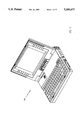
- FIG. 1 illustrates in perspective view a notebook type portable computer system labelled with reference numeral 100.
- System 100 typically has a seven volt main battery made of six 1.2 volt rechargeable nickel-cadmium cells in series and battery power manager for supplying the various power needs, such as 3.3 and 5 volts regulated DC for CMOS devices, 12 volts regulated DC for Flash EEPROM programming, and high voltage AC for the backlightling lamps of the LCD screen.
- the system typically includes various DC to DC regulators (converters) and a DC to AC inverter.
- the 5 volt regulator may have a specification such as: provide a regulated 5 volt output of up to 5 amps from an input in a range such as 7 to 25 volts.
- FIG. 2A schematically shows a known 5 volt regulator.
- the regulator should deliver a steady, regulated DC voltage with a small dropout voltage; that is, the unregulated input voltage need only be slightly larger than the output regulated voltage for proper operation.
- known low voltage regulators only achieve moderate efficiencies for small dropout voltages. Generally, see Pressman, Switching Power Supply Design (McGraw-Hill 1991).
- Prior art regulator 200 of FIG. 2A takes battery 210 as input power at voltage V in and outputs power at regulated voltage V out ; the regulation derives from the feedback of V out to controller 220.
- Regulator 200 operates basically as follows: controller 220 includes an oscillator to drive the gates of n-channel field effect transistors (FETs) 222 and 224 with the output feedback determining the duty cycle of the drive; see the first two panels of FIG. 2B.
- FETs field effect transistors
- Controller 220 sets V out by varying the duty cycle of FETs 222 and 224. Indeed, V out equals V in multiplied by the duty cycle of pass FET 222 if losses are ignored. Inductor 232 and capacitor 234 form a low pass filter for V out , so if the oscillator of controller 220 has a high enough frequency, V out will have essentially no harmonics.
- Known regulators 200 have problems including a lack of efficiency in extracting power from a battery input with a battery voltage not much above the regulated output voltage (a large dropout voltage at high currents). Thus known regulators have required excess battery input voltage (i.e., using six rather than five 1.2 volt cells in series for the standard 5 volt output) or not fully utilizing the battery energy and requiring more frequent replacement than necessary. The use of six rather than five cells increases battery weight which limits portability. Further, if free-wheeling FET 224 turns on before pass FET 222 turns off, or vice versa, a large transient "shoot through" current can flow directly from battery. 210 to ground. Such shoot through can occur when the gate capacitances of the FETs leads to simultaneous turn on.
- the present invention provides a grator with small dropout voltage (0.3 volts at 5 amps) and minimal shoot through current by use of an adaptive synchronous recitifier.
- FIG. 1 perspectively illustrates a laptop computer
- FIGS. 2A-B schematically shows a known regulator and its waveforms
- FIGS. 3A-E are schematic circuit block diagrams of a first preferred embodiment system
- FIG. 4 a schematic circuit diagram of a the first preferred embodiment regulator
- FIG. 5 shows waveforms
- FIG. 6 shows another preferred embodiment.
- FIG. 3A is a schematic block diagram of a first preferred embodiment portable computer system which includes microprocessor 300, bus and memory controller 310, bus 311, memory 312, power consumption management 320, video controller 330, hard disk drive 340, and input/output controller 350.
- FIGS. 3B-E show more detailed portions of FIG. 3A.
- FIG. 3B illustrates memory expansion with optional 1 or 2 megabyte modules 316 and 314 plus DC--DC regulator (converter) 362 that takes as input power from the rechargeable battery at about 6 volts (five 1.2 volt NiCd or NiMH 4 cells) and outputs 12 volts for programming Flash EEPROM 360 which contains the boot program.
- FIG. 3C shows LCD panel 336 and first preferred embodiment inverter 334 which provides the AC power for the backlighting of panel 336.
- FIG. 3D illustrates further aspects of power consumption management controller 320, and FIG.
- 3E shows connections to input/output controller 350 such as keyboard 380, mouse port 386, RS 232 interface 352, optional modem 354, and printer port 390.
- the preferred embodiment DC--DC regulator which outputs 5 volts (actually 4.8 volts may be used) to power all of the CMOS devices such as microprocessor 300, controller 310, and so forth is not explicitly shown in any of FIGS. 3A-E.
- FIG. 4 schematically shows first preferred embodiment DC--DC regulator 400.
- Regulator 400 basically includes an input terminal for unregulated dc input V in (typically supplied by a battery), an output terminal for regulated output V out , n-channel pass FET 422 and n-channel free-wheeling FET 424, inductor 432, diode 436, and capacitor 434.
- regulator 400 includes the following components: low power, low dropout voltage regulator 402 which may be an LM2931; 555-type timer 404 which may be a TLC555; reset generator 406 which may be a TL7705; D flip-flops 408-409 which may each be a half of a 74ACT74; comparators 411-413 which may be portions of a UC3707 with comparator 413 providing blanking of the outputs of comparators 411-412; and discrete transistors, diodes, resistors, capacitors, and switches as shown in FIG. 4.
- low power, low dropout voltage regulator 402 which may be an LM2931
- 555-type timer 404 which may be a TLC555
- reset generator 406 which may be a TL7705
- D flip-flops 408-409 which may each be a half of a 74ACT74
- comparators 411-413 which may be portions of a UC3707 with comparator 413 providing blanking of the outputs of comparators 411-4
- Regulator 400 can provide a V out of +5 volts (standard for CMOS devices) at 5 amps for an input V in between 5.3 volts and 25 volts, thus a battery supply for V in could be just five 1.2 volt recharageable NiCd or NiMH 4 cells.
- NiCd or NiMH 4 cells will vary from 1.25 volts down to close to 1.0 volt when close to 100% discharged, and typical CMOS integrated circuit operation requires a minimum power supply voltage of about 4.8 volts. Thus only five cells are needed if a low dropout voltage can be achieved.
- Regulator 400 also provides power-fail reset (reset generator 406), electronic power switching (DPDT 471), boosted output voltage (voltage doubler diode 451, capacitor 452, diode 453 and capacitor 454) which can control battery ORing circuit, soft start, power supply for a real time clock (low power regulator 402), and a voltage feed-forward control loop. These features combine to make a small and efficient, low cost power subsystem.
- Regulator 400 operates as follows.
- the input unregulated dc supply V in powers low power regulator 402 which outputs a regulated +4.5 volts.
- the regulated +4.5 volts provides an internal power supply Vcc for regulator 400 devices plus power for low power items such as a real time clock.
- Timer 404 has its threshold and trigger inputs (pins 2 and 6) connected to put it into an astable (oscillating) mode with a periodic output (at pin 3) switching between 0 and Vcc.
- the duty cycle of the periodic output approximates 99% and is determined by the RC time constant to charge up (from 1/3 Vcc to 2/3 Vcc) 470 pF capacitor 441 through 22 Kohm resistor 442 when the periodic output is high (duration roughly 10 microseconds) and the discharge time of capacitor 44 1 through diode 443 when the periodic output is low (duration roughly 100 nanoseconds).
- the square wave periodic output of timer 404 has a frequency of roughly 100 KHz, although this can be easily changed by varying the values of resistor 442 or capacitor 441.
- the rising edge of this output square wave is integrated by resistor 445 and capacitor 446 (RC about 300 nanoseconds) and clocks flip-flop 408. This integration delay allows for flip-flop 408 setup time.
- the discharge input (pin 7) of timer 404 is active when the periodic output is low and pulls the reset input of flip-flop 408 low to reset the flip-flop.
- feedback from V out through FET 460 will in fact provide an earlier reset input to flip-flop 408 and shorten the duty cycle of Q as shown by the broken lines in the fourth and fifth panels of FIG. 5.
- the Q and Q# (Q-bar) outputs of flip-flop 408 drive the positive and negative inputs of comparator 411, respectively, and comparator 411, in turn, drives the gate of pass FET 422.
- the output level of comparator 411 derives from power input Vc which connects to voltage-doubling node 450, so the gate of n-channel pass FET 422 is boosted above V in to eliminate the threshold drop. Note that if the V in input were used as the output for comparator 411, then the gate of pass FET 422 would be at most at V in and pass FET 422 would limit the voltage of node 430 to a threshold less than V in and the dropout voltage would increase.
- Voltage-doubling node 450 operates as follows: when pass FET 422 is off and free-wheeling FET 424 is on, then node 430 is slightly above ground and node 450 is a diode drop below V in . Hence, capacitor 452 is charged to about V in minus a diode drop. When free-wheeling FET 424 turns off and pass FET 422 turns on, node 430 jumps up to V in , So capacitor 452 pushes node 450 up to about 2V in minus a diode drop. Hence, when pass FET 422 turns on an extra voltage boost occurs to insure the gate voltage is well above V in . Note that the peak voltage at node 450 turns on diode 453 and stores on capacitor 454 to provide a roughly 2V in supply.
- the Q# output of flip-flop 408 also drives the positive input of comparator 412, and the negative input connects through diode 415 to the gate of pass FET 422.
- the voltage on the gate of pass FET 422 must first drop below Q# minus a diode drop and be turning off pass FET 422 before comparator 412 starts to switch high to turn on free-wheeling FET 424. This contrasts with the case of Q# and Q alone driving comparator 412.
- the slow turn on of FET 424 helps prevent shoot-through current from V in to ground which would occur if FETs 422 and 424 are both on simultaneuosly.
- diode 436 provides the loop current path when FETs 422 and 424 are simultaneously off.
- blanking comparator 413 blanks the outputs of comparators 411 and 412 when the periodic output of timer 404 is low, as follows.
- the control output (pin 5) of timer 404 provides a constant 2/3 Vcc to the positive input of comparator 413 and the periodic output of timer 404 provides the negative input of comparator 413, so comparator 413 outputs short (100 nanosecond) high pulses at 100 KHz corresponding to lows in the periodic output.
- These pulses blank the outputs of comparators 411 and 412 by internal connections not shown in FIG. 4. This blanking insures that pass FET 422 and free-wheeling FET 424 will not be on at the same time when pass FET 422 is turning off and an earlier reset through FET 460 (see following discussion) has not occurred.
- Regulator 463 will thus turn on to conduct when V out reaches 5 volts.
- the emitter and base of pnp 468 will both be at V out and pnp 468 will be off until regulator 463 conducts and generates a emitter base bias.
- regulator 463 conducts and turns on pnp 468 to charge up capacitor 461 if Q is high; otherwise the current from pnp 468 is shunted to ground by diode 462 if Q is low.
- V out at least +5 volts
- pnp 468 begins charging up capacitor when Q switches from low to high 300 nanoseconds after the periodic output of timer 404 switches from low to high.
- regulator 463, pnp 468, and the resistors form a voltage to current converter, and the output current charges capacitor 461.
- the charging rate of capacitor 461 determines the duty cycle of Q and pass FET 422.
- V out equals V in multiplied by the duty cycle of the pass FET, so the feedback stabilizes V out at the level determined by shunt regulator 463.
- the voltage drop of pass FET 422 when driven by the voltage doubler is only about 0.1-0.2 volt even for a 5 amp current, and because timer 404 provides an output with a 99% duty cycle, V out will be maintained at +5 volts even when V in drops to 5.3 volts. That is, the dropout voltage is 0.3 volt.
- the duty cycle of FET 422 must be small (below 20% for 27 volts at V in ) and thus the current from pnp 468 charging capacitor must be larger because most of it is shunted to ground by diode 462 when Q is low.
- up to 2V in appears at the gate of FET 422, whereas the source is only at V out , so up to 2V in -V out appears across the gate oxide.
- Zener diode 490 provides an output crowbar to protect the load at V out in case pass FET 422 fails; the Zener voltage is 6.2 volts.
- Flip-flop 409 provides a combination fault latch, low battery shutdown, and an electronic power switch.
- double pole double throw (DPDT) switch 471 controls the electronic switch as follows.
- DPDT 471 in the off position implies both the set and reset inputs of flip-flop 409 are low and the control (pin 5) of timer 404 is held low.
- set and reset inputs of flip-flop 409 both low drives both Q and Q# high; and Q high (Vcc) turns off FET 473 whose gate is also at Vcc.
- no current flow means resistor 474 does not develop a voltage drop and FET 475 turns off to cut off V in power to comparators 411-413 and thus disable pass FET 422 and free-wheeling FET 424.
- diode 477 holds the reset input (pin 4) of timer 404 low despite Q# of flip-flop 409 being high, and reset low interrupts the oscillation and puts timer 404 in the nontriggered state.
- DPDT 471 in the off position turns off V out and limits regulator 400 to a very low power consumption: about 100 microamps.
- DPDT 471 switched into the on position forces the set and reset and data inputs of flip-flop 409 high, but the RC time constant of resistor 481 and capacitor 482 delays the reset high.
- Q originally goes low, and this turns on FETs 473 and 474 to apply V in to comparators 411-413 and thereby turn on pass FET 422 to start V out rising.
- capacitor 444 charges up through the internal resistor of timer 404 to its 2/3 Vcc level, and during this ramp up of the capacitor 444 voltage the internal comparator reference points are lower.
- timer 404 will oscillate at a higher frequency due to the smaller voltage swing on capacitor 441 firing the trigger and threshold comparators.
- Timer 404 thus will clock flip-flop 408 at a faster rate, but the RC delay by resistor 445 and capacitor 446 does not change, so the duty cycle of Q decreases and a "soft start” powering up of V out occurs rather than a sudden jump in voltage. Indeed, the oscillation period of timer 404 varies roughly linearly with the charge on capacitor 444.
- Reset generator 406 provides a reset pulse (RESET#) upon V out being out of tolerance.
- the reset pulse resets the microprocessor such as CPU 102 in FIG. 1 when power returns to an in-tolerance condiction after being in an out-of-tolerance condiction.
- Reset generator 406 contains an internal reference voltage (bandgap generator) with which it compares the power supply voltage V out .
- V in minimally greater than V out
- Q from flip-flop 408 and pass FET 422 will have a maximum duty cycle (99%) and the blanking by comparator 413 will effectively keep free-wheeling FET 424 always off.
- voltage doubler capacitor 452 will not charge and will fail to boost the gate voltage of pass FET 422 which will not saturate.
- the reset pulse from reset generator 406 suppresses the blanking by comparator 413 through diode 488.
- free-wheeling FET 424 will turn on for a time period determined by the propagation delay of comparator 412.
- Such blanking suppression permits doubler capacitor 452 to charge up but also allows shoot-through current due to the overlapping conductivity of pass FET 422 and free-wheeling FET 424.
- doubler capacitor 452 typically takes less than 500 milliseconds to charge up, and the shoot-through current during the overlaps of FET 422 and FET 424 conductivity for such a short interval can be tolerated.
- the dropout voltage depends upon the voltage drop in saturated pass FET 422 plus the voltage drop in inductor 432.
- the voltage drop in pass FET 422 will be small due to the boosted gate voltage, and the voltage drop in inductor 432 depends upon the current and the resistance of the windings. Now the resistance of the windings is proportinoal to the inductance, and a lower inductance can be used with a higher frequency of oscillation by timer 404. But as oscillation frequency increases, switching losses increase. Also, as the average current drops, intervals of zero current in inductor 432 will occur and make the necessary duty cycle depend upon output current, so a minimum current is needed to avoid a output current dependence.
- regulator 400 is to fit on a circuit board within a portable computer, so the overall physical size has limits, and thus inductor 432 cannot be made of arbitrarily heavy wire.
- the inductor resistance dominates the approximate 10 milliohm on-resistance of pass FET 422 and determines the dropout voltage.
- FIG. 5 illustrates the voltage waveforms observed in inverter 300.
- the first panel shows the voltage ramp on trigger capacitor 441 of timer 404; the ramp rate depends upon the resistor 442 and capacitor 441 values.
- the second panel shows the periodic output of timer 404 at pin 3; this amounts to a series of low spikes.
- the third panel indicates the CLK input of flip-flop 408 which is the pin 3 output of timer 404 after passing the integrator made of resistor 445 and capacitor 446; the duration of the low has been exaggerated for clarity.
- the Q output flip-flop 408 appears in the fourth panel with the pass FET 422 duty cycle variation due to earlier resets of flip-flop 408 by feedback driving FET 460 indicated by the broken line.
- the last panel shows the variation in charging rate of capacitor 461 that comes from the feedback and determines the driving of FET 460 and the duty cycle.
- the preferred embodiments may be modified in many ways while retaining one of more of the features of an adaptive synchronous rectifier.
- FIG. 6 shows a variant regulator in combination with other power supply circuits.
- the righthand portion of FIG. 6 shows a regulator 600 similar to regulator 400 but with low power regulator 602 explicitly shown (this regulator employs the pnp 603 with feedback for regulation).
- regulator 600 has two pass FETs 622-623 in parallel to lessen the dropout voltage.
- the lefthand portion of FIG. 6 shows +12 volt regulator 692 and -11 to -22 volt inverting regulator 694.
- Regulator 692 has timer 693 directly switching its pass FET, and regulator 694 has timer 695 directly switching its pass FET; and timers 693 and 695 are synchronized to timer 604 by the output (pin 3) of timer 604 driving the trigger inputs of timers 693 and 695. This synchrony limits the noise spectrum of the regulator combination.
- the feedback duty cycle control of regulators 692 and 694 relies on sampling the output voltages and coupling the sampled voltages to the control input (pin 5) of the corresponding timer.
Abstract
Description
Claims (22)
Priority Applications (1)
| Application Number | Priority Date | Filing Date | Title |
|---|---|---|---|
| US07/874,143 US5355077A (en) | 1992-04-27 | 1992-04-27 | High efficiency regulator with shoot-through current limiting |
Applications Claiming Priority (1)
| Application Number | Priority Date | Filing Date | Title |
|---|---|---|---|
| US07/874,143 US5355077A (en) | 1992-04-27 | 1992-04-27 | High efficiency regulator with shoot-through current limiting |
Publications (1)
| Publication Number | Publication Date |
|---|---|
| US5355077A true US5355077A (en) | 1994-10-11 |
Family
ID=25363074
Family Applications (1)
| Application Number | Title | Priority Date | Filing Date |
|---|---|---|---|
| US07/874,143 Expired - Lifetime US5355077A (en) | 1992-04-27 | 1992-04-27 | High efficiency regulator with shoot-through current limiting |
Country Status (1)
| Country | Link |
|---|---|
| US (1) | US5355077A (en) |
Cited By (32)
| Publication number | Priority date | Publication date | Assignee | Title |
|---|---|---|---|---|
| US5608314A (en) * | 1994-04-11 | 1997-03-04 | Advanced Micro Devices, Inc. | Incremental output current generation circuit |
| US5691889A (en) * | 1995-12-13 | 1997-11-25 | Unitrode Corporation | Controller having feed-forward and synchronization features |
| US5721485A (en) * | 1996-01-04 | 1998-02-24 | Ibm Corporation | High performance on-chip voltage regulator designs |
| US5774734A (en) * | 1994-10-07 | 1998-06-30 | Elonex I.P. Holdings, Ltd. | Variable-voltage CPU voltage regulator |
| US5814979A (en) * | 1995-06-01 | 1998-09-29 | Maxim Integrated Products, Inc. | Low drop out switching regulator |
| US5864457A (en) * | 1997-01-21 | 1999-01-26 | Dell Usa, L.P. | System and method for controlling current flow in an AC adapter |
| US5912552A (en) | 1997-02-12 | 1999-06-15 | Kabushiki Kaisha Toyoda Jidoshokki Seisakusho | DC to DC converter with high efficiency for light loads |
| US5916313A (en) * | 1996-10-31 | 1999-06-29 | Dell U. S. A., L.P. | Low cost power converter for a computer |
| US5939871A (en) | 1996-02-01 | 1999-08-17 | Kabushiki Kaisha Toyoda Jidoshokki Seisakusho | DC/DC converter and controller therefor utilizing an output inductor current and input voltage |
| US6058034A (en) * | 1998-10-19 | 2000-05-02 | Dell Usa Lp | Current converter and source identification and detection |
| US6130528A (en) | 1997-05-09 | 2000-10-10 | Kabushiki Kaisha Toyoda Jidoshokki Seisakusho | Switching regulator controlling system having a light load mode of operation based on a voltage feedback signal |
| US6130813A (en) * | 1999-01-11 | 2000-10-10 | Dell U.S.A., L.P. | Protection circuit for electronic devices |
| US6137280A (en) * | 1999-01-22 | 2000-10-24 | Science Applications International Corporation | Universal power manager with variable buck/boost converter |
| US6191552B1 (en) | 1999-01-25 | 2001-02-20 | Dell Usa, L.P. | External universal battery charging apparatus and method |
| US6204650B1 (en) * | 1998-03-20 | 2001-03-20 | Fujitsu, Limited | Power supply apparatus and method of controlling power supply circuit for generating a DC output |
| FR2802315A1 (en) * | 1999-12-13 | 2001-06-15 | St Microelectronics Sa | VOLTAGE REGULATOR WITH BALLAST TRANSISTOR AND CURRENT LIMITER |
| EP1132802A1 (en) * | 2000-02-17 | 2001-09-12 | Robert Bosch Gmbh | Supply voltage booster for electronic assemblies |
| FR2807846A1 (en) * | 2000-04-12 | 2001-10-19 | St Microelectronics Sa | LOW POWER CONSUMPTION VOLTAGE REGULATOR |
| US6396333B2 (en) * | 2000-01-04 | 2002-05-28 | International Rectifier Corporation | Circuit for synchronous rectification with minimal reverse recovery losses |
| US20020196004A1 (en) * | 2001-05-22 | 2002-12-26 | Yuval Berson | Power distribution with digital current control |
| US6577515B2 (en) | 2001-03-02 | 2003-06-10 | Advanced Micro Devices, Inc. | Asymmetric power supply including a fast response converter |
| US20030191596A1 (en) * | 1998-09-16 | 2003-10-09 | Microchip Technology Incorporated | Programmable power supply and brownout detector for electronic equipment |
| US6661208B2 (en) * | 2001-02-06 | 2003-12-09 | Koninklijke Philips Electronics N.V. | Synchronous DC-DC regulator with shoot-through prevention |
| US6687142B2 (en) | 2001-12-17 | 2004-02-03 | Coolit Systems Inc. | AC to DC inverter for use with AC synchronous motors |
| US6693782B1 (en) | 2000-09-20 | 2004-02-17 | Dell Products L.P. | Surge suppression for current limiting circuits |
| US20090167091A1 (en) * | 2003-02-11 | 2009-07-02 | O2Micro International Limited | Selector circuit for power management in multiple battery systems |
| US20090278499A1 (en) * | 2000-09-21 | 2009-11-12 | O2Micro, Inc. | Method and electronic circuit for efficient battery wake up charging |
| US20100327813A1 (en) * | 2000-09-21 | 2010-12-30 | O2Micro International Limited | Power management topologies |
| US20130313995A1 (en) * | 2012-05-25 | 2013-11-28 | Laurence P. Sadwick | Dimmable LED Driver |
| US9760520B2 (en) | 2014-07-11 | 2017-09-12 | Covidien Lp | Dynamic system management bus for an electrosurgical system |
| US10199950B1 (en) | 2013-07-02 | 2019-02-05 | Vlt, Inc. | Power distribution architecture with series-connected bus converter |
| US20210063988A1 (en) * | 2019-08-26 | 2021-03-04 | Rockwell Automation Asia Pacific Business Centre Pte. Ltd. | High Current and Power Limiting Circuit for I/O Modules with Internal Output Power Support |
Citations (13)
| Publication number | Priority date | Publication date | Assignee | Title |
|---|---|---|---|---|
| US4161023A (en) * | 1977-09-07 | 1979-07-10 | The United States Of America As Represented By The United States Department Of Energy | Up-and-down chopper circuit |
| US4538101A (en) * | 1982-06-04 | 1985-08-27 | Nippon Chemi-Con Corporation | Power supply device |
| US4672303A (en) * | 1986-08-28 | 1987-06-09 | International Business Machines Corporation | Inductor current control circuit |
| US4801859A (en) * | 1986-12-23 | 1989-01-31 | Sundstrand Corporation | Boost/buck DC/DC converter |
| US4825144A (en) * | 1987-11-10 | 1989-04-25 | Motorola, Inc. | Dual channel current mode switching regulator |
| US4931716A (en) * | 1989-05-05 | 1990-06-05 | Milan Jovanovic | Constant frequency zero-voltage-switching multi-resonant converter |
| US5066900A (en) * | 1989-11-14 | 1991-11-19 | Computer Products, Inc. | Dc/dc converter switching at zero voltage |
| US5072171A (en) * | 1990-01-23 | 1991-12-10 | Hughes Aircraft Company | High efficiency power converter employing a synchronized switching system |
| US5097196A (en) * | 1991-05-24 | 1992-03-17 | Rockwell International Corporation | Zero-voltage-switched multiresonant DC to DC converter |
| US5128603A (en) * | 1989-05-05 | 1992-07-07 | Alcatel N.V. | Forward converter using an inverter including a transistor |
| US5130561A (en) * | 1990-08-29 | 1992-07-14 | Alcatel Network Systems, Inc. | Switching mode power supplies with controlled synchronization |
| US5138249A (en) * | 1990-06-08 | 1992-08-11 | Alcatel Espace | Circuit for regulating a parameter by means of a bidirectional current structure |
| US5142217A (en) * | 1991-03-07 | 1992-08-25 | Sgs-Thomson Microelectronics, Inc. | Synchronizable power supply controller and a system incorporating the same |
-
1992
- 1992-04-27 US US07/874,143 patent/US5355077A/en not_active Expired - Lifetime
Patent Citations (13)
| Publication number | Priority date | Publication date | Assignee | Title |
|---|---|---|---|---|
| US4161023A (en) * | 1977-09-07 | 1979-07-10 | The United States Of America As Represented By The United States Department Of Energy | Up-and-down chopper circuit |
| US4538101A (en) * | 1982-06-04 | 1985-08-27 | Nippon Chemi-Con Corporation | Power supply device |
| US4672303A (en) * | 1986-08-28 | 1987-06-09 | International Business Machines Corporation | Inductor current control circuit |
| US4801859A (en) * | 1986-12-23 | 1989-01-31 | Sundstrand Corporation | Boost/buck DC/DC converter |
| US4825144A (en) * | 1987-11-10 | 1989-04-25 | Motorola, Inc. | Dual channel current mode switching regulator |
| US5128603A (en) * | 1989-05-05 | 1992-07-07 | Alcatel N.V. | Forward converter using an inverter including a transistor |
| US4931716A (en) * | 1989-05-05 | 1990-06-05 | Milan Jovanovic | Constant frequency zero-voltage-switching multi-resonant converter |
| US5066900A (en) * | 1989-11-14 | 1991-11-19 | Computer Products, Inc. | Dc/dc converter switching at zero voltage |
| US5072171A (en) * | 1990-01-23 | 1991-12-10 | Hughes Aircraft Company | High efficiency power converter employing a synchronized switching system |
| US5138249A (en) * | 1990-06-08 | 1992-08-11 | Alcatel Espace | Circuit for regulating a parameter by means of a bidirectional current structure |
| US5130561A (en) * | 1990-08-29 | 1992-07-14 | Alcatel Network Systems, Inc. | Switching mode power supplies with controlled synchronization |
| US5142217A (en) * | 1991-03-07 | 1992-08-25 | Sgs-Thomson Microelectronics, Inc. | Synchronizable power supply controller and a system incorporating the same |
| US5097196A (en) * | 1991-05-24 | 1992-03-17 | Rockwell International Corporation | Zero-voltage-switched multiresonant DC to DC converter |
Cited By (52)
| Publication number | Priority date | Publication date | Assignee | Title |
|---|---|---|---|---|
| US5608314A (en) * | 1994-04-11 | 1997-03-04 | Advanced Micro Devices, Inc. | Incremental output current generation circuit |
| US5774734A (en) * | 1994-10-07 | 1998-06-30 | Elonex I.P. Holdings, Ltd. | Variable-voltage CPU voltage regulator |
| US5955872A (en) * | 1995-06-01 | 1999-09-21 | Maxim Integrated Products, Inc. | Low drop-out switching regulators |
| US5814979A (en) * | 1995-06-01 | 1998-09-29 | Maxim Integrated Products, Inc. | Low drop out switching regulator |
| US5691889A (en) * | 1995-12-13 | 1997-11-25 | Unitrode Corporation | Controller having feed-forward and synchronization features |
| US5721485A (en) * | 1996-01-04 | 1998-02-24 | Ibm Corporation | High performance on-chip voltage regulator designs |
| US5939871A (en) | 1996-02-01 | 1999-08-17 | Kabushiki Kaisha Toyoda Jidoshokki Seisakusho | DC/DC converter and controller therefor utilizing an output inductor current and input voltage |
| US5916313A (en) * | 1996-10-31 | 1999-06-29 | Dell U. S. A., L.P. | Low cost power converter for a computer |
| US5864457A (en) * | 1997-01-21 | 1999-01-26 | Dell Usa, L.P. | System and method for controlling current flow in an AC adapter |
| US5912552A (en) | 1997-02-12 | 1999-06-15 | Kabushiki Kaisha Toyoda Jidoshokki Seisakusho | DC to DC converter with high efficiency for light loads |
| US6130528A (en) | 1997-05-09 | 2000-10-10 | Kabushiki Kaisha Toyoda Jidoshokki Seisakusho | Switching regulator controlling system having a light load mode of operation based on a voltage feedback signal |
| US6204650B1 (en) * | 1998-03-20 | 2001-03-20 | Fujitsu, Limited | Power supply apparatus and method of controlling power supply circuit for generating a DC output |
| US20030191596A1 (en) * | 1998-09-16 | 2003-10-09 | Microchip Technology Incorporated | Programmable power supply and brownout detector for electronic equipment |
| US7225088B2 (en) * | 1998-09-16 | 2007-05-29 | Microchip Technology Incorporated | Programmable power supply and brownout detector for electronic equipment |
| US6058034A (en) * | 1998-10-19 | 2000-05-02 | Dell Usa Lp | Current converter and source identification and detection |
| US6130813A (en) * | 1999-01-11 | 2000-10-10 | Dell U.S.A., L.P. | Protection circuit for electronic devices |
| US6137280A (en) * | 1999-01-22 | 2000-10-24 | Science Applications International Corporation | Universal power manager with variable buck/boost converter |
| US6191552B1 (en) | 1999-01-25 | 2001-02-20 | Dell Usa, L.P. | External universal battery charging apparatus and method |
| US6337557B1 (en) | 1999-01-25 | 2002-01-08 | Barry K. Kates | External universal battery charging apparatus and method |
| FR2802315A1 (en) * | 1999-12-13 | 2001-06-15 | St Microelectronics Sa | VOLTAGE REGULATOR WITH BALLAST TRANSISTOR AND CURRENT LIMITER |
| EP1109088A1 (en) * | 1999-12-13 | 2001-06-20 | STMicroelectronics SA | Voltage regulator with ballast-transistor and current limiting |
| US6346799B2 (en) | 1999-12-13 | 2002-02-12 | Stmicroelectronics S.A. | Voltage regulator with a ballast transistor and current limiter |
| US6396333B2 (en) * | 2000-01-04 | 2002-05-28 | International Rectifier Corporation | Circuit for synchronous rectification with minimal reverse recovery losses |
| EP1132802A1 (en) * | 2000-02-17 | 2001-09-12 | Robert Bosch Gmbh | Supply voltage booster for electronic assemblies |
| US6501253B2 (en) | 2000-04-12 | 2002-12-31 | Stmicroelectronics S.A. | Low electrical consumption voltage regulator |
| FR2807846A1 (en) * | 2000-04-12 | 2001-10-19 | St Microelectronics Sa | LOW POWER CONSUMPTION VOLTAGE REGULATOR |
| EP1148404A1 (en) * | 2000-04-12 | 2001-10-24 | STMicroelectronics SA | Voltage regulator with low power consumption |
| US6693782B1 (en) | 2000-09-20 | 2004-02-17 | Dell Products L.P. | Surge suppression for current limiting circuits |
| US20090278499A1 (en) * | 2000-09-21 | 2009-11-12 | O2Micro, Inc. | Method and electronic circuit for efficient battery wake up charging |
| US8350534B2 (en) | 2000-09-21 | 2013-01-08 | O2Micro International, Ltd. | Method and electronic circuit for efficient battery wake up charging |
| US8120312B2 (en) | 2000-09-21 | 2012-02-21 | 02Micro International Limited | Power management topologies to control power between a DC power source and one or more batteries to a system load |
| US20100327813A1 (en) * | 2000-09-21 | 2010-12-30 | O2Micro International Limited | Power management topologies |
| US6661208B2 (en) * | 2001-02-06 | 2003-12-09 | Koninklijke Philips Electronics N.V. | Synchronous DC-DC regulator with shoot-through prevention |
| US6577515B2 (en) | 2001-03-02 | 2003-06-10 | Advanced Micro Devices, Inc. | Asymmetric power supply including a fast response converter |
| US20020196004A1 (en) * | 2001-05-22 | 2002-12-26 | Yuval Berson | Power distribution with digital current control |
| US6650554B2 (en) | 2001-05-22 | 2003-11-18 | Powersine Ltd. | Power factor corrector with efficient ripple attenuator |
| US6841979B2 (en) | 2001-05-22 | 2005-01-11 | Powerdsine, Ltd. | Power distribution with digital current control |
| US6850097B2 (en) | 2001-12-17 | 2005-02-01 | Coolit Systems Inc. | Inverter |
| US20040120170A1 (en) * | 2001-12-17 | 2004-06-24 | Coolit Systems Inc. | Inverter |
| US6687142B2 (en) | 2001-12-17 | 2004-02-03 | Coolit Systems Inc. | AC to DC inverter for use with AC synchronous motors |
| US7804273B2 (en) * | 2003-02-11 | 2010-09-28 | O2Micro International Limited | Selector circuit for power management in multiple battery systems |
| US20090167091A1 (en) * | 2003-02-11 | 2009-07-02 | O2Micro International Limited | Selector circuit for power management in multiple battery systems |
| US20130313995A1 (en) * | 2012-05-25 | 2013-11-28 | Laurence P. Sadwick | Dimmable LED Driver |
| US10199950B1 (en) | 2013-07-02 | 2019-02-05 | Vlt, Inc. | Power distribution architecture with series-connected bus converter |
| US10594223B1 (en) | 2013-07-02 | 2020-03-17 | Vlt, Inc. | Power distribution architecture with series-connected bus converter |
| US11075583B1 (en) | 2013-07-02 | 2021-07-27 | Vicor Corporation | Power distribution architecture with series-connected bus converter |
| US11705820B2 (en) | 2013-07-02 | 2023-07-18 | Vicor Corporation | Power distribution architecture with series-connected bus converter |
| US9760520B2 (en) | 2014-07-11 | 2017-09-12 | Covidien Lp | Dynamic system management bus for an electrosurgical system |
| US10459867B2 (en) | 2014-07-11 | 2019-10-29 | Covidien Lp | Method for dynamic bus communication for an electrosurgical generator |
| US10891249B2 (en) | 2014-07-11 | 2021-01-12 | Covidien Lp | Dynamic system management bus |
| US20210063988A1 (en) * | 2019-08-26 | 2021-03-04 | Rockwell Automation Asia Pacific Business Centre Pte. Ltd. | High Current and Power Limiting Circuit for I/O Modules with Internal Output Power Support |
| US11507042B2 (en) * | 2019-08-26 | 2022-11-22 | Rockwell Automation Asia Pacific Business Centre Pte. Ltd. | High current and power limiting circuit for I/O modules with internal output power support |
Similar Documents
| Publication | Publication Date | Title |
|---|---|---|
| US5355077A (en) | High efficiency regulator with shoot-through current limiting | |
| US5430641A (en) | Synchronously switching inverter and regulator | |
| EP0721691B1 (en) | System and method for dual mode dc-dc power conversion | |
| US5999429A (en) | Bulk filter capacitor discharge in a switching power supply | |
| CN102217179B (en) | Dc-dc converter | |
| EP1820077B1 (en) | High efficiency dc-to-dc synchronous buck converter | |
| Namgoong et al. | A high-efficiency variable-voltage CMOS dynamic dc-dc switching regulator | |
| US5657257A (en) | Power-supply controller of computer | |
| EP0617501B2 (en) | Control circuit for maintaining high efficiency over broad current ranges in a switching regulator circuit | |
| CN1812235B (en) | Electronic component for power supply and a power supply device | |
| US6414403B2 (en) | Power unit | |
| US6480401B2 (en) | Method and apparatus for reducing standby power in power supplies | |
| US20050099164A1 (en) | Pfc-pwm controller having interleaved switching | |
| US20090153127A1 (en) | Method and apparatus for external control mode step down switching regulator | |
| US20090072626A1 (en) | Power supply apparatus having switchable switching regulator and linear regulator | |
| US5808881A (en) | Power-supply controller of computer | |
| US6198262B1 (en) | Selective dual input low dropout linear regulator | |
| WO2010002906A2 (en) | Voltage converters | |
| TW571496B (en) | Power supply apparatus | |
| US6577110B2 (en) | DC-to-DC converter with constant ripple current regulation for continuous and discontinuous conduction mode operation | |
| US8810212B2 (en) | Microcomputer and switching power supply device with auxiliary switch | |
| US7212418B1 (en) | Synchronous rectifier control circuit | |
| WO2004047249A3 (en) | Control ic for low power auxiliary supplies | |
| US7492131B2 (en) | Variable drive switching regulator architecture | |
| JP3566056B2 (en) | Electronics |
Legal Events
| Date | Code | Title | Description |
|---|---|---|---|
| AS | Assignment |
Owner name: DELL USA L.P., A CORP. OF DE, TEXAS Free format text: ASSIGNMENT OF ASSIGNORS INTEREST.;ASSIGNOR:KATES, BARRY K.;REEL/FRAME:006105/0047 Effective date: 19920415 Owner name: DELL USA L.P., A TEXAS LIMITED PARTNERSHIP, TEXAS Free format text: ASSIGNMENT OF ASSIGNORS INTEREST.;ASSIGNOR:KATES, BARRY K.;REEL/FRAME:006105/0049 Effective date: 19920415 |
|
| STCF | Information on status: patent grant |
Free format text: PATENTED CASE |
|
| FPAY | Fee payment |
Year of fee payment: 4 |
|
| FPAY | Fee payment |
Year of fee payment: 8 |
|
| REMI | Maintenance fee reminder mailed | ||
| FEPP | Fee payment procedure |
Free format text: PAYOR NUMBER ASSIGNED (ORIGINAL EVENT CODE: ASPN); ENTITY STATUS OF PATENT OWNER: LARGE ENTITY |
|
| FPAY | Fee payment |
Year of fee payment: 12 |