US5394655A - Semiconductor polishing pad - Google Patents
Semiconductor polishing pad Download PDFInfo
- Publication number
- US5394655A US5394655A US08/114,532 US11453293A US5394655A US 5394655 A US5394655 A US 5394655A US 11453293 A US11453293 A US 11453293A US 5394655 A US5394655 A US 5394655A
- Authority
- US
- United States
- Prior art keywords
- polishing
- grooves
- wafer
- pad
- circumferential edge
- Prior art date
- Legal status (The legal status is an assumption and is not a legal conclusion. Google has not performed a legal analysis and makes no representation as to the accuracy of the status listed.)
- Expired - Lifetime
Links
Images

Classifications
-
- B—PERFORMING OPERATIONS; TRANSPORTING
- B24—GRINDING; POLISHING
- B24B—MACHINES, DEVICES, OR PROCESSES FOR GRINDING OR POLISHING; DRESSING OR CONDITIONING OF ABRADING SURFACES; FEEDING OF GRINDING, POLISHING, OR LAPPING AGENTS
- B24B37/00—Lapping machines or devices; Accessories
- B24B37/11—Lapping tools
- B24B37/20—Lapping pads for working plane surfaces
- B24B37/26—Lapping pads for working plane surfaces characterised by the shape of the lapping pad surface, e.g. grooved
Definitions
- This invention relates to semiconductor materials, and more particularly to a polishing pad and method for polishing semiconductor wafers.
- polishing provides a smooth surface and removes irregularities that interfere with the various diffusion and masking processes utilized in making uniform devices across the surface of the wafer. Polishing is accomplished by mounting several semiconductor wafers in openings in a wafer holder and putting the wafers and holder between two polishing plates that have polishing pads thereon. The wafer holder is rotated and rolled around the periphery of the polishing machine to provide a planetary motion of the wafers during polishing. The movement of the wafer against the polishing pad is used in conjunction with an abrasive slurry of a fine particle size to provide the desired smoothness.
- nonflat polishing occurs at the edge of the wafer, with the wafer edge receiving more polishing than the central portions, resulting in a "pillow-shaped" wafer. This provides an undesired tapering of the wafer from the center to the edges.
- the invention provides an improved polishing pad and its method of use.
- the polishing pad has portions of the polishing surface removed by reducing the pad thickness, so that the parts of a wafer surface passing over the reduced thickness non-polishing portions of the pad are not polished as much as other parts of the wafer surface.
- the paths of the wafer surface contacting the polishing pad are predictable, therefore it is known which part of the wafer surface will receive minimum polishing.
- the parts of the pad surface removed are predetermined so that the polishing will not cause tapering of the wafer edges.
- an annular circular pad has two strips of the pad polishing surface removed by locally reducing the thickness of the pad, one strip adjacent the outer circumferential edge of the pad, and another strip adjacent the inner circumferential edge of the polishing pad.
- the motion of the wafers around the pad, and the rotation of the wafers in the wafer holder puts the edges of the wafers over the reduced portions of the pad more than the central portions of the wafers, are put over the same portion. This removes less surface of the outer edges of the wafer, thereby avoiding the non-flatness which occurs when the wafers are polished with pads not having the rings of the pad polishing surface removed.
- the reduced portions may be continuous rings, or segmented rings which add more strength to the polish pad than the continuous ring configuration. Edges of the removed strips are tapered to prevent tearing or binding on teeth of the wafer holder.
- FIG. 1 shows the tapered wear on a semiconductor wafer
- FIG. 2 shows one embodiment of a polishing pad of the present invention
- FIG. 3 is a top view of a wafer polisher with the top backing plate and top polishing pad removed;
- FIG. 4 is a cross-sectional view of a part of a wafer polisher when polishing.
- FIG. 1 illustrates a semiconductor wafer 10 showing uneven wear or tapering at peripheral edge 12. If perfect polishing were accomplished, the surface of the wafer would be essentially flat to the edge as shown at 11.
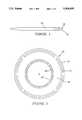
- FIG. 2 shows an embodiment of the polishing pad according to the present invention.
- a flat planar pad 14, having a flat planar polishing surface 19 is in the form of an annular ring, having an outer circumferential edge 15 and an inner circumferential edge 16.
- the thickness of pad 14 is locally reduced to provide two rings 17 and 18 of removed polishing pad 14 surface on a central region of pad intermediate edges 15 and 16.
- the thickness reductions define non-polishing arcuate grooves or channels in the central region, arranged marginally of edges 15 and 16.
- non-polishing rings 17 and 18 are segmented to provide strength to the polishing pad.
- the use of a polishing pad of increased thickness would permit continuous non-polishing rings.
- FIG. 3 illustrates a top view of a polishing pad 14 in place in a partial view of a polishing machine.
- Pad 14 is on a polishing plate 26 (FIG. 4).
- a wafer holder 20 which, as illustrated, holds four wafers in openings 24.
- Wafer holder 20 has an outer circumference made up of external gear teeth 21. Gear teeth 21 are intermeshed with gear pins 22 and 23 on the polishing machine.
- the backing plate 25 and polishing pad 14 may rotate clockwise or counter clockwise as shown by arrow A.
- the rings of pins 22 and 23 rotate at different rotational velocities.
- FIG. 4 shows a cross-sectional view of part of the polishing equipment.
- Wafer holder 20 is between lower polishing plate 26 and polish pad 14a and upper polish plate 25 and upper polish pad 14.
- Two wafers 20 are shown.
- Non-polishing strip 18 is shown with tapered edges 18a and non-polish strips 17 has tapered edges 17a. The purpose of the taper at the edge of the polish/non-polish interface is to prevent edges that might tear or bind between the teeth of wafer holder 20 and pad 14.
- non-polishing areas are not necessarily circular segments, but may be any shape that will provide predictable selective polishing of the wafer surface.
- polishing pad of the present invention has been made using an apparatus for polishing two sides of a semiconductor wafer, but a single side polishing machine may also provide the desired polishing using the polishing pad.
Landscapes
- Engineering & Computer Science (AREA)
- Mechanical Engineering (AREA)
- Finish Polishing, Edge Sharpening, And Grinding By Specific Grinding Devices (AREA)
- Mechanical Treatment Of Semiconductor (AREA)
Abstract
The invention is to a polishing pad 14 that has a polishing surface 19 in which portions 17 and 18 of the polishing surface 19 have been removed. The removed areas 17 and 18 are annular rings adjacent an outer 15 and inner 16 edges of the polishing pad 14. The non-polishing surfaces 18 and 19 taper 17a and 18a downward from the polishing surface 19.
Description
This invention relates to semiconductor materials, and more particularly to a polishing pad and method for polishing semiconductor wafers.
The surfaces of wafers are polished to prepare them for the various processes during which devices are formed in the surface of the wafer. Polishing provides a smooth surface and removes irregularities that interfere with the various diffusion and masking processes utilized in making uniform devices across the surface of the wafer. Polishing is accomplished by mounting several semiconductor wafers in openings in a wafer holder and putting the wafers and holder between two polishing plates that have polishing pads thereon. The wafer holder is rotated and rolled around the periphery of the polishing machine to provide a planetary motion of the wafers during polishing. The movement of the wafer against the polishing pad is used in conjunction with an abrasive slurry of a fine particle size to provide the desired smoothness. One problem encountered with this process is that, although various controllable factors affecting polishing may be controlled, nonflat polishing occurs. Particularly, non-flatness occurs at the edge of the wafer, with the wafer edge receiving more polishing than the central portions, resulting in a "pillow-shaped" wafer. This provides an undesired tapering of the wafer from the center to the edges.
The invention provides an improved polishing pad and its method of use. The polishing pad has portions of the polishing surface removed by reducing the pad thickness, so that the parts of a wafer surface passing over the reduced thickness non-polishing portions of the pad are not polished as much as other parts of the wafer surface. The paths of the wafer surface contacting the polishing pad are predictable, therefore it is known which part of the wafer surface will receive minimum polishing. The parts of the pad surface removed are predetermined so that the polishing will not cause tapering of the wafer edges.
In an embodiment of the invention described below, an annular circular pad has two strips of the pad polishing surface removed by locally reducing the thickness of the pad, one strip adjacent the outer circumferential edge of the pad, and another strip adjacent the inner circumferential edge of the polishing pad. The motion of the wafers around the pad, and the rotation of the wafers in the wafer holder puts the edges of the wafers over the reduced portions of the pad more than the central portions of the wafers, are put over the same portion. This removes less surface of the outer edges of the wafer, thereby avoiding the non-flatness which occurs when the wafers are polished with pads not having the rings of the pad polishing surface removed. The reduced portions may be continuous rings, or segmented rings which add more strength to the polish pad than the continuous ring configuration. Edges of the removed strips are tapered to prevent tearing or binding on teeth of the wafer holder.
The technical advance represented by the invention, as well as the objects thereof, will become apparent from the following description of a preferred embodiment of the invention when considered in conjunction with the accompanying drawings, and the novel features set forth in the appended claims.
FIG. 1 shows the tapered wear on a semiconductor wafer;
FIG. 2 shows one embodiment of a polishing pad of the present invention;
FIG. 3 is a top view of a wafer polisher with the top backing plate and top polishing pad removed; and
FIG. 4 is a cross-sectional view of a part of a wafer polisher when polishing.
FIG. 1 illustrates a semiconductor wafer 10 showing uneven wear or tapering at peripheral edge 12. If perfect polishing were accomplished, the surface of the wafer would be essentially flat to the edge as shown at 11.
FIG. 2 shows an embodiment of the polishing pad according to the present invention. In this configuration, a flat planar pad 14, having a flat planar polishing surface 19, is in the form of an annular ring, having an outer circumferential edge 15 and an inner circumferential edge 16. The thickness of pad 14 is locally reduced to provide two rings 17 and 18 of removed polishing pad 14 surface on a central region of pad intermediate edges 15 and 16. The thickness reductions define non-polishing arcuate grooves or channels in the central region, arranged marginally of edges 15 and 16. In FIG. 2, non-polishing rings 17 and 18 are segmented to provide strength to the polishing pad. However, the use of a polishing pad of increased thickness would permit continuous non-polishing rings.
FIG. 3 illustrates a top view of a polishing pad 14 in place in a partial view of a polishing machine. Pad 14 is on a polishing plate 26 (FIG. 4). On polishing pad 14 is a wafer holder 20 which, as illustrated, holds four wafers in openings 24. Wafer holder 20 has an outer circumference made up of external gear teeth 21. Gear teeth 21 are intermeshed with gear pins 22 and 23 on the polishing machine. When the polishing machine is in operation, the backing plate 25 and polishing pad 14 may rotate clockwise or counter clockwise as shown by arrow A. The rings of pins 22 and 23 rotate at different rotational velocities. These rotary motions cause wafer holder 20 to rotate as indicated by arrow B, and also move around the polishing machine in the direction indicated by Arrow A. In effect, the wafer is rotated on its own axis as it moves in a cycloidal motion around the polishing surface 19 on the polishing machine. As the wafer rotates, the edges of the wafer move over the non-polishing strips 17 and 18 as indicated at arrows C and D. During the process of polishing, the edges of the wafers traverse the non-polishing strips, limiting the polishing action at the wafer edges, therefore, not removing as much wafer surface at the edges of the wafer. This prevents the tapering or "pillowing" of the wafer edge, maintaining the wafer surface flat.
FIG. 4 shows a cross-sectional view of part of the polishing equipment. Wafer holder 20 is between lower polishing plate 26 and polish pad 14a and upper polish plate 25 and upper polish pad 14. Two wafers 20 are shown. Non-polishing strip 18 is shown with tapered edges 18a and non-polish strips 17 has tapered edges 17a. The purpose of the taper at the edge of the polish/non-polish interface is to prevent edges that might tear or bind between the teeth of wafer holder 20 and pad 14.
It should be noted that reducing the thickness of the polishing pad at the non-polishing areas, rather than cutting all the way through the wafer, provides a shape which is more supportive of the wafer and wafer holder. The non-polishing areas are not necessarily circular segments, but may be any shape that will provide predictable selective polishing of the wafer surface.
An example using the polishing pad of the present invention has been made using an apparatus for polishing two sides of a semiconductor wafer, but a single side polishing machine may also provide the desired polishing using the polishing pad.
Claims (14)
1. A polishing pad for polishing a semiconductor wafer having a central portion and a circumferential edge, said pad comprising:
an annular ring member having an outer circumferential edge, an inner circumferential edge, and a central region of given thickness and having opposite sides located intermediate said outer and inner edges;
at least one of said sides defining a flat planar polishing surface which is unbroken except for first and second grooves in said polishing surface defining first and second localized reductions in said thickness respectively located marginally of said outer and inner edges;
said first and second reductions in thickness establishing non-polishing breaks in said polishing surface; and
said breaks being dimensioned and configured so that the circumferential edge of a wafer moved cycloidally in fully supported position around said polishing surface will encounter said breaks more than the central portion of the wafer will encounter said-breaks.
2. A pad as defined in claim 1, wherein said first and second grooves have openings with edges tapered outwardly toward said openings.
3. A pad as defined in claim 1, wherein said first and second grooves are first and second arcuate grooves arranged in first and second rings respectively located marginally of said outer and inner edges.
4. A pad as defined in claim 1, wherein said first and second grooves are first and second pluralities of arcuate grooves arranged in first and second segmented rings respectively located marginally of said outer and inner edges.
5. A pad as defined in claim 4, wherein said first and second grooves have openings with edges tapered outwardly toward said openings.
6. In combination, a polishing machine and a polishing pad for polishing a semiconductor wafer having a central portion and a circumferential edge;
said polishing pad comprising an annular ring having an outer circumferential edge, an inner circumferential edge, and a central region of given thickness defining a flat planar polishing surface intermediate said outer and inner edges; said polishing surface being unbroken except for first and second grooves in said polishing surface defining first and second localized reductions in said thickness respectively located marginally of said outer and inner edges; said first and second reductions establishing non-polishing breaks in said polishing surface; and
said polishing machine comprising a wafer holder for mounting a wafer therein; and means for moving said wafer holder relative to said polishing pad to move the mounted wafer cycloidally in fully supported position around said polishing surface, so that the circumferential edge of the mounted wafer will encounter said breaks more than the central portion of the mounted wafer will encounter said breaks.
7. A combination as defined in claim 6, wherein said wafer holder has an outer circumference made up of gear teeth; and
wherein said first and second grooves have edges tapered to prevent binding between said teeth and grooves.
8. A combination as defined in claim 6, wherein said first and second grooves are first and second pluralities of arcuate grooves arranged in first and second segmented rings respectively located marginally of said outer and inner edges.
9. A combination as defined in claim 8, wherein said wafer holder has an outer circumference made up of gear teeth; and
said means for moving said wafer holder relative to said polishing pad comprises a first ring of pins in mesh with said gear teeth and located externally of said pad outer edge, a second ring of pins in mesh with said gear teeth and located internally of said pad inner edge, and means for rotating said second ring of pins relative to said first ring of pins.
10. A combination as defined in claim 9, wherein said grooves have openings, and edges tapered outwardly toward said openings.
11. A method for polishing a semiconductor wafer having a central portion and a circumferential edge, said method comprising the steps of:
providing a flat planar annular ring polishing pad having an outer circumferential edge, an inner circumferential edge and a central region having opposite sides located intermediate said outer and inner edges; one of said sides defining a polishing surface with first and second grooves respectively located marginally of said outer and inner edges; said grooves establishing non-polishing breaks in said polishing surface;
mounting a wafer on a wafer holder; and
moving said wafer holder relative to said polishing pad to move the mounted wafer cycloidally around said polishing surface, so that the circumferential edge of the mounted wafer encounters said grooves more than the central portion of the wafer encounters said grooves.
12. A method as defined in claim 11, wherein said grooves are tapered grooves; said wafer holder has an outer circumference made up of gear teeth; and said moving step comprises rotating said wafer holder over said polishing surface using said gear teeth.
13. A method as defined in claim 12, wherein said grooves are first and second pluralities of arcuate grooves arranged in first and second segmented rings respectively located marginally of said outer and inner edges; and wherein said moving step comprises rotating said wafer holder about itself and about a center of said polishing pad by driving said gear teeth through interaction with relatively moving first and second rings of pins, respectively located externally of said pad outer edge and internally of said pad inner edge.
14. A method as defined in claim 11, for polishing a plurality of said wafers, and further comprising the steps of providing a second polishing pad like said first polishing pad; and mounting said first and second pads respectively on first and second plates; wherein, in said mounting step, said wafers are mounted in respective openings of said wafer holder and said wafer holder is placed between said polishing surfaces of said polishing pads mounted on said plates; and wherein, in said moving step, said mounted wafers are all moved cycloidally around said polishing surfaces, so that the circumferential edges of all mounted wafers encounter said grooves of both polishing surfaces more than the central portions encounter said grooves.
Priority Applications (2)
| Application Number | Priority Date | Filing Date | Title |
|---|---|---|---|
| US08/114,532 US5394655A (en) | 1993-08-31 | 1993-08-31 | Semiconductor polishing pad |
| JP20678194A JP3561538B2 (en) | 1993-08-31 | 1994-08-31 | Semiconductor polishing machine, polishing table and polishing method |
Applications Claiming Priority (1)
| Application Number | Priority Date | Filing Date | Title |
|---|---|---|---|
| US08/114,532 US5394655A (en) | 1993-08-31 | 1993-08-31 | Semiconductor polishing pad |
Publications (1)
| Publication Number | Publication Date |
|---|---|
| US5394655A true US5394655A (en) | 1995-03-07 |
Family
ID=22355807
Family Applications (1)
| Application Number | Title | Priority Date | Filing Date |
|---|---|---|---|
| US08/114,532 Expired - Lifetime US5394655A (en) | 1993-08-31 | 1993-08-31 | Semiconductor polishing pad |
Country Status (2)
| Country | Link |
|---|---|
| US (1) | US5394655A (en) |
| JP (1) | JP3561538B2 (en) |
Cited By (62)
| Publication number | Priority date | Publication date | Assignee | Title |
|---|---|---|---|---|
| US5558563A (en) * | 1995-02-23 | 1996-09-24 | International Business Machines Corporation | Method and apparatus for uniform polishing of a substrate |
| US5609719A (en) * | 1994-11-03 | 1997-03-11 | Texas Instruments Incorporated | Method for performing chemical mechanical polish (CMP) of a wafer |
| US5645469A (en) * | 1996-09-06 | 1997-07-08 | Advanced Micro Devices, Inc. | Polishing pad with radially extending tapered channels |
| US5868605A (en) * | 1995-06-02 | 1999-02-09 | Speedfam Corporation | In-situ polishing pad flatness control |
| US5873772A (en) * | 1997-04-10 | 1999-02-23 | Komatsu Electronic Metals Co., Ltd. | Method for polishing the top and bottom of a semiconductor wafer simultaneously |
| US5885135A (en) * | 1997-04-23 | 1999-03-23 | International Business Machines Corporation | CMP wafer carrier for preferential polishing of a wafer |
| US5893796A (en) * | 1995-03-28 | 1999-04-13 | Applied Materials, Inc. | Forming a transparent window in a polishing pad for a chemical mechanical polishing apparatus |
| US5921855A (en) * | 1997-05-15 | 1999-07-13 | Applied Materials, Inc. | Polishing pad having a grooved pattern for use in a chemical mechanical polishing system |
| US5944583A (en) * | 1997-03-17 | 1999-08-31 | International Business Machines Corporation | Composite polish pad for CMP |
| US5967885A (en) * | 1997-12-01 | 1999-10-19 | Lucent Technologies Inc. | Method of manufacturing an integrated circuit using chemical mechanical polishing |
| US6007411A (en) * | 1997-06-19 | 1999-12-28 | Interantional Business Machines Corporation | Wafer carrier for chemical mechanical polishing |
| US6022268A (en) * | 1998-04-03 | 2000-02-08 | Rodel Holdings Inc. | Polishing pads and methods relating thereto |
| US6062968A (en) * | 1997-04-18 | 2000-05-16 | Cabot Corporation | Polishing pad for a semiconductor substrate |
| US6074286A (en) * | 1998-01-05 | 2000-06-13 | Micron Technology, Inc. | Wafer processing apparatus and method of processing a wafer utilizing a processing slurry |
| US6117000A (en) * | 1998-07-10 | 2000-09-12 | Cabot Corporation | Polishing pad for a semiconductor substrate |
| US6126532A (en) * | 1997-04-18 | 2000-10-03 | Cabot Corporation | Polishing pads for a semiconductor substrate |
| US6129609A (en) * | 1997-12-18 | 2000-10-10 | Wacker Siltronic Gesellschaft Fur Halbleitermaterialien Ag | Method for achieving a wear performance which is as linear as possible and tool having a wear performance which is as linear as possible |
| US6203407B1 (en) | 1998-09-03 | 2001-03-20 | Micron Technology, Inc. | Method and apparatus for increasing-chemical-polishing selectivity |
| US6248000B1 (en) * | 1998-03-24 | 2001-06-19 | Nikon Research Corporation Of America | Polishing pad thinning to optically access a semiconductor wafer surface |
| US6273806B1 (en) | 1997-05-15 | 2001-08-14 | Applied Materials, Inc. | Polishing pad having a grooved pattern for use in a chemical mechanical polishing apparatus |
| US6287185B1 (en) | 1997-04-04 | 2001-09-11 | Rodel Holdings Inc. | Polishing pads and methods relating thereto |
| US6354915B1 (en) * | 1999-01-21 | 2002-03-12 | Rodel Holdings Inc. | Polishing pads and methods relating thereto |
| US6383065B1 (en) | 2001-01-22 | 2002-05-07 | Cabot Microelectronics Corporation | Catalytic reactive pad for metal CMP |
| US6390890B1 (en) | 1999-02-06 | 2002-05-21 | Charles J Molnar | Finishing semiconductor wafers with a fixed abrasive finishing element |
| US6454634B1 (en) | 2000-05-27 | 2002-09-24 | Rodel Holdings Inc. | Polishing pads for chemical mechanical planarization |
| US20020164936A1 (en) * | 2001-05-07 | 2002-11-07 | Applied Materials, Inc. | Chemical mechanical polisher with grooved belt |
| US20030100250A1 (en) * | 2001-10-29 | 2003-05-29 | West Thomas E. | Pads for CMP and polishing substrates |
| US6641463B1 (en) | 1999-02-06 | 2003-11-04 | Beaver Creek Concepts Inc | Finishing components and elements |
| US6648733B2 (en) | 1997-04-04 | 2003-11-18 | Rodel Holdings, Inc. | Polishing pads and methods relating thereto |
| US6682402B1 (en) | 1997-04-04 | 2004-01-27 | Rodel Holdings, Inc. | Polishing pads and methods relating thereto |
| US6726550B2 (en) * | 2001-06-13 | 2004-04-27 | Sony Corporation | Polishing apparatus |
| US6736709B1 (en) | 2000-05-27 | 2004-05-18 | Rodel Holdings, Inc. | Grooved polishing pads for chemical mechanical planarization |
| US6749485B1 (en) * | 2000-05-27 | 2004-06-15 | Rodel Holdings, Inc. | Hydrolytically stable grooved polishing pads for chemical mechanical planarization |
| US6849152B2 (en) | 1992-12-28 | 2005-02-01 | Applied Materials, Inc. | In-situ real-time monitoring technique and apparatus for endpoint detection of thin films during chemical/mechanical polishing planarization |
| US6860802B1 (en) | 2000-05-27 | 2005-03-01 | Rohm And Haas Electric Materials Cmp Holdings, Inc. | Polishing pads for chemical mechanical planarization |
| US20050064802A1 (en) * | 2003-09-23 | 2005-03-24 | Applied Materials, Inc, | Polishing pad with window |
| US20050095863A1 (en) * | 2003-10-30 | 2005-05-05 | Tran Joe G. | Chemical mechanical polishing method and apparatus |
| US7037403B1 (en) | 1992-12-28 | 2006-05-02 | Applied Materials Inc. | In-situ real-time monitoring technique and apparatus for detection of thin films during chemical/mechanical polishing planarization |
| US20060160449A1 (en) * | 2005-01-19 | 2006-07-20 | San Fang Chemical Industry Co., Ltd. | Moisture-absorbing, quick drying, thermally insulating, elastic laminate and method for making the same |
| US20060263601A1 (en) * | 2005-05-17 | 2006-11-23 | San Fang Chemical Industry Co., Ltd. | Substrate of artificial leather including ultrafine fibers and methods for making the same |
| US20060270329A1 (en) * | 2005-05-27 | 2006-11-30 | San Fang Chemical Industry Co., Ltd. | Ultra fine fiber polishing pad and method for manufacturing the same |
| US7156726B1 (en) * | 1999-11-16 | 2007-01-02 | Chartered Semiconductor Manufacturing Limited | Polishing apparatus and method for forming an integrated circuit |
| US7226345B1 (en) | 2005-12-09 | 2007-06-05 | The Regents Of The University Of California | CMP pad with designed surface features |
| US20070155268A1 (en) * | 2005-12-30 | 2007-07-05 | San Fang Chemical Industry Co., Ltd. | Polishing pad and method for manufacturing the polishing pad |
| US20070207687A1 (en) * | 2004-05-03 | 2007-09-06 | San Fang Chemical Industry Co., Ltd. | Method for producing artificial leather |
| US20080020142A1 (en) * | 2004-09-16 | 2008-01-24 | Chung-Chih Feng | Elastic Artificial Leather |
| US20080075938A1 (en) * | 2003-12-31 | 2008-03-27 | San Fang Chemical Industry Co., Ltd. | Sheet Made of High Molecular Material and Method for Making Same |
| US20080095945A1 (en) * | 2004-12-30 | 2008-04-24 | Ching-Tang Wang | Method for Making Macromolecular Laminate |
| US20080138271A1 (en) * | 2006-12-07 | 2008-06-12 | Kuo-Kuang Cheng | Method for Making Ultra-Fine Carbon Fibers and Activated Ultra-Fine Carbon Fibers |
| US20080149264A1 (en) * | 2004-11-09 | 2008-06-26 | Chung-Chih Feng | Method for Making Flameproof Environmentally Friendly Artificial Leather |
| US20080187715A1 (en) * | 2005-08-08 | 2008-08-07 | Ko-Feng Wang | Elastic Laminate and Method for Making The Same |
| US20080220701A1 (en) * | 2005-12-30 | 2008-09-11 | Chung-Ching Feng | Polishing Pad and Method for Making the Same |
| US20080227367A1 (en) * | 1995-03-28 | 2008-09-18 | Applied Materials, Inc. | Substrate polishing metrology using interference signals |
| US7549914B2 (en) | 2005-09-28 | 2009-06-23 | Diamex International Corporation | Polishing system |
| US7794796B2 (en) | 2006-12-13 | 2010-09-14 | San Fang Chemical Industry Co., Ltd. | Extensible artificial leather and method for making the same |
| US8668388B1 (en) * | 2011-11-29 | 2014-03-11 | Us Synthetic Corporation | Bearing assemblies, apparatuses, and motor assemblies using the same |
| US8795029B2 (en) | 1995-03-28 | 2014-08-05 | Applied Materials, Inc. | Apparatus and method for in-situ endpoint detection for semiconductor processing operations |
| CN104681472A (en) * | 2013-12-02 | 2015-06-03 | 有研新材料股份有限公司 | Slide glass ring |
| US9180570B2 (en) | 2008-03-14 | 2015-11-10 | Nexplanar Corporation | Grooved CMP pad |
| USD785339S1 (en) * | 2014-10-23 | 2017-05-02 | Griot's Garage, Inc. | Hand applicator buffing pad |
| CN114901427A (en) * | 2019-11-22 | 2022-08-12 | 应用材料公司 | Wafer edge asymmetry correction using grooves in polishing pads |
| US11471997B2 (en) | 2020-07-08 | 2022-10-18 | Zing Semiconductor Corporation | Polishing pad, polishing apparatus and a method for polishing silicon wafer |
Families Citing this family (1)
| Publication number | Priority date | Publication date | Assignee | Title |
|---|---|---|---|---|
| JP4781654B2 (en) * | 2004-10-25 | 2011-09-28 | Sumco Techxiv株式会社 | Polishing cloth and wafer polishing equipment |
Citations (3)
| Publication number | Priority date | Publication date | Assignee | Title |
|---|---|---|---|---|
| US1622942A (en) * | 1923-01-17 | 1927-03-29 | Elroy A Chase | Buffing wheel |
| US5177908A (en) * | 1990-01-22 | 1993-01-12 | Micron Technology, Inc. | Polishing pad |
| US5243790A (en) * | 1992-06-25 | 1993-09-14 | Abrasifs Vega, Inc. | Abrasive member |
-
1993
- 1993-08-31 US US08/114,532 patent/US5394655A/en not_active Expired - Lifetime
-
1994
- 1994-08-31 JP JP20678194A patent/JP3561538B2/en not_active Expired - Fee Related
Patent Citations (3)
| Publication number | Priority date | Publication date | Assignee | Title |
|---|---|---|---|---|
| US1622942A (en) * | 1923-01-17 | 1927-03-29 | Elroy A Chase | Buffing wheel |
| US5177908A (en) * | 1990-01-22 | 1993-01-12 | Micron Technology, Inc. | Polishing pad |
| US5243790A (en) * | 1992-06-25 | 1993-09-14 | Abrasifs Vega, Inc. | Abrasive member |
Cited By (118)
| Publication number | Priority date | Publication date | Assignee | Title |
|---|---|---|---|---|
| US7037403B1 (en) | 1992-12-28 | 2006-05-02 | Applied Materials Inc. | In-situ real-time monitoring technique and apparatus for detection of thin films during chemical/mechanical polishing planarization |
| US7582183B2 (en) | 1992-12-28 | 2009-09-01 | Applied Materials, Inc. | Apparatus for detection of thin films during chemical/mechanical polishing planarization |
| US20050146728A1 (en) * | 1992-12-28 | 2005-07-07 | Tang Wallace T.Y. | In-situ real-time monitoring technique and apparatus for endpoint detection of thin films during chemical/mechanical polishing planarization |
| US7569119B2 (en) | 1992-12-28 | 2009-08-04 | Applied Materials, Inc. | In-situ real-time monitoring technique and apparatus for detection of thin films during chemical/mechanical polishing planarization |
| US20080060758A1 (en) * | 1992-12-28 | 2008-03-13 | Applied Materials, Inc. | Apparatus for detection of thin films during chemical/mechanical polishing planarization |
| US6849152B2 (en) | 1992-12-28 | 2005-02-01 | Applied Materials, Inc. | In-situ real-time monitoring technique and apparatus for endpoint detection of thin films during chemical/mechanical polishing planarization |
| US20060151111A1 (en) * | 1992-12-28 | 2006-07-13 | Tang Wallace T Y | In-situ real-time monitoring technique and apparatus for detection of thin films during chemical/mechanical polishing planarization |
| US7024063B2 (en) | 1992-12-28 | 2006-04-04 | Applied Materials Inc. | In-situ real-time monitoring technique and apparatus for endpoint detection of thin films during chemical/mechanical polishing planarization |
| US5609719A (en) * | 1994-11-03 | 1997-03-11 | Texas Instruments Incorporated | Method for performing chemical mechanical polish (CMP) of a wafer |
| US5558563A (en) * | 1995-02-23 | 1996-09-24 | International Business Machines Corporation | Method and apparatus for uniform polishing of a substrate |
| US7118450B2 (en) | 1995-03-28 | 2006-10-10 | Applied Materials, Inc. | Polishing pad with window and method of fabricating a window in a polishing pad |
| US20030190867A1 (en) * | 1995-03-28 | 2003-10-09 | Applied Materials, Inc., A Delaware Corporation | Forming a transparent window in a polishing pad for a chemical mechanical polishing apparatus |
| US7011565B2 (en) | 1995-03-28 | 2006-03-14 | Applied Materials, Inc. | Forming a transparent window in a polishing pad for a chemical mechanical polishing apparatus |
| US6045439A (en) * | 1995-03-28 | 2000-04-04 | Applied Materials, Inc. | Forming a transparent window in a polishing pad for a chemical mechanical polishing apparatus |
| US8092274B2 (en) | 1995-03-28 | 2012-01-10 | Applied Materials, Inc. | Substrate polishing metrology using interference signals |
| US20070021037A1 (en) * | 1995-03-28 | 2007-01-25 | Applied Materials, Inc. | Polishing Assembly With A Window |
| US7255629B2 (en) | 1995-03-28 | 2007-08-14 | Applied Materials, Inc. | Polishing assembly with a window |
| US5893796A (en) * | 1995-03-28 | 1999-04-13 | Applied Materials, Inc. | Forming a transparent window in a polishing pad for a chemical mechanical polishing apparatus |
| US20060014476A1 (en) * | 1995-03-28 | 2006-01-19 | Manoocher Birang | Method of fabricating a window in a polishing pad |
| US20080227367A1 (en) * | 1995-03-28 | 2008-09-18 | Applied Materials, Inc. | Substrate polishing metrology using interference signals |
| US8795029B2 (en) | 1995-03-28 | 2014-08-05 | Applied Materials, Inc. | Apparatus and method for in-situ endpoint detection for semiconductor processing operations |
| US20110070808A1 (en) * | 1995-03-28 | 2011-03-24 | Manoocher Birang | Substrate polishing metrology using interference signals |
| US6910944B2 (en) | 1995-03-28 | 2005-06-28 | Applied Materials, Inc. | Method of forming a transparent window in a polishing pad |
| US8556679B2 (en) | 1995-03-28 | 2013-10-15 | Applied Materials, Inc. | Substrate polishing metrology using interference signals |
| US7731566B2 (en) | 1995-03-28 | 2010-06-08 | Applied Materials, Inc. | Substrate polishing metrology using interference signals |
| US6280290B1 (en) | 1995-03-28 | 2001-08-28 | Applied Materials, Inc. | Method of forming a transparent window in a polishing pad |
| US20100240281A1 (en) * | 1995-03-28 | 2010-09-23 | Applied Materials, Inc. | Substrate polishing metrology using interference signals |
| US7841926B2 (en) | 1995-03-28 | 2010-11-30 | Applied Materials, Inc. | Substrate polishing metrology using interference signals |
| US5868605A (en) * | 1995-06-02 | 1999-02-09 | Speedfam Corporation | In-situ polishing pad flatness control |
| US5645469A (en) * | 1996-09-06 | 1997-07-08 | Advanced Micro Devices, Inc. | Polishing pad with radially extending tapered channels |
| US5944583A (en) * | 1997-03-17 | 1999-08-31 | International Business Machines Corporation | Composite polish pad for CMP |
| US20040048564A1 (en) * | 1997-04-04 | 2004-03-11 | Roberts John V.H. | Polishing pads and methods relating thereto |
| US6287185B1 (en) | 1997-04-04 | 2001-09-11 | Rodel Holdings Inc. | Polishing pads and methods relating thereto |
| US6425816B1 (en) | 1997-04-04 | 2002-07-30 | Rodel Holdings Inc. | Polishing pads and methods relating thereto |
| US6648733B2 (en) | 1997-04-04 | 2003-11-18 | Rodel Holdings, Inc. | Polishing pads and methods relating thereto |
| US6293852B1 (en) | 1997-04-04 | 2001-09-25 | Rodel Holdings Inc. | Polishing pads and methods relating thereto |
| US20040048562A1 (en) * | 1997-04-04 | 2004-03-11 | Roberts John V.H. | Polishing pads and methods relating thereto |
| US20020155801A1 (en) * | 1997-04-04 | 2002-10-24 | Roberts John V.H. | Polishing pads and methods relating thereto |
| US6682402B1 (en) | 1997-04-04 | 2004-01-27 | Rodel Holdings, Inc. | Polishing pads and methods relating thereto |
| US6869350B2 (en) * | 1997-04-04 | 2005-03-22 | Rohm And Haas Electronic Materials Cmp Holdings, Inc. | Polishing pads and methods relating thereto |
| US6843712B2 (en) * | 1997-04-04 | 2005-01-18 | Rohm And Haas Electronic Materials Cmp Holdings, Inc. | Polishing pads and methods relating thereto |
| US6217434B1 (en) * | 1997-04-04 | 2001-04-17 | Rodel Holdings, Inc. | Polishing pads and methods relating thereto |
| US6739962B2 (en) * | 1997-04-04 | 2004-05-25 | Rodel Holdings, Inc. | Polishing pads and methods relating thereto |
| US5873772A (en) * | 1997-04-10 | 1999-02-23 | Komatsu Electronic Metals Co., Ltd. | Method for polishing the top and bottom of a semiconductor wafer simultaneously |
| US6062968A (en) * | 1997-04-18 | 2000-05-16 | Cabot Corporation | Polishing pad for a semiconductor substrate |
| US6126532A (en) * | 1997-04-18 | 2000-10-03 | Cabot Corporation | Polishing pads for a semiconductor substrate |
| US5885135A (en) * | 1997-04-23 | 1999-03-23 | International Business Machines Corporation | CMP wafer carrier for preferential polishing of a wafer |
| US6699115B2 (en) | 1997-05-15 | 2004-03-02 | Applied Materials Inc. | Polishing pad having a grooved pattern for use in a chemical mechanical polishing apparatus |
| US6824455B2 (en) | 1997-05-15 | 2004-11-30 | Applied Materials, Inc. | Polishing pad having a grooved pattern for use in a chemical mechanical polishing apparatus |
| US6645061B1 (en) | 1997-05-15 | 2003-11-11 | Applied Materials, Inc. | Polishing pad having a grooved pattern for use in chemical mechanical polishing |
| US20020137450A1 (en) * | 1997-05-15 | 2002-09-26 | Applied Materials, Inc., A Delaware Corporation | Polishing pad having a grooved pattern for use in chemical mechanical polishing apparatus |
| US20040072516A1 (en) * | 1997-05-15 | 2004-04-15 | Osterheld Thomas H. | Polishing pad having a grooved pattern for use in chemical mechanical polishing apparatus |
| US5921855A (en) * | 1997-05-15 | 1999-07-13 | Applied Materials, Inc. | Polishing pad having a grooved pattern for use in a chemical mechanical polishing system |
| US5984769A (en) * | 1997-05-15 | 1999-11-16 | Applied Materials, Inc. | Polishing pad having a grooved pattern for use in a chemical mechanical polishing apparatus |
| US6273806B1 (en) | 1997-05-15 | 2001-08-14 | Applied Materials, Inc. | Polishing pad having a grooved pattern for use in a chemical mechanical polishing apparatus |
| US6520847B2 (en) | 1997-05-15 | 2003-02-18 | Applied Materials, Inc. | Polishing pad having a grooved pattern for use in chemical mechanical polishing |
| US6007411A (en) * | 1997-06-19 | 1999-12-28 | Interantional Business Machines Corporation | Wafer carrier for chemical mechanical polishing |
| US5967885A (en) * | 1997-12-01 | 1999-10-19 | Lucent Technologies Inc. | Method of manufacturing an integrated circuit using chemical mechanical polishing |
| US6129609A (en) * | 1997-12-18 | 2000-10-10 | Wacker Siltronic Gesellschaft Fur Halbleitermaterialien Ag | Method for achieving a wear performance which is as linear as possible and tool having a wear performance which is as linear as possible |
| US6074286A (en) * | 1998-01-05 | 2000-06-13 | Micron Technology, Inc. | Wafer processing apparatus and method of processing a wafer utilizing a processing slurry |
| US6354917B1 (en) | 1998-01-05 | 2002-03-12 | Micron Technology, Inc. | Method of processing a wafer utilizing a processing slurry |
| US6234874B1 (en) | 1998-01-05 | 2001-05-22 | Micron Technology, Inc. | Wafer processing apparatus |
| US6116988A (en) * | 1998-01-05 | 2000-09-12 | Micron Technology Inc. | Method of processing a wafer utilizing a processing slurry |
| US6443822B1 (en) | 1998-01-05 | 2002-09-03 | Micron Technology, Inc. | Wafer processing apparatus |
| US6248000B1 (en) * | 1998-03-24 | 2001-06-19 | Nikon Research Corporation Of America | Polishing pad thinning to optically access a semiconductor wafer surface |
| US6022268A (en) * | 1998-04-03 | 2000-02-08 | Rodel Holdings Inc. | Polishing pads and methods relating thereto |
| US6117000A (en) * | 1998-07-10 | 2000-09-12 | Cabot Corporation | Polishing pad for a semiconductor substrate |
| US6325702B2 (en) | 1998-09-03 | 2001-12-04 | Micron Technology, Inc. | Method and apparatus for increasing chemical-mechanical-polishing selectivity |
| US6893325B2 (en) | 1998-09-03 | 2005-05-17 | Micron Technology, Inc. | Method and apparatus for increasing chemical-mechanical-polishing selectivity |
| US6203407B1 (en) | 1998-09-03 | 2001-03-20 | Micron Technology, Inc. | Method and apparatus for increasing-chemical-polishing selectivity |
| US6500053B2 (en) | 1999-01-21 | 2002-12-31 | Rodel Holdings, Inc. | Polishing pads and methods relating thereto |
| US6354915B1 (en) * | 1999-01-21 | 2002-03-12 | Rodel Holdings Inc. | Polishing pads and methods relating thereto |
| US6641463B1 (en) | 1999-02-06 | 2003-11-04 | Beaver Creek Concepts Inc | Finishing components and elements |
| US6390890B1 (en) | 1999-02-06 | 2002-05-21 | Charles J Molnar | Finishing semiconductor wafers with a fixed abrasive finishing element |
| US7156726B1 (en) * | 1999-11-16 | 2007-01-02 | Chartered Semiconductor Manufacturing Limited | Polishing apparatus and method for forming an integrated circuit |
| US6749485B1 (en) * | 2000-05-27 | 2004-06-15 | Rodel Holdings, Inc. | Hydrolytically stable grooved polishing pads for chemical mechanical planarization |
| US6582283B2 (en) | 2000-05-27 | 2003-06-24 | Rodel Holdings, Inc. | Polishing pads for chemical mechanical planarization |
| US6454634B1 (en) | 2000-05-27 | 2002-09-24 | Rodel Holdings Inc. | Polishing pads for chemical mechanical planarization |
| US6736709B1 (en) | 2000-05-27 | 2004-05-18 | Rodel Holdings, Inc. | Grooved polishing pads for chemical mechanical planarization |
| US6860802B1 (en) | 2000-05-27 | 2005-03-01 | Rohm And Haas Electric Materials Cmp Holdings, Inc. | Polishing pads for chemical mechanical planarization |
| US6383065B1 (en) | 2001-01-22 | 2002-05-07 | Cabot Microelectronics Corporation | Catalytic reactive pad for metal CMP |
| US20020164936A1 (en) * | 2001-05-07 | 2002-11-07 | Applied Materials, Inc. | Chemical mechanical polisher with grooved belt |
| US6837779B2 (en) | 2001-05-07 | 2005-01-04 | Applied Materials, Inc. | Chemical mechanical polisher with grooved belt |
| US6726550B2 (en) * | 2001-06-13 | 2004-04-27 | Sony Corporation | Polishing apparatus |
| US20030100250A1 (en) * | 2001-10-29 | 2003-05-29 | West Thomas E. | Pads for CMP and polishing substrates |
| US7264536B2 (en) | 2003-09-23 | 2007-09-04 | Applied Materials, Inc. | Polishing pad with window |
| US20050064802A1 (en) * | 2003-09-23 | 2005-03-24 | Applied Materials, Inc, | Polishing pad with window |
| US20070281587A1 (en) * | 2003-09-23 | 2007-12-06 | Applied Materials, Inc. | Method of making and apparatus having polishing pad with window |
| US7547243B2 (en) | 2003-09-23 | 2009-06-16 | Applied Materials, Inc. | Method of making and apparatus having polishing pad with window |
| US20050095863A1 (en) * | 2003-10-30 | 2005-05-05 | Tran Joe G. | Chemical mechanical polishing method and apparatus |
| US20070050077A1 (en) * | 2003-10-30 | 2007-03-01 | Texas Instruments Incorporated | Chemical Mechanical Polishing Method and Apparatus |
| US7186651B2 (en) | 2003-10-30 | 2007-03-06 | Texas Instruments Incorporated | Chemical mechanical polishing method and apparatus |
| US20080075938A1 (en) * | 2003-12-31 | 2008-03-27 | San Fang Chemical Industry Co., Ltd. | Sheet Made of High Molecular Material and Method for Making Same |
| US20070207687A1 (en) * | 2004-05-03 | 2007-09-06 | San Fang Chemical Industry Co., Ltd. | Method for producing artificial leather |
| US20080020142A1 (en) * | 2004-09-16 | 2008-01-24 | Chung-Chih Feng | Elastic Artificial Leather |
| US20080149264A1 (en) * | 2004-11-09 | 2008-06-26 | Chung-Chih Feng | Method for Making Flameproof Environmentally Friendly Artificial Leather |
| US20080095945A1 (en) * | 2004-12-30 | 2008-04-24 | Ching-Tang Wang | Method for Making Macromolecular Laminate |
| US20060160449A1 (en) * | 2005-01-19 | 2006-07-20 | San Fang Chemical Industry Co., Ltd. | Moisture-absorbing, quick drying, thermally insulating, elastic laminate and method for making the same |
| US7494697B2 (en) | 2005-05-17 | 2009-02-24 | San Fang Chemical Industry Co., Ltd. | Substrate of artificial leather including ultrafine fibers and methods for making the same |
| US20090098785A1 (en) * | 2005-05-17 | 2009-04-16 | Lung-Chuan Wang | Substrate of Artificial Leather Including Ultrafine Fibers |
| US20060263601A1 (en) * | 2005-05-17 | 2006-11-23 | San Fang Chemical Industry Co., Ltd. | Substrate of artificial leather including ultrafine fibers and methods for making the same |
| US20080227375A1 (en) * | 2005-05-27 | 2008-09-18 | Chung-Chih Feng | Ultra Fine Fiber Polishing Pad |
| US20060270329A1 (en) * | 2005-05-27 | 2006-11-30 | San Fang Chemical Industry Co., Ltd. | Ultra fine fiber polishing pad and method for manufacturing the same |
| US7762873B2 (en) | 2005-05-27 | 2010-07-27 | San Fang Chemical Industry Co., Ltd. | Ultra fine fiber polishing pad |
| US20080187715A1 (en) * | 2005-08-08 | 2008-08-07 | Ko-Feng Wang | Elastic Laminate and Method for Making The Same |
| US7549914B2 (en) | 2005-09-28 | 2009-06-23 | Diamex International Corporation | Polishing system |
| US7226345B1 (en) | 2005-12-09 | 2007-06-05 | The Regents Of The University Of California | CMP pad with designed surface features |
| US20070155268A1 (en) * | 2005-12-30 | 2007-07-05 | San Fang Chemical Industry Co., Ltd. | Polishing pad and method for manufacturing the polishing pad |
| US20080220701A1 (en) * | 2005-12-30 | 2008-09-11 | Chung-Ching Feng | Polishing Pad and Method for Making the Same |
| US20080138271A1 (en) * | 2006-12-07 | 2008-06-12 | Kuo-Kuang Cheng | Method for Making Ultra-Fine Carbon Fibers and Activated Ultra-Fine Carbon Fibers |
| US7794796B2 (en) | 2006-12-13 | 2010-09-14 | San Fang Chemical Industry Co., Ltd. | Extensible artificial leather and method for making the same |
| US9180570B2 (en) | 2008-03-14 | 2015-11-10 | Nexplanar Corporation | Grooved CMP pad |
| US8668388B1 (en) * | 2011-11-29 | 2014-03-11 | Us Synthetic Corporation | Bearing assemblies, apparatuses, and motor assemblies using the same |
| US9353791B1 (en) | 2011-11-29 | 2016-05-31 | Us Synthetic Corporation | Bearing assemblies, apparatuses, and motor assemblies using the same |
| CN104681472A (en) * | 2013-12-02 | 2015-06-03 | 有研新材料股份有限公司 | Slide glass ring |
| USD785339S1 (en) * | 2014-10-23 | 2017-05-02 | Griot's Garage, Inc. | Hand applicator buffing pad |
| CN114901427A (en) * | 2019-11-22 | 2022-08-12 | 应用材料公司 | Wafer edge asymmetry correction using grooves in polishing pads |
| US11471997B2 (en) | 2020-07-08 | 2022-10-18 | Zing Semiconductor Corporation | Polishing pad, polishing apparatus and a method for polishing silicon wafer |
Also Published As
| Publication number | Publication date |
|---|---|
| JP3561538B2 (en) | 2004-09-02 |
| JPH07211676A (en) | 1995-08-11 |
Similar Documents
| Publication | Publication Date | Title |
|---|---|---|
| US5394655A (en) | Semiconductor polishing pad | |
| US6273806B1 (en) | Polishing pad having a grooved pattern for use in a chemical mechanical polishing apparatus | |
| US6645061B1 (en) | Polishing pad having a grooved pattern for use in chemical mechanical polishing | |
| US6165904A (en) | Polishing pad for use in the chemical/mechanical polishing of a semiconductor substrate and method of polishing the substrate using the pad | |
| KR101928221B1 (en) | Method for dressing polishing pads | |
| JP5360623B2 (en) | Grinding machine for double-sided flat workpiece | |
| JPH08227866A (en) | Apparatus and method for polishing semiconductor wafer | |
| JP2000512921A (en) | Apparatus and method for adjusting a grinding wheel | |
| CA2017659A1 (en) | Ultra precision lapping apparatus | |
| EP0806267A1 (en) | Cross-hatched polishing pad for polishing substrates in a chemical mechanical polishing system | |
| JPS6210778B2 (en) | ||
| JP4103106B2 (en) | Polishing cloth | |
| JP4122800B2 (en) | Semiconductor wafer polishing method | |
| JPH11320390A (en) | Surface plate for surface machining device and method of using same | |
| JPS5936367Y2 (en) | Double-sided polishing device | |
| JP4241164B2 (en) | Semiconductor wafer polishing machine | |
| JP2690976B2 (en) | How to fix the lap surface plate | |
| KR100492987B1 (en) | A pad conditioner | |
| JP2008091665A (en) | Cmp equipment | |
| JPH10249718A (en) | Sheet lapping method using ring surface plate | |
| JPH06226628A (en) | Dresser for polishing unwoven fabric | |
| JPS61279462A (en) | Carrier for double side polisher | |
| JPH11254297A (en) | Sheet surface working method and ring-shaped level block | |
| JPH08112750A (en) | Polishing device | |
| JPS62259753A (en) | Surface polishing device |
Legal Events
| Date | Code | Title | Description |
|---|---|---|---|
| AS | Assignment |
Owner name: TEXAS INSTRUMENTS INCORPORATED, TEXAS Free format text: ASSIGNMENT OF ASSIGNORS INTEREST;ASSIGNORS:ALLEN, FRANKLIN L.;SMITH, WILLIAM L.;DEBNER, THOMAS G.;AND OTHERS;REEL/FRAME:006760/0109 Effective date: 19930831 |
|
| STCF | Information on status: patent grant |
Free format text: PATENTED CASE |
|
| FPAY | Fee payment |
Year of fee payment: 4 |
|
| FPAY | Fee payment |
Year of fee payment: 8 |
|
| FPAY | Fee payment |
Year of fee payment: 12 |