US5398325A - Methods and apparatus for improving cache consistency using a single copy of a cache tag memory in multiple processor computer systems - Google Patents
Methods and apparatus for improving cache consistency using a single copy of a cache tag memory in multiple processor computer systems Download PDFInfo
- Publication number
- US5398325A US5398325A US07/879,611 US87961192A US5398325A US 5398325 A US5398325 A US 5398325A US 87961192 A US87961192 A US 87961192A US 5398325 A US5398325 A US 5398325A
- Authority
- US
- United States
- Prior art keywords
- bus
- cache
- coupled
- buffer
- cpu
- Prior art date
- Legal status (The legal status is an assumption and is not a legal conclusion. Google has not performed a legal analysis and makes no representation as to the accuracy of the status listed.)
- Expired - Lifetime
Links
Images


Classifications
-
- G—PHYSICS
- G06—COMPUTING; CALCULATING OR COUNTING
- G06F—ELECTRIC DIGITAL DATA PROCESSING
- G06F12/00—Accessing, addressing or allocating within memory systems or architectures
- G06F12/02—Addressing or allocation; Relocation
- G06F12/08—Addressing or allocation; Relocation in hierarchically structured memory systems, e.g. virtual memory systems
- G06F12/0802—Addressing of a memory level in which the access to the desired data or data block requires associative addressing means, e.g. caches
- G06F12/0806—Multiuser, multiprocessor or multiprocessing cache systems
- G06F12/0815—Cache consistency protocols
- G06F12/0831—Cache consistency protocols using a bus scheme, e.g. with bus monitoring or watching means
-
- G—PHYSICS
- G06—COMPUTING; CALCULATING OR COUNTING
- G06F—ELECTRIC DIGITAL DATA PROCESSING
- G06F12/00—Accessing, addressing or allocating within memory systems or architectures
- G06F12/02—Addressing or allocation; Relocation
-
- G—PHYSICS
- G06—COMPUTING; CALCULATING OR COUNTING
- G06F—ELECTRIC DIGITAL DATA PROCESSING
- G06F12/00—Accessing, addressing or allocating within memory systems or architectures
- G06F12/02—Addressing or allocation; Relocation
- G06F12/08—Addressing or allocation; Relocation in hierarchically structured memory systems, e.g. virtual memory systems
- G06F12/0802—Addressing of a memory level in which the access to the desired data or data block requires associative addressing means, e.g. caches
- G06F12/0806—Multiuser, multiprocessor or multiprocessing cache systems
- G06F12/0808—Multiuser, multiprocessor or multiprocessing cache systems with cache invalidating means
Definitions
- the present invention relates to the field of computer systems and associated cache memory structures. More particularly, the present invention relates to a cache controller and associated registers to maintain cache consistency during multiple overlapping cache access operations.
- a central processing unit (CPU) in a computer system operates at a substantially faster speed than main memory.
- the CPU executes instructions faster than memory can supply them, the CPU must idle until the next instruction datum upon which the instruction will operate is available.
- CPU idle time adversely affects system performance.
- a smaller cache memory capable of operating at a higher speed than the main memory is often used to buffer the data and the instructions between the main memory and the CPU.
- the data and instructions in memory locations of the main memory are mapped into the cache memory in block frames. Each block frame consists of a block offset corresponding to a number of memory locations storing data and instructions associated with that block. Access to a block frame of the cache is typically made via a cache directory storing physical address tags and status bits corresponding to the respective block frames.
- processors More recently, computer systems having multiple processors have become common, directed to increasing processing speed.
- some or all of the several processors may simultaneously attempt to access the block frames stored in the cache, either for read or write purposes, and directing that data be routed to or from any of various input/output (I/O) devices.
- I/O input/output
- MP multiple processor
- proper system operation depends on maintaining proper correspondence of data stored in the cache with the corresponding processor, where any of several processors may access and alter cache-stored data. Correspondence of data to the proper processor is termed "cache consistency".
- cache consistency in MP systems typically has been guaranteed by providing a duplicate copy of the cache directory.
- the duplicate directory is normally used to enable a processor on a bus interconnected to multiple processors to access information in the duplicate of the cache directory during a snoop operation without requiring access to the cache directory itself.
- maintaining a duplicate copy of the directory can become costly in terms of actual cost and performance of the computer system.
- the computer system includes a central processor unit (CPU) having an internal cache memory structure.
- a substantially larger external cache array having an appropriate number of blocks is coupled to both the CPU and the cache controller (CC) via a high speed integrated address and data bus (CPU bus).
- the CC is in turn coupled to a second high speed bus (MP bus) interconnecting processors, cache controllers, I/O devices, and memory devices forming a multiple processor system.
- the external cache is subblocked to reduce bus traffic and size of a cache directory within the CC by providing four subblocks per block.
- the cache directory in the CC tracks usage of the external cache, and may be organized to support a choice of bus protocols for buses intercoupling the CC to the main memory.
- the cache directory consists of tag entries, each tag entry having an address field and multiple status bit fields, one status bit field for each subblock.
- the address field of the tag entry contains the full physical address without bits used as an index of the tag entry.
- Each of the status bit fields has a shared-bit, an owner-bit, and a valid-bit.
- each of the status bit fields has a pending-bit which, when set, indicates a pending uncompleted outstanding operation on a subblock. A set pending-bit will prevent the CPU from accessing data presently stored in the corresponding subblock. Only a single copy of the cache directory is provided.
- Access to an entry in the cache directory is made via an index field contained within a CPU physical address.
- the CPU physical address also has a physical address tag field, subblock index, and subblock offset fields. There are provided sufficient bits in the index to uniquely access each entry in the cache directory.
- An output buffer in the CC is connected to the CPU bus via a CPU command module to provide buffering of commands sent by the CPU.
- the output buffer in the CC also buffers commands directed by the CC and the CPU to devices operating on the MP bus.
- an input buffer in the CC is coupled to the MP bus and stores incoming commands directed to the CC and the CPU.
- a virtual bus interface (VBI) is implemented within the CC to reduce latency of servicing commands issued from devices operating on the MP bus and directed to the CPUs operating on the integrated address and data CPU bus.
- the VBI receives from the input buffer commands directed to the CPU, whereafter the input buffer is again free to accept incoming commands, particularly bus snooping requests from devices operating on the MP bus.
- An invalidation queue register structure is implemented in the CC to maintain consistency for shared-write, write-invalidate, and write-miss operations associated the single cache directory.
- the CC will then issue a read-invalidate command, thereby obtaining the most recent copy of data stored in the subblock targeted.
- the read-invalidate operation invalidates all valid copies of the targeted subblock, thus maintaining consistency between all caches in the multiple processor system participating in the cache consistency protocol.
- FIG. 1 is a block diagram overview of an external cache memory and a cache controller incorporating the teachings of the present invention.
- FIG. 2 is a functional block diagram of the cache controller.
- FIG. 3 is a functional block diagram of an integrated address and data bus interface and control unit inside the cache controller.
- FIG. 4 is a functional block diagram of the cache directory, illustrating an exemplary directory entry selected by an index.
- FIG. 5 is a time line showing an exemplary sequence of cache invalidating access operations.
- Apparatus and methods for a cache controller to maintain cache consistency in a cache memory structure having a single copy of a cache tag memory while supporting multiple outstanding operations in a multiple processor computer system are disclosed.
- specific numbers, times, signals etc. are set forth in order to provide a thorough understanding of the present invention.
- the present invention may be practised without these specific details.
- well known circuits and devices are shown in block diagram form in order not to obscure the present invention unnecessarily.
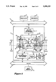
- FIG. 1 a block diagram overview of an external cache memory and a cache controller (CC) in a multiple processor high performance computer system incorporating the teachings of the present invention are shown.
- a central processor unit (CPU) 2 is interconnected via a CPU bus 4 to an external cache arrangement 5.
- Cache arrangement 5 is controlled by a cache controller (CC) 6, wherein CPU 2, CPU bus 4, cache arrangement 5 and CC 6 form a processor module 10.
- Processor module 10 is in turn is intercoupled via a multiple processor (MP) bus 8 to a main memory arrangement 9, and other processor modules 10.
- CPU 2 further has an internal cache arrangements 3.
- Internal cache arrangement 3 is an integrated on-chip cache structures for CPU 2, and is of substantially smaller size relative to external cache arrangement 5.
- CPU bus 4 is assumed to be of any type suitable to accommodate a high performance processor, but may, as in the case of the present invention, be optimized to operate with a particular processor architecture, in this case the Viking processor designed by Sun Microsystems, Inc., Mountain View, Calif. 94043.
- FIG. 2 a block diagram illustrating the arrangement of CC 6 is shown.
- the integrated address and data CPU bus 4 is connected to a CPU bus interface and control unit 11, which controls access to bus 4 in accordance with an internal arbiter (not shown).
- CPU bus interface and control unit 11 is connected in two-way communication with a CPU command module 13 and a multiple processor (MP) command module 12.
- MP command module 12 processes MP bus 8 requests and replies, and in certain cases snooping requests, sourced from MP bus 8, and replies thereto. Snooping requests will be discussed in more detail below.
- CPU command module 13 processes all incoming commands from CPU 2, and if necessary generates proper commands to permit CPU 2 to gain control of MP bus 8.
- a cache directory 15 is intercoupled to MP command module 12 and CPU command module 13 via a local internal cache directory bus 15. The structure and operation of cache directory 15 will be described in more detail below.
- a bus input buffer (BIBUF) 16 in CC 6 is connected to MP bus 8 via a MP bus interface and control unit 19 to provide buffering of commands sent by devices operating on MP bus 8 to to cache directory 15, and to CPU 2 operating on CPU bus 4.
- BIBUF 16 is also coupled to MP command module 12, thereby transmitting commands directed to CPU 2 and/or cache directory 15.
- a bus output buffer (BOBUF) 17 in CC 6 is coupled to the integrated address and data CPU bus 4 via CPU bus interface and control unit 11 to provide buffering of commands directed by CPU 2 through CC 6 to devices operating on the second bus, e.g., main memory 9.
- BOBUF 17 is also coupled to MP command module 12, thereby transmitting replies issued by MP command module 12 and directed to devices operating on MP bus 8.
- BOBUF 17 consists of two buffer structures: request buffer (REQ) 17a having an input and an output, and reply buffer (RPY) 17b having an input and an output.
- MP bus interface and control unit 19 is interconnected to buffers 16 and 17, and governs data communications with external devices intercoupled to CC 6 over MP bus 8.
- MP bus interface and control unit 19 performs functions analogous to functions performed by CPU bus interface and control unit 11.
- MP bus interface and control unit 19 includes a bus interface unit (not shown), and drivers and receivers (not shown) necessary to send and receive signals from CC 6 to devices intercoupled by MP bus 8, and in particular main memory 9.
- the features described but not shown in reference to MP bus interface and control unit 19 are widely known in the art, and do not require further discussion here.
- a data line 60 is routed from MP bus interface and control unit 19 to the input of BIBUF 16. Further, a second data line 61 is routed from MP bus interface and control unit 19 around BIBUF 16 to MP command module 12. Analogously, a third data line 67 is routed from CPU bus interface and control unit 11 to the input of BOBUF 17, in particular REQ buffer 17a. In addition, a fourth data line 68 is routed from CPU bus interface and control unit 11 around REQ buffer 17a to a local data bus 69 internal to BOBUF 17. A fifth data line 65 extends from MP command module 12 to the input of RPY buffer 17b, with a sixth data line 66 routed around RPY buffer 17b to local data bus 69.
- data line 66 The purpose of data line 66 is to permit bus snooping requests to be routed through CC 6 externally from REQ buffer 17a, without constraining the snoop requests to the command/data datapaths. Because cache 5 (FIG. 1) operates in a shared-memory environment, it is necessary that CC 6 have access to cache status information as it relates to shared blocks. As in prior art designs, CC 6 as configured in the present invention permits devices operating on either bus 4 or 8 to monitor, snoop, or access data from the respective bus to maintain cache consistency.
- CC 6 contains a cache invalidation queue (CIQ) buffer 20 coupled to MP bus interface and control unit 19 for storing physical addresses of cache subblocks affected during read-invalidate and write-invalidate operations issued by CPU 2.
- CIQ cache invalidation queue
- CC 6 in the preferred embodiment supports two different clock frequencies via an asynchronous interface (indicated by dashed line 70) between CPU bus 4 and MP bus 8.
- the asynchronous interface 70 permits buses 4 and 8 to operate at different clock frequencies. Decoupling of the operating clocks permits processor 2 to function at a higher speed than, say a system bus (e.g., MP bus 8).
- system bus e.g., MP bus 8
- CPU bus 4 operates at a higher frequency than MP bus 8 to accommodate the high speed data transmission rates of high performance processor 2.
- Buffers 16 and 17 enable communication between devices operating on CPU bus 4 and devices operating on MP bus 8.
- buffers 16 and 17 are first-in-first-out devices implemented with dual-port register files, operating between the two clock domains CLK1 and CLK2.
- BIBUF buffer 16 is 16 ⁇ 73 bits in size
- REQ request buffer 17a consists of two 10 ⁇ 65 bit structures.
- the RPY reply buffer 17b consists of three 10 ⁇ 65 bit buffers.
- the present invention implements a virtual bus interface (VBI) 22 within the CC 6 to reduce latency of commands directed to CPU 2 operating on the integrated address and data CPU bus 4.
- VBI virtual bus interface
- the VBI receives entries made in the input buffer, whereafter the input buffer is again free to accept incoming commands, particularly bus snooping requests from devices operating on the MP bus 8.
- incoming commands particularly bus snooping requests from devices operating on the MP bus 8.
- FIG. 3 a more detailed illustration of CPU bus interface and control unit 11, including virtual bus interface (VBI) 22, is shown.
- CPU bus interface and control unit 11 includes a CPU bus input/output (I/O) frame unit 21.
- CPU bus I/O frame unit 21 contains all drivers, receivers, and latches for outgoing and incoming signals from bus 4, virtual bus interface 22, a CPU bus arbiter 23, and a CPU bus interface 24.
- Virtual bus interface 22 permits the MP command module 12 to freely write to external cache arrangement 5 (shown in FIG. 1) without requiring arbitration. Rather, VBI 22 provides an illusion of a constantly free CPU bus 4, relieving MP command module 12 from dealing with complexities associated with the CPU bus 4 arbitration protocol.
- VBI 22 in the preferred embodiment consists of a 9 ⁇ 107 bit buffer to buffer up to nine cycles of CPU bus 4 accesses made through VBI 22 by MP command module 12. Snooping requests sourced from bus 8 are handled by VBI 22 in seven clock cycles.
- CPU bus arbiter 23 controls and grants requests for access to CPU bus 4 by processor 2, CPU bus interface 24, or VBI 22.
- CPU bus arbiter 23 also regulates bus protocol used for CPU bus 4.
- CPU bus interface 24 internally latches all input signals received from CPU bus 4 before passing the signals to other devices within CC 6.
- CC 6 controls external cache arrangement 15 for a computer system incorporating multiple CPUs 2, e.g., those contained within several of processor modules 10 interconnected on MP bus 8.
- CC 6 further provides a communications interface between the multiple CPUs 2 and the remainder of the computer system.
- CC 6 can support two different bus systems which use external cache memory structures: MBus-based systems and Dynabus-based systems.
- MBus-based systems CC 6 is directly connected to an MBus configuration (shown as bus 8 in FIGS. 1 and 2).
- CC 6 is connected to an XBus configuration. Because the MBus system is well known, and because the Dynabus system is a packet-switch MP bus whose packet switch operation and characteristics are also well known and described in the art, these bus systems will not be further discussed.
- the external cache arrangement 5 is organized as a direct-map cache.
- the size may be 1 megabyte (MB), or optionally 2 MB in the case of a Dynabus-based system.
- the size of the external cache arrangement is larger in the Dynabus arrangement than in the MBus arrangement, due to the use of larger subblock size in Dynabus bus implementations.
- the specific attributes of the present invention are dependent of the bus system selected, and, therefor, for the balance of this detailed description only the MBus configuration will be described. Further, because the organization of the cache is identical in both bus implementations except for size, the balance of the detailed description will use the 1 MB cache construct.
- CC 6 incorporates the teachings disclosed in the above-referenced concurrently filed related U.S. patent application Ser. No. 07/876,359 entitled “Methods and Apparatus for Providing Multiple Pending Operations in a Cache Consistent Multiple Processor Computer System", filed on Apr. 29, 1992, which is hereby incorporated by reference.
- the present invention can support pipelined access to the external cache arrangement 5 from any processor interconnected to CC 6 via CPU bus 4.
- a peak data transfer rate of one double-word (DW) per instruction cycle for both read and write operations is expected.
- DW double-word
- cache directory 15 is constructed as is generally known in the art, having a multiplicity of tag entries 30. There is one entry for each block in the cache arrangement 5. As set out above, the cache arrangement 5 in the preferred embodiment consists of nominally 8K blocks, each 128 B in size. Therefore, cache directory 15 will similarly have 8K tag entries 30.
- Each tag entry 30 consists of an address tag 31, and a multiplicity of status bit fields 32.
- the address tag 31 stores the address tag for the data referenced by the particular block identified by tag entry 30.
- the status bit fields 32 correspond to the subblock present in the block referenced by entry 30. In particular, there is one status bit field 32 for each subblock comprising the block, and there is only a single address tag 31 identifying the several subblocks in that block.
- Each status bit field 32 stores four status bits 33: a p-bit 34, an s-bit 35, an o-bit 36, and a v-bit 37.
- the s-bit 35, o-bit 36, v-bit 37, and p-bit 34 are, respectively, a shared-bit, an owner-bit, an valid-bit, and a pending-bit.
- S-bit 35 when set indicates that the corresponding subblock is shared.
- O-bit 36 when set indicates that a particular CPU 2 executed the most recent write operation.
- V-bit when set indicates the corresponding subblock is valid.
- P-bit 34 when set indicates that an operation assigned by a CPU 2 is pending on the subblock of the block referenced by the index 40 and the subblock index 42.
- P-bit 34 is also set when a prefetch operation is initiated.
- P-bit 34 permits multiple operations to be assigned to subblocks without waiting for completion of previously issued commands, while still only requiring a single address tag to identify all subblocks.
- P-bit 34 prevents access to a subblock for which p-bit 34 is set by enabling CC 6 to require an accessing CPU to relinquish the bus 4, and "retry" the access later.
- CC 6 monitor p-bit 34, CC 6 will permit a subsequent operation on a subblock having p-bit 34 set only when the previous operation is completed and p-bit 34 cleared. If CPU 2 accesses a subblock whose p-bit 34 is not set and the access results in a miss, then the p-bit 34 is first set, a memory access is made to retrieve data to cache arrangement 5, and the address tag bits 31 are updated accordingly.
- CC 6 incorporating the present invention
- CPU 2 operating on CPU bus 4 is shown to issue a write operation at time T 1 , which operation results in a shared-write cache memory access to subblock A, since the issued operation is a write and the share-bit (s-bit) 35 for subblock A is set.
- Pending bit (p-bit) 34 being set indicates that subblock A of cache arrangement 5 has an operation pending.
- a shared-write command and associated subblock address will then be written into BOBUF 17.
- pending completion of the memory access associated with the CPU write operation initiated at T 1 further operations on other subblocks within the same block may still proceed at times subsequent to T 1 .
- a device operating on MP bus 8 arbitrates for and obtains control of bus 8, and thereafter issues some cache invalidating operation directed to subblock A.
- the cache invalidating operation issued by the bus 8 device at time T 2 will invalidate data previously written to subblock A.
- cache invalidation queue (CIQ) buffer 20 enables determining when a prior-occurring cache invalidating instruction has invalidated data in particular cache subblocks, and when cache invalidating operations are to be issued on MP bus 8 to the same subblocks subsequent to bus invalidating operations.
- CIQ buffer 20 stores addresses of cache subblocks to which bus invalidating operations are directed. Because the prior-issued operation is pending and not yet complete, the pending (non-completed) command together with the corresponding block address also will be stored in BOBUF REQ buffer 17a until the necessary destination device address has been fetched from the cache directory 115. Entries stored in BOBUF REQ buffer 17a are compared to entries stored in CIQ buffer 20 via a match logic unit 75.
- CIQ buffer 20 If the address in CIQ buffer 20 matches the address stored in BOBUF REQ buffer 17a, CC 6 will have determined that an intervening cache-invalidating operation has occurred on subblock A, and that the operation directed to the MP bus 8 device must comprise a coherent-read-invalidate (CRI) operation to subblock A, rather than a standard invalidate operation, thus rereading the data.
- CRI coherent-read-invalidate
- An entry in CIQ buffer 20 remain valid unil MP command module 12 indicates the the entry has been invalidated in the cache directory 15.
Abstract
Description
Claims (12)
Priority Applications (3)
| Application Number | Priority Date | Filing Date | Title |
|---|---|---|---|
| US07/879,611 US5398325A (en) | 1992-05-07 | 1992-05-07 | Methods and apparatus for improving cache consistency using a single copy of a cache tag memory in multiple processor computer systems |
| KR1019930006974A KR100278035B1 (en) | 1992-05-07 | 1993-04-26 | Apparatus and method for improving cache consistency using a single copy of cache tag memory in a multiprocessor computer system |
| JP13007493A JP3365433B2 (en) | 1992-05-07 | 1993-05-07 | Cache memory structures and their use |
Applications Claiming Priority (1)
| Application Number | Priority Date | Filing Date | Title |
|---|---|---|---|
| US07/879,611 US5398325A (en) | 1992-05-07 | 1992-05-07 | Methods and apparatus for improving cache consistency using a single copy of a cache tag memory in multiple processor computer systems |
Publications (1)
| Publication Number | Publication Date |
|---|---|
| US5398325A true US5398325A (en) | 1995-03-14 |
Family
ID=25374500
Family Applications (1)
| Application Number | Title | Priority Date | Filing Date |
|---|---|---|---|
| US07/879,611 Expired - Lifetime US5398325A (en) | 1992-05-07 | 1992-05-07 | Methods and apparatus for improving cache consistency using a single copy of a cache tag memory in multiple processor computer systems |
Country Status (3)
| Country | Link |
|---|---|
| US (1) | US5398325A (en) |
| JP (1) | JP3365433B2 (en) |
| KR (1) | KR100278035B1 (en) |
Cited By (72)
| Publication number | Priority date | Publication date | Assignee | Title |
|---|---|---|---|---|
| US5502828A (en) * | 1992-12-18 | 1996-03-26 | Advanced Micro Devices, Inc. | Reducing memory access in a multi-cache multiprocessing environment with each cache mapped into different areas of main memory to avoid contention |
| US5519847A (en) * | 1993-06-30 | 1996-05-21 | Intel Corporation | Method of pipelining sequential writes in a flash memory |
| US5524233A (en) * | 1993-03-31 | 1996-06-04 | Intel Corporation | Method and apparatus for controlling an external cache memory wherein the cache controller is responsive to an interagent communication for performing cache control operations |
| US5526512A (en) * | 1993-09-20 | 1996-06-11 | International Business Machines Corporation | Dynamic management of snoop granularity for a coherent asynchronous DMA cache |
| US5539878A (en) * | 1995-06-16 | 1996-07-23 | Elonex Technologies, Inc. | Parallel testing of CPU cache and instruction units |
| US5581734A (en) * | 1993-08-02 | 1996-12-03 | International Business Machines Corporation | Multiprocessor system with shared cache and data input/output circuitry for transferring data amount greater than system bus capacity |
| US5598551A (en) * | 1993-07-16 | 1997-01-28 | Unisys Corporation | Cache invalidation sequence system utilizing odd and even invalidation queues with shorter invalidation cycles |
| US5603006A (en) * | 1993-09-27 | 1997-02-11 | Hitachi, Ltd. | Cache control unit using a plurality of request stacks |
| US5634043A (en) * | 1994-08-25 | 1997-05-27 | Intel Corporation | Microprocessor point-to-point communication |
| US5642486A (en) * | 1993-07-15 | 1997-06-24 | Unisys Corporation | Invalidation queue with "bit-sliceability" |
| US5655100A (en) * | 1995-03-31 | 1997-08-05 | Sun Microsystems, Inc. | Transaction activation processor for controlling memory transaction execution in a packet switched cache coherent multiprocessor system |
| US5657472A (en) * | 1995-03-31 | 1997-08-12 | Sun Microsystems, Inc. | Memory transaction execution system and method for multiprocessor system having independent parallel transaction queues associated with each processor |
| US5680575A (en) * | 1992-02-20 | 1997-10-21 | International Business Machines Corporation | Interconnect failure detection and cache reset apparatus |
| US5689680A (en) * | 1993-07-15 | 1997-11-18 | Unisys Corp. | Cache memory system and method for accessing a coincident cache with a bit-sliced architecture |
| US5692153A (en) * | 1995-03-16 | 1997-11-25 | International Business Machines Corporation | Method and system for verifying execution order within a multiprocessor data processing system |
| US5696937A (en) * | 1995-04-28 | 1997-12-09 | Unisys Corporation | Cache controller utilizing a state machine for controlling invalidations in a network with dual system busses |
| US5717900A (en) * | 1996-01-26 | 1998-02-10 | Unisys Corporation | Adjusting priority cache access operations with multiple level priority states between a central processor and an invalidation queue |
| US5720008A (en) * | 1994-05-25 | 1998-02-17 | Lucent Technologies Inc. | Knowledge base management system with dependency information for procedural tests |
| US5721840A (en) * | 1993-09-20 | 1998-02-24 | Olympus Optical Co., Ltd. | Information processing apparatus incorporating automatic SCSI ID generation |
| US5737756A (en) * | 1995-04-28 | 1998-04-07 | Unisys Corporation | Dual bus computer network using dual busses with dual spy modules enabling clearing of invalidation queue for processor with store through cache while providing retry cycles for incomplete accesses to invalidation queue |
| WO1998021659A1 (en) * | 1996-11-13 | 1998-05-22 | Intel Corporation | Data cache with data storage and tag logic with different clocks |
| US5778437A (en) * | 1995-09-25 | 1998-07-07 | International Business Machines Corporation | Invalidation bus optimization for multiprocessors using directory-based cache coherence protocols in which an address of a line to be modified is placed on the invalidation bus simultaneously with sending a modify request to the directory |
| US5787476A (en) * | 1995-05-05 | 1998-07-28 | Silicon Graphics, Inc. | System and method for maintaining coherency of virtual-to-physical memory translations in a multiprocessor computer |
| US5809514A (en) * | 1997-02-26 | 1998-09-15 | Texas Instruments Incorporated | Microprocessor burst mode data transfer ordering circuitry and method |
| US5809536A (en) * | 1996-12-09 | 1998-09-15 | Intel Corporation, Inc. | Method for reducing the number of coherency cycles within a directory-based cache coherency memory system uitilizing a memory state cache |
| US5809550A (en) * | 1994-09-30 | 1998-09-15 | Intel Corporation | Method and apparatus for pushing a cacheable memory access operation onto a bus controller queue while determining if the cacheable memory access operation hits a cache |
| US5809548A (en) * | 1996-08-30 | 1998-09-15 | International Business Machines Corporation | System and method for zeroing pages with cache line invalidate instructions in an LRU system having data cache with time tags |
| US5822755A (en) * | 1996-01-25 | 1998-10-13 | International Business Machines Corporation | Dual usage memory selectively behaving as a victim cache for L1 cache or as a tag array for L2 cache |
| US5829039A (en) * | 1994-06-01 | 1998-10-27 | Fujitsu Limited | Memory control method/device for maintaining cache consistency with status bit indicating that a command is being processed with respect to a memory area |
| US5829029A (en) * | 1996-12-18 | 1998-10-27 | Bull Hn Information Systems Inc. | Private cache miss and access management in a multiprocessor system with shared memory |
| US5845310A (en) * | 1993-12-15 | 1998-12-01 | Hewlett-Packard Co. | System and methods for performing cache latency diagnostics in scalable parallel processing architectures including calculating CPU idle time and counting number of cache misses |
| US5848434A (en) * | 1996-12-09 | 1998-12-08 | Intel Corporation | Method and apparatus for caching state information within a directory-based coherency memory system |
| EP0905627A1 (en) * | 1997-09-30 | 1999-03-31 | Sun Microsystems, Inc. | Reducing bandwidth and areas needed for non-inclusive memory hierachy by using dual tags |
| US5893147A (en) * | 1994-12-22 | 1999-04-06 | Intel Corporation | Method and apparatus for distinguishing system memory data from alternative memory data in a shared cache memory |
| US5897656A (en) * | 1996-09-16 | 1999-04-27 | Corollary, Inc. | System and method for maintaining memory coherency in a computer system having multiple system buses |
| US5900020A (en) * | 1996-06-27 | 1999-05-04 | Sequent Computer Systems, Inc. | Method and apparatus for maintaining an order of write operations by processors in a multiprocessor computer to maintain memory consistency |
| US5963973A (en) * | 1996-12-16 | 1999-10-05 | Bull Hn Information Systems Inc. | Multiprocessor computer system incorporating method and apparatus for dynamically assigning ownership of changeable data |
| US6006309A (en) * | 1996-12-16 | 1999-12-21 | Bull Hn Information Systems Inc. | Information block transfer management in a multiprocessor computer system employing private caches for individual center processor units and a shared cache |
| US6018465A (en) * | 1996-12-31 | 2000-01-25 | Intel Corporation | Apparatus for mounting a chip package to a chassis of a computer |
| US6021474A (en) * | 1996-08-26 | 2000-02-01 | International Business Machines Corporation | Apparatus and method of snooping processors and look-aside caches |
| US6029204A (en) * | 1997-03-13 | 2000-02-22 | International Business Machines Corporation | Precise synchronization mechanism for SMP system buses using tagged snoop operations to avoid retries |
| US6049849A (en) * | 1997-04-14 | 2000-04-11 | International Business Machines Corporation | Imprecise method and system for selecting an alternative cache entry for replacement in response to a conflict between cache operation requests |
| US6049847A (en) * | 1996-09-16 | 2000-04-11 | Corollary, Inc. | System and method for maintaining memory coherency in a computer system having multiple system buses |
| US6052762A (en) * | 1996-12-02 | 2000-04-18 | International Business Machines Corp. | Method and apparatus for reducing system snoop latency |
| US6105112A (en) * | 1997-04-14 | 2000-08-15 | International Business Machines Corporation | Dynamic folding of cache operations for multiple coherency-size systems |
| US6137688A (en) * | 1996-12-31 | 2000-10-24 | Intel Corporation | Apparatus for retrofit mounting a VLSI chip to a computer chassis for current supply |
| US6145057A (en) * | 1997-04-14 | 2000-11-07 | International Business Machines Corporation | Precise method and system for selecting an alternative cache entry for replacement in response to a conflict between cache operation requests |
| US6163830A (en) * | 1998-01-26 | 2000-12-19 | Intel Corporation | Method and apparatus to identify a storage device within a digital system |
| US6170030B1 (en) * | 1998-01-23 | 2001-01-02 | Intel Corporation | Method and apparatus for restreaming data that has been queued in a bus bridging device |
| US6223260B1 (en) * | 1996-01-25 | 2001-04-24 | Unisys Corporation | Multi-bus data processing system in which all data words in high level cache memories have any one of four states and all data words in low level cache memories have any one of three states |
| US6253291B1 (en) | 1998-02-13 | 2001-06-26 | Sun Microsystems, Inc. | Method and apparatus for relaxing the FIFO ordering constraint for memory accesses in a multi-processor asynchronous cache system |
| US6336169B1 (en) * | 1999-11-09 | 2002-01-01 | International Business Machines Corporation | Background kill system bus transaction to optimize coherency transactions on a multiprocessor system bus |
| US6463506B1 (en) * | 2000-04-29 | 2002-10-08 | Hewlett-Packard Company | Arrangement of data within cache lines so that tags are first data received |
| US6493809B1 (en) | 2000-01-28 | 2002-12-10 | International Business Machines Corporation | Maintaining order of write operations in a multiprocessor for memory consistency |
| US6622224B1 (en) * | 1997-12-29 | 2003-09-16 | Micron Technology, Inc. | Internal buffered bus for a drum |
| US6662216B1 (en) * | 1997-04-14 | 2003-12-09 | International Business Machines Corporation | Fixed bus tags for SMP buses |
| EP1454253A2 (en) * | 1997-12-19 | 2004-09-08 | Bull HN Information Systems Inc. | Private cache miss and access management in a multiprocessor computer system employing private caches for individual central processor units and a shared cache |
| US20050108481A1 (en) * | 2003-11-17 | 2005-05-19 | Iyengar Arun K. | System and method for achieving strong data consistency |
| US20050105350A1 (en) * | 2003-11-13 | 2005-05-19 | David Zimmerman | Memory channel test fixture and method |
| US20050228926A1 (en) * | 2004-04-05 | 2005-10-13 | Smith Zachary S | Virtual-bus interface and associated system and method |
| US7099998B1 (en) * | 2000-03-31 | 2006-08-29 | Intel Corporation | Method for reducing an importance level of a cache line |
| US20060294274A1 (en) * | 2005-06-23 | 2006-12-28 | Bennett Joseph A | Mechanism for synchronizing controllers for enhanced platform power management |
| US20070162700A1 (en) * | 2005-12-16 | 2007-07-12 | Microsoft Corporation | Optimizing write and wear performance for a memory |
| US20070233909A1 (en) * | 2006-03-30 | 2007-10-04 | Derr Michael N | Power-optimized frame synchronization for multiple USB controllers with non-uniform frame rates |
| US20080313411A1 (en) * | 2006-02-28 | 2008-12-18 | Sugizaki Gou | System controller and cache control method |
| US20090150611A1 (en) * | 2007-12-10 | 2009-06-11 | Microsoft Corporation | Management of external memory functioning as virtual cache |
| US20100070701A1 (en) * | 2008-09-15 | 2010-03-18 | Microsoft Corporation | Managing cache data and metadata |
| US8489815B2 (en) | 2008-09-15 | 2013-07-16 | Microsoft Corporation | Managing cache data and metadata |
| US8909861B2 (en) | 2004-10-21 | 2014-12-09 | Microsoft Corporation | Using external memory devices to improve system performance |
| US20150169452A1 (en) * | 2013-12-16 | 2015-06-18 | Arm Limited | Invalidation of index items for a temporary data store |
| US9361183B2 (en) | 2008-09-19 | 2016-06-07 | Microsoft Technology Licensing, Llc | Aggregation of write traffic to a data store |
| US10216637B2 (en) | 2004-05-03 | 2019-02-26 | Microsoft Technology Licensing, Llc | Non-volatile memory cache performance improvement |
Families Citing this family (2)
| Publication number | Priority date | Publication date | Assignee | Title |
|---|---|---|---|---|
| US6745369B1 (en) * | 2000-06-12 | 2004-06-01 | Altera Corporation | Bus architecture for system on a chip |
| US9727468B2 (en) * | 2004-09-09 | 2017-08-08 | Intel Corporation | Resolving multi-core shared cache access conflicts |
Citations (5)
| Publication number | Priority date | Publication date | Assignee | Title |
|---|---|---|---|---|
| US5148536A (en) * | 1988-07-25 | 1992-09-15 | Digital Equipment Corporation | Pipeline having an integral cache which processes cache misses and loads data in parallel |
| US5201041A (en) * | 1988-12-29 | 1993-04-06 | International Business Machines Corporation | Cache bypass apparatus |
| US5222223A (en) * | 1989-02-03 | 1993-06-22 | Digital Equipment Corporation | Method and apparatus for ordering and queueing multiple memory requests |
| US5228135A (en) * | 1990-01-25 | 1993-07-13 | Kabushiki Kaisha Toshiba | Multiport cache memory control unit including a tag memory having plural address ports and a snoop address part |
| US5265233A (en) * | 1991-05-17 | 1993-11-23 | Sun Microsystems, Inc. | Method and apparatus for providing total and partial store ordering for a memory in multi-processor system |
-
1992
- 1992-05-07 US US07/879,611 patent/US5398325A/en not_active Expired - Lifetime
-
1993
- 1993-04-26 KR KR1019930006974A patent/KR100278035B1/en not_active IP Right Cessation
- 1993-05-07 JP JP13007493A patent/JP3365433B2/en not_active Expired - Lifetime
Patent Citations (5)
| Publication number | Priority date | Publication date | Assignee | Title |
|---|---|---|---|---|
| US5148536A (en) * | 1988-07-25 | 1992-09-15 | Digital Equipment Corporation | Pipeline having an integral cache which processes cache misses and loads data in parallel |
| US5201041A (en) * | 1988-12-29 | 1993-04-06 | International Business Machines Corporation | Cache bypass apparatus |
| US5222223A (en) * | 1989-02-03 | 1993-06-22 | Digital Equipment Corporation | Method and apparatus for ordering and queueing multiple memory requests |
| US5228135A (en) * | 1990-01-25 | 1993-07-13 | Kabushiki Kaisha Toshiba | Multiport cache memory control unit including a tag memory having plural address ports and a snoop address part |
| US5265233A (en) * | 1991-05-17 | 1993-11-23 | Sun Microsystems, Inc. | Method and apparatus for providing total and partial store ordering for a memory in multi-processor system |
Cited By (108)
| Publication number | Priority date | Publication date | Assignee | Title |
|---|---|---|---|---|
| US5680575A (en) * | 1992-02-20 | 1997-10-21 | International Business Machines Corporation | Interconnect failure detection and cache reset apparatus |
| US5502828A (en) * | 1992-12-18 | 1996-03-26 | Advanced Micro Devices, Inc. | Reducing memory access in a multi-cache multiprocessing environment with each cache mapped into different areas of main memory to avoid contention |
| US5737564A (en) * | 1992-12-18 | 1998-04-07 | Advanced Micro Devices, Inc. | Cache memory system having multiple caches with each cache mapped to a different area of main memory to avoid memory contention and to lessen the number of cache snoops |
| US5524233A (en) * | 1993-03-31 | 1996-06-04 | Intel Corporation | Method and apparatus for controlling an external cache memory wherein the cache controller is responsive to an interagent communication for performing cache control operations |
| US5519847A (en) * | 1993-06-30 | 1996-05-21 | Intel Corporation | Method of pipelining sequential writes in a flash memory |
| US5642486A (en) * | 1993-07-15 | 1997-06-24 | Unisys Corporation | Invalidation queue with "bit-sliceability" |
| US5991853A (en) * | 1993-07-15 | 1999-11-23 | Unisys Corporation | Methods for accessing coincident cache with a bit-sliced architecture |
| US6070166A (en) * | 1993-07-15 | 2000-05-30 | Unisys Corporation | Apparatus and method for compressing a plurality of contiguous addresses to form a compressed block address using the first address of the contiguous addresses and a block identifier bit |
| US5689680A (en) * | 1993-07-15 | 1997-11-18 | Unisys Corp. | Cache memory system and method for accessing a coincident cache with a bit-sliced architecture |
| US5598551A (en) * | 1993-07-16 | 1997-01-28 | Unisys Corporation | Cache invalidation sequence system utilizing odd and even invalidation queues with shorter invalidation cycles |
| US5581734A (en) * | 1993-08-02 | 1996-12-03 | International Business Machines Corporation | Multiprocessor system with shared cache and data input/output circuitry for transferring data amount greater than system bus capacity |
| US5721840A (en) * | 1993-09-20 | 1998-02-24 | Olympus Optical Co., Ltd. | Information processing apparatus incorporating automatic SCSI ID generation |
| US5526512A (en) * | 1993-09-20 | 1996-06-11 | International Business Machines Corporation | Dynamic management of snoop granularity for a coherent asynchronous DMA cache |
| US5603006A (en) * | 1993-09-27 | 1997-02-11 | Hitachi, Ltd. | Cache control unit using a plurality of request stacks |
| US5845310A (en) * | 1993-12-15 | 1998-12-01 | Hewlett-Packard Co. | System and methods for performing cache latency diagnostics in scalable parallel processing architectures including calculating CPU idle time and counting number of cache misses |
| US5720008A (en) * | 1994-05-25 | 1998-02-17 | Lucent Technologies Inc. | Knowledge base management system with dependency information for procedural tests |
| US5829039A (en) * | 1994-06-01 | 1998-10-27 | Fujitsu Limited | Memory control method/device for maintaining cache consistency with status bit indicating that a command is being processed with respect to a memory area |
| US5634043A (en) * | 1994-08-25 | 1997-05-27 | Intel Corporation | Microprocessor point-to-point communication |
| US5809550A (en) * | 1994-09-30 | 1998-09-15 | Intel Corporation | Method and apparatus for pushing a cacheable memory access operation onto a bus controller queue while determining if the cacheable memory access operation hits a cache |
| US5893147A (en) * | 1994-12-22 | 1999-04-06 | Intel Corporation | Method and apparatus for distinguishing system memory data from alternative memory data in a shared cache memory |
| US5692153A (en) * | 1995-03-16 | 1997-11-25 | International Business Machines Corporation | Method and system for verifying execution order within a multiprocessor data processing system |
| US5657472A (en) * | 1995-03-31 | 1997-08-12 | Sun Microsystems, Inc. | Memory transaction execution system and method for multiprocessor system having independent parallel transaction queues associated with each processor |
| US5655100A (en) * | 1995-03-31 | 1997-08-05 | Sun Microsystems, Inc. | Transaction activation processor for controlling memory transaction execution in a packet switched cache coherent multiprocessor system |
| US5696937A (en) * | 1995-04-28 | 1997-12-09 | Unisys Corporation | Cache controller utilizing a state machine for controlling invalidations in a network with dual system busses |
| US5737756A (en) * | 1995-04-28 | 1998-04-07 | Unisys Corporation | Dual bus computer network using dual busses with dual spy modules enabling clearing of invalidation queue for processor with store through cache while providing retry cycles for incomplete accesses to invalidation queue |
| US6182195B1 (en) | 1995-05-05 | 2001-01-30 | Silicon Graphics, Inc. | System and method for maintaining coherency of virtual-to-physical memory translations in a multiprocessor computer |
| US5787476A (en) * | 1995-05-05 | 1998-07-28 | Silicon Graphics, Inc. | System and method for maintaining coherency of virtual-to-physical memory translations in a multiprocessor computer |
| WO1997000478A1 (en) * | 1995-06-16 | 1997-01-03 | Elonex Software Solutions, Inc. | Parallel testing of cpu cache and instruction units |
| US5940588A (en) * | 1995-06-16 | 1999-08-17 | Kikinis; Dan | Parallel testing of CPU cache and instruction units |
| US5539878A (en) * | 1995-06-16 | 1996-07-23 | Elonex Technologies, Inc. | Parallel testing of CPU cache and instruction units |
| US5778437A (en) * | 1995-09-25 | 1998-07-07 | International Business Machines Corporation | Invalidation bus optimization for multiprocessors using directory-based cache coherence protocols in which an address of a line to be modified is placed on the invalidation bus simultaneously with sending a modify request to the directory |
| US5822755A (en) * | 1996-01-25 | 1998-10-13 | International Business Machines Corporation | Dual usage memory selectively behaving as a victim cache for L1 cache or as a tag array for L2 cache |
| US6223260B1 (en) * | 1996-01-25 | 2001-04-24 | Unisys Corporation | Multi-bus data processing system in which all data words in high level cache memories have any one of four states and all data words in low level cache memories have any one of three states |
| US5717900A (en) * | 1996-01-26 | 1998-02-10 | Unisys Corporation | Adjusting priority cache access operations with multiple level priority states between a central processor and an invalidation queue |
| US5900020A (en) * | 1996-06-27 | 1999-05-04 | Sequent Computer Systems, Inc. | Method and apparatus for maintaining an order of write operations by processors in a multiprocessor computer to maintain memory consistency |
| US6021474A (en) * | 1996-08-26 | 2000-02-01 | International Business Machines Corporation | Apparatus and method of snooping processors and look-aside caches |
| US5809548A (en) * | 1996-08-30 | 1998-09-15 | International Business Machines Corporation | System and method for zeroing pages with cache line invalidate instructions in an LRU system having data cache with time tags |
| EP1021768A4 (en) * | 1996-09-16 | 2002-08-14 | Corollary Inc | System and method for maintaining memory coherency in a computer system having multiple system buses |
| US5897656A (en) * | 1996-09-16 | 1999-04-27 | Corollary, Inc. | System and method for maintaining memory coherency in a computer system having multiple system buses |
| US6622214B1 (en) | 1996-09-16 | 2003-09-16 | Intel Corporation | System and method for maintaining memory coherency in a computer system having multiple system buses |
| EP1021768A1 (en) * | 1996-09-16 | 2000-07-26 | Corollary, Inc. | System and method for maintaining memory coherency in a computer system having multiple system buses |
| US6049847A (en) * | 1996-09-16 | 2000-04-11 | Corollary, Inc. | System and method for maintaining memory coherency in a computer system having multiple system buses |
| WO1998021659A1 (en) * | 1996-11-13 | 1998-05-22 | Intel Corporation | Data cache with data storage and tag logic with different clocks |
| GB2333621A (en) * | 1996-11-13 | 1999-07-28 | Intel Corp | Data cache with data storage and tag logic with different clocks |
| US7100012B2 (en) * | 1996-11-13 | 2006-08-29 | Intel Corporation | Processor and data cache with data storage unit and tag hit/miss logic operated at a first and second clock frequencies |
| GB2333621B (en) * | 1996-11-13 | 2001-11-21 | Intel Corp | Data cache with data storage and tag logic with different clocks |
| US6631454B1 (en) * | 1996-11-13 | 2003-10-07 | Intel Corporation | Processor and data cache with data storage unit and tag hit/miss logic operated at a first and second clock frequencies |
| US6052762A (en) * | 1996-12-02 | 2000-04-18 | International Business Machines Corp. | Method and apparatus for reducing system snoop latency |
| US5848434A (en) * | 1996-12-09 | 1998-12-08 | Intel Corporation | Method and apparatus for caching state information within a directory-based coherency memory system |
| US5809536A (en) * | 1996-12-09 | 1998-09-15 | Intel Corporation, Inc. | Method for reducing the number of coherency cycles within a directory-based cache coherency memory system uitilizing a memory state cache |
| US6006309A (en) * | 1996-12-16 | 1999-12-21 | Bull Hn Information Systems Inc. | Information block transfer management in a multiprocessor computer system employing private caches for individual center processor units and a shared cache |
| US5963973A (en) * | 1996-12-16 | 1999-10-05 | Bull Hn Information Systems Inc. | Multiprocessor computer system incorporating method and apparatus for dynamically assigning ownership of changeable data |
| WO1999032955A3 (en) * | 1996-12-18 | 2004-07-01 | Bull Hn Information Syst | Private cache miss and access management in a multiprocessor system with shared memory |
| US5829029A (en) * | 1996-12-18 | 1998-10-27 | Bull Hn Information Systems Inc. | Private cache miss and access management in a multiprocessor system with shared memory |
| WO1999032955A2 (en) * | 1996-12-18 | 1999-07-01 | Bull Hn Information Systems Inc. | Private cache miss and access management in a multiprocessor system with shared memory |
| US6137688A (en) * | 1996-12-31 | 2000-10-24 | Intel Corporation | Apparatus for retrofit mounting a VLSI chip to a computer chassis for current supply |
| US6462943B1 (en) | 1996-12-31 | 2002-10-08 | Intel Corporation | Method and apparatus for retrofit mounting a VLSI chip to a computer chassis for current supply |
| US6018465A (en) * | 1996-12-31 | 2000-01-25 | Intel Corporation | Apparatus for mounting a chip package to a chassis of a computer |
| US5809514A (en) * | 1997-02-26 | 1998-09-15 | Texas Instruments Incorporated | Microprocessor burst mode data transfer ordering circuitry and method |
| US6029204A (en) * | 1997-03-13 | 2000-02-22 | International Business Machines Corporation | Precise synchronization mechanism for SMP system buses using tagged snoop operations to avoid retries |
| US6105112A (en) * | 1997-04-14 | 2000-08-15 | International Business Machines Corporation | Dynamic folding of cache operations for multiple coherency-size systems |
| US6145057A (en) * | 1997-04-14 | 2000-11-07 | International Business Machines Corporation | Precise method and system for selecting an alternative cache entry for replacement in response to a conflict between cache operation requests |
| US6662216B1 (en) * | 1997-04-14 | 2003-12-09 | International Business Machines Corporation | Fixed bus tags for SMP buses |
| US6049849A (en) * | 1997-04-14 | 2000-04-11 | International Business Machines Corporation | Imprecise method and system for selecting an alternative cache entry for replacement in response to a conflict between cache operation requests |
| EP0905627A1 (en) * | 1997-09-30 | 1999-03-31 | Sun Microsystems, Inc. | Reducing bandwidth and areas needed for non-inclusive memory hierachy by using dual tags |
| US6073212A (en) * | 1997-09-30 | 2000-06-06 | Sun Microsystems, Inc. | Reducing bandwidth and areas needed for non-inclusive memory hierarchy by using dual tags |
| EP1454253A4 (en) * | 1997-12-19 | 2010-12-29 | Bull Hn Information Syst | Private cache miss and access management in a multiprocessor computer system employing private caches for individual central processor units and a shared cache |
| EP1454253A2 (en) * | 1997-12-19 | 2004-09-08 | Bull HN Information Systems Inc. | Private cache miss and access management in a multiprocessor computer system employing private caches for individual central processor units and a shared cache |
| US6622224B1 (en) * | 1997-12-29 | 2003-09-16 | Micron Technology, Inc. | Internal buffered bus for a drum |
| US6170030B1 (en) * | 1998-01-23 | 2001-01-02 | Intel Corporation | Method and apparatus for restreaming data that has been queued in a bus bridging device |
| US6163830A (en) * | 1998-01-26 | 2000-12-19 | Intel Corporation | Method and apparatus to identify a storage device within a digital system |
| US6253291B1 (en) | 1998-02-13 | 2001-06-26 | Sun Microsystems, Inc. | Method and apparatus for relaxing the FIFO ordering constraint for memory accesses in a multi-processor asynchronous cache system |
| US6336169B1 (en) * | 1999-11-09 | 2002-01-01 | International Business Machines Corporation | Background kill system bus transaction to optimize coherency transactions on a multiprocessor system bus |
| US6493809B1 (en) | 2000-01-28 | 2002-12-10 | International Business Machines Corporation | Maintaining order of write operations in a multiprocessor for memory consistency |
| US7099998B1 (en) * | 2000-03-31 | 2006-08-29 | Intel Corporation | Method for reducing an importance level of a cache line |
| US7028150B2 (en) | 2000-04-29 | 2006-04-11 | Hewlett-Packard Development Company, L.P. | Arrangement of data within cache lines so that tags are first data received |
| US6463506B1 (en) * | 2000-04-29 | 2002-10-08 | Hewlett-Packard Company | Arrangement of data within cache lines so that tags are first data received |
| US20050105350A1 (en) * | 2003-11-13 | 2005-05-19 | David Zimmerman | Memory channel test fixture and method |
| US7177211B2 (en) * | 2003-11-13 | 2007-02-13 | Intel Corporation | Memory channel test fixture and method |
| US20050108481A1 (en) * | 2003-11-17 | 2005-05-19 | Iyengar Arun K. | System and method for achieving strong data consistency |
| US20050228926A1 (en) * | 2004-04-05 | 2005-10-13 | Smith Zachary S | Virtual-bus interface and associated system and method |
| FR2870369A1 (en) * | 2004-04-05 | 2005-11-18 | Hewlett Packard Development Co | VIRTUAL BUS INTERFACE AND ASSOCIATED SYSTEM AND METHOD |
| US10216637B2 (en) | 2004-05-03 | 2019-02-26 | Microsoft Technology Licensing, Llc | Non-volatile memory cache performance improvement |
| US8909861B2 (en) | 2004-10-21 | 2014-12-09 | Microsoft Corporation | Using external memory devices to improve system performance |
| US9690496B2 (en) | 2004-10-21 | 2017-06-27 | Microsoft Technology Licensing, Llc | Using external memory devices to improve system performance |
| US9317209B2 (en) | 2004-10-21 | 2016-04-19 | Microsoft Technology Licensing, Llc | Using external memory devices to improve system performance |
| US20060294274A1 (en) * | 2005-06-23 | 2006-12-28 | Bennett Joseph A | Mechanism for synchronizing controllers for enhanced platform power management |
| US7689745B2 (en) * | 2005-06-23 | 2010-03-30 | Intel Corporation | Mechanism for synchronizing controllers for enhanced platform power management |
| US20070162700A1 (en) * | 2005-12-16 | 2007-07-12 | Microsoft Corporation | Optimizing write and wear performance for a memory |
| US11334484B2 (en) | 2005-12-16 | 2022-05-17 | Microsoft Technology Licensing, Llc | Optimizing write and wear performance for a memory |
| US9529716B2 (en) | 2005-12-16 | 2016-12-27 | Microsoft Technology Licensing, Llc | Optimizing write and wear performance for a memory |
| US8914557B2 (en) | 2005-12-16 | 2014-12-16 | Microsoft Corporation | Optimizing write and wear performance for a memory |
| US8327081B2 (en) | 2006-02-28 | 2012-12-04 | Fujitsu Limited | Information processing device and method for controlling the same |
| US20080313411A1 (en) * | 2006-02-28 | 2008-12-18 | Sugizaki Gou | System controller and cache control method |
| US8069294B2 (en) | 2006-03-30 | 2011-11-29 | Intel Corporation | Power-optimized frame synchronization for multiple USB controllers with non-uniform frame rates |
| US8347015B2 (en) | 2006-03-30 | 2013-01-01 | Intel Corporation | Power-optimized frame synchronization for multiple USB controllers with non-uniform frame rates |
| US20070233909A1 (en) * | 2006-03-30 | 2007-10-04 | Derr Michael N | Power-optimized frame synchronization for multiple USB controllers with non-uniform frame rates |
| US20090150611A1 (en) * | 2007-12-10 | 2009-06-11 | Microsoft Corporation | Management of external memory functioning as virtual cache |
| US8631203B2 (en) | 2007-12-10 | 2014-01-14 | Microsoft Corporation | Management of external memory functioning as virtual cache |
| US9032151B2 (en) | 2008-09-15 | 2015-05-12 | Microsoft Technology Licensing, Llc | Method and system for ensuring reliability of cache data and metadata subsequent to a reboot |
| US20100070701A1 (en) * | 2008-09-15 | 2010-03-18 | Microsoft Corporation | Managing cache data and metadata |
| US10387313B2 (en) | 2008-09-15 | 2019-08-20 | Microsoft Technology Licensing, Llc | Method and system for ensuring reliability of cache data and metadata subsequent to a reboot |
| US8489815B2 (en) | 2008-09-15 | 2013-07-16 | Microsoft Corporation | Managing cache data and metadata |
| US9448890B2 (en) | 2008-09-19 | 2016-09-20 | Microsoft Technology Licensing, Llc | Aggregation of write traffic to a data store |
| US9361183B2 (en) | 2008-09-19 | 2016-06-07 | Microsoft Technology Licensing, Llc | Aggregation of write traffic to a data store |
| US10509730B2 (en) | 2008-09-19 | 2019-12-17 | Microsoft Technology Licensing, Llc | Aggregation of write traffic to a data store |
| US9471493B2 (en) * | 2013-12-16 | 2016-10-18 | Arm Limited | Invalidation of index items for a temporary data store |
| US20150169452A1 (en) * | 2013-12-16 | 2015-06-18 | Arm Limited | Invalidation of index items for a temporary data store |
Also Published As
| Publication number | Publication date |
|---|---|
| KR930023805A (en) | 1993-12-21 |
| KR100278035B1 (en) | 2001-01-15 |
| JPH06131263A (en) | 1994-05-13 |
| JP3365433B2 (en) | 2003-01-14 |
Similar Documents
| Publication | Publication Date | Title |
|---|---|---|
| US5398325A (en) | Methods and apparatus for improving cache consistency using a single copy of a cache tag memory in multiple processor computer systems | |
| EP0568231B1 (en) | Methods and apparatus for providing multiple outstanding operations in a cache consistent multiple processor computer system | |
| US5642494A (en) | Cache memory with reduced request-blocking | |
| US7120755B2 (en) | Transfer of cache lines on-chip between processing cores in a multi-core system | |
| EP0817073B1 (en) | A multiprocessing system configured to perform efficient write operations | |
| US5623632A (en) | System and method for improving multilevel cache performance in a multiprocessing system | |
| US6366984B1 (en) | Write combining buffer that supports snoop request | |
| CA1322058C (en) | Multi-processor computer systems having shared memory and private cache memories | |
| US5878268A (en) | Multiprocessing system configured to store coherency state within multiple subnodes of a processing node | |
| US5893153A (en) | Method and apparatus for preventing a race condition and maintaining cache coherency in a processor with integrated cache memory and input/output control | |
| US5537575A (en) | System for handling cache memory victim data which transfers data from cache to the interface while CPU performs a cache lookup using cache status information | |
| US7133981B2 (en) | Prioritized bus request scheduling mechanism for processing devices | |
| US5848254A (en) | Multiprocessing system using an access to a second memory space to initiate software controlled data prefetch into a first address space | |
| JP3218317B2 (en) | Integrated cache unit and configuration method thereof | |
| US6542968B1 (en) | System and method for managing data in an I/O cache | |
| US5765196A (en) | System and method for servicing copyback requests in a multiprocessor system with a shared memory | |
| JP2000250812A (en) | Memory cache system and managing method therefor | |
| KR100613817B1 (en) | Method and apparatus for the utilization of distributed caches | |
| US5269009A (en) | Processor system with improved memory transfer means | |
| US20020188821A1 (en) | Fast priority determination circuit with rotating priority | |
| US5446844A (en) | Peripheral memory interface controller as a cache for a large data processing system | |
| US6345320B1 (en) | DMA address buffer and cache-memory control system | |
| US6412047B2 (en) | Coherency protocol | |
| US20080307169A1 (en) | Method, Apparatus, System and Program Product Supporting Improved Access Latency for a Sectored Directory | |
| US5678025A (en) | Cache coherency maintenance of non-cache supporting buses |
Legal Events
| Date | Code | Title | Description |
|---|---|---|---|
| AS | Assignment |
Owner name: SUN MICROSYSTEMS, INC. A CORP. OF DELAWARE, CALIF Free format text: ASSIGNMENT OF ASSIGNORS INTEREST.;ASSIGNORS:CHANG, JUNG-HERNG;BERG, CURT;CRUZ-RIOS, JORGE;REEL/FRAME:006126/0294;SIGNING DATES FROM 19920504 TO 19920506 |
|
| STCF | Information on status: patent grant |
Free format text: PATENTED CASE |
|
| FEPP | Fee payment procedure |
Free format text: PAYOR NUMBER ASSIGNED (ORIGINAL EVENT CODE: ASPN); ENTITY STATUS OF PATENT OWNER: LARGE ENTITY |
|
| FPAY | Fee payment |
Year of fee payment: 4 |
|
| CC | Certificate of correction | ||
| FPAY | Fee payment |
Year of fee payment: 8 |
|
| FEPP | Fee payment procedure |
Free format text: PAYER NUMBER DE-ASSIGNED (ORIGINAL EVENT CODE: RMPN); ENTITY STATUS OF PATENT OWNER: LARGE ENTITY Free format text: PAYOR NUMBER ASSIGNED (ORIGINAL EVENT CODE: ASPN); ENTITY STATUS OF PATENT OWNER: LARGE ENTITY |
|
| FPAY | Fee payment |
Year of fee payment: 12 |