US5400220A - Mechanical printed circuit board and ball grid array interconnect apparatus - Google Patents
Mechanical printed circuit board and ball grid array interconnect apparatus Download PDFInfo
- Publication number
- US5400220A US5400220A US08/245,410 US24541094A US5400220A US 5400220 A US5400220 A US 5400220A US 24541094 A US24541094 A US 24541094A US 5400220 A US5400220 A US 5400220A
- Authority
- US
- United States
- Prior art keywords
- circuit board
- metallic coating
- board apparatus
- plate member
- rigid plate
- Prior art date
- Legal status (The legal status is an assumption and is not a legal conclusion. Google has not performed a legal analysis and makes no representation as to the accuracy of the status listed.)
- Expired - Lifetime
Links
Images


Classifications
-
- H—ELECTRICITY
- H05—ELECTRIC TECHNIQUES NOT OTHERWISE PROVIDED FOR
- H05K—PRINTED CIRCUITS; CASINGS OR CONSTRUCTIONAL DETAILS OF ELECTRIC APPARATUS; MANUFACTURE OF ASSEMBLAGES OF ELECTRICAL COMPONENTS
- H05K1/00—Printed circuits
- H05K1/02—Details
- H05K1/11—Printed elements for providing electric connections to or between printed circuits
- H05K1/111—Pads for surface mounting, e.g. lay-out
- H05K1/112—Pads for surface mounting, e.g. lay-out directly combined with via connections
- H05K1/114—Pad being close to via, but not surrounding the via
-
- H—ELECTRICITY
- H05—ELECTRIC TECHNIQUES NOT OTHERWISE PROVIDED FOR
- H05K—PRINTED CIRCUITS; CASINGS OR CONSTRUCTIONAL DETAILS OF ELECTRIC APPARATUS; MANUFACTURE OF ASSEMBLAGES OF ELECTRICAL COMPONENTS
- H05K3/00—Apparatus or processes for manufacturing printed circuits
- H05K3/30—Assembling printed circuits with electric components, e.g. with resistor
- H05K3/32—Assembling printed circuits with electric components, e.g. with resistor electrically connecting electric components or wires to printed circuits
- H05K3/325—Assembling printed circuits with electric components, e.g. with resistor electrically connecting electric components or wires to printed circuits by abutting or pinching, i.e. without alloying process; mechanical auxiliary parts therefor
-
- H—ELECTRICITY
- H05—ELECTRIC TECHNIQUES NOT OTHERWISE PROVIDED FOR
- H05K—PRINTED CIRCUITS; CASINGS OR CONSTRUCTIONAL DETAILS OF ELECTRIC APPARATUS; MANUFACTURE OF ASSEMBLAGES OF ELECTRICAL COMPONENTS
- H05K2201/00—Indexing scheme relating to printed circuits covered by H05K1/00
- H05K2201/09—Shape and layout
- H05K2201/09209—Shape and layout details of conductors
- H05K2201/09372—Pads and lands
- H05K2201/09472—Recessed pad for surface mounting; Recessed electrode of component
-
- H—ELECTRICITY
- H05—ELECTRIC TECHNIQUES NOT OTHERWISE PROVIDED FOR
- H05K—PRINTED CIRCUITS; CASINGS OR CONSTRUCTIONAL DETAILS OF ELECTRIC APPARATUS; MANUFACTURE OF ASSEMBLAGES OF ELECTRICAL COMPONENTS
- H05K2201/00—Indexing scheme relating to printed circuits covered by H05K1/00
- H05K2201/09—Shape and layout
- H05K2201/09209—Shape and layout details of conductors
- H05K2201/095—Conductive through-holes or vias
- H05K2201/09509—Blind vias, i.e. vias having one side closed
-
- H—ELECTRICITY
- H05—ELECTRIC TECHNIQUES NOT OTHERWISE PROVIDED FOR
- H05K—PRINTED CIRCUITS; CASINGS OR CONSTRUCTIONAL DETAILS OF ELECTRIC APPARATUS; MANUFACTURE OF ASSEMBLAGES OF ELECTRICAL COMPONENTS
- H05K2201/00—Indexing scheme relating to printed circuits covered by H05K1/00
- H05K2201/10—Details of components or other objects attached to or integrated in a printed circuit board
- H05K2201/10227—Other objects, e.g. metallic pieces
- H05K2201/10393—Clamping a component by an element or a set of elements
-
- H—ELECTRICITY
- H05—ELECTRIC TECHNIQUES NOT OTHERWISE PROVIDED FOR
- H05K—PRINTED CIRCUITS; CASINGS OR CONSTRUCTIONAL DETAILS OF ELECTRIC APPARATUS; MANUFACTURE OF ASSEMBLAGES OF ELECTRICAL COMPONENTS
- H05K2201/00—Indexing scheme relating to printed circuits covered by H05K1/00
- H05K2201/10—Details of components or other objects attached to or integrated in a printed circuit board
- H05K2201/10613—Details of electrical connections of non-printed components, e.g. special leads
- H05K2201/10621—Components characterised by their electrical contacts
- H05K2201/10734—Ball grid array [BGA]; Bump grid array
-
- H—ELECTRICITY
- H05—ELECTRIC TECHNIQUES NOT OTHERWISE PROVIDED FOR
- H05K—PRINTED CIRCUITS; CASINGS OR CONSTRUCTIONAL DETAILS OF ELECTRIC APPARATUS; MANUFACTURE OF ASSEMBLAGES OF ELECTRICAL COMPONENTS
- H05K2203/00—Indexing scheme relating to apparatus or processes for manufacturing printed circuits covered by H05K3/00
- H05K2203/07—Treatments involving liquids, e.g. plating, rinsing
- H05K2203/0703—Plating
- H05K2203/0723—Electroplating, e.g. finish plating
-
- H—ELECTRICITY
- H05—ELECTRIC TECHNIQUES NOT OTHERWISE PROVIDED FOR
- H05K—PRINTED CIRCUITS; CASINGS OR CONSTRUCTIONAL DETAILS OF ELECTRIC APPARATUS; MANUFACTURE OF ASSEMBLAGES OF ELECTRICAL COMPONENTS
- H05K3/00—Apparatus or processes for manufacturing printed circuits
- H05K3/02—Apparatus or processes for manufacturing printed circuits in which the conductive material is applied to the surface of the insulating support and is thereafter removed from such areas of the surface which are not intended for current conducting or shielding
- H05K3/06—Apparatus or processes for manufacturing printed circuits in which the conductive material is applied to the surface of the insulating support and is thereafter removed from such areas of the surface which are not intended for current conducting or shielding the conductive material being removed chemically or electrolytically, e.g. by photo-etch process
- H05K3/061—Etching masks
- H05K3/062—Etching masks consisting of metals or alloys or metallic inorganic compounds
-
- H—ELECTRICITY
- H05—ELECTRIC TECHNIQUES NOT OTHERWISE PROVIDED FOR
- H05K—PRINTED CIRCUITS; CASINGS OR CONSTRUCTIONAL DETAILS OF ELECTRIC APPARATUS; MANUFACTURE OF ASSEMBLAGES OF ELECTRICAL COMPONENTS
- H05K3/00—Apparatus or processes for manufacturing printed circuits
- H05K3/40—Forming printed elements for providing electric connections to or between printed circuits
- H05K3/42—Plated through-holes or plated via connections
- H05K3/425—Plated through-holes or plated via connections characterised by the sequence of steps for plating the through-holes or via connections in relation to the conductive pattern
- H05K3/426—Plated through-holes or plated via connections characterised by the sequence of steps for plating the through-holes or via connections in relation to the conductive pattern initial plating of through-holes in substrates without metal
-
- H—ELECTRICITY
- H05—ELECTRIC TECHNIQUES NOT OTHERWISE PROVIDED FOR
- H05K—PRINTED CIRCUITS; CASINGS OR CONSTRUCTIONAL DETAILS OF ELECTRIC APPARATUS; MANUFACTURE OF ASSEMBLAGES OF ELECTRICAL COMPONENTS
- H05K3/00—Apparatus or processes for manufacturing printed circuits
- H05K3/46—Manufacturing multilayer circuits
- H05K3/4644—Manufacturing multilayer circuits by building the multilayer layer by layer, i.e. build-up multilayer circuits
-
- Y—GENERAL TAGGING OF NEW TECHNOLOGICAL DEVELOPMENTS; GENERAL TAGGING OF CROSS-SECTIONAL TECHNOLOGIES SPANNING OVER SEVERAL SECTIONS OF THE IPC; TECHNICAL SUBJECTS COVERED BY FORMER USPC CROSS-REFERENCE ART COLLECTIONS [XRACs] AND DIGESTS
- Y10—TECHNICAL SUBJECTS COVERED BY FORMER USPC
- Y10T—TECHNICAL SUBJECTS COVERED BY FORMER US CLASSIFICATION
- Y10T29/00—Metal working
- Y10T29/49—Method of mechanical manufacture
- Y10T29/49002—Electrical device making
- Y10T29/49117—Conductor or circuit manufacturing
- Y10T29/49124—On flat or curved insulated base, e.g., printed circuit, etc.
- Y10T29/4913—Assembling to base an electrical component, e.g., capacitor, etc.
- Y10T29/49139—Assembling to base an electrical component, e.g., capacitor, etc. by inserting component lead or terminal into base aperture
-
- Y—GENERAL TAGGING OF NEW TECHNOLOGICAL DEVELOPMENTS; GENERAL TAGGING OF CROSS-SECTIONAL TECHNOLOGIES SPANNING OVER SEVERAL SECTIONS OF THE IPC; TECHNICAL SUBJECTS COVERED BY FORMER USPC CROSS-REFERENCE ART COLLECTIONS [XRACs] AND DIGESTS
- Y10—TECHNICAL SUBJECTS COVERED BY FORMER USPC
- Y10T—TECHNICAL SUBJECTS COVERED BY FORMER US CLASSIFICATION
- Y10T29/00—Metal working
- Y10T29/49—Method of mechanical manufacture
- Y10T29/49002—Electrical device making
- Y10T29/49117—Conductor or circuit manufacturing
- Y10T29/49124—On flat or curved insulated base, e.g., printed circuit, etc.
- Y10T29/49147—Assembling terminal to base
- Y10T29/49151—Assembling terminal to base by deforming or shaping
- Y10T29/49153—Assembling terminal to base by deforming or shaping with shaping or forcing terminal into base aperture
-
- Y—GENERAL TAGGING OF NEW TECHNOLOGICAL DEVELOPMENTS; GENERAL TAGGING OF CROSS-SECTIONAL TECHNOLOGIES SPANNING OVER SEVERAL SECTIONS OF THE IPC; TECHNICAL SUBJECTS COVERED BY FORMER USPC CROSS-REFERENCE ART COLLECTIONS [XRACs] AND DIGESTS
- Y10—TECHNICAL SUBJECTS COVERED BY FORMER USPC
- Y10T—TECHNICAL SUBJECTS COVERED BY FORMER US CLASSIFICATION
- Y10T29/00—Metal working
- Y10T29/49—Method of mechanical manufacture
- Y10T29/49002—Electrical device making
- Y10T29/49117—Conductor or circuit manufacturing
- Y10T29/49204—Contact or terminal manufacturing
- Y10T29/49208—Contact or terminal manufacturing by assembling plural parts
- Y10T29/49222—Contact or terminal manufacturing by assembling plural parts forming array of contacts or terminals
Definitions
- the present invention relates generally to circuit board construction, and more particularly relates to apparatus and methods for operatively connecting an electronic component ball grid array (“BGA”) to a circuit board.
- BGA ball grid array
- PCBs printed circuit boards
- PCAs printed circuit assemblies
- soldering was performed manually. Subsequently, more efficient machine-soldering techniques employing infrared ovens or solder baths were developed to speed manufacture of circuit boards and to ensure higher solder joint reliability. Under such machine-soldering techniques, the PCB and its components were heated while solder, under the influence of flux, was caused to contact the board and flow by capillary action into the vias, yielding a low resistance solder joint when cooled.
- circuit board technology As circuit board technology developed, designers began to create circuit boards comprising many alternating substrate and conductive layer pairs, resulting in sandwiched circuit boards that could accommodate a higher component density. Such boards could accommodate ten or more conductive layers. Later, surface-mount technology allowed the leads to be soldered to solder pads on the surface of the circuit board, rather than requiring the leads to pass through vias to be soldered therein.
- ICs integrated circuits
- DIPs dual in-line packages
- the leads could either be through-hole soldered or surface-mounted.
- the number of leads that a DIP could accommodate was a function of twice the length of the DIP body edges.
- quad flat packs comprising a generally square body having leads extending downward from the lower surface of the body.
- the leads were typically arranged in multiple rows and columns, allowing the QFPs to accommodate more pins than DIPs.
- limitations in socket size and collective lead insertion force began to be problematical.
- BGA ball grid array
- the BGA package In connecting a BGA electronic component package to the circuit board, the BGA package is typically placed on the appropriate side of the circuit board, using a high accuracy "pick and place” machine, in a manner such that the ball shaped lead portions of the BGA package contact the flat, surface mounted solder pads.
- the partially completed circuit board/BGA package structure is them subjected to an infrared solder reflow process to mechanically and electrically couple the surface pads to the ball shaped lead portions of the BGA package.
- a circuit board is provided with improved apparatus for operatively connecting the circuit board to a BGA package.
- the circuit board includes a substrate structure having first and second opposite sides.
- a spaced series of vias extend transversely through the substrate structure between its opposite first and second sides, and a spaced series of socket areas are offset from the vias and extend only partially through the substrate structure from its first side.
- the vias and socket areas are preferably formed by a precision drilling process.
- An electrically conductive metal coating is deposited on the interiors of the vias and the socket areas and around their open ends of the first substrate side. Mutually spaced portions of the metallic coating extend across the first substrate side between associated via/socket area pairs to electrically couple them.
- the metallic coating has a multi-layer structure in which the inner layer is copper, the outer layer is gold, and an intermediate nickel layer is interposed between the copper and gold layers.
- the coating is representatively formed by an etching process in which gold is used as the etch resist material.
- the metallically coated socket areas are relatively oriented to partially receive a spaced array of generally ball-shaped lead portions externally disposed on the BGA package to be operatively connected to the circuit board.
- the BGA package is positioned along the first substrate side, with the BGA lead portions extending partially into and engaging the metal coating portions of the socket areas.
- Holding means are provided for exerting a resilient force on the BGA package in a manner releasably holding its lead portions in engagement with the metallic coating of their associated socket areas.
- the holding means include first and second elastomeric pad members respectively positioned against the outer side of the BGA package and the second side of the substrate structure, a resiliently compressible spring plate structure positioned against the outer side of the first elastomeric pad member, a rigid backing plate member positioned against the outer side of the second elastomeric pad member, and a series of clamping bolts secured between the spring plate structure and the backing plate and tightened to compress the first and second elastomeric pad members and the spring plate structure.
- the socketed configurations of the BGA connection portions of the circuit board substantially facilitate an automatic registry between the BGA lead portions and such connection portions during the initial placement of the BGA package on the circuit board substrate.
- the socket areas further act to inhibit shifting of the installed BGA package relative to the circuit board substrate while clamped thereto by the holding means.
- the releasable clamping of the BGA package to the circuit board substrate permits the BGA package to be easily removed for repair, replacement or upgrade purposes.
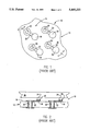
- FIG. 1 is a top plan view of a portion of a conventional circuit board having offset arrays of electrically coupled vias and flat, surface mounted solder pads formed thereon;
- FIG. 2 (PRIOR ART) is a cross-sectional view through the circuit board taken along line 2--2 of FIG. 1:
- FIGS. 3A-3C are simplified cross-sectional views through an improved circuit board embodying principles of the present invention and sequentially illustrating the construction of the board and the operative connection of BGA electronic component structure thereto;
- FIG. 4 is a top plan view of a portion of the partially completed circuit board taken along line 4--4 of FIG. 3A;
- FIG. 5 is an enlargement of the circled area "A" in FIG. 3B.
- FIG. 6 is a reduced scale, partially cut away top plan view of a spring clamp structure shown in FIG. 3.
- connection circuitry 14 includes a spaced array of circular solder pads 18 that are offset from a corresponding spaced array of metallically lined vias 20 and electrically coupled thereto by a series of interstitial electrically conductive surface traces 22.
- the pads 18, as illustrated in FIG. 2 are used as circuit board connection areas for the generally ball-shaped lead portions 24 depending in a mutually spaced, finely-pitched array from the underside of a representative BGA package 26 and arranged to be registrable with the pads 18 on the circuit board substrate 12.
- the package 26 is positioned against the circuit board in a manner such that the ball-shaped leads 24 engage the top sides of the metallic solder pads 18.
- a conventional IR solder reflow process is used to solder the BGA leads 24 to the underlying surface mounted pads 18 as at 28.
- FIGS. 3A-3C sequentially illustrate the formation of an improved circuit board 30 (see FIGS. 3B and 3C) and the operative releasable mechanical connection of the completed circuit board 30 to a representative BGA package 32 having a mutually spaced array of ball-shaped lead portions 34 depending from its underside.
- a unique configuration of the BGA connection portion of the circuit board 30 serves as registration means for facilitating the proper alignment between the BGA leads 34 and the associated connection portion of the circuit board 30.
- the fabrication of the improved circuit board 30 is begun by forming an insulative substrate member 36 that has a top side 38.
- the substrate member 36 is of a laminated construction in which a plurality of interior "tiers" of circuitry portions 40,42 are operatively disposed.
- a spaced series of circularly cross-sectioned vias 44 are formed transversely through the substrate member, between its opposite sides, using precision drilling apparatus. As illustrated, the vias 44 are positioned to intersect facing end sections of selected interior circuit portions 40 and 42.
- a spaced series of relatively shallow, circularly cross-sectioned sockets 46 are formed in the top side 38 of the substrate structure 36.
- the sockets 46 have diameters just slightly larger than the diameters of the BGA lead members 34, are offset from the vias 44, and are positioned on centerlines registrable with the centerlines of the BGA lead members 34.
- each via 44 and its associated adjacent socket 46 are plated with a metallic coating generally denoted by the reference numeral 48.
- the metallic coating 48 preferably comprises a layer of copper 50 (see FIG. 5) deposited directly on the indicated substrate structure surfaces, a layer of nickel 52 deposited on the outer side of the copper layer 50, and a layer of gold 54 deposited on the outer side of the nickel layer 52.
- the copper and nickel layers 50,52 are deposited on the substrate structure using a conventional outer layering process.
- the gold layer 54 is used as the etch resist in place of the conventionally utilized solder (Sn/Pb).
- this creates a gold outer side contact surface on the overall metallic coating 48 which, in a manner subsequently described, is brought into contact with the BGA leads 34 to operatively couple the circuit board 30 to the BGA package 32.
- This permits the overall BGA connection apparatus formed integrally on the circuit board 30 to utilize the superior electrical contact surface finish and interconnection reliability properties of gold.
- the metallic coating 48 extends along the top side 38 of the substrate structure 36 at the open top ends of the vias 44 and the sockets 46, and along the bottom side 50 of the substrate structure 36 around the open bottom ends of the vias 40.
- Interstitial portions 48a of the coating structure 48 extend along the top substrate side 38 between the coating material of each via 44 and the coating material of its associated socket 46.
- the fabrication of the overall circuit board/BGA package assembly shown in FIG. 3C is completed by positioning the BGA package 32 atop the circuit board substrate 36 (using a high accuracy pick and place machine) in a manner such that the BGA leads 34 register with the plated sockets 46 and partially enter them as illustrated in FIG. 3C.
- the BGA package 32 is then mechanically and releasably held in place on the circuit board 30, in a manner permitting the BGA package 32 to be easily removed for replacement and upgrade purposes, using a specially designed resilient clamping structure 56 which will now be described in conjunction with FIGS. 3C and 6.
- Resilient clamping structure 56 includes upper and lower elastomeric pads 58,60 respectively placed along the top side of the BGA package 32 and along the bottom side 50 of the substrate structure 36; a rigid rectangular backing plate 62 extending along the underside of the lower elastomeric pad 60; a rectangular spring plate structure 64 positioned atop the upper elastomeric pad 58, and four elongated clamping bolt members 66 extending through facing corner openings in the backing plate 62 and the spring plate structure 64 and threaded into retaining nuts 68.
- the spring plate structure 64 includes vertically spaced upper and lower parallel rigid plate members 70 and 72 which are in a facing relationship and are movable toward and away from one another. Sandwiched between the plate members 70,72 are a spaced series of vertically oriented coiled compression spring members 74 that are fixed at their upper and lower ends to the facing interior side surfaces of the plates 70,72.
- the use of the spring plate structure 64 compensates for any lateral "relaxation" that may occur in the elastomeric pads 58,60 over time that would tend to undesirably lessening the retaining force on the BGA leads 34 that keeps them in registry and partially received in their associated sockets 46.
- the compressed springs 74 simply expand a bit and automatically drive the plate 72 inwardly toward the sockets 46 to maintain sufficient clamping force on the BGA leads 34.
- the plates 70 and 72 (as well as the elastomeric pad 58) preferably have aligned central rectangular cutout areas 72 formed therein that overlie a central top side portion of the BGA package 32 in the completed circuit board/BGA package assembly.
- This cutout area corresponds with the non-I/O area of the typical BGA package (such as a processor) and may conveniently be used to receive a suitable heat sink device (not shown) operatively connected to the top side of the BGA device 32.
- the use of the plated socket areas 46 in conjunction with the generally ball-shaped lead portions 34 of the BGA package provide a substantial degree of self-alignment between the BGA package 32 and the circuit board substrate 36 during initial placement of the BGA package on the substrate structure. Additionally, the use of the resilient clamping structure 56 maintains the BGA lead portions 34 in firm contact with the metal plating portions of their associated socket areas 46 yet permits the BGA package 32 to be quickly removed and replaced if desired.
- the partial receipt of the BGA lead portions 34 in the plated socket areas 46 serves to prevent shifting of the mechanically clamped lead portions 34 out of their socket areas 46 in a direction parallel to the top side 38 of the substrate portion 36. Further, the outer gold layer 54 on the socket area plating structures 48 provides superior electrical contact characteristics between the leads 34 and the plating structures of the socket areas 46.
- FIG. 3C While the overall circuit board/BGA package assembly shown in FIG. 3C has been shown with a BGA package mounted on its top side, it will be readily appreciated that plated socket areas could also be formed on the bottom side 50 of the substrate 36 and used in conjunction with one or more additional BGA packages mounted on the bottom substrate side and held in place with the resilient clamping structure 56. In such case, an additional spring plate structure 64 could be used in place of the bottom backing plate 62.
Abstract
Description
Claims (23)
Priority Applications (2)
| Application Number | Priority Date | Filing Date | Title |
|---|---|---|---|
| US08/245,410 US5400220A (en) | 1994-05-18 | 1994-05-18 | Mechanical printed circuit board and ball grid array interconnect apparatus |
| US08/275,854 US5587885A (en) | 1994-05-18 | 1994-07-15 | Mechanical printed circuit board/laminated multi chip module interconnect apparatus |
Applications Claiming Priority (1)
| Application Number | Priority Date | Filing Date | Title |
|---|---|---|---|
| US08/245,410 US5400220A (en) | 1994-05-18 | 1994-05-18 | Mechanical printed circuit board and ball grid array interconnect apparatus |
Related Child Applications (1)
| Application Number | Title | Priority Date | Filing Date |
|---|---|---|---|
| US08/275,854 Continuation-In-Part US5587885A (en) | 1994-05-18 | 1994-07-15 | Mechanical printed circuit board/laminated multi chip module interconnect apparatus |
Publications (1)
| Publication Number | Publication Date |
|---|---|
| US5400220A true US5400220A (en) | 1995-03-21 |
Family
ID=22926542
Family Applications (1)
| Application Number | Title | Priority Date | Filing Date |
|---|---|---|---|
| US08/245,410 Expired - Lifetime US5400220A (en) | 1994-05-18 | 1994-05-18 | Mechanical printed circuit board and ball grid array interconnect apparatus |
Country Status (1)
| Country | Link |
|---|---|
| US (1) | US5400220A (en) |
Cited By (57)
| Publication number | Priority date | Publication date | Assignee | Title |
|---|---|---|---|---|
| WO1996027280A1 (en) * | 1995-03-02 | 1996-09-06 | Intel Corporation | Thermally and electrically enhanced ball grid package |
| US5570033A (en) * | 1995-07-20 | 1996-10-29 | Vlsi Technology, Inc. | Spring probe BGA (ball grid array) contactor with device stop and method therefor |
| WO1997023121A1 (en) * | 1995-12-19 | 1997-06-26 | Thermicedge Corporation | Spheres useful in a detachable connective medium for ball grid array assemblies |
| US5670418A (en) * | 1996-12-17 | 1997-09-23 | International Business Machines Corporation | Method of joining an electrical contact element to a substrate |
| US5691245A (en) * | 1996-10-28 | 1997-11-25 | He Holdings, Inc. | Methods of forming two-sided HDMI interconnect structures |
| US5710733A (en) * | 1996-01-22 | 1998-01-20 | Silicon Graphics, Inc. | Processor-inclusive memory module |
| US5714803A (en) * | 1995-07-28 | 1998-02-03 | Sgs-Thomson Microelectronics, Inc. | Low-profile removable ball-grid-array integrated circuit package |
| US5724229A (en) * | 1996-03-27 | 1998-03-03 | Unisys Corporation | Electromechanical assembly having a lid which protects IC chips and holds contact springs |
| US5736789A (en) * | 1994-07-26 | 1998-04-07 | Sgs-Thomson Microelectronics S.A. | Ball grid array casing for integrated circuits |
| US5742481A (en) * | 1995-10-04 | 1998-04-21 | Advanced Interconnections Corporation | Removable terminal support member for integrated circuit socket/adapter assemblies |
| US5764485A (en) * | 1996-04-19 | 1998-06-09 | Lebaschi; Ali | Multi-layer PCB blockade-via pad-connection |
| US5766021A (en) * | 1996-10-01 | 1998-06-16 | Augat Inc. | BGA interconnectors |
| US5784262A (en) * | 1995-11-06 | 1998-07-21 | Symbios, Inc. | Arrangement of pads and through-holes for semiconductor packages |
| US5831444A (en) * | 1996-01-25 | 1998-11-03 | General Dynamics Information Systems, Inc. | Apparatus for performing a function on an integrated circuit |
| US5833472A (en) * | 1995-07-27 | 1998-11-10 | The Whitaker Corporation | Socket assembly for an electronic package |
| US5847936A (en) * | 1997-06-20 | 1998-12-08 | Sun Microsystems, Inc. | Optimized routing scheme for an integrated circuit/printed circuit board |
| US5867419A (en) * | 1997-01-27 | 1999-02-02 | Silicon Graphics, Inc. | Processor-inclusive memory module |
| US5880590A (en) * | 1997-05-07 | 1999-03-09 | International Business Machines Corporation | Apparatus and method for burn-in and testing of devices with solder bumps or preforms |
| US5950072A (en) * | 1997-07-25 | 1999-09-07 | Stmicroelectronics, Inc. | Low-profile removable ball-grid-array integrated circuit package |
| US6023029A (en) * | 1998-03-19 | 2000-02-08 | International Business Machines Corporation | Use of blind vias for soldered interconnections between substrates and printed wiring boards |
| US6037667A (en) * | 1998-08-24 | 2000-03-14 | Micron Technology, Inc. | Socket assembly for use with solder ball |
| DE19840501C1 (en) * | 1998-09-07 | 2000-04-20 | Hitex Systementwicklung Ges Fu | Electrical contact device for mounting microchip on printed circuit board, uses rubber mat with metallised openings receiving contacts of microchip at one side and contacting printed circuit board at opposite side |
| US6054767A (en) * | 1998-01-13 | 2000-04-25 | Lsi Logic Corp. | Programmable substrate for array-type packages |
| US6057600A (en) * | 1997-11-27 | 2000-05-02 | Kyocera Corporation | Structure for mounting a high-frequency package |
| US6125042A (en) * | 1998-04-10 | 2000-09-26 | Lucent Technologies, Inc. | Ball grid array semiconductor package having improved EMI characteristics |
| US6150726A (en) * | 1996-09-06 | 2000-11-21 | International Business Machines Corp. | Component carrier with raised bonding sites |
| WO2001004650A1 (en) * | 1999-07-12 | 2001-01-18 | Pjc Technologies, Inc. | Test probe head having encapsulated rigid pins |
| US6246312B1 (en) | 2000-07-20 | 2001-06-12 | Cts Corporation | Ball grid array resistor terminator network |
| US6253675B1 (en) | 1999-06-29 | 2001-07-03 | Carl P. Mayer | Solder paste stenciling apparatus and method of use for rework |
| WO2001049088A1 (en) * | 1999-12-28 | 2001-07-05 | Intel Corporation | Direct bga attachment without solder reflow |
| US6271111B1 (en) | 1998-02-25 | 2001-08-07 | International Business Machines Corporation | High density pluggable connector array and process thereof |
| US6324754B1 (en) | 1998-03-25 | 2001-12-04 | Tessera, Inc. | Method for fabricating microelectronic assemblies |
| US6329605B1 (en) * | 1998-03-26 | 2001-12-11 | Tessera, Inc. | Components with conductive solder mask layers |
| US6330744B1 (en) | 1999-07-12 | 2001-12-18 | Pjc Technologies, Inc. | Customized electrical test probe head using uniform probe assemblies |
| US6362516B1 (en) | 1997-04-03 | 2002-03-26 | Motorola, Inc. | Electronic apparatus |
| US6388207B1 (en) * | 2000-12-29 | 2002-05-14 | Intel Corporation | Electronic assembly with trench structures and methods of manufacture |
| US6407566B1 (en) | 2000-04-06 | 2002-06-18 | Micron Technology, Inc. | Test module for multi-chip module simulation testing of integrated circuit packages |
| US6413102B2 (en) * | 1999-12-22 | 2002-07-02 | Micron Technology, Inc. | Center bond flip chip semiconductor carrier and a method of making and using it |
| US6440770B1 (en) | 1996-09-09 | 2002-08-27 | Intel Corporation | Integrated circuit package |
| US6456515B1 (en) | 2000-11-27 | 2002-09-24 | Briggs & Stratton Corporation | Three-phase H-bridge assembly and method of assembling the same |
| US6464513B1 (en) | 2000-01-05 | 2002-10-15 | Micron Technology, Inc. | Adapter for non-permanently connecting integrated circuit devices to multi-chip modules and method of using same |
| US6476472B1 (en) | 2000-08-18 | 2002-11-05 | Agere Systems Inc. | Integrated circuit package with improved ESD protection for no-connect pins |
| US20030040139A1 (en) * | 2001-08-21 | 2003-02-27 | Canella Robert L. | Spring contact for establishing non-permanent electrical connection between an integrated circuit device lead element and a substrate, apparatus including same and method of use |
| US20030042595A1 (en) * | 2001-08-29 | 2003-03-06 | Canella Robert L. | Substrate with contact array and substrate assemblies |
| US6544461B1 (en) * | 1998-08-28 | 2003-04-08 | Micron Technology, Inc. | Test carrier with molded interconnect for testing semiconductor components |
| US6562545B1 (en) | 1999-09-17 | 2003-05-13 | Micron Technology, Inc. | Method of making a socket assembly for use with a solder ball |
| US6565364B1 (en) * | 1998-12-23 | 2003-05-20 | Mirae Corporation | Wafer formed with CSP device and test socket of BGA device |
| US20030094707A1 (en) * | 2001-08-30 | 2003-05-22 | Howarth James J. | Method of ball grid array (BGA) alignment, method of testing, alignment apparatus and semiconductor device assembly |
| US6680526B2 (en) * | 2002-04-17 | 2004-01-20 | Intel Corporation | Socket with low inductance side contacts for a microelectronic device package |
| US6836003B2 (en) | 1997-09-15 | 2004-12-28 | Micron Technology, Inc. | Integrated circuit package alignment feature |
| US20050024839A1 (en) * | 2003-07-31 | 2005-02-03 | Bloom Terry R. | Ball grid array package |
| US20050035450A1 (en) * | 2003-08-13 | 2005-02-17 | David Poole | Ball grid array package having testing capability after mounting |
| US20050109532A1 (en) * | 2003-07-08 | 2005-05-26 | Hermkens Gerald A. | Method for manufacturing a sequential backplane |
| US20070126445A1 (en) * | 2005-11-30 | 2007-06-07 | Micron Technology, Inc. | Integrated circuit package testing devices and methods of making and using same |
| US20100084177A1 (en) * | 2007-05-22 | 2010-04-08 | Canon Kabushiki Kaisha | Electronic circuit device |
| EP3911131A1 (en) * | 2020-05-14 | 2021-11-17 | Google LLC | Compression-loaded printed circuit assembly for solder defect mitigation |
| EP4311020A1 (en) * | 2022-07-15 | 2024-01-24 | Aptiv Technologies Limited | Solderable waveguide antenna |
Citations (4)
| Publication number | Priority date | Publication date | Assignee | Title |
|---|---|---|---|---|
| US4511757A (en) * | 1983-07-13 | 1985-04-16 | At&T Technologies, Inc. | Circuit board fabrication leading to increased capacity |
| US4598167A (en) * | 1983-07-27 | 1986-07-01 | Hitachi, Ltd. | Multilayered ceramic circuit board |
| US4940181A (en) * | 1989-04-06 | 1990-07-10 | Motorola, Inc. | Pad grid array for receiving a solder bumped chip carrier |
| US5237485A (en) * | 1985-04-26 | 1993-08-17 | Sgs Microelettronica S.P.A. | Apparatus and method for improved thermal coupling of a semiconductor package to a cooling plate and increased electrical coupling of package leads on more than one side of the package to a circuit board |
-
1994
- 1994-05-18 US US08/245,410 patent/US5400220A/en not_active Expired - Lifetime
Patent Citations (4)
| Publication number | Priority date | Publication date | Assignee | Title |
|---|---|---|---|---|
| US4511757A (en) * | 1983-07-13 | 1985-04-16 | At&T Technologies, Inc. | Circuit board fabrication leading to increased capacity |
| US4598167A (en) * | 1983-07-27 | 1986-07-01 | Hitachi, Ltd. | Multilayered ceramic circuit board |
| US5237485A (en) * | 1985-04-26 | 1993-08-17 | Sgs Microelettronica S.P.A. | Apparatus and method for improved thermal coupling of a semiconductor package to a cooling plate and increased electrical coupling of package leads on more than one side of the package to a circuit board |
| US4940181A (en) * | 1989-04-06 | 1990-07-10 | Motorola, Inc. | Pad grid array for receiving a solder bumped chip carrier |
Cited By (97)
| Publication number | Priority date | Publication date | Assignee | Title |
|---|---|---|---|---|
| US5736789A (en) * | 1994-07-26 | 1998-04-07 | Sgs-Thomson Microelectronics S.A. | Ball grid array casing for integrated circuits |
| US5557502A (en) * | 1995-03-02 | 1996-09-17 | Intel Corporation | Structure of a thermally and electrically enhanced plastic ball grid array package |
| WO1996027280A1 (en) * | 1995-03-02 | 1996-09-06 | Intel Corporation | Thermally and electrically enhanced ball grid package |
| GB2314458A (en) * | 1995-03-02 | 1997-12-24 | Intel Corp | Thermally and electrically enhanced ball grid package |
| GB2314458B (en) * | 1995-03-02 | 1999-01-06 | Intel Corp | Thermally and electrically enhanced ball grid package |
| US5570033A (en) * | 1995-07-20 | 1996-10-29 | Vlsi Technology, Inc. | Spring probe BGA (ball grid array) contactor with device stop and method therefor |
| US5833472A (en) * | 1995-07-27 | 1998-11-10 | The Whitaker Corporation | Socket assembly for an electronic package |
| US5714803A (en) * | 1995-07-28 | 1998-02-03 | Sgs-Thomson Microelectronics, Inc. | Low-profile removable ball-grid-array integrated circuit package |
| US5742481A (en) * | 1995-10-04 | 1998-04-21 | Advanced Interconnections Corporation | Removable terminal support member for integrated circuit socket/adapter assemblies |
| US5784262A (en) * | 1995-11-06 | 1998-07-21 | Symbios, Inc. | Arrangement of pads and through-holes for semiconductor packages |
| WO1997023121A1 (en) * | 1995-12-19 | 1997-06-26 | Thermicedge Corporation | Spheres useful in a detachable connective medium for ball grid array assemblies |
| US6037065A (en) * | 1995-12-19 | 2000-03-14 | The Westaim Corporation | Spheres useful in a detachable connective medium for ball grid array assemblies |
| US5710733A (en) * | 1996-01-22 | 1998-01-20 | Silicon Graphics, Inc. | Processor-inclusive memory module |
| US5999437A (en) * | 1996-01-22 | 1999-12-07 | Silicon Graphics, Inc. | Processor-inclusive memory module |
| US5977784A (en) * | 1996-01-25 | 1999-11-02 | General Dynamics Information Systems, Inc. | Method of performing an operation on an integrated circuit |
| US5831444A (en) * | 1996-01-25 | 1998-11-03 | General Dynamics Information Systems, Inc. | Apparatus for performing a function on an integrated circuit |
| US5724229A (en) * | 1996-03-27 | 1998-03-03 | Unisys Corporation | Electromechanical assembly having a lid which protects IC chips and holds contact springs |
| US5764485A (en) * | 1996-04-19 | 1998-06-09 | Lebaschi; Ali | Multi-layer PCB blockade-via pad-connection |
| US6150726A (en) * | 1996-09-06 | 2000-11-21 | International Business Machines Corp. | Component carrier with raised bonding sites |
| US6440770B1 (en) | 1996-09-09 | 2002-08-27 | Intel Corporation | Integrated circuit package |
| US5766021A (en) * | 1996-10-01 | 1998-06-16 | Augat Inc. | BGA interconnectors |
| US5691245A (en) * | 1996-10-28 | 1997-11-25 | He Holdings, Inc. | Methods of forming two-sided HDMI interconnect structures |
| US5670418A (en) * | 1996-12-17 | 1997-09-23 | International Business Machines Corporation | Method of joining an electrical contact element to a substrate |
| US5867419A (en) * | 1997-01-27 | 1999-02-02 | Silicon Graphics, Inc. | Processor-inclusive memory module |
| US6362516B1 (en) | 1997-04-03 | 2002-03-26 | Motorola, Inc. | Electronic apparatus |
| US5880590A (en) * | 1997-05-07 | 1999-03-09 | International Business Machines Corporation | Apparatus and method for burn-in and testing of devices with solder bumps or preforms |
| US5847936A (en) * | 1997-06-20 | 1998-12-08 | Sun Microsystems, Inc. | Optimized routing scheme for an integrated circuit/printed circuit board |
| US5950072A (en) * | 1997-07-25 | 1999-09-07 | Stmicroelectronics, Inc. | Low-profile removable ball-grid-array integrated circuit package |
| US6836003B2 (en) | 1997-09-15 | 2004-12-28 | Micron Technology, Inc. | Integrated circuit package alignment feature |
| US6858453B1 (en) | 1997-09-15 | 2005-02-22 | Micron Technology, Inc. | Integrated circuit package alignment feature |
| US6057600A (en) * | 1997-11-27 | 2000-05-02 | Kyocera Corporation | Structure for mounting a high-frequency package |
| US6054767A (en) * | 1998-01-13 | 2000-04-25 | Lsi Logic Corp. | Programmable substrate for array-type packages |
| US6492253B1 (en) * | 1998-01-13 | 2002-12-10 | Lsi Logic Corporation | Method for programming a substrate for array-type packages |
| US6271111B1 (en) | 1998-02-25 | 2001-08-07 | International Business Machines Corporation | High density pluggable connector array and process thereof |
| US6452116B2 (en) | 1998-03-19 | 2002-09-17 | International Business Machines Corporation | Use of blind vias for soldered interconnections between substrates and printed wiring boards |
| US6023029A (en) * | 1998-03-19 | 2000-02-08 | International Business Machines Corporation | Use of blind vias for soldered interconnections between substrates and printed wiring boards |
| US6465747B2 (en) | 1998-03-25 | 2002-10-15 | Tessera, Inc. | Microelectronic assemblies having solder-wettable pads and conductive elements |
| US6324754B1 (en) | 1998-03-25 | 2001-12-04 | Tessera, Inc. | Method for fabricating microelectronic assemblies |
| US6329605B1 (en) * | 1998-03-26 | 2001-12-11 | Tessera, Inc. | Components with conductive solder mask layers |
| US7427423B2 (en) | 1998-03-26 | 2008-09-23 | Tessera, Inc. | Components with conductive solder mask layers |
| US6125042A (en) * | 1998-04-10 | 2000-09-26 | Lucent Technologies, Inc. | Ball grid array semiconductor package having improved EMI characteristics |
| US6037667A (en) * | 1998-08-24 | 2000-03-14 | Micron Technology, Inc. | Socket assembly for use with solder ball |
| US6544461B1 (en) * | 1998-08-28 | 2003-04-08 | Micron Technology, Inc. | Test carrier with molded interconnect for testing semiconductor components |
| US6642730B1 (en) | 1998-08-28 | 2003-11-04 | Micron Technology, Inc. | Test carrier with molded interconnect for testing semiconductor components |
| DE19840501C1 (en) * | 1998-09-07 | 2000-04-20 | Hitex Systementwicklung Ges Fu | Electrical contact device for mounting microchip on printed circuit board, uses rubber mat with metallised openings receiving contacts of microchip at one side and contacting printed circuit board at opposite side |
| US6565364B1 (en) * | 1998-12-23 | 2003-05-20 | Mirae Corporation | Wafer formed with CSP device and test socket of BGA device |
| US6253675B1 (en) | 1999-06-29 | 2001-07-03 | Carl P. Mayer | Solder paste stenciling apparatus and method of use for rework |
| WO2001004650A1 (en) * | 1999-07-12 | 2001-01-18 | Pjc Technologies, Inc. | Test probe head having encapsulated rigid pins |
| US6330744B1 (en) | 1999-07-12 | 2001-12-18 | Pjc Technologies, Inc. | Customized electrical test probe head using uniform probe assemblies |
| US6562545B1 (en) | 1999-09-17 | 2003-05-13 | Micron Technology, Inc. | Method of making a socket assembly for use with a solder ball |
| US20040057222A1 (en) * | 1999-12-22 | 2004-03-25 | Tongbi Jiang | Method of making a center bond flip chip semiconductor carrier |
| US6647620B1 (en) | 1999-12-22 | 2003-11-18 | Micron Technology, Inc. | Method of making center bond flip chip semiconductor carrier |
| US6413102B2 (en) * | 1999-12-22 | 2002-07-02 | Micron Technology, Inc. | Center bond flip chip semiconductor carrier and a method of making and using it |
| US7091065B2 (en) | 1999-12-22 | 2006-08-15 | Micron Technology, Inc. | Method of making a center bond flip chip semiconductor carrier |
| US6750551B1 (en) | 1999-12-28 | 2004-06-15 | Intel Corporation | Direct BGA attachment without solder reflow |
| WO2001049088A1 (en) * | 1999-12-28 | 2001-07-05 | Intel Corporation | Direct bga attachment without solder reflow |
| US6464513B1 (en) | 2000-01-05 | 2002-10-15 | Micron Technology, Inc. | Adapter for non-permanently connecting integrated circuit devices to multi-chip modules and method of using same |
| US20050082661A1 (en) * | 2000-01-05 | 2005-04-21 | Saeed Momempour | Adapter for non-permanently connecting integrated circuit devices to multi-chip modules and method of using same |
| US7326066B2 (en) | 2000-01-05 | 2008-02-05 | Micron Technology, Inc. | Adapter for non-permanently connecting integrated circuit devices to multi-chip modules and method of using same |
| US20020196598A1 (en) * | 2000-01-05 | 2002-12-26 | Saeed Momenpour | Adapter for non-permanently connecting integrated circuit devices to multi-chip modules and method of using same |
| US6843661B2 (en) | 2000-01-05 | 2005-01-18 | Micron Technology, Inc. | Adapter for non-permanently connecting integrated circuit devices to multi-chip modules and method of using same |
| US6407566B1 (en) | 2000-04-06 | 2002-06-18 | Micron Technology, Inc. | Test module for multi-chip module simulation testing of integrated circuit packages |
| US6246312B1 (en) | 2000-07-20 | 2001-06-12 | Cts Corporation | Ball grid array resistor terminator network |
| US6476472B1 (en) | 2000-08-18 | 2002-11-05 | Agere Systems Inc. | Integrated circuit package with improved ESD protection for no-connect pins |
| US6456515B1 (en) | 2000-11-27 | 2002-09-24 | Briggs & Stratton Corporation | Three-phase H-bridge assembly and method of assembling the same |
| US6388207B1 (en) * | 2000-12-29 | 2002-05-14 | Intel Corporation | Electronic assembly with trench structures and methods of manufacture |
| US20050073041A1 (en) * | 2001-08-21 | 2005-04-07 | Canella Robert L. | Device for establishing non-permanent electrical connection between an integrated circuit device lead element and a substrate |
| US7279788B2 (en) | 2001-08-21 | 2007-10-09 | Micron Technology, Inc. | Device for establishing non-permanent electrical connection between an integrated circuit device lead element and a substrate |
| US7094065B2 (en) | 2001-08-21 | 2006-08-22 | Micron Technology, Inc. | Device for establishing non-permanent electrical connection between an integrated circuit device lead element and a substrate |
| US20050067687A1 (en) * | 2001-08-21 | 2005-03-31 | Canella Robert L. | Device for establishing non-permanent electrical connection between an integrated circuit device lead element and a substrate |
| US20050070133A1 (en) * | 2001-08-21 | 2005-03-31 | Canella Robert L. | Device for establishing non-permanent electrical connection between an integrated circuit device lead element and a substrate |
| US7192806B2 (en) | 2001-08-21 | 2007-03-20 | Micron Technology, Inc. | Method of establishing non-permanent electrical connection between an integrated circuit device lead element and a substrate |
| US20030040139A1 (en) * | 2001-08-21 | 2003-02-27 | Canella Robert L. | Spring contact for establishing non-permanent electrical connection between an integrated circuit device lead element and a substrate, apparatus including same and method of use |
| US7045889B2 (en) | 2001-08-21 | 2006-05-16 | Micron Technology, Inc. | Device for establishing non-permanent electrical connection between an integrated circuit device lead element and a substrate |
| US20030042595A1 (en) * | 2001-08-29 | 2003-03-06 | Canella Robert L. | Substrate with contact array and substrate assemblies |
| US20040058470A1 (en) * | 2001-08-29 | 2004-03-25 | Canella Robert L. | Methods of forming a contact array in situ on a substrate and resulting substrate assemblies |
| US7120999B2 (en) | 2001-08-29 | 2006-10-17 | Micron Technology, Inc. | Methods of forming a contact array in situ on a substrate |
| US6963143B2 (en) | 2001-08-30 | 2005-11-08 | Micron Technology, Inc. | Method of ball grid array (BGA) alignment, method of testing, alignment apparatus and semiconductor device assembly |
| US6991960B2 (en) | 2001-08-30 | 2006-01-31 | Micron Technology, Inc. | Method of semiconductor device package alignment and method of testing |
| US7005754B2 (en) | 2001-08-30 | 2006-02-28 | Micron Technology, Inc. | Method of ball grid array (BGA) alignment, method of testing, alignment apparatus and semiconductor device assembly |
| US20030094707A1 (en) * | 2001-08-30 | 2003-05-22 | Howarth James J. | Method of ball grid array (BGA) alignment, method of testing, alignment apparatus and semiconductor device assembly |
| US6680526B2 (en) * | 2002-04-17 | 2004-01-20 | Intel Corporation | Socket with low inductance side contacts for a microelectronic device package |
| US20050109532A1 (en) * | 2003-07-08 | 2005-05-26 | Hermkens Gerald A. | Method for manufacturing a sequential backplane |
| US20060278430A1 (en) * | 2003-07-08 | 2006-12-14 | Viasystems Group, Inc. | Method for manufacturing a midplane |
| US7172805B2 (en) | 2003-07-08 | 2007-02-06 | Viasytems Group, Inc. | Method for manufacturing a sequential backplane |
| US20070164433A1 (en) * | 2003-07-31 | 2007-07-19 | Bloom Terry R | Ball grid array package |
| US7180186B2 (en) | 2003-07-31 | 2007-02-20 | Cts Corporation | Ball grid array package |
| US20050024839A1 (en) * | 2003-07-31 | 2005-02-03 | Bloom Terry R. | Ball grid array package |
| US6946733B2 (en) | 2003-08-13 | 2005-09-20 | Cts Corporation | Ball grid array package having testing capability after mounting |
| US20050035450A1 (en) * | 2003-08-13 | 2005-02-17 | David Poole | Ball grid array package having testing capability after mounting |
| US20070126445A1 (en) * | 2005-11-30 | 2007-06-07 | Micron Technology, Inc. | Integrated circuit package testing devices and methods of making and using same |
| US20100084177A1 (en) * | 2007-05-22 | 2010-04-08 | Canon Kabushiki Kaisha | Electronic circuit device |
| US7906733B2 (en) * | 2007-05-22 | 2011-03-15 | Canon Kabushiki Kaisha | Electronic circuit device |
| EP3911131A1 (en) * | 2020-05-14 | 2021-11-17 | Google LLC | Compression-loaded printed circuit assembly for solder defect mitigation |
| US11183438B1 (en) | 2020-05-14 | 2021-11-23 | Google Llc | Compression-loaded printed circuit assembly for solder defect mitigation |
| US11791231B2 (en) | 2020-05-14 | 2023-10-17 | Google Llc | Compression-loaded printed circuit assembly for solder defect mitigation |
| EP4311020A1 (en) * | 2022-07-15 | 2024-01-24 | Aptiv Technologies Limited | Solderable waveguide antenna |
Similar Documents
| Publication | Publication Date | Title |
|---|---|---|
| US5400220A (en) | Mechanical printed circuit board and ball grid array interconnect apparatus | |
| US5459287A (en) | Socketed printed circuit board BGA connection apparatus and associated methods | |
| US5819401A (en) | Metal constrained circuit board side to side interconnection technique | |
| US5463191A (en) | Circuit board having an improved fine pitch ball grid array and method of assembly therefor | |
| US5691041A (en) | Socket for semi-permanently connecting a solder ball grid array device using a dendrite interposer | |
| US5638597A (en) | Manufacturing flexible circuit board assemblies with common heat spreaders | |
| EP0526107B1 (en) | Stepped multilayer interconnection apparatus and method of making the same | |
| US5412539A (en) | Multichip module with a mandrel-produced interconnecting decal | |
| US6224392B1 (en) | Compliant high-density land grid array (LGA) connector and method of manufacture | |
| US7462939B2 (en) | Interposer for compliant interfacial coupling | |
| US5587885A (en) | Mechanical printed circuit board/laminated multi chip module interconnect apparatus | |
| US20070120243A1 (en) | Assembly jig and manufacturing method of multilayer semiconductor device | |
| US8189342B2 (en) | Printed circuit board for memory module, method of manufacturing the same and memory module/socket assembly | |
| US5541368A (en) | Laminated multi chip module interconnect apparatus | |
| US6972495B2 (en) | Compliant package with conductive elastomeric posts | |
| US20050287829A1 (en) | Patch substrate for external connection | |
| US6054652A (en) | Thin-film multi-layer substrate and electronic device | |
| US6791035B2 (en) | Interposer to couple a microelectronic device package to a circuit board | |
| US20040046005A1 (en) | Stack package and manufacturing method thereof | |
| US6537852B2 (en) | Spacer - connector stud for stacked surface laminated multichip modules and methods of manufacture | |
| US7518238B2 (en) | Mounting flexible circuits onto integrated circuit substrates | |
| US20090101401A1 (en) | Wiring board | |
| US20020081777A1 (en) | Methods of making microelectronic assemblies having conductive elastomeric posts | |
| US6747875B2 (en) | Surface mount power supplies for standard assembly process | |
| CN114144875A (en) | IC package with top-side memory module |
Legal Events
| Date | Code | Title | Description |
|---|---|---|---|
| AS | Assignment |
Owner name: DELL USA, L.P., TEXAS Free format text: ASSIGNMENT OF ASSIGNORS INTEREST;ASSIGNOR:SWAMY, DEEPAK;REEL/FRAME:007008/0753 Effective date: 19940518 |
|
| STCF | Information on status: patent grant |
Free format text: PATENTED CASE |
|
| FPAY | Fee payment |
Year of fee payment: 4 |
|
| FPAY | Fee payment |
Year of fee payment: 8 |
|
| REMI | Maintenance fee reminder mailed | ||
| FEPP | Fee payment procedure |
Free format text: PAYOR NUMBER ASSIGNED (ORIGINAL EVENT CODE: ASPN); ENTITY STATUS OF PATENT OWNER: LARGE ENTITY |
|
| FPAY | Fee payment |
Year of fee payment: 12 |
|
| AS | Assignment |
Owner name: BANK OF AMERICA, N.A., AS ADMINISTRATIVE AGENT, TE Free format text: PATENT SECURITY AGREEMENT (ABL);ASSIGNORS:DELL INC.;APPASSURE SOFTWARE, INC.;ASAP SOFTWARE EXPRESS, INC.;AND OTHERS;REEL/FRAME:031898/0001 Effective date: 20131029 Owner name: BANK OF NEW YORK MELLON TRUST COMPANY, N.A., AS FIRST LIEN COLLATERAL AGENT, TEXAS Free format text: PATENT SECURITY AGREEMENT (NOTES);ASSIGNORS:APPASSURE SOFTWARE, INC.;ASAP SOFTWARE EXPRESS, INC.;BOOMI, INC.;AND OTHERS;REEL/FRAME:031897/0348 Effective date: 20131029 Owner name: BANK OF AMERICA, N.A., AS COLLATERAL AGENT, NORTH CAROLINA Free format text: PATENT SECURITY AGREEMENT (TERM LOAN);ASSIGNORS:DELL INC.;APPASSURE SOFTWARE, INC.;ASAP SOFTWARE EXPRESS, INC.;AND OTHERS;REEL/FRAME:031899/0261 Effective date: 20131029 Owner name: BANK OF AMERICA, N.A., AS ADMINISTRATIVE AGENT, TEXAS Free format text: PATENT SECURITY AGREEMENT (ABL);ASSIGNORS:DELL INC.;APPASSURE SOFTWARE, INC.;ASAP SOFTWARE EXPRESS, INC.;AND OTHERS;REEL/FRAME:031898/0001 Effective date: 20131029 Owner name: BANK OF AMERICA, N.A., AS COLLATERAL AGENT, NORTH Free format text: PATENT SECURITY AGREEMENT (TERM LOAN);ASSIGNORS:DELL INC.;APPASSURE SOFTWARE, INC.;ASAP SOFTWARE EXPRESS, INC.;AND OTHERS;REEL/FRAME:031899/0261 Effective date: 20131029 Owner name: BANK OF NEW YORK MELLON TRUST COMPANY, N.A., AS FI Free format text: PATENT SECURITY AGREEMENT (NOTES);ASSIGNORS:APPASSURE SOFTWARE, INC.;ASAP SOFTWARE EXPRESS, INC.;BOOMI, INC.;AND OTHERS;REEL/FRAME:031897/0348 Effective date: 20131029 |
|
| AS | Assignment |
Owner name: ASAP SOFTWARE EXPRESS, INC., ILLINOIS Free format text: RELEASE BY SECURED PARTY;ASSIGNOR:BANK OF AMERICA, N.A., AS ADMINISTRATIVE AGENT;REEL/FRAME:040065/0216 Effective date: 20160907 Owner name: WYSE TECHNOLOGY L.L.C., CALIFORNIA Free format text: RELEASE BY SECURED PARTY;ASSIGNOR:BANK OF AMERICA, N.A., AS ADMINISTRATIVE AGENT;REEL/FRAME:040065/0216 Effective date: 20160907 Owner name: APPASSURE SOFTWARE, INC., VIRGINIA Free format text: RELEASE BY SECURED PARTY;ASSIGNOR:BANK OF AMERICA, N.A., AS ADMINISTRATIVE AGENT;REEL/FRAME:040065/0216 Effective date: 20160907 Owner name: DELL USA L.P., TEXAS Free format text: RELEASE BY SECURED PARTY;ASSIGNOR:BANK OF AMERICA, N.A., AS ADMINISTRATIVE AGENT;REEL/FRAME:040065/0216 Effective date: 20160907 Owner name: FORCE10 NETWORKS, INC., CALIFORNIA Free format text: RELEASE BY SECURED PARTY;ASSIGNOR:BANK OF AMERICA, N.A., AS ADMINISTRATIVE AGENT;REEL/FRAME:040065/0216 Effective date: 20160907 Owner name: PEROT SYSTEMS CORPORATION, TEXAS Free format text: RELEASE BY SECURED PARTY;ASSIGNOR:BANK OF AMERICA, N.A., AS ADMINISTRATIVE AGENT;REEL/FRAME:040065/0216 Effective date: 20160907 Owner name: DELL SOFTWARE INC., CALIFORNIA Free format text: RELEASE BY SECURED PARTY;ASSIGNOR:BANK OF AMERICA, N.A., AS ADMINISTRATIVE AGENT;REEL/FRAME:040065/0216 Effective date: 20160907 Owner name: DELL MARKETING L.P., TEXAS Free format text: RELEASE BY SECURED PARTY;ASSIGNOR:BANK OF AMERICA, N.A., AS ADMINISTRATIVE AGENT;REEL/FRAME:040065/0216 Effective date: 20160907 Owner name: COMPELLANT TECHNOLOGIES, INC., MINNESOTA Free format text: RELEASE BY SECURED PARTY;ASSIGNOR:BANK OF AMERICA, N.A., AS ADMINISTRATIVE AGENT;REEL/FRAME:040065/0216 Effective date: 20160907 Owner name: DELL PRODUCTS L.P., TEXAS Free format text: RELEASE BY SECURED PARTY;ASSIGNOR:BANK OF AMERICA, N.A., AS ADMINISTRATIVE AGENT;REEL/FRAME:040065/0216 Effective date: 20160907 Owner name: SECUREWORKS, INC., GEORGIA Free format text: RELEASE BY SECURED PARTY;ASSIGNOR:BANK OF AMERICA, N.A., AS ADMINISTRATIVE AGENT;REEL/FRAME:040065/0216 Effective date: 20160907 Owner name: DELL INC., TEXAS Free format text: RELEASE BY SECURED PARTY;ASSIGNOR:BANK OF AMERICA, N.A., AS ADMINISTRATIVE AGENT;REEL/FRAME:040065/0216 Effective date: 20160907 Owner name: CREDANT TECHNOLOGIES, INC., TEXAS Free format text: RELEASE BY SECURED PARTY;ASSIGNOR:BANK OF AMERICA, N.A., AS ADMINISTRATIVE AGENT;REEL/FRAME:040065/0216 Effective date: 20160907 |
|
| AS | Assignment |
Owner name: SECUREWORKS, INC., GEORGIA Free format text: RELEASE BY SECURED PARTY;ASSIGNOR:BANK OF AMERICA, N.A., AS COLLATERAL AGENT;REEL/FRAME:040040/0001 Effective date: 20160907 Owner name: APPASSURE SOFTWARE, INC., VIRGINIA Free format text: RELEASE BY SECURED PARTY;ASSIGNOR:BANK OF AMERICA, N.A., AS COLLATERAL AGENT;REEL/FRAME:040040/0001 Effective date: 20160907 Owner name: DELL MARKETING L.P., TEXAS Free format text: RELEASE BY SECURED PARTY;ASSIGNOR:BANK OF AMERICA, N.A., AS COLLATERAL AGENT;REEL/FRAME:040040/0001 Effective date: 20160907 Owner name: WYSE TECHNOLOGY L.L.C., CALIFORNIA Free format text: RELEASE BY SECURED PARTY;ASSIGNOR:BANK OF AMERICA, N.A., AS COLLATERAL AGENT;REEL/FRAME:040040/0001 Effective date: 20160907 Owner name: COMPELLENT TECHNOLOGIES, INC., MINNESOTA Free format text: RELEASE BY SECURED PARTY;ASSIGNOR:BANK OF AMERICA, N.A., AS COLLATERAL AGENT;REEL/FRAME:040040/0001 Effective date: 20160907 Owner name: CREDANT TECHNOLOGIES, INC., TEXAS Free format text: RELEASE BY SECURED PARTY;ASSIGNOR:BANK OF AMERICA, N.A., AS COLLATERAL AGENT;REEL/FRAME:040040/0001 Effective date: 20160907 Owner name: DELL SOFTWARE INC., CALIFORNIA Free format text: RELEASE BY SECURED PARTY;ASSIGNOR:BANK OF AMERICA, N.A., AS COLLATERAL AGENT;REEL/FRAME:040040/0001 Effective date: 20160907 Owner name: DELL USA L.P., TEXAS Free format text: RELEASE BY SECURED PARTY;ASSIGNOR:BANK OF AMERICA, N.A., AS COLLATERAL AGENT;REEL/FRAME:040040/0001 Effective date: 20160907 Owner name: DELL INC., TEXAS Free format text: RELEASE BY SECURED PARTY;ASSIGNOR:BANK OF AMERICA, N.A., AS COLLATERAL AGENT;REEL/FRAME:040040/0001 Effective date: 20160907 Owner name: DELL PRODUCTS L.P., TEXAS Free format text: RELEASE BY SECURED PARTY;ASSIGNOR:BANK OF AMERICA, N.A., AS COLLATERAL AGENT;REEL/FRAME:040040/0001 Effective date: 20160907 Owner name: PEROT SYSTEMS CORPORATION, TEXAS Free format text: RELEASE BY SECURED PARTY;ASSIGNOR:BANK OF AMERICA, N.A., AS COLLATERAL AGENT;REEL/FRAME:040040/0001 Effective date: 20160907 Owner name: ASAP SOFTWARE EXPRESS, INC., ILLINOIS Free format text: RELEASE BY SECURED PARTY;ASSIGNOR:BANK OF AMERICA, N.A., AS COLLATERAL AGENT;REEL/FRAME:040040/0001 Effective date: 20160907 Owner name: FORCE10 NETWORKS, INC., CALIFORNIA Free format text: RELEASE BY SECURED PARTY;ASSIGNOR:BANK OF AMERICA, N.A., AS COLLATERAL AGENT;REEL/FRAME:040040/0001 Effective date: 20160907 Owner name: DELL USA L.P., TEXAS Free format text: RELEASE BY SECURED PARTY;ASSIGNOR:BANK OF NEW YORK MELLON TRUST COMPANY, N.A., AS COLLATERAL AGENT;REEL/FRAME:040065/0618 Effective date: 20160907 Owner name: FORCE10 NETWORKS, INC., CALIFORNIA Free format text: RELEASE BY SECURED PARTY;ASSIGNOR:BANK OF NEW YORK MELLON TRUST COMPANY, N.A., AS COLLATERAL AGENT;REEL/FRAME:040065/0618 Effective date: 20160907 Owner name: CREDANT TECHNOLOGIES, INC., TEXAS Free format text: RELEASE BY SECURED PARTY;ASSIGNOR:BANK OF NEW YORK MELLON TRUST COMPANY, N.A., AS COLLATERAL AGENT;REEL/FRAME:040065/0618 Effective date: 20160907 Owner name: ASAP SOFTWARE EXPRESS, INC., ILLINOIS Free format text: RELEASE BY SECURED PARTY;ASSIGNOR:BANK OF NEW YORK MELLON TRUST COMPANY, N.A., AS COLLATERAL AGENT;REEL/FRAME:040065/0618 Effective date: 20160907 Owner name: PEROT SYSTEMS CORPORATION, TEXAS Free format text: RELEASE BY SECURED PARTY;ASSIGNOR:BANK OF NEW YORK MELLON TRUST COMPANY, N.A., AS COLLATERAL AGENT;REEL/FRAME:040065/0618 Effective date: 20160907 Owner name: APPASSURE SOFTWARE, INC., VIRGINIA Free format text: RELEASE BY SECURED PARTY;ASSIGNOR:BANK OF NEW YORK MELLON TRUST COMPANY, N.A., AS COLLATERAL AGENT;REEL/FRAME:040065/0618 Effective date: 20160907 Owner name: SECUREWORKS, INC., GEORGIA Free format text: RELEASE BY SECURED PARTY;ASSIGNOR:BANK OF NEW YORK MELLON TRUST COMPANY, N.A., AS COLLATERAL AGENT;REEL/FRAME:040065/0618 Effective date: 20160907 Owner name: DELL MARKETING L.P., TEXAS Free format text: RELEASE BY SECURED PARTY;ASSIGNOR:BANK OF NEW YORK MELLON TRUST COMPANY, N.A., AS COLLATERAL AGENT;REEL/FRAME:040065/0618 Effective date: 20160907 Owner name: WYSE TECHNOLOGY L.L.C., CALIFORNIA Free format text: RELEASE BY SECURED PARTY;ASSIGNOR:BANK OF NEW YORK MELLON TRUST COMPANY, N.A., AS COLLATERAL AGENT;REEL/FRAME:040065/0618 Effective date: 20160907 Owner name: DELL SOFTWARE INC., CALIFORNIA Free format text: RELEASE BY SECURED PARTY;ASSIGNOR:BANK OF NEW YORK MELLON TRUST COMPANY, N.A., AS COLLATERAL AGENT;REEL/FRAME:040065/0618 Effective date: 20160907 Owner name: COMPELLENT TECHNOLOGIES, INC., MINNESOTA Free format text: RELEASE BY SECURED PARTY;ASSIGNOR:BANK OF NEW YORK MELLON TRUST COMPANY, N.A., AS COLLATERAL AGENT;REEL/FRAME:040065/0618 Effective date: 20160907 Owner name: DELL PRODUCTS L.P., TEXAS Free format text: RELEASE BY SECURED PARTY;ASSIGNOR:BANK OF NEW YORK MELLON TRUST COMPANY, N.A., AS COLLATERAL AGENT;REEL/FRAME:040065/0618 Effective date: 20160907 Owner name: DELL INC., TEXAS Free format text: RELEASE BY SECURED PARTY;ASSIGNOR:BANK OF NEW YORK MELLON TRUST COMPANY, N.A., AS COLLATERAL AGENT;REEL/FRAME:040065/0618 Effective date: 20160907 |