US5401319A - Lid and door for a vacuum chamber and pretreatment therefor - Google Patents
Lid and door for a vacuum chamber and pretreatment therefor Download PDFInfo
- Publication number
- US5401319A US5401319A US07/936,433 US93643392A US5401319A US 5401319 A US5401319 A US 5401319A US 93643392 A US93643392 A US 93643392A US 5401319 A US5401319 A US 5401319A
- Authority
- US
- United States
- Prior art keywords
- lid
- door
- parts
- chamber
- vacuum chamber
- Prior art date
- Legal status (The legal status is an assumption and is not a legal conclusion. Google has not performed a legal analysis and makes no representation as to the accuracy of the status listed.)
- Expired - Fee Related
Links
Images
Classifications
-
- H—ELECTRICITY
- H01—ELECTRIC ELEMENTS
- H01L—SEMICONDUCTOR DEVICES NOT COVERED BY CLASS H10
- H01L21/00—Processes or apparatus adapted for the manufacture or treatment of semiconductor or solid state devices or of parts thereof
- H01L21/02—Manufacture or treatment of semiconductor devices or of parts thereof
- H01L21/04—Manufacture or treatment of semiconductor devices or of parts thereof the devices having at least one potential-jump barrier or surface barrier, e.g. PN junction, depletion layer or carrier concentration layer
- H01L21/18—Manufacture or treatment of semiconductor devices or of parts thereof the devices having at least one potential-jump barrier or surface barrier, e.g. PN junction, depletion layer or carrier concentration layer the devices having semiconductor bodies comprising elements of Group IV of the Periodic System or AIIIBV compounds with or without impurities, e.g. doping materials
- H01L21/30—Treatment of semiconductor bodies using processes or apparatus not provided for in groups H01L21/20 - H01L21/26
- H01L21/302—Treatment of semiconductor bodies using processes or apparatus not provided for in groups H01L21/20 - H01L21/26 to change their surface-physical characteristics or shape, e.g. etching, polishing, cutting
- H01L21/304—Mechanical treatment, e.g. grinding, polishing, cutting
-
- H—ELECTRICITY
- H01—ELECTRIC ELEMENTS
- H01J—ELECTRIC DISCHARGE TUBES OR DISCHARGE LAMPS
- H01J37/00—Discharge tubes with provision for introducing objects or material to be exposed to the discharge, e.g. for the purpose of examination or processing thereof
- H01J37/32—Gas-filled discharge tubes
- H01J37/32431—Constructional details of the reactor
- H01J37/32458—Vessel
-
- B—PERFORMING OPERATIONS; TRANSPORTING
- B24—GRINDING; POLISHING
- B24C—ABRASIVE OR RELATED BLASTING WITH PARTICULATE MATERIAL
- B24C1/00—Methods for use of abrasive blasting for producing particular effects; Use of auxiliary equipment in connection with such methods
-
- C—CHEMISTRY; METALLURGY
- C23—COATING METALLIC MATERIAL; COATING MATERIAL WITH METALLIC MATERIAL; CHEMICAL SURFACE TREATMENT; DIFFUSION TREATMENT OF METALLIC MATERIAL; COATING BY VACUUM EVAPORATION, BY SPUTTERING, BY ION IMPLANTATION OR BY CHEMICAL VAPOUR DEPOSITION, IN GENERAL; INHIBITING CORROSION OF METALLIC MATERIAL OR INCRUSTATION IN GENERAL
- C23C—COATING METALLIC MATERIAL; COATING MATERIAL WITH METALLIC MATERIAL; SURFACE TREATMENT OF METALLIC MATERIAL BY DIFFUSION INTO THE SURFACE, BY CHEMICAL CONVERSION OR SUBSTITUTION; COATING BY VACUUM EVAPORATION, BY SPUTTERING, BY ION IMPLANTATION OR BY CHEMICAL VAPOUR DEPOSITION, IN GENERAL
- C23C14/00—Coating by vacuum evaporation, by sputtering or by ion implantation of the coating forming material
- C23C14/22—Coating by vacuum evaporation, by sputtering or by ion implantation of the coating forming material characterised by the process of coating
- C23C14/56—Apparatus specially adapted for continuous coating; Arrangements for maintaining the vacuum, e.g. vacuum locks
- C23C14/564—Means for minimising impurities in the coating chamber such as dust, moisture, residual gases
-
- H—ELECTRICITY
- H01—ELECTRIC ELEMENTS
- H01J—ELECTRIC DISCHARGE TUBES OR DISCHARGE LAMPS
- H01J37/00—Discharge tubes with provision for introducing objects or material to be exposed to the discharge, e.g. for the purpose of examination or processing thereof
- H01J37/02—Details
- H01J37/16—Vessels; Containers
-
- Y—GENERAL TAGGING OF NEW TECHNOLOGICAL DEVELOPMENTS; GENERAL TAGGING OF CROSS-SECTIONAL TECHNOLOGIES SPANNING OVER SEVERAL SECTIONS OF THE IPC; TECHNICAL SUBJECTS COVERED BY FORMER USPC CROSS-REFERENCE ART COLLECTIONS [XRACs] AND DIGESTS
- Y10—TECHNICAL SUBJECTS COVERED BY FORMER USPC
- Y10S—TECHNICAL SUBJECTS COVERED BY FORMER USPC CROSS-REFERENCE ART COLLECTIONS [XRACs] AND DIGESTS
- Y10S156/00—Adhesive bonding and miscellaneous chemical manufacture
- Y10S156/914—Differential etching apparatus including particular materials of construction
Definitions
- This invention relates to improved replaceable parts for a vacuum chamber. More particularly, this invention relates to replaceable parts for a vacuum etch chamber that are pretreated to extend the time for replacement.
- Vacuum chambers are well known and are employed in the semiconductor industry to etch and deposit thin films and form contacts in semiconductor substrates during manufacture of, inter alia, integrated circuits.
- State-of-the art processing chambers form a part of a system able to condition and preclean substrates for vacuum processing and process them without leaving a vacuum environment.
- a substrate preclean step while it is effective in removing material adhered to the surface of the substrate, distributes this :material on other surfaces within the vacuum chamber, e.g., on the walls or shields, lid and door of the chamber. In time there is a build up of this material that causes flakes to form on these surfaces that can deposit onto the substrate surface. At that point the chamber must be disassembled for cleaning.
- the present lid for a vacuum etch chamber comprises a two-piece aluminum lid separated by an RF gasket, which is a low resistance contact for the 60 MHz RF power supply for the vacuum chamber.
- Two aluminum plates are screwed together by a plurality of screws that fasten the two plates together so they make good contact to the RF gasket therebetween.
- the act of assembly e.g., inserting and fastening the screws, itself creates particles, so that the chamber is not clean, i.e., free of particles, even after the cleaning step.
- Other parts of the vacuum chamber such as the door for the lid and a shield around the substrate support that prevents material from depositing on the walls of the chamber, must also be periodically cleaned; this adds to the downtime of the equipment and consequently increases costs of manufacture.
- the present invention provides a novel lid and door for a vacuum chamber comprising a single, machined aluminum plate that sealingly engages a quartz ring or door, and, when the lid and door to the vacuum chamber are closed, in turn fits inside a shield surrounding the substrate support.
- the lid, shield and door replaceable parts are pre-treated so that particles generated within the chamber during precleaning of the substrate and processing thereof will better adhere to these surfaces, allowing more substrates to be processed before the vacuum chamber needs to be taken apart and cleaned or parts replaced.
- This pre-treatment comprises a bead blasting step that creates an irregular surface in the aluminum and quartz materials of the replaceable parts, e.g., lid, door and shield respectively, to which materials or particles generated in the chamber adhere better than on a smooth surface, followed by removal of all particles remaining on the surface after the bead blasting step by an ultrasonic cleaning step of the replaceable parts.
- This pre-treatment produces aluminum and quartz door/lid/shield combinations that have a long lifetime in a vacuum processing chamber.
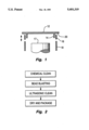
- FIG. 1 is a cross sectional view of a replaceable lid, door and shield for a vacuum processing chamber.
- FIG. 2 is a flow chart for the process of the invention.
- FIG. 1 illustrates the novel one piece aluminum lid of the invention, a quartz door therefor and a quartz substrate support shield for a vacuum processing chamber.
- the lid is opposed to the cathode within the chamber on which the substrate to be treated is placed during processing.
- the lid and door of the invention have been pre-treated in accordance with the process of the invention.
- the extension wall 14 fits inside a quartz door 16.
- the door 16 fits atop a quartz shield 18 which is shaped to surround the cathode 17 onto which the substrate to be processed is located during processing.
- the door 16 is raised and lowered with lid 12 stationary by an externally driven actuator.
- ceramic fingers (not shown), which pass through slots in the quartz shield 18, raise and lower the substrate onto the cathode 17. This occurs during the transfer of substrates into and out of the chamber.
- the fixed quartz shield 18 serves to prevent material etched from the substrate from adhering to the walls of the vacuum chamber (not shown).
- the lid 12 also has an overlying portion 20 of said first surface that contacts and seals the door during processing.
- a suitable O-ring seal (not shown) conventionally is used to seal the chamber when a vacuum is drawn.
- the aluminum lid 12 and the quartz door 16 and shield 18 are pre-treated in accordance with the cleaning process of the invention, described in greater detail hereinbelow.
- the novel lid of the invention requires no screws, thereby generating fewer particles in a vacuum preclean or processing chamber; has a pre-treated surface to which particles generated during processing better adhere; does not require an RF gasket, resulting in better grounding of the lid; and no assembly or disassembly of the lid is required for cleaning or replacement.
- a simple replacement of the lid and the door can be effected when required, reducing the downtime of the equipment.
- the lid, door and shield also can be readily re-cleaned and re-treated for reuse in any suitable vacuum chamber.
- Aluminum parts and quartz parts are recycle-cleaned by a combination of bead blasting and chemical cleaning steps. The last step in both cases is a bead blasting step followed by ultrasonic processing in deionized water, rinsing and drying as explained further hereinbelow.
- the pretreatment process of the invention comprises a bead blasting step followed by an ultrasonic cleaning step.
- the bead blasting step treatment of the aluminum lid and the quartz door is suitably effected by bombarding the lid, the door and the shield using about 80 psi of pressure and aluminum oxide powder having a rather coarse grit, suitably about 36-80 grit in size.
- Bead blasting can be carried out in commercially available bead blasting equipment.
- the bead blasting powder particles must be large enough to make the aluminum surface of the lid and the quartz door and shield surfaces slightly irregular or roughened.
- the machined one-piece aluminum lid can withstand bead blasting with coarser grit size material because it is thicker than the prior art two-plate aluminum sheet metal lid, and thus it is more durable.
- the irregular surfaces will enhance interface crack propagation of material that may be deposited during substrate processing.
- the surface irregularities will result in the breaking up of the deposited films into sections that are small with respect to flake sizes, which significantly hinders flaking.
- the irregular or roughened surfaces have an increased surface area to which material can deposit, increasing the amount of deposited material that can be accommodated.
- the bead blasting step is followed by an ultrasonic cleaning step that removes all loose particles on the surfaces of the lid, door and shield, whether they are due to particles remaining from the bead blasting, or minute particles of aluminum, quartz, dust particles and the like.
- the lid, door and shield are first rinsed with deionized water and immersed in an ultrasonic cleaner filled with deionized water.
- Suitable ultrasonic cleaners are commercially available and are generally set to run at power densities of from about 35-70 Watts/gallon using a chamber containing about 10 gallons of deionized water for several minutes. As soon as the ultrasonic generator is turned on, a cloud of formerly embedded solid residue is seen to form over the bead blasted surfaces from which it originated.
- the aluminum lid and quartz door and shield parts are dried to remove all moisture from their surfaces.
- the parts can be blown dry with filtered air or nitrogen and then lightly baked, e.g., at about 60° C. for one-half hour in filtered air atmosphere to remove all moisture from the parts.
- the cleaned parts can then be packed for shipment.
- the parts are chemically cleaned to remove surface contamination, such as oxides from the aluminum and organics from the quartz surfaces.
- a suitable chemical cleaning solution for ceramics for example can be 1/3 nitric acid, 1/3 hydrofluoric acid and 1/3 water. Dipping the part in the chemical cleaning solution for about 15 seconds is generally sufficient.
- the part is then rinsed with deionized water to remove the chemicals and blown dry using clean, filtered air or nitrogen.
- FIG. 2 is a flow chart of the preferred embodiment of the process of the invention, showing the chemical clean first step, followed by a bead blasting step, an ultrasonic cleaning step, and lastly the part finished by rinsing and drying and packaging the part.
- Treating the lid and quartz parts of the vacuum chamber in accordance with the process of the invention, and utilizing the simplified, sturdier lid of the present invention, results in a cleaner vacuum chamber, one that can process more substrates than prior art chamber, reducing downtime of the equipment, and also provides a fast and low cost method of cleaning the chambers, and replacing the above-described parts.
- semiconductor substrates are generally silicon wafers which are circular in cross section, resulting in shields and cathode supports that are also circular in cross section, other substrates such as rectangular glass plates can also be employed.
- Other materials can be substituted for aluminum, such as stainless steel; and other cleaning and rinsing steps inserted into the process for particular results.
- the invention is only meant to be limited by the appended claims.
Abstract
Replaceable parts for a vacuum chamber including an aluminum lid and a quartz door and shield, are treated to clean and roughen their surfaces to increase adhesion of materials deposited thereon during substrate processing in said chamber, thereby reducing downtime of the equipment. The parts can be chemically cleaned, rinsed to remove the chemicals and dried in a first step; subjected to bead blasting to roughen the surface of the part and improve adhesion thereon of deposited material; in a succeeding step the part to be cleaned ultrasonically in order to remove all loose particles; and in a last step the parts rinsed and dried to remove moisture, prior to packaging or using the part. A novel single-piece machined aluminum lid has an extension wall from a first surface that fits into the door of the chamber, and an overlying portion of said first surface that sealingly engages the door when the lid is closed.
Description
This invention relates to improved replaceable parts for a vacuum chamber. More particularly, this invention relates to replaceable parts for a vacuum etch chamber that are pretreated to extend the time for replacement.
Vacuum chambers are well known and are employed in the semiconductor industry to etch and deposit thin films and form contacts in semiconductor substrates during manufacture of, inter alia, integrated circuits. State-of-the art processing chambers form a part of a system able to condition and preclean substrates for vacuum processing and process them without leaving a vacuum environment.
However, a substrate preclean step, while it is effective in removing material adhered to the surface of the substrate, distributes this :material on other surfaces within the vacuum chamber, e.g., on the walls or shields, lid and door of the chamber. In time there is a build up of this material that causes flakes to form on these surfaces that can deposit onto the substrate surface. At that point the chamber must be disassembled for cleaning.
The present lid for a vacuum etch chamber comprises a two-piece aluminum lid separated by an RF gasket, which is a low resistance contact for the 60 MHz RF power supply for the vacuum chamber. Two aluminum plates are screwed together by a plurality of screws that fasten the two plates together so they make good contact to the RF gasket therebetween. As material builds up on the lid however, as described hereinabove, it must be periodically cleaned to remove the built up material. This is generally done by a wet chemical cleaning process which requires that the lid be disassembled, the screws removed, the lid cleaned and then the lid be re-assembled. However, the act of assembly, e.g., inserting and fastening the screws, itself creates particles, so that the chamber is not clean, i.e., free of particles, even after the cleaning step. Other parts of the vacuum chamber, such as the door for the lid and a shield around the substrate support that prevents material from depositing on the walls of the chamber, must also be periodically cleaned; this adds to the downtime of the equipment and consequently increases costs of manufacture.
Thus it would be desirable to have a vacuum chamber lid that does not have to be disassembled and assembled again for cleaning; further it would be desirable to pre-treat replaceable parts for a vacuum chamber so that particles generated in the vacuum chamber that adhere to the lid, door and shield surfaces have improved adherence to these surfaces with the result that the time between cleaning cycles can be extended, thereby reducing downtime of the equipment.
The present invention provides a novel lid and door for a vacuum chamber comprising a single, machined aluminum plate that sealingly engages a quartz ring or door, and, when the lid and door to the vacuum chamber are closed, in turn fits inside a shield surrounding the substrate support. The lid, shield and door replaceable parts are pre-treated so that particles generated within the chamber during precleaning of the substrate and processing thereof will better adhere to these surfaces, allowing more substrates to be processed before the vacuum chamber needs to be taken apart and cleaned or parts replaced. This pre-treatment comprises a bead blasting step that creates an irregular surface in the aluminum and quartz materials of the replaceable parts, e.g., lid, door and shield respectively, to which materials or particles generated in the chamber adhere better than on a smooth surface, followed by removal of all particles remaining on the surface after the bead blasting step by an ultrasonic cleaning step of the replaceable parts. This pre-treatment produces aluminum and quartz door/lid/shield combinations that have a long lifetime in a vacuum processing chamber.
FIG. 1 is a cross sectional view of a replaceable lid, door and shield for a vacuum processing chamber.
FIG. 2 is a flow chart for the process of the invention.
FIG. 1 illustrates the novel one piece aluminum lid of the invention, a quartz door therefor and a quartz substrate support shield for a vacuum processing chamber. The lid is opposed to the cathode within the chamber on which the substrate to be treated is placed during processing. The lid and door of the invention have been pre-treated in accordance with the process of the invention.
The extension wall 14 fits inside a quartz door 16. When the lid 14 is in place and the door 16 is closed, the door 16 fits atop a quartz shield 18 which is shaped to surround the cathode 17 onto which the substrate to be processed is located during processing. The door 16 is raised and lowered with lid 12 stationary by an externally driven actuator. At the same time the door 16 is raised and lowered, ceramic fingers (not shown), which pass through slots in the quartz shield 18, raise and lower the substrate onto the cathode 17. This occurs during the transfer of substrates into and out of the chamber. The fixed quartz shield 18 serves to prevent material etched from the substrate from adhering to the walls of the vacuum chamber (not shown). The lid 12 also has an overlying portion 20 of said first surface that contacts and seals the door during processing. A suitable O-ring seal (not shown) conventionally is used to seal the chamber when a vacuum is drawn.
The aluminum lid 12 and the quartz door 16 and shield 18 are pre-treated in accordance with the cleaning process of the invention, described in greater detail hereinbelow.
The novel lid of the invention requires no screws, thereby generating fewer particles in a vacuum preclean or processing chamber; has a pre-treated surface to which particles generated during processing better adhere; does not require an RF gasket, resulting in better grounding of the lid; and no assembly or disassembly of the lid is required for cleaning or replacement. A simple replacement of the lid and the door can be effected when required, reducing the downtime of the equipment. The lid, door and shield also can be readily re-cleaned and re-treated for reuse in any suitable vacuum chamber. Aluminum parts and quartz parts are recycle-cleaned by a combination of bead blasting and chemical cleaning steps. The last step in both cases is a bead blasting step followed by ultrasonic processing in deionized water, rinsing and drying as explained further hereinbelow.
The pretreatment process of the invention comprises a bead blasting step followed by an ultrasonic cleaning step.
The bead blasting step treatment of the aluminum lid and the quartz door is suitably effected by bombarding the lid, the door and the shield using about 80 psi of pressure and aluminum oxide powder having a rather coarse grit, suitably about 36-80 grit in size. Bead blasting can be carried out in commercially available bead blasting equipment. The bead blasting powder particles must be large enough to make the aluminum surface of the lid and the quartz door and shield surfaces slightly irregular or roughened. The machined one-piece aluminum lid can withstand bead blasting with coarser grit size material because it is thicker than the prior art two-plate aluminum sheet metal lid, and thus it is more durable. The irregular surfaces, on a microscopic scale, will enhance interface crack propagation of material that may be deposited during substrate processing. The surface irregularities will result in the breaking up of the deposited films into sections that are small with respect to flake sizes, which significantly hinders flaking. In addition, the irregular or roughened surfaces have an increased surface area to which material can deposit, increasing the amount of deposited material that can be accommodated.
The bead blasting step is followed by an ultrasonic cleaning step that removes all loose particles on the surfaces of the lid, door and shield, whether they are due to particles remaining from the bead blasting, or minute particles of aluminum, quartz, dust particles and the like. The lid, door and shield are first rinsed with deionized water and immersed in an ultrasonic cleaner filled with deionized water. Suitable ultrasonic cleaners are commercially available and are generally set to run at power densities of from about 35-70 Watts/gallon using a chamber containing about 10 gallons of deionized water for several minutes. As soon as the ultrasonic generator is turned on, a cloud of formerly embedded solid residue is seen to form over the bead blasted surfaces from which it originated. This cloud quickly dissipates and the solid material removed either remains in aqueous suspension or settles out. Thus, most of the activity of ultrasonic processing occurs during the initial few seconds of treatment. Treatment is usually continued for about 5 minutes however, in order to assure thorough removal of all loose solid material. The parts are then thoroughly rinsed with hot deionized water to ensure that no particles remain on the surfaces of the treated aluminum and quartz parts.
Lastly, the aluminum lid and quartz door and shield parts are dried to remove all moisture from their surfaces. Suitably the parts can be blown dry with filtered air or nitrogen and then lightly baked, e.g., at about 60° C. for one-half hour in filtered air atmosphere to remove all moisture from the parts. The cleaned parts can then be packed for shipment.
In a preferred cleaning process, prior to the bead blasting step the parts are chemically cleaned to remove surface contamination, such as oxides from the aluminum and organics from the quartz surfaces. A suitable chemical cleaning solution for ceramics for example can be 1/3 nitric acid, 1/3 hydrofluoric acid and 1/3 water. Dipping the part in the chemical cleaning solution for about 15 seconds is generally sufficient. The part is then rinsed with deionized water to remove the chemicals and blown dry using clean, filtered air or nitrogen.
FIG. 2 is a flow chart of the preferred embodiment of the process of the invention, showing the chemical clean first step, followed by a bead blasting step, an ultrasonic cleaning step, and lastly the part finished by rinsing and drying and packaging the part.
Treating the lid and quartz parts of the vacuum chamber in accordance with the process of the invention, and utilizing the simplified, sturdier lid of the present invention, results in a cleaner vacuum chamber, one that can process more substrates than prior art chamber, reducing downtime of the equipment, and also provides a fast and low cost method of cleaning the chambers, and replacing the above-described parts.
Although the above invention has been described in terms of certain presently preferred embodiments, one skilled in the art will know of alternative embodiments of processing and equipment which are meant to be included herein. For example, although semiconductor substrates are generally silicon wafers which are circular in cross section, resulting in shields and cathode supports that are also circular in cross section, other substrates such as rectangular glass plates can also be employed. Other materials can be substituted for aluminum, such as stainless steel; and other cleaning and rinsing steps inserted into the process for particular results. The invention is only meant to be limited by the appended claims.
Claims (4)
1. A process for treating component parts for a vacuum etch chamber, said parts made of a material selected from the group consisting of aluminum and ceramic, comprising the steps in sequence:
a) bead blasting the surface of the part to roughen the surface;
b) ultrasonically cleaning the part to remove surface particles; and
c) rinsing and drying the part.
2. A process according to claim 1 wherein the parts are first cleaned with a chemical cleaning solution.
3. A process according to claim 1 wherein one of the parts is an aluminum single-piece lid for the vacuum chamber.
4. A process according to claim 1 wherein one or more parts are made of quartz.
Priority Applications (7)
| Application Number | Priority Date | Filing Date | Title |
|---|---|---|---|
| US07/936,433 US5401319A (en) | 1992-08-27 | 1992-08-27 | Lid and door for a vacuum chamber and pretreatment therefor |
| JP5190301A JP2568371B2 (en) | 1992-08-27 | 1993-07-30 | Novel lid and door for vacuum chamber and pretreatment |
| KR1019930016654A KR100271190B1 (en) | 1992-08-27 | 1993-08-26 | Vacuum erosion chamber |
| EP93113770A EP0589237B1 (en) | 1992-08-27 | 1993-08-27 | Vacuum etch chamber and method for treating parts thereof |
| DE69322043T DE69322043T2 (en) | 1992-08-27 | 1993-08-27 | Vacuum etching chamber and method for treating its parts |
| US08/335,611 US5565058A (en) | 1992-08-27 | 1994-11-08 | Lid and door for a vacuum chamber and pretreatment therefor |
| US08/658,784 US5762748A (en) | 1992-08-27 | 1996-06-05 | Lid and door for a vacuum chamber and pretreatment therefor |
Applications Claiming Priority (1)
| Application Number | Priority Date | Filing Date | Title |
|---|---|---|---|
| US07/936,433 US5401319A (en) | 1992-08-27 | 1992-08-27 | Lid and door for a vacuum chamber and pretreatment therefor |
Related Child Applications (1)
| Application Number | Title | Priority Date | Filing Date |
|---|---|---|---|
| US08/335,611 Division US5565058A (en) | 1992-08-27 | 1994-11-08 | Lid and door for a vacuum chamber and pretreatment therefor |
Publications (1)
| Publication Number | Publication Date |
|---|---|
| US5401319A true US5401319A (en) | 1995-03-28 |
Family
ID=25468625
Family Applications (3)
| Application Number | Title | Priority Date | Filing Date |
|---|---|---|---|
| US07/936,433 Expired - Fee Related US5401319A (en) | 1992-08-27 | 1992-08-27 | Lid and door for a vacuum chamber and pretreatment therefor |
| US08/335,611 Expired - Fee Related US5565058A (en) | 1992-08-27 | 1994-11-08 | Lid and door for a vacuum chamber and pretreatment therefor |
| US08/658,784 Expired - Lifetime US5762748A (en) | 1992-08-27 | 1996-06-05 | Lid and door for a vacuum chamber and pretreatment therefor |
Family Applications After (2)
| Application Number | Title | Priority Date | Filing Date |
|---|---|---|---|
| US08/335,611 Expired - Fee Related US5565058A (en) | 1992-08-27 | 1994-11-08 | Lid and door for a vacuum chamber and pretreatment therefor |
| US08/658,784 Expired - Lifetime US5762748A (en) | 1992-08-27 | 1996-06-05 | Lid and door for a vacuum chamber and pretreatment therefor |
Country Status (5)
| Country | Link |
|---|---|
| US (3) | US5401319A (en) |
| EP (1) | EP0589237B1 (en) |
| JP (1) | JP2568371B2 (en) |
| KR (1) | KR100271190B1 (en) |
| DE (1) | DE69322043T2 (en) |
Cited By (33)
| Publication number | Priority date | Publication date | Assignee | Title |
|---|---|---|---|---|
| US5916454A (en) * | 1996-08-30 | 1999-06-29 | Lam Research Corporation | Methods and apparatus for reducing byproduct particle generation in a plasma processing chamber |
| US6036780A (en) * | 1997-08-27 | 2000-03-14 | Cypress Semiconductor Corporation | Mechanism for detecting particulate formation and/or failures in the removal of gas from a liquid |
| US6105435A (en) * | 1997-10-24 | 2000-08-22 | Cypress Semiconductor Corp. | Circuit and apparatus for verifying a chamber seal, and method of depositing a material onto a substrate using the same |
| US6368410B1 (en) | 1999-06-28 | 2002-04-09 | General Electric Company | Semiconductor processing article |
| US20020173117A1 (en) * | 1999-06-28 | 2002-11-21 | Gorczyca Thomas Bert | Semiconductor processing component |
| US20030172952A1 (en) * | 2002-03-18 | 2003-09-18 | Tokyo Electron Limited | Method of cleaning a plasma processing apparatus |
| US20030185965A1 (en) * | 2002-03-27 | 2003-10-02 | Applied Materials, Inc. | Evaluation of chamber components having textured coatings |
| US20040056211A1 (en) * | 2002-03-13 | 2004-03-25 | Applied Materials, Inc. | Method of surface texturizing |
| US20040099285A1 (en) * | 2002-11-25 | 2004-05-27 | Applied Materials, Inc. | Method of cleaning a coated process chamber component |
| US6805952B2 (en) | 2000-12-29 | 2004-10-19 | Lam Research Corporation | Low contamination plasma chamber components and methods for making the same |
| US20050048876A1 (en) * | 2003-09-02 | 2005-03-03 | Applied Materials, Inc. | Fabricating and cleaning chamber components having textured surfaces |
| US20050089699A1 (en) * | 2003-10-22 | 2005-04-28 | Applied Materials, Inc. | Cleaning and refurbishing chamber components having metal coatings |
| US20050172984A1 (en) * | 2004-02-11 | 2005-08-11 | Applied Materials, Inc. | Cleaning of chamber components |
| US20050238807A1 (en) * | 2004-04-27 | 2005-10-27 | Applied Materials, Inc. | Refurbishment of a coated chamber component |
| US20050271984A1 (en) * | 2004-06-07 | 2005-12-08 | Applied Materials, Inc. | Textured chamber surface |
| US20060105182A1 (en) * | 2004-11-16 | 2006-05-18 | Applied Materials, Inc. | Erosion resistant textured chamber surface |
| US20060110620A1 (en) * | 2004-11-24 | 2006-05-25 | Applied Materials, Inc. | Process chamber component with layered coating and method |
| US20070059460A1 (en) * | 2005-09-09 | 2007-03-15 | Applied Materials, Inc. | Flow-formed chamber component having a textured surface |
| US20070102286A1 (en) * | 2005-10-31 | 2007-05-10 | Applied Materials, Inc. | Process kit and target for substrate processing chamber |
| US20070113783A1 (en) * | 2005-11-19 | 2007-05-24 | Applied Materials, Inc. | Band shield for substrate processing chamber |
| US20070173059A1 (en) * | 2005-11-25 | 2007-07-26 | Applied Materials, Inc. | Process kit components for titanium sputtering chamber |
| US20070283884A1 (en) * | 2006-05-30 | 2007-12-13 | Applied Materials, Inc. | Ring assembly for substrate processing chamber |
| US20080295872A1 (en) * | 2007-05-30 | 2008-12-04 | Applied Materials, Inc. | Substrate cleaning chamber and components |
| US20090084317A1 (en) * | 2007-09-28 | 2009-04-02 | Applied Materials, Inc. | Atomic layer deposition chamber and components |
| US20090194414A1 (en) * | 2008-01-31 | 2009-08-06 | Nolander Ira G | Modified sputtering target and deposition components, methods of production and uses thereof |
| US7670436B2 (en) | 2004-11-03 | 2010-03-02 | Applied Materials, Inc. | Support ring assembly |
| US7964085B1 (en) | 2002-11-25 | 2011-06-21 | Applied Materials, Inc. | Electrochemical removal of tantalum-containing materials |
| US7981262B2 (en) | 2007-01-29 | 2011-07-19 | Applied Materials, Inc. | Process kit for substrate processing chamber |
| US8617672B2 (en) | 2005-07-13 | 2013-12-31 | Applied Materials, Inc. | Localized surface annealing of components for substrate processing chambers |
| US20140190937A1 (en) * | 2000-08-11 | 2014-07-10 | Quantum Global Technologies LLC | System and Method for Cleaning Semiconductor Fabrication Equipment Parts |
| US9101954B2 (en) | 2013-09-17 | 2015-08-11 | Applied Materials, Inc. | Geometries and patterns for surface texturing to increase deposition retention |
| US11139151B1 (en) * | 2018-03-15 | 2021-10-05 | Intel Corporation | Micro-surface morphological matching for reactor components |
| CN114102440A (en) * | 2020-08-28 | 2022-03-01 | 长鑫存储技术有限公司 | Surface treatment method for quartz member |
Families Citing this family (35)
| Publication number | Priority date | Publication date | Assignee | Title |
|---|---|---|---|---|
| US6007673A (en) * | 1996-10-02 | 1999-12-28 | Matsushita Electronics Corporation | Apparatus and method of producing an electronic device |
| US5945354A (en) * | 1997-02-03 | 1999-08-31 | Motorola, Inc. | Method for reducing particles deposited onto a semiconductor wafer during plasma processing |
| US6168696B1 (en) | 1999-09-01 | 2001-01-02 | Micron Technology, Inc. | Non-knurled induction coil for ionized metal deposition, sputtering apparatus including same, and method of constructing the apparatus |
| JP4294176B2 (en) * | 1999-09-13 | 2009-07-08 | 株式会社山形信越石英 | Method for cleaning quartz articles with a grained surface |
| US20020069970A1 (en) * | 2000-03-07 | 2002-06-13 | Applied Materials, Inc. | Temperature controlled semiconductor processing chamber liner |
| US6777045B2 (en) * | 2001-06-27 | 2004-08-17 | Applied Materials Inc. | Chamber components having textured surfaces and method of manufacture |
| US20030047464A1 (en) * | 2001-07-27 | 2003-03-13 | Applied Materials, Inc. | Electrochemically roughened aluminum semiconductor processing apparatus surfaces |
| US6587750B2 (en) | 2001-09-25 | 2003-07-01 | Intuitive Surgical, Inc. | Removable infinite roll master grip handle and touch sensor for robotic surgery |
| KR100439478B1 (en) * | 2001-12-22 | 2004-07-09 | 동부전자 주식회사 | Method for cleaning a shield of a metal film deposition apparatus |
| US6776873B1 (en) * | 2002-02-14 | 2004-08-17 | Jennifer Y Sun | Yttrium oxide based surface coating for semiconductor IC processing vacuum chambers |
| US20060086320A1 (en) * | 2002-05-24 | 2006-04-27 | Michael Lizenberg | Method and device for plasma treating workpieces |
| DE10224547B4 (en) * | 2002-05-24 | 2020-06-25 | Khs Corpoplast Gmbh | Method and device for the plasma treatment of workpieces |
| WO2004012242A1 (en) * | 2002-07-26 | 2004-02-05 | Applied Materials, Inc. | Hydrophilic components for a spin-rinse-dryer |
| US20040221959A1 (en) * | 2003-05-09 | 2004-11-11 | Applied Materials, Inc. | Anodized substrate support |
| US7045072B2 (en) * | 2003-07-24 | 2006-05-16 | Tan Samantha S H | Cleaning process and apparatus for silicate materials |
| US20070012658A1 (en) * | 2003-09-25 | 2007-01-18 | Mize John D | Pvd component and coil refurbishing methods |
| US7416076B2 (en) * | 2004-01-12 | 2008-08-26 | Halliburton Energy Services, Inc. | Apparatus and method for packaging and shipping of high explosive content components |
| US20050211276A1 (en) * | 2004-03-15 | 2005-09-29 | Applied Materials, Inc. | Lid for a semiconductor device processing apparatus and methods for using the same |
| US7648582B2 (en) * | 2005-12-23 | 2010-01-19 | Lam Research Corporation | Cleaning of electrostatic chucks using ultrasonic agitation and applied electric fields |
| US8173228B2 (en) * | 2006-01-27 | 2012-05-08 | Applied Materials, Inc. | Particle reduction on surfaces of chemical vapor deposition processing apparatus |
| DE102006026828A1 (en) * | 2006-06-07 | 2007-12-13 | Hydro Aluminium Deutschland Gmbh | Method for producing a container from aluminum sheets |
| US8444926B2 (en) * | 2007-01-30 | 2013-05-21 | Applied Materials, Inc. | Processing chamber with heated chamber liner |
| US20080196661A1 (en) * | 2007-02-20 | 2008-08-21 | Brian West | Plasma sprayed deposition ring isolator |
| US7741583B2 (en) * | 2007-03-22 | 2010-06-22 | Tokyo Electron Limited | Bake plate lid cleaner and cleaning method |
| US10242888B2 (en) | 2007-04-27 | 2019-03-26 | Applied Materials, Inc. | Semiconductor processing apparatus with a ceramic-comprising surface which exhibits fracture toughness and halogen plasma resistance |
| US10622194B2 (en) | 2007-04-27 | 2020-04-14 | Applied Materials, Inc. | Bulk sintered solid solution ceramic which exhibits fracture toughness and halogen plasma resistance |
| JP4669017B2 (en) * | 2008-02-29 | 2011-04-13 | 富士フイルム株式会社 | Film forming apparatus, gas barrier film, and gas barrier film manufacturing method |
| US20090261065A1 (en) * | 2008-04-18 | 2009-10-22 | Lam Research Corporation | Components for use in a plasma chamber having reduced particle generation and method of making |
| TWI502617B (en) * | 2010-07-21 | 2015-10-01 | 應用材料股份有限公司 | Method,plasma processing apparatus ,and liner assembly for tuning electrical skews |
| US9713552B2 (en) | 2010-09-09 | 2017-07-25 | Zuiko Corporation | Method and apparatus for producing wearing article, and wearing article |
| CN102513305B (en) * | 2011-12-30 | 2016-03-02 | 上海集成电路研发中心有限公司 | The cleaning device of semi-conductor silicon chip and cleaning method thereof |
| CN103510064B (en) * | 2012-06-15 | 2016-06-29 | 中微半导体设备(上海)有限公司 | Vacuum treatment installation and the method controlling processing procedure granule deposition path |
| USD913979S1 (en) | 2019-08-28 | 2021-03-23 | Applied Materials, Inc. | Inner shield for a substrate processing chamber |
| US11534967B2 (en) | 2019-12-12 | 2022-12-27 | Arcam Ab | Additive manufacturing apparatuses with powder distributors and methods of use |
| USD973609S1 (en) | 2020-04-22 | 2022-12-27 | Applied Materials, Inc. | Upper shield with showerhead for a process chamber |
Citations (5)
| Publication number | Priority date | Publication date | Assignee | Title |
|---|---|---|---|---|
| JPS60100657A (en) * | 1983-11-08 | 1985-06-04 | Toshiba Corp | Surface treatment of metal |
| US5017439A (en) * | 1989-07-19 | 1991-05-21 | Seagate Technology, Inc. | Micro-contamination-free coating for die-cast component in magnetic disk drive |
| EP0446657A1 (en) * | 1990-03-02 | 1991-09-18 | Applied Materials, Inc. | Method for preparing a shield to reduce particles in a physical vapor deposition chamber |
| US5051375A (en) * | 1988-07-11 | 1991-09-24 | Kyushu Electronic Metal Co., Ltd. | Method of producing semiconductor wafer through gettering using spherical abrasives |
| US5202008A (en) * | 1990-03-02 | 1993-04-13 | Applied Materials, Inc. | Method for preparing a shield to reduce particles in a physical vapor deposition chamber |
Family Cites Families (11)
| Publication number | Priority date | Publication date | Assignee | Title |
|---|---|---|---|---|
| US3617463A (en) * | 1969-06-18 | 1971-11-02 | Ibm | Apparatus and method for sputter etching |
| SE425707B (en) * | 1981-03-20 | 1982-10-25 | Asea Ab | WAY TO INCLUDE BURNING NUCLEAR FUEL RODS IN A COPPER CONTAINER |
| US4411575A (en) * | 1981-05-01 | 1983-10-25 | The Perkin-Elmer Corporation | Sample transfer vessel |
| US4466872A (en) * | 1982-12-23 | 1984-08-21 | At&T Technologies, Inc. | Methods of and apparatus for depositing a continuous film of minimum thickness |
| US4657616A (en) * | 1985-05-17 | 1987-04-14 | Benzing Technologies, Inc. | In-situ CVD chamber cleaner |
| JP2859632B2 (en) * | 1988-04-14 | 1999-02-17 | キヤノン株式会社 | Film forming apparatus and film forming method |
| US5233144A (en) * | 1988-06-14 | 1993-08-03 | Sharp Kabushiki Kaisha | Heat generating container for microwave oven |
| JPH03180500A (en) * | 1989-12-07 | 1991-08-06 | Fujitsu Ltd | Method for treating surface of inner wall of stainless-steel vacuum vessel |
| DE69129081T2 (en) * | 1990-01-29 | 1998-07-02 | Varian Associates | Device and method for precipitation by a collimator |
| JP3471032B2 (en) * | 1991-12-27 | 2003-11-25 | アネルバ株式会社 | Thin film deposition equipment |
| JPH05247635A (en) * | 1992-03-05 | 1993-09-24 | Fujitsu Ltd | Sputtering device |
-
1992
- 1992-08-27 US US07/936,433 patent/US5401319A/en not_active Expired - Fee Related
-
1993
- 1993-07-30 JP JP5190301A patent/JP2568371B2/en not_active Expired - Fee Related
- 1993-08-26 KR KR1019930016654A patent/KR100271190B1/en not_active IP Right Cessation
- 1993-08-27 DE DE69322043T patent/DE69322043T2/en not_active Expired - Fee Related
- 1993-08-27 EP EP93113770A patent/EP0589237B1/en not_active Expired - Lifetime
-
1994
- 1994-11-08 US US08/335,611 patent/US5565058A/en not_active Expired - Fee Related
-
1996
- 1996-06-05 US US08/658,784 patent/US5762748A/en not_active Expired - Lifetime
Patent Citations (5)
| Publication number | Priority date | Publication date | Assignee | Title |
|---|---|---|---|---|
| JPS60100657A (en) * | 1983-11-08 | 1985-06-04 | Toshiba Corp | Surface treatment of metal |
| US5051375A (en) * | 1988-07-11 | 1991-09-24 | Kyushu Electronic Metal Co., Ltd. | Method of producing semiconductor wafer through gettering using spherical abrasives |
| US5017439A (en) * | 1989-07-19 | 1991-05-21 | Seagate Technology, Inc. | Micro-contamination-free coating for die-cast component in magnetic disk drive |
| EP0446657A1 (en) * | 1990-03-02 | 1991-09-18 | Applied Materials, Inc. | Method for preparing a shield to reduce particles in a physical vapor deposition chamber |
| US5202008A (en) * | 1990-03-02 | 1993-04-13 | Applied Materials, Inc. | Method for preparing a shield to reduce particles in a physical vapor deposition chamber |
Non-Patent Citations (4)
| Title |
|---|
| Lee et al, "adhesion studies . . . " 2194 Thin Solid Films 185 (1990) Feb., No. 12 Lausanne, CH pp. 35-55. |
| Lee et al, adhesion studies . . . 2194 Thin Solid Films 185 (1990) Feb., No. 12 Lausanne, CH pp. 35 55. * |
| Search Report EP (1993). * |
| Search Report-EP (1993). |
Cited By (69)
| Publication number | Priority date | Publication date | Assignee | Title |
|---|---|---|---|---|
| US5916454A (en) * | 1996-08-30 | 1999-06-29 | Lam Research Corporation | Methods and apparatus for reducing byproduct particle generation in a plasma processing chamber |
| US6036780A (en) * | 1997-08-27 | 2000-03-14 | Cypress Semiconductor Corporation | Mechanism for detecting particulate formation and/or failures in the removal of gas from a liquid |
| US6494100B1 (en) | 1997-10-24 | 2002-12-17 | Cypress Semiconductor Corp. | Circuit and apparatus for verifying a chamber seal, and method of depositing a material onto a substrate using the same |
| US6105435A (en) * | 1997-10-24 | 2000-08-22 | Cypress Semiconductor Corp. | Circuit and apparatus for verifying a chamber seal, and method of depositing a material onto a substrate using the same |
| US6368410B1 (en) | 1999-06-28 | 2002-04-09 | General Electric Company | Semiconductor processing article |
| US20020173117A1 (en) * | 1999-06-28 | 2002-11-21 | Gorczyca Thomas Bert | Semiconductor processing component |
| US20020094686A1 (en) * | 1999-06-28 | 2002-07-18 | Gorczyca Thomas Bert | Semiconductor processing article |
| US6504233B1 (en) | 1999-06-28 | 2003-01-07 | General Electric Company | Semiconductor processing component |
| US6706205B2 (en) * | 1999-06-28 | 2004-03-16 | General Electric Company | Semiconductor processing article |
| US6709608B2 (en) | 1999-06-28 | 2004-03-23 | General Electric Company | Semiconductor processing component |
| US20140190937A1 (en) * | 2000-08-11 | 2014-07-10 | Quantum Global Technologies LLC | System and Method for Cleaning Semiconductor Fabrication Equipment Parts |
| US6805952B2 (en) | 2000-12-29 | 2004-10-19 | Lam Research Corporation | Low contamination plasma chamber components and methods for making the same |
| US20040224128A1 (en) * | 2000-12-29 | 2004-11-11 | Lam Research Corporation | Low contamination plasma chamber components and methods for making the same |
| US20040056211A1 (en) * | 2002-03-13 | 2004-03-25 | Applied Materials, Inc. | Method of surface texturizing |
| US6812471B2 (en) * | 2002-03-13 | 2004-11-02 | Applied Materials, Inc. | Method of surface texturizing |
| US6790289B2 (en) * | 2002-03-18 | 2004-09-14 | Tokyo Electric Limited | Method of cleaning a plasma processing apparatus |
| US20040216769A1 (en) * | 2002-03-18 | 2004-11-04 | Tokyo Electron Limited | Method of cleaning a plasma processing apparatus |
| US20030172952A1 (en) * | 2002-03-18 | 2003-09-18 | Tokyo Electron Limited | Method of cleaning a plasma processing apparatus |
| US7026009B2 (en) | 2002-03-27 | 2006-04-11 | Applied Materials, Inc. | Evaluation of chamber components having textured coatings |
| US20030185965A1 (en) * | 2002-03-27 | 2003-10-02 | Applied Materials, Inc. | Evaluation of chamber components having textured coatings |
| US20040163669A1 (en) * | 2002-11-25 | 2004-08-26 | Applied Materials, Inc. | Cleaning chamber surfaces to recover metal-containing compounds |
| US20040099285A1 (en) * | 2002-11-25 | 2004-05-27 | Applied Materials, Inc. | Method of cleaning a coated process chamber component |
| US9068273B2 (en) | 2002-11-25 | 2015-06-30 | Quantum Global Technologies LLC | Electrochemical removal of tantalum-containing materials |
| US6902628B2 (en) | 2002-11-25 | 2005-06-07 | Applied Materials, Inc. | Method of cleaning a coated process chamber component |
| US6902627B2 (en) | 2002-11-25 | 2005-06-07 | Applied Materials, Inc. | Cleaning chamber surfaces to recover metal-containing compounds |
| US7964085B1 (en) | 2002-11-25 | 2011-06-21 | Applied Materials, Inc. | Electrochemical removal of tantalum-containing materials |
| US7993470B2 (en) | 2003-09-02 | 2011-08-09 | Applied Materials, Inc. | Fabricating and cleaning chamber components having textured surfaces |
| US20080038481A1 (en) * | 2003-09-02 | 2008-02-14 | Applied Materials, Inc. | Fabricating and cleaning chamber components having textured surfaces |
| US20050048876A1 (en) * | 2003-09-02 | 2005-03-03 | Applied Materials, Inc. | Fabricating and cleaning chamber components having textured surfaces |
| US20090120462A1 (en) * | 2003-09-02 | 2009-05-14 | Applied Materials, Inc. | Fabricating and cleaning chamber components having textured surfaces |
| US20050089699A1 (en) * | 2003-10-22 | 2005-04-28 | Applied Materials, Inc. | Cleaning and refurbishing chamber components having metal coatings |
| US7910218B2 (en) | 2003-10-22 | 2011-03-22 | Applied Materials, Inc. | Cleaning and refurbishing chamber components having metal coatings |
| US20050172984A1 (en) * | 2004-02-11 | 2005-08-11 | Applied Materials, Inc. | Cleaning of chamber components |
| US7264679B2 (en) | 2004-02-11 | 2007-09-04 | Applied Materials, Inc. | Cleaning of chamber components |
| US20050238807A1 (en) * | 2004-04-27 | 2005-10-27 | Applied Materials, Inc. | Refurbishment of a coated chamber component |
| US20050271984A1 (en) * | 2004-06-07 | 2005-12-08 | Applied Materials, Inc. | Textured chamber surface |
| US8142989B2 (en) | 2004-06-07 | 2012-03-27 | Quantum Global Technologies LLC | Textured chamber surface |
| US20100059366A1 (en) * | 2004-06-07 | 2010-03-11 | Applied Materials, Inc. | Textured chamber surface |
| US7618769B2 (en) | 2004-06-07 | 2009-11-17 | Applied Materials, Inc. | Textured chamber surface |
| US7670436B2 (en) | 2004-11-03 | 2010-03-02 | Applied Materials, Inc. | Support ring assembly |
| US20060105182A1 (en) * | 2004-11-16 | 2006-05-18 | Applied Materials, Inc. | Erosion resistant textured chamber surface |
| US7579067B2 (en) | 2004-11-24 | 2009-08-25 | Applied Materials, Inc. | Process chamber component with layered coating and method |
| US8021743B2 (en) | 2004-11-24 | 2011-09-20 | Applied Materials, Inc. | Process chamber component with layered coating and method |
| US20100086805A1 (en) * | 2004-11-24 | 2010-04-08 | Applied Materials, Inc. | Process chamber component with layered coating and method |
| US20060110620A1 (en) * | 2004-11-24 | 2006-05-25 | Applied Materials, Inc. | Process chamber component with layered coating and method |
| US8617672B2 (en) | 2005-07-13 | 2013-12-31 | Applied Materials, Inc. | Localized surface annealing of components for substrate processing chambers |
| US9481608B2 (en) | 2005-07-13 | 2016-11-01 | Applied Materials, Inc. | Surface annealing of components for substrate processing chambers |
| US20070059460A1 (en) * | 2005-09-09 | 2007-03-15 | Applied Materials, Inc. | Flow-formed chamber component having a textured surface |
| US7762114B2 (en) | 2005-09-09 | 2010-07-27 | Applied Materials, Inc. | Flow-formed chamber component having a textured surface |
| US20070102286A1 (en) * | 2005-10-31 | 2007-05-10 | Applied Materials, Inc. | Process kit and target for substrate processing chamber |
| US10347475B2 (en) | 2005-10-31 | 2019-07-09 | Applied Materials, Inc. | Holding assembly for substrate processing chamber |
| US11658016B2 (en) | 2005-10-31 | 2023-05-23 | Applied Materials, Inc. | Shield for a substrate processing chamber |
| US9127362B2 (en) | 2005-10-31 | 2015-09-08 | Applied Materials, Inc. | Process kit and target for substrate processing chamber |
| US20070113783A1 (en) * | 2005-11-19 | 2007-05-24 | Applied Materials, Inc. | Band shield for substrate processing chamber |
| US8790499B2 (en) | 2005-11-25 | 2014-07-29 | Applied Materials, Inc. | Process kit components for titanium sputtering chamber |
| US20070173059A1 (en) * | 2005-11-25 | 2007-07-26 | Applied Materials, Inc. | Process kit components for titanium sputtering chamber |
| US20100065216A1 (en) * | 2006-05-30 | 2010-03-18 | Applied Materials, Inc. | Ring assembly for substrate processing chamber |
| US20070283884A1 (en) * | 2006-05-30 | 2007-12-13 | Applied Materials, Inc. | Ring assembly for substrate processing chamber |
| US7981262B2 (en) | 2007-01-29 | 2011-07-19 | Applied Materials, Inc. | Process kit for substrate processing chamber |
| US20080295872A1 (en) * | 2007-05-30 | 2008-12-04 | Applied Materials, Inc. | Substrate cleaning chamber and components |
| US7942969B2 (en) | 2007-05-30 | 2011-05-17 | Applied Materials, Inc. | Substrate cleaning chamber and components |
| US8980045B2 (en) | 2007-05-30 | 2015-03-17 | Applied Materials, Inc. | Substrate cleaning chamber and components |
| US20090084317A1 (en) * | 2007-09-28 | 2009-04-02 | Applied Materials, Inc. | Atomic layer deposition chamber and components |
| US20090194414A1 (en) * | 2008-01-31 | 2009-08-06 | Nolander Ira G | Modified sputtering target and deposition components, methods of production and uses thereof |
| US9101954B2 (en) | 2013-09-17 | 2015-08-11 | Applied Materials, Inc. | Geometries and patterns for surface texturing to increase deposition retention |
| US11139151B1 (en) * | 2018-03-15 | 2021-10-05 | Intel Corporation | Micro-surface morphological matching for reactor components |
| US20220028668A1 (en) * | 2018-03-15 | 2022-01-27 | Intel Corporation | Micro-surface morphological matching for reactor components |
| US11901164B2 (en) * | 2018-03-15 | 2024-02-13 | Intel Corporation | Micro-surface morphological matching for reactor components |
| CN114102440A (en) * | 2020-08-28 | 2022-03-01 | 长鑫存储技术有限公司 | Surface treatment method for quartz member |
Also Published As
| Publication number | Publication date |
|---|---|
| DE69322043D1 (en) | 1998-12-17 |
| JPH0817792A (en) | 1996-01-19 |
| EP0589237B1 (en) | 1998-11-11 |
| KR100271190B1 (en) | 2000-12-01 |
| KR940004741A (en) | 1994-03-15 |
| EP0589237A2 (en) | 1994-03-30 |
| JP2568371B2 (en) | 1997-01-08 |
| US5762748A (en) | 1998-06-09 |
| US5565058A (en) | 1996-10-15 |
| EP0589237A3 (en) | 1995-05-24 |
| DE69322043T2 (en) | 1999-06-24 |
Similar Documents
| Publication | Publication Date | Title |
|---|---|---|
| US5401319A (en) | Lid and door for a vacuum chamber and pretreatment therefor | |
| US5391275A (en) | Method for preparing a shield to reduce particles in a physical vapor deposition chamber | |
| US4576698A (en) | Plasma etch cleaning in low pressure chemical vapor deposition systems | |
| JP2674488B2 (en) | Dry etching chamber cleaning method | |
| TW369676B (en) | Electronic device producing apparatus and process for the same | |
| US20030185997A1 (en) | Method of reducing the chamber particle level | |
| EP0711455A1 (en) | Shadow clamp | |
| EP0871211A3 (en) | Plasma treatment method and manufacturing method of semiconductor device | |
| US20070032072A1 (en) | Nucleation layer deposition on semiconductor process equipment parts | |
| JP4785834B2 (en) | Manufacturing method of semiconductor coated substrate | |
| US6545245B2 (en) | Method for dry cleaning metal etching chamber | |
| JP2002060951A (en) | Gas reaction to eliminate contaminant in cvd chamber | |
| JP2000124137A (en) | Plasma processing apparatus | |
| JPH1140502A (en) | Method for dry-cleaning semiconductor manufacturing apparatus | |
| US6632689B2 (en) | Method for processing semiconductor wafers in an enclosure with a treated interior surface | |
| JP3207638B2 (en) | Semiconductor manufacturing apparatus cleaning method | |
| CN1816644A (en) | Pvd component and coil refurbishing methods | |
| EP1154037A1 (en) | Methods for improving chemical vapor deposition processing | |
| JP3338123B2 (en) | Semiconductor manufacturing apparatus cleaning method and semiconductor device manufacturing method | |
| JPH05198515A (en) | Semiconductor treatment device and semiconductor pretreatment device | |
| JP2002028599A (en) | Method for cleaning reused part | |
| JPH09326384A (en) | Plasma processing system | |
| JP3265047B2 (en) | Dry etching equipment | |
| JP2002252205A (en) | Particle removal apparatus apparatus and particle removal method for semiconductor manufacturing equipment | |
| JP2574809B2 (en) | Plasma cleaning method |
Legal Events
| Date | Code | Title | Description |
|---|---|---|---|
| AS | Assignment |
Owner name: APPLIED MATERIALS, INC., CALIFORNIA Free format text: ASSIGNMENT OF ASSIGNORS INTEREST.;ASSIGNORS:BANHOLZER, THOMAS;MAROHL, DAN;TEPMAN, AVI;AND OTHERS;REEL/FRAME:006281/0472;SIGNING DATES FROM 19921006 TO 19921007 |
|
| FPAY | Fee payment |
Year of fee payment: 4 |
|
| REMI | Maintenance fee reminder mailed | ||
| LAPS | Lapse for failure to pay maintenance fees | ||
| FP | Lapsed due to failure to pay maintenance fee |
Effective date: 20030328 |
|
| STCH | Information on status: patent discontinuation |
Free format text: PATENT EXPIRED DUE TO NONPAYMENT OF MAINTENANCE FEES UNDER 37 CFR 1.362 |