US5407529A - Method for manufacturing semiconductor device - Google Patents
Method for manufacturing semiconductor device Download PDFInfo
- Publication number
- US5407529A US5407529A US08/027,728 US2772893A US5407529A US 5407529 A US5407529 A US 5407529A US 2772893 A US2772893 A US 2772893A US 5407529 A US5407529 A US 5407529A
- Authority
- US
- United States
- Prior art keywords
- film
- fluorine
- forming
- silicon oxide
- mask
- Prior art date
- Legal status (The legal status is an assumption and is not a legal conclusion. Google has not performed a legal analysis and makes no representation as to the accuracy of the status listed.)
- Expired - Fee Related
Links
Images


Classifications
-
- H—ELECTRICITY
- H01—ELECTRIC ELEMENTS
- H01L—SEMICONDUCTOR DEVICES NOT COVERED BY CLASS H10
- H01L21/00—Processes or apparatus adapted for the manufacture or treatment of semiconductor or solid state devices or of parts thereof
- H01L21/02—Manufacture or treatment of semiconductor devices or of parts thereof
- H01L21/027—Making masks on semiconductor bodies for further photolithographic processing not provided for in group H01L21/18 or H01L21/34
- H01L21/033—Making masks on semiconductor bodies for further photolithographic processing not provided for in group H01L21/18 or H01L21/34 comprising inorganic layers
- H01L21/0332—Making masks on semiconductor bodies for further photolithographic processing not provided for in group H01L21/18 or H01L21/34 comprising inorganic layers characterised by their composition, e.g. multilayer masks, materials
-
- H—ELECTRICITY
- H01—ELECTRIC ELEMENTS
- H01L—SEMICONDUCTOR DEVICES NOT COVERED BY CLASS H10
- H01L21/00—Processes or apparatus adapted for the manufacture or treatment of semiconductor or solid state devices or of parts thereof
- H01L21/02—Manufacture or treatment of semiconductor devices or of parts thereof
- H01L21/027—Making masks on semiconductor bodies for further photolithographic processing not provided for in group H01L21/18 or H01L21/34
- H01L21/033—Making masks on semiconductor bodies for further photolithographic processing not provided for in group H01L21/18 or H01L21/34 comprising inorganic layers
- H01L21/0331—Making masks on semiconductor bodies for further photolithographic processing not provided for in group H01L21/18 or H01L21/34 comprising inorganic layers for lift-off processes
-
- Y—GENERAL TAGGING OF NEW TECHNOLOGICAL DEVELOPMENTS; GENERAL TAGGING OF CROSS-SECTIONAL TECHNOLOGIES SPANNING OVER SEVERAL SECTIONS OF THE IPC; TECHNICAL SUBJECTS COVERED BY FORMER USPC CROSS-REFERENCE ART COLLECTIONS [XRACs] AND DIGESTS
- Y10—TECHNICAL SUBJECTS COVERED BY FORMER USPC
- Y10S—TECHNICAL SUBJECTS COVERED BY FORMER USPC CROSS-REFERENCE ART COLLECTIONS [XRACs] AND DIGESTS
- Y10S438/00—Semiconductor device manufacturing: process
- Y10S438/942—Masking
- Y10S438/948—Radiation resist
- Y10S438/95—Multilayer mask including nonradiation sensitive layer
Definitions
- the present invention relates to a method for manufacturing a semiconductor device, and more particularly to a method for forming a fine pattern consisting of an insulating film, a metallic film or the like.
- a mask consisting of a photoresist is in general use in order to form a pattern by etching a film to be etched such as an insulating film, a metallic film or the like deposited on a semiconductor substrate. Namely, after forming a photoresist film on a film to be etched, a mask consisting of a photoresist is formed by selectively irradiating the film with ultraviolet rays, developing it, and heating it at a temperature of about 130° C.
- unevenness on a film to be etched is flattened by coating it with a photoresist film of about 2 ⁇ m thickness, and then heated at 200° C. for one hour to form a lower resist film.
- an intermediate layer consisting of an SOG film is formed by coating a solution having silanol as a principal component to a thickness of about 0.2 ⁇ m, then curing the coating by heating it at 150° C. for one hour.
- the upper resist film is patterned by photolithography.
- the intermediate layer is etched by reactive ion etching (RIE) using CF 4 gas with the upper resist layer as the mask.
- the lower resist film is dry etched using O 2 gas with the intermediate layer as the mask.
- the coating film used as the intermediate film develops cracks or delaminations at the time of its heat treatment due to volume shrink by heating or mismatch in the coefficient of thermal expansion with the lower resist film. Moreover, for heat treatment of the coating film at a temperature below 200° C., perfect condensation reaction does not take place so that sufficient strength can no longer be obtained. Because of these, the coating film is delaminated and becomes the cause of generation of particles.
- the film to be etched is a film of a noble metal such as gold
- a noble metal such as gold
- heating of the lower resist film at a temperature above 150° C. causes the delamination of the film. This results in the deterioration of the production yield and the reliability of the semiconductor device.
- This invention provides a method for manufacturing a semiconductor integrated circuit device in which an organic film and a fluorine contained silicon dioxide film are formed sequentially on a semiconductor substrate having a film to be etched on the surface thereof, the fluorine contained silicon dioxide film is pattern, then the organic film is dry etched using the fluorine contained silicon dioxide film as the mask, and the film to be etched is dry etched using the organic film as the mask.
- the fluorine contained silicon dioxide film has a higher absorption peak intensity of the Si-O bonding and a lower absorption peak intensity of the OH group compared with the SOG film used as the intermediate layer of the resist system of the conventional tri-level structure, as shown in FIG. 4, and the density of the Si--O bonding is increased by 40 to 50% compared with that of the SOG film. Since this value is comparable to that of the conventional SOG film subjected to heat treatment at 300° C., it is possible to reduce the heat treatment temperature of the fluorine contained silicon dioxide film of this embodiment to below 150° C. Moreover, in contrast to a volume shrinkage of 15 to 20% of the conventional SOG film by a heat treatment at 150° C.
- the shrinkage of the fluorine contained silicon dioxide film is 0 to 3%. Furthermore, the strength of the film is greater by 40 to 50% compared with that of the conventional SOG film, so that there is hardly any generation of cracks in the film caused by the heat treatment.
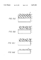
- FIG. 1(a-d) is a sectional diagram of the semiconductor chip for explaining a first embodiment of the invention
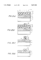
- FIG. 2(a-d) is a sectional diagram of the semiconductor chip for explaining a second embodiment of the invention.
- FIG. 3(a-d) is a sectional diagram of the semiconductor chip for explaining a third embodiment of the invention.
- FIG. 4 is a diagram showing the infrared absorption spectra of silicon dioxide films used in the prior art and in this invention.
- a silicon dioxide film 2 with thickness of about 0.8 ⁇ m is formed as a film to be etched by a chemical vapor deposition (CVD) method on a semiconductor substrate 1 consisting of silicon or the like.
- CVD chemical vapor deposition
- the substrate is heated in an N 2 gas atmosphere at 150° C. for 30 minutes to form a lower resist film 3 with thickness of about 1.5 ⁇ m.
- the surface of the lower resist film 3 is modified by exposing the substrate to the vapor of an organic silane such as hexamethyldisilazane or an organic siloxane such as hexamethyldisiloxane.
- a fluorine contained silicon dioxide film 4 with thickness of about 0.2 ⁇ m is formed on the lower resist film 3 as an intermediate film.
- an opening pattern with diameter of about 0.3 ⁇ m is formed by lithography technique.
- the upper resist film is heated in an atmosphere of N 2 gas at 130° C. for 30 minutes.
- the pattern is transferred by selective etching of the fluorine contained silicon dioxide film 4 by an RIE method using CF 4 gas or an etching method using electron cyclotron resonance (ECR) with the upper resist film as the mask.
- the lower resist film 3 is etched by an RIE method using O 2 gas carried out under a pressure of about 5 Pa, transferring the pattern and at the same time removing the upper resist layer 5.
- the silicon dioxide film 2 which is the film to be etched is selectively etched by an RIE method using CF 4 gas to transfer the pattern and to remove simultaneously the fluorine contained silicon dioxide film 4.
- a silicon dioxide film 2 having a fine opening 6 is obtained by removing the lower resist film 3 by ashing it in an O 2 plasma.
- a fluorine contained silicon dioxide film 4 as an intermediate film at room temperature with absolutely no delamination and yet with nonuniformity of less than 2% of the film thickness.
- the fluorine contained silicon dioxide film 4 will not generate shrink or cracks by heat treatment, the diameter of the opening 6 formed in the silicon dioxide film 2 had a satisfactory result of about 0.32 ⁇ m.
- a silicon dioxide film 2 with thickness of about 0.8 ⁇ m is formed on the substrate 1 by a CVD method.
- a lower wiring 10 with thickness of about 0.7 ⁇ m consisting of Al--Si--Cu, an interlayer insulating film 7 consisting of SiO 2 formed by a CVD method, and an upper wiring film 11 with thickness of about 0.7 ⁇ m consisting of Al--Si--Cu are formed sequentially.
- a step height of about 0.7 ⁇ m is generated in the upper wiring film.
- a solution having silanol Si(OH) 4 as the principal ingredient is coated on a lower resist film 3A by spin coating method and the substrate is heated for about one minute over a hot plate kept at 100° C., and the substrate is exposed at room temperature toga vapor 9 having triethoxyfluorosilane FSi(OC 2 H 5 ) 3 as the principal ingredient for 10 minutes.
- a fluorine contained SOG film 8 with thickness of about 0.2 ⁇ m containing small amount of residual moisture component (OH group, Si--OH bonding) is formed.
- an upper resist film 5A is formed by patterning using lithography technique.
- the pattern is transferred by selectively etching the fluorine contained SOG film 8 by an RIE method using CF 4 gas.
- the upper wiring film 11 is etched by an RIE method using chlorine-based gas such as CCl 4 to form an upper wiring 11A.
- the lower resist film 3A is removed by ashing it in an O 2 plasma, completing a two-level wiring as shown in FIG. 2(d).
- the second embodiment it is possible to form a high quality SOG film 8 containing fluorine at a temperature below 150° C., so the shrinkage and the strength can be improved similar to the case of the fluorine contained silicon dioxide film in the first embodiment.
- the upper wiring 11A formed by the above-mentioned process is hardly affected by the step height (about 0.7 ⁇ m) generated by the lower wiring film or the like, and the dimensional error against the design dimension of 0.6 ⁇ m was an extremely satisfactory value of ⁇ 0.05 ⁇ m in contrast to the conventional value of ⁇ 0.1 ⁇ m.
- an upper wiring with wiring spacing 0.4 ⁇ m and wiring width 0.6 ⁇ m was formed, there occurred absolutely no failure such as disconnection or short-circuiting.
- silicon dioxide film 2 with thickness of about 0.8 ⁇ m is formed by a CVD method on a semiconductor substrate 1.
- about 0.2 ⁇ m-thick titanium-containing tungsten (Ti--W) film 12 and about 0.1 ⁇ m-thick gold (Au) film 13 are formed sequentially both by sputtering.
- a photoresist film is coated, and about 1.5 ⁇ m-thick lower resist film 3B is formed by heating in an N 2 atmosphere at 130° C. for 60 minutes. In this case it is preferable that the heating temperature does not exceed 150° C. since the adhesive strength between the lower resist film 3B and the Au film 13 deteriorates and delamination takes place if the temperature is higher than 150° C.
- an about 0.2 ⁇ m-thick fluorine contained silicon dioxide film 4A is formed by a CVD method using triethoxyfluorosilane and pure water as the gas sources, under the conditions of substrate temperature 25° C. and pressure about 5 Pa.
- an upper resist film 5B is formed by patterning that employs the lithography technique.
- the fluorine contained silicon dioxide film 4A is selectively etched by an RIE method using CF 4 gas, and the pattern is transferred.
- the lower resist film 3B is etched by an RIE method that uses O 2 gas under the pressure of about 5 Pa, to transfer the pattern and form a trench 14, and to remove the upper resist film 5B at the same time.
- an about 1 ⁇ m-thick Au plated film 15 is formed in the trench 14 by electroplating method which uses the Ti--W film 12 and the Au film 13 as the electrode.
- the lower resist film 3B is removed by ashing it in an O 2 plasma.
- the Au film 13 is removed by an ion milling method except for the part that becomes the wiring.
- the Ti--W film 12 except for the part that becomes the wiring by an RIE method using a fluorine-based gas, forming an Au wiring 20 as shown in FIG. 3(d).
- the fluorine contained silicon dioxide film 4A can be formed by a low temperature CVD method according to the third embodiment, it is possible to form the lower resist film 3B at a temperature below 150° C. Accordingly, when an Au wiring of width 0.7 ⁇ m was formed, there occurred absolutely no failure such as disconnection or short-circuiting because the delamination of the Au film 13 from the lower resist film 3B can be eliminated.
- a photoresist film is used as the organic film on the film to be etched.
- a polyimide resin film instead of it a polystyrene resin film, or a film of electroconductive polymer such as polyacetylene or polypyrrole can also be used.
- the film to be etched can be an insulating film such as a silicon dioxide film, a silicon nitride film, a tantalum oxide film, or the like that is used in the manufacturing process of semiconductor devices, or can be an electroconductive film such as a polysilicon film, an Al film, a TiN film, or the like.
- silanol was used in the formation of the SOG film, but it may be replaced by a compound with structural formula Si(OR) 4 (R is an alkyl group) such as tetramethoxydisilane, or a compound with structural formula R n Si(OR) 4-n (R is an alkyl group and n is an integer from 1 to 3) such as monomethyltriethoxysilane.
Abstract
Description
Claims (11)
Applications Claiming Priority (2)
| Application Number | Priority Date | Filing Date | Title |
|---|---|---|---|
| JP4-046506 | 1992-03-04 | ||
| JP4650692 | 1992-03-04 |
Publications (1)
| Publication Number | Publication Date |
|---|---|
| US5407529A true US5407529A (en) | 1995-04-18 |
Family
ID=12749138
Family Applications (1)
| Application Number | Title | Priority Date | Filing Date |
|---|---|---|---|
| US08/027,728 Expired - Fee Related US5407529A (en) | 1992-03-04 | 1993-03-04 | Method for manufacturing semiconductor device |
Country Status (1)
| Country | Link |
|---|---|
| US (1) | US5407529A (en) |
Cited By (19)
| Publication number | Priority date | Publication date | Assignee | Title |
|---|---|---|---|---|
| US5661334A (en) * | 1996-01-16 | 1997-08-26 | Micron Technology, Inc. | Inter-metal dielectric structure which combines fluorine-doped glass and barrier layers |
| US5763010A (en) * | 1996-05-08 | 1998-06-09 | Applied Materials, Inc. | Thermal post-deposition treatment of halogen-doped films to improve film stability and reduce halogen migration to interconnect layers |
| US5767582A (en) * | 1995-06-02 | 1998-06-16 | Advanced Micro Devices, Inc. | Surface conditioning insulating layer for fine line conductive pattern |
| US5807785A (en) * | 1996-08-02 | 1998-09-15 | Applied Materials, Inc. | Low dielectric constant silicon dioxide sandwich layer |
| US5872065A (en) * | 1997-04-02 | 1999-02-16 | Applied Materials Inc. | Method for depositing low K SI-O-F films using SIF4 /oxygen chemistry |
| US5950106A (en) * | 1996-05-14 | 1999-09-07 | Advanced Micro Devices, Inc. | Method of patterning a metal substrate using spin-on glass as a hard mask |
| US5962346A (en) * | 1997-12-29 | 1999-10-05 | Taiwan Semiconductor Manufacturing Company, Ltd. | Fluorine-doped silicate glass hard mask to improve metal line etching profile |
| US6103601A (en) * | 1995-10-26 | 2000-08-15 | Applied Materials, Inc. | Method and apparatus for improving film stability of halogen-doped silicon oxide films |
| US6136680A (en) * | 2000-01-21 | 2000-10-24 | Taiwan Semiconductor Manufacturing Company | Methods to improve copper-fluorinated silica glass interconnects |
| US6174754B1 (en) | 2000-03-17 | 2001-01-16 | Taiwan Semiconductor Manufacturing Company | Methods for formation of silicon-on-insulator (SOI) and source/drain-on-insulator(SDOI) transistors |
| US6214659B1 (en) * | 1998-09-22 | 2001-04-10 | United Microelectronics Corp. | Method to crown capacitor for high density DRAM |
| US6331480B1 (en) * | 1999-02-18 | 2001-12-18 | Taiwan Semiconductor Manufacturing Company | Method to improve adhesion between an overlying oxide hard mask and an underlying low dielectric constant material |
| US6358838B2 (en) * | 2000-01-18 | 2002-03-19 | Hitachi, Ltd. | Semiconductor device and process for producing the same |
| US6410453B1 (en) * | 1999-09-02 | 2002-06-25 | Micron Technology, Inc. | Method of processing a substrate |
| US6413358B2 (en) | 1993-04-16 | 2002-07-02 | Micron Technology, Inc. | Method and apparatus for improving etch uniformity in remote source plasma reactors with powered wafer chucks |
| US6451686B1 (en) | 1997-09-04 | 2002-09-17 | Applied Materials, Inc. | Control of semiconductor device isolation properties through incorporation of fluorine in peteos films |
| US6479879B1 (en) * | 2000-11-16 | 2002-11-12 | Advanced Micro Devices, Inc. | Low defect organic BARC coating in a semiconductor structure |
| US6591634B1 (en) * | 1994-02-25 | 2003-07-15 | Toshinori Morizane | Method for production of metal oxide glass film at a low temperature |
| US20180034007A1 (en) * | 2015-08-03 | 2018-02-01 | Boe Technology Group Co., Ltd. | Electrode Structure and Organic Light Emitting Unit and Manufacturing Method Thereof |
Citations (1)
| Publication number | Priority date | Publication date | Assignee | Title |
|---|---|---|---|---|
| JPS6425543A (en) * | 1987-07-22 | 1989-01-27 | Hitachi Ltd | Manufacture of film including silicon oxide |
-
1993
- 1993-03-04 US US08/027,728 patent/US5407529A/en not_active Expired - Fee Related
Patent Citations (1)
| Publication number | Priority date | Publication date | Assignee | Title |
|---|---|---|---|---|
| JPS6425543A (en) * | 1987-07-22 | 1989-01-27 | Hitachi Ltd | Manufacture of film including silicon oxide |
Cited By (24)
| Publication number | Priority date | Publication date | Assignee | Title |
|---|---|---|---|---|
| US6500300B2 (en) | 1993-04-16 | 2002-12-31 | Micron Technology, Inc. | Plasma reactor |
| US20050173376A1 (en) * | 1993-04-16 | 2005-08-11 | Donohoe Kevin G. | Method for etching a wafer in a plasma etch reactor |
| US6946053B2 (en) | 1993-04-16 | 2005-09-20 | Micron Technology, Inc. | Plasma reactor |
| US6413358B2 (en) | 1993-04-16 | 2002-07-02 | Micron Technology, Inc. | Method and apparatus for improving etch uniformity in remote source plasma reactors with powered wafer chucks |
| US6591634B1 (en) * | 1994-02-25 | 2003-07-15 | Toshinori Morizane | Method for production of metal oxide glass film at a low temperature |
| US5767582A (en) * | 1995-06-02 | 1998-06-16 | Advanced Micro Devices, Inc. | Surface conditioning insulating layer for fine line conductive pattern |
| US6103601A (en) * | 1995-10-26 | 2000-08-15 | Applied Materials, Inc. | Method and apparatus for improving film stability of halogen-doped silicon oxide films |
| US5661334A (en) * | 1996-01-16 | 1997-08-26 | Micron Technology, Inc. | Inter-metal dielectric structure which combines fluorine-doped glass and barrier layers |
| US6079354A (en) * | 1996-05-08 | 2000-06-27 | Applied Materials, Inc. | Thermal post-deposition treatment of halogen-doped films to improve film stability and reduce halogen migration to interconnect layers |
| US5763010A (en) * | 1996-05-08 | 1998-06-09 | Applied Materials, Inc. | Thermal post-deposition treatment of halogen-doped films to improve film stability and reduce halogen migration to interconnect layers |
| US5950106A (en) * | 1996-05-14 | 1999-09-07 | Advanced Micro Devices, Inc. | Method of patterning a metal substrate using spin-on glass as a hard mask |
| US5807785A (en) * | 1996-08-02 | 1998-09-15 | Applied Materials, Inc. | Low dielectric constant silicon dioxide sandwich layer |
| US5872065A (en) * | 1997-04-02 | 1999-02-16 | Applied Materials Inc. | Method for depositing low K SI-O-F films using SIF4 /oxygen chemistry |
| US6451686B1 (en) | 1997-09-04 | 2002-09-17 | Applied Materials, Inc. | Control of semiconductor device isolation properties through incorporation of fluorine in peteos films |
| US5962346A (en) * | 1997-12-29 | 1999-10-05 | Taiwan Semiconductor Manufacturing Company, Ltd. | Fluorine-doped silicate glass hard mask to improve metal line etching profile |
| US6214659B1 (en) * | 1998-09-22 | 2001-04-10 | United Microelectronics Corp. | Method to crown capacitor for high density DRAM |
| US6331480B1 (en) * | 1999-02-18 | 2001-12-18 | Taiwan Semiconductor Manufacturing Company | Method to improve adhesion between an overlying oxide hard mask and an underlying low dielectric constant material |
| US6410453B1 (en) * | 1999-09-02 | 2002-06-25 | Micron Technology, Inc. | Method of processing a substrate |
| US6358838B2 (en) * | 2000-01-18 | 2002-03-19 | Hitachi, Ltd. | Semiconductor device and process for producing the same |
| US6680541B2 (en) | 2000-01-18 | 2004-01-20 | Hitachi, Ltd. | Semiconductor device and process for producing the same |
| US6136680A (en) * | 2000-01-21 | 2000-10-24 | Taiwan Semiconductor Manufacturing Company | Methods to improve copper-fluorinated silica glass interconnects |
| US6174754B1 (en) | 2000-03-17 | 2001-01-16 | Taiwan Semiconductor Manufacturing Company | Methods for formation of silicon-on-insulator (SOI) and source/drain-on-insulator(SDOI) transistors |
| US6479879B1 (en) * | 2000-11-16 | 2002-11-12 | Advanced Micro Devices, Inc. | Low defect organic BARC coating in a semiconductor structure |
| US20180034007A1 (en) * | 2015-08-03 | 2018-02-01 | Boe Technology Group Co., Ltd. | Electrode Structure and Organic Light Emitting Unit and Manufacturing Method Thereof |
Similar Documents
| Publication | Publication Date | Title |
|---|---|---|
| US5407529A (en) | Method for manufacturing semiconductor device | |
| KR100295043B1 (en) | Method for forming a metal film of a semiconductor device using an insulating film having a low dielectric constant as an interdielectric layer | |
| US4692205A (en) | Silicon-containing polyimides as oxygen etch stop and dual dielectric coatings | |
| EP0046525B1 (en) | Planar multi-level metal-insulator structure comprising a substrate, a conductive interconnection pattern and a superposed conductive structure and a method to form such a structure | |
| US6420261B2 (en) | Semiconductor device manufacturing method | |
| US7256136B2 (en) | Self-patterning of photo-active dielectric materials for interconnect isolation | |
| KR100358545B1 (en) | Semiconductor device and process for producing the same | |
| JP3226021B2 (en) | Method for manufacturing semiconductor device | |
| GB2319891A (en) | Low dielectric constant interlayer insulators | |
| JP3193335B2 (en) | Method for manufacturing semiconductor device | |
| US5306947A (en) | Semiconductor device and manufacturing method thereof | |
| US4447824A (en) | Planar multi-level metal process with built-in etch stop | |
| JPH06208993A (en) | Manufacture of semiconductor device | |
| US5393709A (en) | Method of making stress released VLSI structure by the formation of porous intermetal layer | |
| JPS60142545A (en) | Multilayer composite structure | |
| JPH10163198A (en) | Semiconductor device and its manufacture | |
| JPH0653134A (en) | Manufacture of semiconductor device | |
| JPS58140139A (en) | Semiconductor device and manufacture thereof | |
| JP2873759B2 (en) | Pretreatment method for wet etching of semiconductor device | |
| JP2757618B2 (en) | Method for manufacturing semiconductor device | |
| JPS6011458B2 (en) | Manufacturing method of semiconductor device | |
| JPS61154148A (en) | Manufacture of semiconductor device | |
| KR920000831B1 (en) | Metalized multi-layer of semiconductor elements | |
| JPH0684901A (en) | Method of manufacturing semiconductor device | |
| JP2000349151A (en) | Semiconductor device and method of manufacturing it |
Legal Events
| Date | Code | Title | Description |
|---|---|---|---|
| AS | Assignment |
Owner name: NEC CORPORATION, JAPAN Free format text: ASSIGNMENT OF ASSIGNORS INTEREST.;ASSIGNOR:HOMMA, TETSUYA;REEL/FRAME:006474/0541 Effective date: 19930302 |
|
| FEPP | Fee payment procedure |
Free format text: PAYOR NUMBER ASSIGNED (ORIGINAL EVENT CODE: ASPN); ENTITY STATUS OF PATENT OWNER: LARGE ENTITY |
|
| FPAY | Fee payment |
Year of fee payment: 4 |
|
| FPAY | Fee payment |
Year of fee payment: 8 |
|
| AS | Assignment |
Owner name: NEC ELECTRONICS CORPORATION, JAPAN Free format text: ASSIGNMENT OF ASSIGNORS INTEREST;ASSIGNOR:NEC CORPORATION;REEL/FRAME:013758/0440 Effective date: 20021101 |
|
| REMI | Maintenance fee reminder mailed | ||
| LAPS | Lapse for failure to pay maintenance fees | ||
| STCH | Information on status: patent discontinuation |
Free format text: PATENT EXPIRED DUE TO NONPAYMENT OF MAINTENANCE FEES UNDER 37 CFR 1.362 |
|
| FP | Lapsed due to failure to pay maintenance fee |
Effective date: 20070418 |