US5413679A - Method of producing a silicon membrane using a silicon alloy etch stop layer - Google Patents
Method of producing a silicon membrane using a silicon alloy etch stop layer Download PDFInfo
- Publication number
- US5413679A US5413679A US08/083,952 US8395293A US5413679A US 5413679 A US5413679 A US 5413679A US 8395293 A US8395293 A US 8395293A US 5413679 A US5413679 A US 5413679A
- Authority
- US
- United States
- Prior art keywords
- silicon
- silicon substrate
- etch stop
- membrane
- stop layer
- Prior art date
- Legal status (The legal status is an assumption and is not a legal conclusion. Google has not performed a legal analysis and makes no representation as to the accuracy of the status listed.)
- Expired - Fee Related
Links
Images


Classifications
-
- G—PHYSICS
- G01—MEASURING; TESTING
- G01L—MEASURING FORCE, STRESS, TORQUE, WORK, MECHANICAL POWER, MECHANICAL EFFICIENCY, OR FLUID PRESSURE
- G01L9/00—Measuring steady of quasi-steady pressure of fluid or fluent solid material by electric or magnetic pressure-sensitive elements; Transmitting or indicating the displacement of mechanical pressure-sensitive elements, used to measure the steady or quasi-steady pressure of a fluid or fluent solid material, by electric or magnetic means
- G01L9/0041—Transmitting or indicating the displacement of flexible diaphragms
- G01L9/0042—Constructional details associated with semiconductive diaphragm sensors, e.g. etching, or constructional details of non-semiconductive diaphragms
-
- Y—GENERAL TAGGING OF NEW TECHNOLOGICAL DEVELOPMENTS; GENERAL TAGGING OF CROSS-SECTIONAL TECHNOLOGIES SPANNING OVER SEVERAL SECTIONS OF THE IPC; TECHNICAL SUBJECTS COVERED BY FORMER USPC CROSS-REFERENCE ART COLLECTIONS [XRACs] AND DIGESTS
- Y10—TECHNICAL SUBJECTS COVERED BY FORMER USPC
- Y10S—TECHNICAL SUBJECTS COVERED BY FORMER USPC CROSS-REFERENCE ART COLLECTIONS [XRACs] AND DIGESTS
- Y10S438/00—Semiconductor device manufacturing: process
- Y10S438/97—Specified etch stop material
-
- Y—GENERAL TAGGING OF NEW TECHNOLOGICAL DEVELOPMENTS; GENERAL TAGGING OF CROSS-SECTIONAL TECHNOLOGIES SPANNING OVER SEVERAL SECTIONS OF THE IPC; TECHNICAL SUBJECTS COVERED BY FORMER USPC CROSS-REFERENCE ART COLLECTIONS [XRACs] AND DIGESTS
- Y10—TECHNICAL SUBJECTS COVERED BY FORMER USPC
- Y10S—TECHNICAL SUBJECTS COVERED BY FORMER USPC CROSS-REFERENCE ART COLLECTIONS [XRACs] AND DIGESTS
- Y10S438/00—Semiconductor device manufacturing: process
- Y10S438/977—Thinning or removal of substrate
Landscapes
- Chemical & Material Sciences (AREA)
- Analytical Chemistry (AREA)
- Physics & Mathematics (AREA)
- General Physics & Mathematics (AREA)
- Weting (AREA)
Abstract
A method of producing a silicon membrane has a step of forming an etch stop layer on an upper surface of a silicon substrate having lower and upper opposing surfaces, the etch stop layer comprising an alloy of silicon and at least one other Group IV element. The method of producing a silicon membrane has another step of forming a cap layer on the etch stop layer, the cap layer having lower and upper opposing surfaces with the lower surface contacting the etch stop layer. The method of producing a silicon membrane has a further step of removing a portion of the silicon substrate at a time when the upper surface of the cap layer is exposed, the portion of the silicon substrate being removed extending from the upper surface of the silicon substrate to the lower surface of the silicon substrate to thereby define an exposed portion of the etch stop layer. The exposed portion of the etch stop layer may be removed. Also, the formed membrane can be further processed to define undoped device structures isolated by thin silicon legs. According to another embodiment, a cap layer is never formed and the etch stop layer itself functions as the membrane.
Description
1. Field of the Invention
The present invention relates to a method of forming membranes in general, and, more specifically, to a method of forming silicon membranes in which a silicon device is to be formed.
2. Description of the Related Art
In the past, thin silicon membranes suspended by a substrate, such as a silicon substrate, have been used in several fields. These fields include x-ray lithography in which a thin suspended silicon membrane, which is transparent to X rays, is coated with a metal such as gold. The coated membrane is then used as a mask for X rays.
Thin silicon membranes have also been used for specialty electronic devices such as air bridges in fast transistors. Another example of such specialty electronic devices is a balometer, which detects single photons to measure heat, for example an x-ray balometer.
Among the prior methods of forming silicon membranes is a method in which a silicon boron layer is formed on a silicon substrate. A silicon cap layer is then formed on the silicon boron layer. A portion of the silicon substrate is then removed by etching, with the silicon boron layer serving as an etch stop. Finally, the silicon boron layer may or may not be removed to form a silicon membrane.
There are several problems associated with using silicon boron as the etch stop layer in forming silicon membranes. For example, it is sometimes necessary that the silicon membrane be as free as possible from impurities. In fact, intrinsic silicon is often desired. However, boron, because it is a fast diffuser in silicon, easily diffuses into the silicon membrane 7 leaving a residual impurity after the silicon boron layer is removed.
A further problem is encountered when the silicon membrane is used to form certain specialty electronic devices requiring intrinsic silicon of high carrier mobility. Since boron is a p-type dopant in silicon, the residual boron doped tail must be removed in a further processing step.
Still further, if the silicon membrane is crystalline and a high level of boron impurities is present, the crystal lattice is subjected to stresses that may cause the formation of dislocations in the material. Furthermore, for the silicon boron layer to function as an effective etch stop, the silicon must be doped with boron to at least 1×10²⁰ atoms/cm3, with a resulting boron concentration of at least 0.2%. With this high concentration of boron, the likelihood of boron diffusing into the silicon membrane is high.
U.S. Pat. No. 5,013,681, which has the same Assignee as, and a common inventor with, the present invention, proposes using a silicon germanium etch stop layer in the formation of silicon on insulator substrates. However, such a silicon germanium etch stop layer has never been proposed in the processing field which concerns, for example, x-ray lithography, or in the specialty electronics field of balometers and the like.
Accordingly, it is an object of the present invention to provide a method of forming a silicon membrane which is free from impurities.
It is a further object of the present invention to provide a method of forming a silicon membrane which is undoped and does not cause phonon scattering when used to form devices such as balometers.
It is a still further object of the invention to provide a method of forming a silicon membrane which is not subjected to internal stresses to the degree as are those of the prior art.
According to the present invention, a silicon germanium layer (or alloy layer of silicon and at least one other group IV element) is used as the etch stop layer in forming a silicon membrane. Alternatively, the silicon germanium layer itself may be used as the membrane. The germanium atom is larger than the silicon atom, and germanium is therefore not as free to diffuse into the silicon cap layer.
Germanium impurities in the silicon lattice put the adjacent silicon atoms in compression because the germanium atom is larger than the silicon atom. However, because the silicon germanium etch stop layer results in fewer impurities in the silicon membrane, the silicon membrane is not subjected to internal stresses to the same degree as a prior art membrane.
The accompanying drawings illustrate several aspects of the present invention, and together with the detailed description, serve to explain the principles of the present invention. Throughout the drawings, like numerals depict like elements. In the drawings:
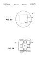
FIG. 1A is a cross-sectional view of an etch stop layer deposited on a silicon substrate according to a first embodiment of the present invention;
FIG. 1B is a cross-sectional view of the structure of FIG. 1A after a mask has been deposited on a lower surface of the silicon substrate according to the first embodiment of the present invention;
FIG. 1C is a bottom plan view showing the structure of FIG. 1B after a portion of the lower surface of the silicon substrate has been exposed through the mask according to the first embodiment of the present invention;
FIG. 1D is a cross-sectional view of the structure of FIG. 1C after a portion of the silicon substrate has been removed according to the first embodiment of the present invention;
FIG. 2A is a cross-sectional view of an etch stop layer deposited on a silicon substrate according to a second embodiment of the present invention;
FIG. 2B is a cross-sectional view of the structure of FIG. 2A after a cap layer has been formed on the etch stop layer according to the second embodiment of the present invention;
FIG. 2C is a cross-sectional view showing the structure of FIG. 2B after a mask has been deposited on the upper surface of the cap layer according to the second embodiment of the present invention;
FIG. 2D is a cross-sectional view of the structure of FIG. 2C after a mask has been deposited on a lower surface of the silicon substrate according to the second embodiment of the present invention;
FIG. 2E is a bottom plan view showing the structure of FIG. 2D after a portion of the lower surface of the silicon substrate has been exposed through the mask according to the second embodiment of the present invention;
FIG. 2F is a cross-sectional view of the structure of FIG. 2E according to the second embodiment of the present invention;
FIG. 2G is a cross-sectional view of the structure of FIG. 2F after an exposed portion of the etch stop layer has been removed according to the second embodiment of the present invention;
FIG. 2H is a cross-sectional view of the structure of FIG. 2G after the mask has been removed from the upper surface of the cap layer according to the second embodiment of the present invention;
FIG. 3A is a top plan view of the structure of FIG. 2H showing the upper surface of the cap layer according to a modification of the second embodiment of the present invention; and
FIG. 3B is a view of the silicon device area and the peripheral area after a portion of the peripheral area has been removed according to the modification of the second embodiment of the present invention.
According to a first embodiment of the present invention, an etch stop layer 3 itself is used as the thin supported membrane. As shown in FIG. 1A, the etch stop layer 3 is first formed on an upper surface of a silicon substrate 1. This is done by chemically cleaning the silicon substrate (wafer) 1 using a standard cleaning procedure. The cleaned substrate 1 is then loaded into a conventional system capable of growing epitaxial silicon or germanium. Both molecular beam epitaxy (MBE) and chemical vapor deposition (CVD) are currently viable means of epitaxial growth. Following a brief degassing and loading of the substrate 1 into the growth chamber, the silicon oxide present is conventionally removed in situ, typically by heating to 700°-1100° C. When MBE is used as the growth means, the temperature is preferably 750°-950° C., and most preferably, 800°-900° C. Oxide removal is also possible by heating in a silicon flux (for MBE processes), by bombardment by noble gas ions (for MBE processes), or by heating in H2 flux (for CVD processes ) .
If desired, a silicon buffer may then be conventionally grown on the silicon substrate 1. This step is not shown in the figures. The silicon buffer layer helps to obtain a smooth silicon surface with no pitting or holes. This buffer layer may be grown, for example, at approximately 650° C., with a thickness of 100 Å to 1.0 μm thick.
The etch stop layer 3 is now grown on the buffer layer, if present, or on the silicon substrate 1. The etch stop layer 3 can be grown by conventional techniques, such as molecular beam epitaxy or chemical vapor deposition. These growth techniques are well developed and generate a sharp silicon/alloy interface. The etch stop layer 3 may be Si1-x GeX alloy, where x is typically about 0.1 to about 0.5. More preferably, x is about 0.20 to about 0.4, and most preferably, the etch stop layer 3 is a Si0.7 Ge0.3 alloy, and is grown at about 400° to about 900° C.
Although the etch stop layer 3 is described above as being a silicon germanium alloy, etch stop layer 3 can be an alloy of silicon and any other Group IV element (carbon, germanium, tin, or lead). The etch stop layer 3 has lower (3a) and upper (3b) opposing surfaces with the lower surface 3a contacting the silicon substrate 1.
Following the step of forming an etch stop layer 3 on the silicon substrate 1, a portion of the silicon substrate 1 is removed. This can be done by several different conventional methods. As shown in FIG. 1B, it can be accomplished by depositing a mask layer 7 on the lower surface of the silicon substrate 1 with a conventional technique. The mask may be silicon oxide, silicon nitride, or a metal, for example. The mask may be defined by depositing a photoresist thereon. Any one of a variety of commonly available photoresists can be used, including a 1400-26 Shipley™ brand photoresist. Then, the photoresist 7 is exposed and developed by conventional techniques to define an exposed portion of the mask 7. The mask is defined through the photoresist using a buffered oxide etch, for example. Portion 8 of the lower surface of the silicon substrate 1 is exposed through the mask layer 7. Mechanical polishing can be used to remove the majority of the silicon. Alternatively, chemical techniques may be used initially. For example, hydrofluoric-nitric-acetic (HNA) solution, or KOH, as a possible first etch, may be introduced onto the exposed portion of the lower surface of the silicon substrate 1. The use of HNA is discussed in Muraoka et al. in a chapter entitled "Controlled Preferential Etching Technology" appearing in the book Silicon Semiconductor 1973, incorporated herein by reference in its entirety for all purposes. When the chemical technique is used, the first etch removes the majority of the silicon substrate, leaving approximately 1-2 μm of silicon below the etch stop layer 3. After the initial chemical or mechanical technique, the silicon substrate 1 is cleaned and placed into a selective etch bath. The remaining silicon substrate 1 to be removed is stripped away by a selective etchant (second etch) composed of, for example, 100 g KOH, 4 g K2 Cr2 O7 and 100 ml. propanol in 400 ml. of water at 25° C. in a temperature controlled rotary etch system. This second etch is described in P. Narozny et al, "Si/SiGe Heterojunction Bipolar Transistor with Graded Gap SiGe Base Made by Molecular Beam Epitaxy" IEEE Journal, August 1988, pages 562-565, which is hereby incorporated by reference in its entirety for all purposes. The resulting structure is shown in FIG. 1D. Because the object of the method is to form a suspended membrane, the silicon substrate 1 is removed at a time when the upper surface of the etch stop layer 3 is exposed.
According to a second embodiment of the present invention, a cap layer 5 is formed on the etch stop layer 3 by a method which will be described later. The method of the second embodiment is illustrated in FIGS. 2A through 2F, in which the like numerals depict like elements. Therefore, a description of the like elements is omitted, where appropriate.
According to the method of the second embodiment, the etch stop layer 3 is first formed on the upper surface of the silicon substrate 1, as shown in FIG. 2A. The etch stop layer 3 is formed using the same techniques as were used in the first embodiment.
Then, as shown in FIG. 2B, a cap layer 5 is formed on the etch stop layer 3, preferably epitaxially. The cap layer 5 is typically grown on the etch stop layer 3 at about 400° to about 1100° C. (e.g., typically about 500° to about 800° C. for MBE processes). The thickness of the cap layer 5 is 50 to 1000 nm, and more preferably 100 to 500 nm. The cap layer 5 has lower and upper opposing surfaces with the lower surface contacting the etch stop layer 3. The cap layer 5 is preferably a silicon cap layer 5.
It may be desirable to protect the upper surface of the cap layer 5 from damage possibly incurred in a later silicon substrate 1 removal step and subsequent steps. This can be done by a variety of conventional techniques including depositing a conventional mask layer 11 on the upper surface of the cap layer 5, as shown in FIG. 2C.
Next, a portion of the silicon substrate 1 is removed in the same manner as described above in the first embodiment of the present invention and as shown in FIGS. 2D and 2E. As can be seen in FIG. 2F, removal of the portion of the silicon substrate 1 defines an exposed portion of the etch stop layer 3.
If the mask 11 is not used, the portion of the silicon substrate 1 is removed at a time when the upper surface of the cap layer 5 is exposed. However, if the mask 11 is used, then the cap layer 5 is covered when the portion of the silicon substrate 1 is removed. In this case, an upper surface of the mask 11 is exposed when the portion of the silicon substrate 1 is removed (in the same manner as described for the first embodiment).
The exposed portion of the etch stop layer 3 can then be conventionally removed with the resulting structure shown in FIG. 2G. To remove the etch stop layer 3 a solution of nitric acid, hydrofluoric acid and water can be used, as described in Krist et al. , "Selective Removal of a Si0.7 Ge0.3 Layer From Si(100)", App. , Phys. Lett., 58(17), 29 Apr. 1991 incorporated by reference herein in its entirety for all purposes. The etch stop layer 3 can also be left intact and not removed.
Finally, the mask 11, if used, would be removed by conventional techniques. The resulting structure is shown in FIG. 2H.
A modification of the second embodiment of the present invention is directed to forming specialty electronic devices on the cap layer 5. FIG. 3A is a top plan view of the structure of FIG. 2H and shows the cap layer 5. The area within the dotted line is a membrane suspended by the silicon substrate 1. The silicon substrate 1 has been removed from under the area shown by the dotted line. Reference numeral 13 represents a silicon device area and a peripheral area of the cap layer 5. A fast transistor or a balometer can be formed on the silicon device area. Reference numeral 15 represents a remainder area of the silicon cap layer 5. That is, reference numeral 15 is all portions of the suspended membrane, the area within the dotted line, except the silicon device area and the peripheral area.
As can be seen from FIG. 3B, the silicon device area 17 is surrounded by the peripheral area 19. FIG. 3B is an enlarged view of the silicon device area and the peripheral area 19 of the silicon cap layer 5 of FIG. 3A after a portion of the peripheral area 19 has been removed. According to this modification of the second embodiment, a portion of the peripheral area 19 is removed by the same techniques in which the silicon substrate 1 was removed. That is, a mask of silicon oxide, silicon nitride or a metal, for example, is deposited and defined using conventional lithographic techniques, for example, a buffered oxide etch. Then, using a photoresist and conventional lithographic techniques the mask is defined. Then, the cap layer 5 is etched, as described above. The portion of the peripheral area 19 removed defines at least one connecting leg 21 of any shape and length which connects the silicon device area 17 to the remainder portion 15 (see FIG. 3A).
The device area is particularly appropriate for forming a balometer thereon. The device area provides low thermal mass and low thermal conductivity between the balometer and the supporting structure as well as electrical and mechanical isolation. These properties are ideal for balometers.
Numerous modifications and variations of the present invention are possible in light of the above teachings. It is therefore to be understood that within the scope of the appended claims, the invention may be practiced otherwise than as specifically described herein.
Claims (20)
1. A method of producing a membrane, comprising the steps of:
(a) forming an etch stop layer on an upper surface of a silicon substrate having upper and lower surfaces, the etch stop layer comprising an alloy of silicon and at least one other Group IV element, the etch stop layer having lower and upper surfaces with the lower surface contacting the silicon substrate; and
(b) removing a portion of the silicon substrate with the upper surface of the etch stop layer exposed, the portion of the silicon substrate being removed extending from the upper surface of the silicon substrate to the lower surface of the silicon substrate.
2. The method of forming a membrane as recited in claim 1, wherein the etch stop layer comprises a silicon germanium alloy.
3. The method of producing a membrane as claimed in claim 1, wherein step (b) includes the substep of mechanically grinding or polishing the silicon substrate to remove all but 1-3 μm of the removed portion of the silicon substrate.
4. The method of producing a membrane as claimed in claim 1, wherein step (b) includes the sub-steps of:
depositing a mask layer on the lower surface of the silicon substrate;
removing a portion of the mask layer to define an exposed portion of the lower surface of the silicon substrate; and
etching the exposed portion of the lower surface of the silicon substrate.
5. A method of producing a membrane, comprising the steps of:
(a) forming an etch stop layer on an upper surface of a silicon substrate having lower and upper surfaces, the etch stop layer comprising an alloy of silicon and at least one other Group IV element;
(b) forming a cap layer on the etch stop layer, the cap layer having lower and upper surfaces, the lower surface contacting the etch stop layer; and
(c) removing a portion of the silicon substrate with the upper surface of the cap layer exposed, the portion of the silicon substrate being removed extending from the upper surface of the silicon substrate to the lower surface of the silicon substrate and defining an exposed portion of the etch stop layer.
6. The method of forming a membrane as recited in claim 5, wherein the etch stop layer comprises a silicon germanium alloy.
7. The method of producing a membrane as claimed in claim 5, further comprising the step of removing the exposed portion of the etch stop layer.
8. The method of producing a membrane as claimed in claim 5, wherein the cap layer is a silicon cap layer.
9. The method of producing a membrane as claimed in claim 5, wherein the cap layer is an epitaxial silicon cap layer.
10. The method of producing a membrane as claimed in claim 9, wherein the silicon cap layer has a thickness approximately of 10-500 nm.
11. The method of producing a membrane as claimed in claim 5, where in step (b) includes the substep of mechanically grinding or polishing the silicon substrate to remove all but 1-3 μm of the removed portion of the silicon substrate.
12. The method of producing a membrane as claimed in claim 5, wherein step (b) includes the steps of:
depositing a mask layer on the lower surface of the silicon substrate;
removing a portion of the mask layer to define an exposed portion of the lower surface of the silicon substrate; and
etching the exposed portion of the lower surface of the silicon substrate.
13. The method of producing a membrane as claimed in claim 5, further comprising the step of removing a portion of the mask layer to define an exposed portion of the lower surface of the silicon substrate.
14. A method of producing a membrane, comprising the steps of:
(a) forming an etch stop layer on an upper surface of a silicon substrate having upper and lower surfaces, the etch stop layer comprising an alloy of silicon and germanium;
(b) forming a silicon cap layer on the etch stop layer, the silicon cap layer defining a silicon device area and a peripheral area surrounding the silicon device area and having lower and upper surfaces, with the lower surface contracting the etch stop layer;
(c) depositing a mask layer on the lower surface of the silicon substrate;
(d) removing a portion of the mask layer to define an exposed portion of the lower surface of the silicon substrate;
(e) etching the silicon substrate to remove a portion of the silicon substrate extending from the exposed portion of the lower surface of the silicon substrate to the upper surface of the silicon substrate and defining an exposed portion of the etch stop layer, the portion of the silicon substrate being removed with the upper surface of the silicon cap layer exposed;
(f) removing the exposed portion of the etch stop layer; and
(g) removing a portion of the peripheral area of the silicon cap layer from the lower surface of the silicon cap layer to the upper surface thereof.
15. The method of producing a membrane as claimed in claim 14, wherein the silicon cap layer has a remainder portion surrounding the peripheral area and the peripheral area is removed to define at least one leg connecting the silicon device area to the remainder portion.
16. The method of producing a membrane as claimed in claim 14, further comprising the step of (h) forming a device on the silicon device area of the silicon cap layer.
17. The method of producing a membrane as claimed in claim 14, wherein the silicon cap layer is an epitaxial silicon cap layer.
18. The method of producing a membrane as claimed in claim 17, wherein the silicon cap layer has a thickness of approximately 10-500 microns.
19. A method of producing a membrane, comprising the steps of:
(a) forming an etch stop layer on an upper surface of a silicon substrate having lower and upper surfaces, the etch stop layer comprising an alloy of silicon and at least one other Group IV element;
(b) forming a cap layer on the etch stop layer;
(c) depositing a mask on the cap layer, the mask having lower and upper surfaces, with the lower surface contacting the cap layer; and
(d) removing a portion of the silicon substrate at a time when the upper surface of the mask is exposed, the portion of the silicon substrate being removed extending from the upper surface of the silicon substrate to the lower surface of the silicon substrate and defining an exposed portion of the etch stop layer.
20. The method of producing a membrane as claimed in claim 19, wherein the cap layer defines a silicon device area and a peripheral area surrounding the silicon device area, the method further comprising the step of (e) removing a portion of the peripheral area of the silicon cap layer from the lower surface of the silicon cap layer to the upper surface thereof.
Priority Applications (1)
| Application Number | Priority Date | Filing Date | Title |
|---|---|---|---|
| US08/083,952 US5413679A (en) | 1993-06-30 | 1993-06-30 | Method of producing a silicon membrane using a silicon alloy etch stop layer |
Applications Claiming Priority (1)
| Application Number | Priority Date | Filing Date | Title |
|---|---|---|---|
| US08/083,952 US5413679A (en) | 1993-06-30 | 1993-06-30 | Method of producing a silicon membrane using a silicon alloy etch stop layer |
Publications (1)
| Publication Number | Publication Date |
|---|---|
| US5413679A true US5413679A (en) | 1995-05-09 |
Family
ID=22181723
Family Applications (1)
| Application Number | Title | Priority Date | Filing Date |
|---|---|---|---|
| US08/083,952 Expired - Fee Related US5413679A (en) | 1993-06-30 | 1993-06-30 | Method of producing a silicon membrane using a silicon alloy etch stop layer |
Country Status (1)
| Country | Link |
|---|---|
| US (1) | US5413679A (en) |
Cited By (58)
| Publication number | Priority date | Publication date | Assignee | Title |
|---|---|---|---|---|
| WO1996015550A1 (en) * | 1994-11-10 | 1996-05-23 | Lawrence Semiconductor Research Laboratory, Inc. | Silicon-germanium-carbon compositions and processes thereof |
| US5793913A (en) * | 1996-07-10 | 1998-08-11 | Northern Telecom Limited | Method for the hybrid integration of discrete elements on a semiconductor substrate |
| US5893727A (en) * | 1993-09-28 | 1999-04-13 | Trw Inc. | Method for manufacturing a massive parallel interconnection attachment using flexible circuit |
| WO1999053539A1 (en) * | 1998-04-10 | 1999-10-21 | Massachusetts Institute Of Technology | Silicon-germanium etch stop layer system |
| US20020084000A1 (en) * | 1997-06-24 | 2002-07-04 | Eugene A. Fitzgerald | Controlling threading dislocation densities in Ge on Si using graded GeSi layers and planarization |
| US6458672B1 (en) | 1997-05-12 | 2002-10-01 | Silicon Genesis Corporation | Controlled cleavage process and resulting device using beta annealing |
| US6486041B2 (en) | 1997-05-12 | 2002-11-26 | Silicon Genesis Corporation | Method and device for controlled cleaving process |
| US6500732B1 (en) | 1999-08-10 | 2002-12-31 | Silicon Genesis Corporation | Cleaving process to fabricate multilayered substrates using low implantation doses |
| US6513564B2 (en) | 1999-08-10 | 2003-02-04 | Silicon Genesis Corporation | Nozzle for cleaving substrates |
| US20030034529A1 (en) * | 2000-12-04 | 2003-02-20 | Amberwave Systems Corporation | CMOS inverter and integrated circuits utilizing strained silicon surface channel MOSFETs |
| US6544862B1 (en) | 2000-01-14 | 2003-04-08 | Silicon Genesis Corporation | Particle distribution method and resulting structure for a layer transfer process |
| US6548382B1 (en) | 1997-07-18 | 2003-04-15 | Silicon Genesis Corporation | Gettering technique for wafers made using a controlled cleaving process |
| US20030077867A1 (en) * | 2001-03-02 | 2003-04-24 | Fitzergald Eugene A. | Relaxed silicon germanium platform for high speed CMOS electronics and high speed analog circuits |
| US6559058B1 (en) * | 2002-01-31 | 2003-05-06 | The Regents Of The University Of California | Method of fabricating three-dimensional components using endpoint detection |
| US6573126B2 (en) | 2000-08-16 | 2003-06-03 | Massachusetts Institute Of Technology | Process for producing semiconductor article using graded epitaxial growth |
| US20030102498A1 (en) * | 2001-09-24 | 2003-06-05 | Glyn Braithwaite | RF circuits including transistors having strained material layers |
| US20030113948A1 (en) * | 2000-01-20 | 2003-06-19 | Amberwave Systems Corporation | Low threading dislocation density relaxed mismatched epilayers without high temperature growth |
| US20030124815A1 (en) * | 1999-08-10 | 2003-07-03 | Silicon Genesis Corporation | Cleaving process to fabricate multilayered substrates using low implantation doses |
| US6602613B1 (en) | 2000-01-20 | 2003-08-05 | Amberwave Systems Corporation | Heterointegration of materials using deposition and bonding |
| US6649480B2 (en) | 2000-12-04 | 2003-11-18 | Amberwave Systems Corporation | Method of fabricating CMOS inverter and integrated circuits utilizing strained silicon surface channel MOSFETs |
| US20030227029A1 (en) * | 2002-06-07 | 2003-12-11 | Amberwave Systems Corporation | Elevated source and drain elements for strained-channel heterojuntion field-effect transistors |
| US20030227057A1 (en) * | 2002-06-07 | 2003-12-11 | Lochtefeld Anthony J. | Strained-semiconductor-on-insulator device structures |
| US20040000268A1 (en) * | 1998-04-10 | 2004-01-01 | Massachusetts Institute Of Technology | Etch stop layer system |
| US20040005740A1 (en) * | 2002-06-07 | 2004-01-08 | Amberwave Systems Corporation | Strained-semiconductor-on-insulator device structures |
| US6689211B1 (en) | 1999-04-09 | 2004-02-10 | Massachusetts Institute Of Technology | Etch stop layer system |
| US20040040493A1 (en) * | 2002-08-30 | 2004-03-04 | Amberwave Systems Corporation | Reduction of dislocation pile-up formation during relaxed lattice-mismatched epitaxy |
| US6703688B1 (en) | 2001-03-02 | 2004-03-09 | Amberwave Systems Corporation | Relaxed silicon germanium platform for high speed CMOS electronics and high speed analog circuits |
| US20040067644A1 (en) * | 2002-10-04 | 2004-04-08 | Malik Igor J. | Non-contact etch annealing of strained layers |
| US6724008B2 (en) | 2001-03-02 | 2004-04-20 | Amberwave Systems Corporation | Relaxed silicon germanium platform for high speed CMOS electronics and high speed analog circuits |
| US20040075105A1 (en) * | 2002-08-23 | 2004-04-22 | Amberwave Systems Corporation | Semiconductor heterostructures having reduced dislocation pile-ups and related methods |
| US6750130B1 (en) | 2000-01-20 | 2004-06-15 | Amberwave Systems Corporation | Heterointegration of materials using deposition and bonding |
| US20040217393A1 (en) * | 2003-03-17 | 2004-11-04 | Seiko Epson Corporation | Semiconductor device and method of manufacturing the same |
| US20050032340A1 (en) * | 2003-07-24 | 2005-02-10 | Seiko Epson Corporation | Semiconductor device and method of manufacturing the same |
| US20050054168A1 (en) * | 2001-09-21 | 2005-03-10 | Amberwave Systems Corporation | Semiconductor structures employing strained material layers with defined impurity gradients and methods for fabricating same |
| US20050176204A1 (en) * | 2002-06-10 | 2005-08-11 | Amberwave Systems Corporation | Source and drain elements |
| US6940089B2 (en) | 2001-04-04 | 2005-09-06 | Massachusetts Institute Of Technology | Semiconductor device structure |
| US7060632B2 (en) | 2002-03-14 | 2006-06-13 | Amberwave Systems Corporation | Methods for fabricating strained layers on semiconductor substrates |
| US7074623B2 (en) | 2002-06-07 | 2006-07-11 | Amberwave Systems Corporation | Methods of forming strained-semiconductor-on-insulator finFET device structures |
| US20060243655A1 (en) * | 2005-04-29 | 2006-11-02 | University Of Rochester | Ultrathin nanoscale membranes, methods of making, and uses thereof |
| US20060278580A1 (en) * | 2005-04-29 | 2006-12-14 | University Of Rochester | Ultrathin porous nanoscale membranes, methods of making, and uses thereof |
| US20060289855A1 (en) * | 2005-06-27 | 2006-12-28 | Ya-Hong Xie | Quantum dot based optoelectronic device and method of making same |
| US20070087464A1 (en) * | 2003-09-12 | 2007-04-19 | Joachim Rudhard | Method for producing etched holes and/or etched trenches as well as a diaphragm sensor unit |
| US7217603B2 (en) | 2002-06-25 | 2007-05-15 | Amberwave Systems Corporation | Methods of forming reacted conductive gate electrodes |
| US20070231887A1 (en) * | 2006-03-14 | 2007-10-04 | University Of Rochester | Cell culture devices having ultrathin porous membrane and uses thereof |
| US7307273B2 (en) | 2002-06-07 | 2007-12-11 | Amberwave Systems Corporation | Control of strain in device layers by selective relaxation |
| US7332417B2 (en) | 2003-01-27 | 2008-02-19 | Amberwave Systems Corporation | Semiconductor structures with structural homogeneity |
| US7335545B2 (en) | 2002-06-07 | 2008-02-26 | Amberwave Systems Corporation | Control of strain in device layers by prevention of relaxation |
| US7393733B2 (en) | 2004-12-01 | 2008-07-01 | Amberwave Systems Corporation | Methods of forming hybrid fin field-effect transistor structures |
| US20080179547A1 (en) * | 2006-09-08 | 2008-07-31 | Silicon Genesis Corporation | Method and structure for fabricating solar cells using a thick layer transfer process |
| US7504704B2 (en) | 2003-03-07 | 2009-03-17 | Amberwave Systems Corporation | Shallow trench isolation process |
| US20100044595A1 (en) * | 2008-08-25 | 2010-02-25 | Silicon Genesis Corporation | Race track configuration and method for wafering silicon solar substrates |
| US7776717B2 (en) | 1997-05-12 | 2010-08-17 | Silicon Genesis Corporation | Controlled process and resulting device |
| US20100254425A1 (en) * | 2007-06-29 | 2010-10-07 | International Business Machines Corporation | Phase change material based temperature sensor |
| US8293619B2 (en) | 2008-08-28 | 2012-10-23 | Silicon Genesis Corporation | Layer transfer of films utilizing controlled propagation |
| US8329557B2 (en) | 2009-05-13 | 2012-12-11 | Silicon Genesis Corporation | Techniques for forming thin films by implantation with reduced channeling |
| US8822282B2 (en) | 2001-03-02 | 2014-09-02 | Taiwan Semiconductor Manufacturing Company, Ltd. | Methods of fabricating contact regions for FET incorporating SiGe |
| US8993410B2 (en) | 2006-09-08 | 2015-03-31 | Silicon Genesis Corporation | Substrate cleaving under controlled stress conditions |
| US9362439B2 (en) | 2008-05-07 | 2016-06-07 | Silicon Genesis Corporation | Layer transfer of films utilizing controlled shear region |
Citations (10)
| Publication number | Priority date | Publication date | Assignee | Title |
|---|---|---|---|---|
| US4372803A (en) * | 1980-09-26 | 1983-02-08 | The United States Of America As Represented By The Secretary Of The Navy | Method for etch thinning silicon devices |
| US4463336A (en) * | 1981-12-28 | 1984-07-31 | United Technologies Corporation | Ultra-thin microelectronic pressure sensors |
| US4601779A (en) * | 1985-06-24 | 1986-07-22 | International Business Machines Corporation | Method of producing a thin silicon-on-insulator layer |
| US4721938A (en) * | 1986-12-22 | 1988-01-26 | Delco Electronics Corporation | Process for forming a silicon pressure transducer |
| US4784721A (en) * | 1988-02-22 | 1988-11-15 | Honeywell Inc. | Integrated thin-film diaphragm; backside etch |
| US4851080A (en) * | 1987-06-29 | 1989-07-25 | Massachusetts Institute Of Technology | Resonant accelerometer |
| US4889590A (en) * | 1989-04-27 | 1989-12-26 | Motorola Inc. | Semiconductor pressure sensor means and method |
| US4978421A (en) * | 1989-11-13 | 1990-12-18 | International Business Machines Corporation | Monolithic silicon membrane device fabrication process |
| US5013681A (en) * | 1989-09-29 | 1991-05-07 | The United States Of America As Represented By The Secretary Of The Navy | Method of producing a thin silicon-on-insulator layer |
| US5068203A (en) * | 1990-09-04 | 1991-11-26 | Delco Electronics Corporation | Method for forming thin silicon membrane or beam |
-
1993
- 1993-06-30 US US08/083,952 patent/US5413679A/en not_active Expired - Fee Related
Patent Citations (10)
| Publication number | Priority date | Publication date | Assignee | Title |
|---|---|---|---|---|
| US4372803A (en) * | 1980-09-26 | 1983-02-08 | The United States Of America As Represented By The Secretary Of The Navy | Method for etch thinning silicon devices |
| US4463336A (en) * | 1981-12-28 | 1984-07-31 | United Technologies Corporation | Ultra-thin microelectronic pressure sensors |
| US4601779A (en) * | 1985-06-24 | 1986-07-22 | International Business Machines Corporation | Method of producing a thin silicon-on-insulator layer |
| US4721938A (en) * | 1986-12-22 | 1988-01-26 | Delco Electronics Corporation | Process for forming a silicon pressure transducer |
| US4851080A (en) * | 1987-06-29 | 1989-07-25 | Massachusetts Institute Of Technology | Resonant accelerometer |
| US4784721A (en) * | 1988-02-22 | 1988-11-15 | Honeywell Inc. | Integrated thin-film diaphragm; backside etch |
| US4889590A (en) * | 1989-04-27 | 1989-12-26 | Motorola Inc. | Semiconductor pressure sensor means and method |
| US5013681A (en) * | 1989-09-29 | 1991-05-07 | The United States Of America As Represented By The Secretary Of The Navy | Method of producing a thin silicon-on-insulator layer |
| US4978421A (en) * | 1989-11-13 | 1990-12-18 | International Business Machines Corporation | Monolithic silicon membrane device fabrication process |
| US5068203A (en) * | 1990-09-04 | 1991-11-26 | Delco Electronics Corporation | Method for forming thin silicon membrane or beam |
Non-Patent Citations (4)
| Title |
|---|
| Krist, Godbey and Green, "Selective removal of Si 0.7 Ge 0.3 layer from S00)", Apply Physic, Let. 58(17), 29 Apr. 1991, pp. 1899-1901. |
| Krist, Godbey and Green, Selective removal of Si 0.7 Ge 0.3 layer from Si(100) , Apply Physic, Let. 58(17), 29 Apr. 1991, pp. 1899 1901. * |
| Narozny, Hamacher, Dambkes, Kibbel and Kasper, "Si/Si/Ge Heterojuction bipolar transistor with graded gap Si Ge base made by molecular beam epitaxy" 1988 IEEE, pp. 562-565. |
| Narozny, Hamacher, Dambkes, Kibbel and Kasper, Si/Si/Ge Heterojuction bipolar transistor with graded gap Si Ge base made by molecular beam epitaxy 1988 IEEE, pp. 562 565. * |
Cited By (134)
| Publication number | Priority date | Publication date | Assignee | Title |
|---|---|---|---|---|
| US5893727A (en) * | 1993-09-28 | 1999-04-13 | Trw Inc. | Method for manufacturing a massive parallel interconnection attachment using flexible circuit |
| WO1996015550A1 (en) * | 1994-11-10 | 1996-05-23 | Lawrence Semiconductor Research Laboratory, Inc. | Silicon-germanium-carbon compositions and processes thereof |
| US5906708A (en) * | 1994-11-10 | 1999-05-25 | Lawrence Semiconductor Research Laboratory, Inc. | Silicon-germanium-carbon compositions in selective etch processes |
| US5961877A (en) * | 1994-11-10 | 1999-10-05 | Robinson; Mcdonald | Wet chemical etchants |
| US5793913A (en) * | 1996-07-10 | 1998-08-11 | Northern Telecom Limited | Method for the hybrid integration of discrete elements on a semiconductor substrate |
| US6790747B2 (en) | 1997-05-12 | 2004-09-14 | Silicon Genesis Corporation | Method and device for controlled cleaving process |
| US7846818B2 (en) | 1997-05-12 | 2010-12-07 | Silicon Genesis Corporation | Controlled process and resulting device |
| US6458672B1 (en) | 1997-05-12 | 2002-10-01 | Silicon Genesis Corporation | Controlled cleavage process and resulting device using beta annealing |
| US20050186758A1 (en) * | 1997-05-12 | 2005-08-25 | Silicon Genesis Corporation | Controlled cleaving process |
| US6511899B1 (en) | 1997-05-12 | 2003-01-28 | Silicon Genesis Corporation | Controlled cleavage process using pressurized fluid |
| US20050070071A1 (en) * | 1997-05-12 | 2005-03-31 | Silicon Genesis Corporation | Method and device for controlled cleaving process |
| US6486041B2 (en) | 1997-05-12 | 2002-11-26 | Silicon Genesis Corporation | Method and device for controlled cleaving process |
| US20070123013A1 (en) * | 1997-05-12 | 2007-05-31 | Silicon Genesis Corporation | Controlled process and resulting device |
| US20030113983A1 (en) * | 1997-05-12 | 2003-06-19 | Silicon Genesis Corporation | Method and device for controlled cleaving process |
| US6528391B1 (en) | 1997-05-12 | 2003-03-04 | Silicon Genesis, Corporation | Controlled cleavage process and device for patterned films |
| US7776717B2 (en) | 1997-05-12 | 2010-08-17 | Silicon Genesis Corporation | Controlled process and resulting device |
| US7759217B2 (en) | 1997-05-12 | 2010-07-20 | Silicon Genesis Corporation | Controlled process and resulting device |
| US6558802B1 (en) | 1997-05-12 | 2003-05-06 | Silicon Genesis Corporation | Silicon-on-silicon hybrid wafer assembly |
| US7081410B2 (en) | 1997-06-24 | 2006-07-25 | Massachusetts Institute Of Technology | Controlling threading dislocation densities in Ge on Si using graded GeSi layers and planarization |
| US20020084000A1 (en) * | 1997-06-24 | 2002-07-04 | Eugene A. Fitzgerald | Controlling threading dislocation densities in Ge on Si using graded GeSi layers and planarization |
| US20040262631A1 (en) * | 1997-06-24 | 2004-12-30 | Massachusetts Institute Of Technology | Controlling threading dislocation densities in Ge on Si using graded GeSi layers and planarization |
| US6876010B1 (en) | 1997-06-24 | 2005-04-05 | Massachusetts Institute Of Technology | Controlling threading dislocation densities in Ge on Si using graded GeSi layers and planarization |
| US7250359B2 (en) | 1997-06-24 | 2007-07-31 | Massachusetts Institute Of Technology | Controlling threading dislocation densities in Ge on Si using graded GeSi layers and planarization |
| US6548382B1 (en) | 1997-07-18 | 2003-04-15 | Silicon Genesis Corporation | Gettering technique for wafers made using a controlled cleaving process |
| US20040097055A1 (en) * | 1997-07-18 | 2004-05-20 | Silicon Genesis Corporation | Gettering technique for wafers made using a controlled cleaving process |
| US20040000268A1 (en) * | 1998-04-10 | 2004-01-01 | Massachusetts Institute Of Technology | Etch stop layer system |
| WO1999053539A1 (en) * | 1998-04-10 | 1999-10-21 | Massachusetts Institute Of Technology | Silicon-germanium etch stop layer system |
| US6521041B2 (en) | 1998-04-10 | 2003-02-18 | Massachusetts Institute Of Technology | Etch stop layer system |
| US7227176B2 (en) | 1998-04-10 | 2007-06-05 | Massachusetts Institute Of Technology | Etch stop layer system |
| US6689211B1 (en) | 1999-04-09 | 2004-02-10 | Massachusetts Institute Of Technology | Etch stop layer system |
| US6500732B1 (en) | 1999-08-10 | 2002-12-31 | Silicon Genesis Corporation | Cleaving process to fabricate multilayered substrates using low implantation doses |
| US6513564B2 (en) | 1999-08-10 | 2003-02-04 | Silicon Genesis Corporation | Nozzle for cleaving substrates |
| US20030124815A1 (en) * | 1999-08-10 | 2003-07-03 | Silicon Genesis Corporation | Cleaving process to fabricate multilayered substrates using low implantation doses |
| US6544862B1 (en) | 2000-01-14 | 2003-04-08 | Silicon Genesis Corporation | Particle distribution method and resulting structure for a layer transfer process |
| US20030113948A1 (en) * | 2000-01-20 | 2003-06-19 | Amberwave Systems Corporation | Low threading dislocation density relaxed mismatched epilayers without high temperature growth |
| US6864115B2 (en) | 2000-01-20 | 2005-03-08 | Amberwave Systems Corporation | Low threading dislocation density relaxed mismatched epilayers without high temperature growth |
| US6703144B2 (en) | 2000-01-20 | 2004-03-09 | Amberwave Systems Corporation | Heterointegration of materials using deposition and bonding |
| US6602613B1 (en) | 2000-01-20 | 2003-08-05 | Amberwave Systems Corporation | Heterointegration of materials using deposition and bonding |
| US6750130B1 (en) | 2000-01-20 | 2004-06-15 | Amberwave Systems Corporation | Heterointegration of materials using deposition and bonding |
| US6737670B2 (en) | 2000-08-16 | 2004-05-18 | Massachusetts Institute Of Technology | Semiconductor substrate structure |
| US20030168654A1 (en) * | 2000-08-16 | 2003-09-11 | Massachusetts Institute Of Technology | Process for producing semiconductor article using graded epitaxial growth |
| US6573126B2 (en) | 2000-08-16 | 2003-06-03 | Massachusetts Institute Of Technology | Process for producing semiconductor article using graded epitaxial growth |
| US6921914B2 (en) | 2000-08-16 | 2005-07-26 | Massachusetts Institute Of Technology | Process for producing semiconductor article using graded epitaxial growth |
| US6713326B2 (en) | 2000-08-16 | 2004-03-30 | Masachusetts Institute Of Technology | Process for producing semiconductor article using graded epitaxial growth |
| US20040075149A1 (en) * | 2000-12-04 | 2004-04-22 | Amberwave Systems Corporation | CMOS inverter and integrated circuits utilizing strained silicon surface channel MOSFETs |
| US6881632B2 (en) | 2000-12-04 | 2005-04-19 | Amberwave Systems Corporation | Method of fabricating CMOS inverter and integrated circuits utilizing strained surface channel MOSFETS |
| US6649480B2 (en) | 2000-12-04 | 2003-11-18 | Amberwave Systems Corporation | Method of fabricating CMOS inverter and integrated circuits utilizing strained silicon surface channel MOSFETs |
| US20030034529A1 (en) * | 2000-12-04 | 2003-02-20 | Amberwave Systems Corporation | CMOS inverter and integrated circuits utilizing strained silicon surface channel MOSFETs |
| US20030077867A1 (en) * | 2001-03-02 | 2003-04-24 | Fitzergald Eugene A. | Relaxed silicon germanium platform for high speed CMOS electronics and high speed analog circuits |
| US8822282B2 (en) | 2001-03-02 | 2014-09-02 | Taiwan Semiconductor Manufacturing Company, Ltd. | Methods of fabricating contact regions for FET incorporating SiGe |
| US6703688B1 (en) | 2001-03-02 | 2004-03-09 | Amberwave Systems Corporation | Relaxed silicon germanium platform for high speed CMOS electronics and high speed analog circuits |
| US7501351B2 (en) | 2001-03-02 | 2009-03-10 | Amberwave Systems Corporation | Relaxed SiGe platform for high speed CMOS electronics and high speed analog circuits |
| US7256142B2 (en) | 2001-03-02 | 2007-08-14 | Amberwave Systems Corporation | Relaxed SiGe platform for high speed CMOS electronics and high speed analog circuits |
| US6724008B2 (en) | 2001-03-02 | 2004-04-20 | Amberwave Systems Corporation | Relaxed silicon germanium platform for high speed CMOS electronics and high speed analog circuits |
| US6723661B2 (en) | 2001-03-02 | 2004-04-20 | Amberwave Systems Corporation | Relaxed silicon germanium platform for high speed CMOS electronics and high speed analog circuits |
| US6940089B2 (en) | 2001-04-04 | 2005-09-06 | Massachusetts Institute Of Technology | Semiconductor device structure |
| US7348259B2 (en) | 2001-04-04 | 2008-03-25 | Massachusetts Institute Of Technology | Method of fabricating a semiconductor structure that includes transferring one or more material layers to a substrate and smoothing an exposed surface of at least one of the material layers |
| US7846802B2 (en) | 2001-09-21 | 2010-12-07 | Taiwan Semiconductor Manufacturing Company, Ltd. | Semiconductor structures employing strained material layers with defined impurity gradients and methods for fabricating same |
| US20050054168A1 (en) * | 2001-09-21 | 2005-03-10 | Amberwave Systems Corporation | Semiconductor structures employing strained material layers with defined impurity gradients and methods for fabricating same |
| US7884353B2 (en) | 2001-09-21 | 2011-02-08 | Taiwan Semiconductor Manufacturing Company, Ltd. | Semiconductor structures employing strained material layers with defined impurity gradients and methods for fabricating same |
| US20070293003A1 (en) * | 2001-09-21 | 2007-12-20 | Matthew Currie | Semiconductor structures employing strained material layers with defined impurity gradients and methods for fabricating same |
| US7776697B2 (en) | 2001-09-21 | 2010-08-17 | Taiwan Semiconductor Manufacturing Company, Ltd. | Semiconductor structures employing strained material layers with defined impurity gradients and methods for fabricating same |
| US6933518B2 (en) | 2001-09-24 | 2005-08-23 | Amberwave Systems Corporation | RF circuits including transistors having strained material layers |
| US7906776B2 (en) | 2001-09-24 | 2011-03-15 | Taiwan Semiconductor Manufacturing Company, Ltd. | RF circuits including transistors having strained material layers |
| US7709828B2 (en) | 2001-09-24 | 2010-05-04 | Taiwan Semiconductor Manufacturing Company, Ltd. | RF circuits including transistors having strained material layers |
| US20030102498A1 (en) * | 2001-09-24 | 2003-06-05 | Glyn Braithwaite | RF circuits including transistors having strained material layers |
| US6559058B1 (en) * | 2002-01-31 | 2003-05-06 | The Regents Of The University Of California | Method of fabricating three-dimensional components using endpoint detection |
| US7060632B2 (en) | 2002-03-14 | 2006-06-13 | Amberwave Systems Corporation | Methods for fabricating strained layers on semiconductor substrates |
| US7259108B2 (en) | 2002-03-14 | 2007-08-21 | Amberwave Systems Corporation | Methods for fabricating strained layers on semiconductor substrates |
| US20030227029A1 (en) * | 2002-06-07 | 2003-12-11 | Amberwave Systems Corporation | Elevated source and drain elements for strained-channel heterojuntion field-effect transistors |
| US7838392B2 (en) | 2002-06-07 | 2010-11-23 | Taiwan Semiconductor Manufacturing Company, Ltd. | Methods for forming III-V semiconductor device structures |
| US7615829B2 (en) | 2002-06-07 | 2009-11-10 | Amberwave Systems Corporation | Elevated source and drain elements for strained-channel heterojuntion field-effect transistors |
| US7588994B2 (en) | 2002-06-07 | 2009-09-15 | Amberwave Systems Corporation | Methods for forming strained-semiconductor-on-insulator device structures by mechanically inducing strain |
| US20060197126A1 (en) * | 2002-06-07 | 2006-09-07 | Amberwave Systems Corporation | Methods for forming structures including strained-semiconductor-on-insulator devices |
| US6995430B2 (en) | 2002-06-07 | 2006-02-07 | Amberwave Systems Corporation | Strained-semiconductor-on-insulator device structures |
| US7109516B2 (en) | 2002-06-07 | 2006-09-19 | Amberwave Systems Corporation | Strained-semiconductor-on-insulator finFET device structures |
| US20030227057A1 (en) * | 2002-06-07 | 2003-12-11 | Lochtefeld Anthony J. | Strained-semiconductor-on-insulator device structures |
| US7259388B2 (en) | 2002-06-07 | 2007-08-21 | Amberwave Systems Corporation | Strained-semiconductor-on-insulator device structures |
| US7074623B2 (en) | 2002-06-07 | 2006-07-11 | Amberwave Systems Corporation | Methods of forming strained-semiconductor-on-insulator finFET device structures |
| US20040005740A1 (en) * | 2002-06-07 | 2004-01-08 | Amberwave Systems Corporation | Strained-semiconductor-on-insulator device structures |
| US7297612B2 (en) | 2002-06-07 | 2007-11-20 | Amberwave Systems Corporation | Methods for forming strained-semiconductor-on-insulator device structures by use of cleave planes |
| US7420201B2 (en) | 2002-06-07 | 2008-09-02 | Amberwave Systems Corporation | Strained-semiconductor-on-insulator device structures with elevated source/drain regions |
| US7307273B2 (en) | 2002-06-07 | 2007-12-11 | Amberwave Systems Corporation | Control of strain in device layers by selective relaxation |
| US8748292B2 (en) | 2002-06-07 | 2014-06-10 | Taiwan Semiconductor Manufacturing Company, Ltd. | Methods of forming strained-semiconductor-on-insulator device structures |
| US7414259B2 (en) | 2002-06-07 | 2008-08-19 | Amberwave Systems Corporation | Strained germanium-on-insulator device structures |
| US7335545B2 (en) | 2002-06-07 | 2008-02-26 | Amberwave Systems Corporation | Control of strain in device layers by prevention of relaxation |
| US7122449B2 (en) | 2002-06-10 | 2006-10-17 | Amberwave Systems Corporation | Methods of fabricating semiconductor structures having epitaxially grown source and drain elements |
| US7439164B2 (en) | 2002-06-10 | 2008-10-21 | Amberwave Systems Corporation | Methods of fabricating semiconductor structures having epitaxially grown source and drain elements |
| US20050176204A1 (en) * | 2002-06-10 | 2005-08-11 | Amberwave Systems Corporation | Source and drain elements |
| US7217603B2 (en) | 2002-06-25 | 2007-05-15 | Amberwave Systems Corporation | Methods of forming reacted conductive gate electrodes |
| US8129821B2 (en) | 2002-06-25 | 2012-03-06 | Taiwan Semiconductor Manufacturing Co., Ltd. | Reacted conductive gate electrodes |
| US7368308B2 (en) | 2002-08-23 | 2008-05-06 | Amberwave Systems Corporation | Methods of fabricating semiconductor heterostructures |
| US7375385B2 (en) | 2002-08-23 | 2008-05-20 | Amberwave Systems Corporation | Semiconductor heterostructures having reduced dislocation pile-ups |
| US7829442B2 (en) | 2002-08-23 | 2010-11-09 | Taiwan Semiconductor Manufacturing Company, Ltd. | Semiconductor heterostructures having reduced dislocation pile-ups and related methods |
| US20040075105A1 (en) * | 2002-08-23 | 2004-04-22 | Amberwave Systems Corporation | Semiconductor heterostructures having reduced dislocation pile-ups and related methods |
| US20040040493A1 (en) * | 2002-08-30 | 2004-03-04 | Amberwave Systems Corporation | Reduction of dislocation pile-up formation during relaxed lattice-mismatched epitaxy |
| US7594967B2 (en) | 2002-08-30 | 2009-09-29 | Amberwave Systems Corporation | Reduction of dislocation pile-up formation during relaxed lattice-mismatched epitaxy |
| US20040067644A1 (en) * | 2002-10-04 | 2004-04-08 | Malik Igor J. | Non-contact etch annealing of strained layers |
| US8187377B2 (en) | 2002-10-04 | 2012-05-29 | Silicon Genesis Corporation | Non-contact etch annealing of strained layers |
| US7332417B2 (en) | 2003-01-27 | 2008-02-19 | Amberwave Systems Corporation | Semiconductor structures with structural homogeneity |
| US7504704B2 (en) | 2003-03-07 | 2009-03-17 | Amberwave Systems Corporation | Shallow trench isolation process |
| US20040217393A1 (en) * | 2003-03-17 | 2004-11-04 | Seiko Epson Corporation | Semiconductor device and method of manufacturing the same |
| US7109096B2 (en) | 2003-03-17 | 2006-09-19 | Seiko Epson Corporation | Semiconductor device and method of manufacturing the same |
| US20050032340A1 (en) * | 2003-07-24 | 2005-02-10 | Seiko Epson Corporation | Semiconductor device and method of manufacturing the same |
| US20070087464A1 (en) * | 2003-09-12 | 2007-04-19 | Joachim Rudhard | Method for producing etched holes and/or etched trenches as well as a diaphragm sensor unit |
| US8183627B2 (en) | 2004-12-01 | 2012-05-22 | Taiwan Semiconductor Manufacturing Company, Ltd. | Hybrid fin field-effect transistor structures and related methods |
| US7393733B2 (en) | 2004-12-01 | 2008-07-01 | Amberwave Systems Corporation | Methods of forming hybrid fin field-effect transistor structures |
| WO2006119252A3 (en) * | 2005-04-29 | 2007-11-29 | Univ Rochester | Ultrathin nanoscale membranes, methods of making, and uses thereof |
| US7922795B2 (en) * | 2005-04-29 | 2011-04-12 | University Of Rochester | Ultrathin nanoscale membranes, methods of making, and uses thereof |
| US20060243655A1 (en) * | 2005-04-29 | 2006-11-02 | University Of Rochester | Ultrathin nanoscale membranes, methods of making, and uses thereof |
| WO2006119252A2 (en) * | 2005-04-29 | 2006-11-09 | University Of Rochester | Ultrathin nanoscale membranes, methods of making, and uses thereof |
| US20060278580A1 (en) * | 2005-04-29 | 2006-12-14 | University Of Rochester | Ultrathin porous nanoscale membranes, methods of making, and uses thereof |
| US8182590B2 (en) | 2005-04-29 | 2012-05-22 | University Of Rochester | Ultrathin porous nanoscale membranes, methods of making, and uses thereof |
| US8518276B2 (en) | 2005-04-29 | 2013-08-27 | University Of Rochester | Ultrathin porous nanoscale membranes, methods of making, and uses thereof |
| WO2007001295A3 (en) * | 2005-06-27 | 2009-04-30 | Univ California | Quantum dot based optoelectronic device and method of making same |
| JP2008547218A (en) * | 2005-06-27 | 2008-12-25 | ザ リージェンツ オブ ザ ユニバーシティ オブ カリフォルニア | Quantum dot based optoelectronic device and method of making the same |
| US20080054249A1 (en) * | 2005-06-27 | 2008-03-06 | The Regents Of The University Of California | Quantum dot based optoelectronic device |
| US7935956B2 (en) | 2005-06-27 | 2011-05-03 | The Regents Of The University Of California | Optoelectronic device based on compound semiconductor quantum dots in SiGe cladding layers |
| US20060289855A1 (en) * | 2005-06-27 | 2006-12-28 | Ya-Hong Xie | Quantum dot based optoelectronic device and method of making same |
| US7732237B2 (en) * | 2005-06-27 | 2010-06-08 | The Regents Of The University Of California | Quantum dot based optoelectronic device and method of making same |
| US20070231887A1 (en) * | 2006-03-14 | 2007-10-04 | University Of Rochester | Cell culture devices having ultrathin porous membrane and uses thereof |
| US8119394B2 (en) | 2006-03-14 | 2012-02-21 | University Of Rochester | Cell culture devices having ultrathin porous membrane and uses thereof |
| US8993410B2 (en) | 2006-09-08 | 2015-03-31 | Silicon Genesis Corporation | Substrate cleaving under controlled stress conditions |
| US7811900B2 (en) | 2006-09-08 | 2010-10-12 | Silicon Genesis Corporation | Method and structure for fabricating solar cells using a thick layer transfer process |
| US20080179547A1 (en) * | 2006-09-08 | 2008-07-31 | Silicon Genesis Corporation | Method and structure for fabricating solar cells using a thick layer transfer process |
| US9356181B2 (en) | 2006-09-08 | 2016-05-31 | Silicon Genesis Corporation | Substrate cleaving under controlled stress conditions |
| US9640711B2 (en) | 2006-09-08 | 2017-05-02 | Silicon Genesis Corporation | Substrate cleaving under controlled stress conditions |
| US20100254425A1 (en) * | 2007-06-29 | 2010-10-07 | International Business Machines Corporation | Phase change material based temperature sensor |
| US9362439B2 (en) | 2008-05-07 | 2016-06-07 | Silicon Genesis Corporation | Layer transfer of films utilizing controlled shear region |
| US11444221B2 (en) | 2008-05-07 | 2022-09-13 | Silicon Genesis Corporation | Layer transfer of films utilizing controlled shear region |
| US8330126B2 (en) | 2008-08-25 | 2012-12-11 | Silicon Genesis Corporation | Race track configuration and method for wafering silicon solar substrates |
| US20100044595A1 (en) * | 2008-08-25 | 2010-02-25 | Silicon Genesis Corporation | Race track configuration and method for wafering silicon solar substrates |
| US8293619B2 (en) | 2008-08-28 | 2012-10-23 | Silicon Genesis Corporation | Layer transfer of films utilizing controlled propagation |
| US8329557B2 (en) | 2009-05-13 | 2012-12-11 | Silicon Genesis Corporation | Techniques for forming thin films by implantation with reduced channeling |
Similar Documents
| Publication | Publication Date | Title |
|---|---|---|
| US5413679A (en) | Method of producing a silicon membrane using a silicon alloy etch stop layer | |
| EP0520216B1 (en) | Fabrication of defect free silicon on an insulating substrate | |
| US5308788A (en) | Temperature controlled process for the epitaxial growth of a film of material | |
| US4717681A (en) | Method of making a heterojunction bipolar transistor with SIPOS | |
| US6597057B2 (en) | Epitaxial growth in a silicon-germanium semiconductor device with reduced contamination | |
| US6057200A (en) | Method of making a field effect transistor having an elevated source and an elevated drain | |
| US4615762A (en) | Method for thinning silicon | |
| US4662956A (en) | Method for prevention of autodoping of epitaxial layers | |
| FR2661040A1 (en) | PROCESS FOR ADAPTING TWO CRYSTALLIZED SEMICONDUCTOR MATERIALS AND SEMICONDUCTOR DEVICE | |
| US7022593B2 (en) | SiGe rectification process | |
| US6580104B1 (en) | Elimination of contaminants prior to epitaxy and related structure | |
| EP0449589A1 (en) | Method of producing a SOI structure | |
| JP2998330B2 (en) | SIMOX substrate and method of manufacturing the same | |
| US4879253A (en) | Method for fabricating a semiconductor device using a BPSG layer containing high concentrations of phosphorus and boron | |
| US5352628A (en) | Method of forming diffusion region of semiconductor device by solid phase diffusion | |
| JPH08139295A (en) | Soi substrate | |
| US5895248A (en) | Manufacture of a semiconductor device with selectively deposited semiconductor zone | |
| EP0632486B1 (en) | Method of fabricating epitaxial semiconductor material | |
| JP2793837B2 (en) | Semiconductor device manufacturing method and heterojunction bipolar transistor | |
| JP2874262B2 (en) | Method for manufacturing semiconductor device | |
| JPS5893252A (en) | Semiconductor device and manufacture thereof | |
| EP0093848A2 (en) | Semiconductor device fabrication process utilizing an added annealing step | |
| JP3166743B2 (en) | Method for manufacturing semiconductor device | |
| JPH0613390A (en) | Manufacture of semiconductor device | |
| JP2943006B2 (en) | Semiconductor substrate manufacturing method |
Legal Events
| Date | Code | Title | Description |
|---|---|---|---|
| AS | Assignment |
Owner name: UNITED STATES OF AMERICA, THE, AS REPRESENTED BY T Free format text: ASSIGNMENT OF ASSIGNORS INTEREST;ASSIGNOR:GODBEY, DAVID J.;REEL/FRAME:006662/0135 Effective date: 19930713 |
|
| FPAY | Fee payment |
Year of fee payment: 4 |
|
| REMI | Maintenance fee reminder mailed | ||
| LAPS | Lapse for failure to pay maintenance fees | ||
| STCH | Information on status: patent discontinuation |
Free format text: PATENT EXPIRED DUE TO NONPAYMENT OF MAINTENANCE FEES UNDER 37 CFR 1.362 |
|
| FP | Lapsed due to failure to pay maintenance fee |
Effective date: 20030509 |