US5422915A - Fault tolerant clock distribution system - Google Patents
Fault tolerant clock distribution system Download PDFInfo
- Publication number
- US5422915A US5422915A US08/172,661 US17266193A US5422915A US 5422915 A US5422915 A US 5422915A US 17266193 A US17266193 A US 17266193A US 5422915 A US5422915 A US 5422915A
- Authority
- US
- United States
- Prior art keywords
- clock
- clock signal
- synchronized
- power
- signals
- Prior art date
- Legal status (The legal status is an assumption and is not a legal conclusion. Google has not performed a legal analysis and makes no representation as to the accuracy of the status listed.)
- Expired - Lifetime
Links
Images


Classifications
-
- G—PHYSICS
- G06—COMPUTING; CALCULATING OR COUNTING
- G06F—ELECTRIC DIGITAL DATA PROCESSING
- G06F11/00—Error detection; Error correction; Monitoring
- G06F11/07—Responding to the occurrence of a fault, e.g. fault tolerance
- G06F11/16—Error detection or correction of the data by redundancy in hardware
- G06F11/1604—Error detection or correction of the data by redundancy in hardware where the fault affects the clock signals of a processing unit and the redundancy is at or within the level of clock signal generation hardware
-
- G—PHYSICS
- G06—COMPUTING; CALCULATING OR COUNTING
- G06F—ELECTRIC DIGITAL DATA PROCESSING
- G06F1/00—Details not covered by groups G06F3/00 - G06F13/00 and G06F21/00
- G06F1/04—Generating or distributing clock signals or signals derived directly therefrom
- G06F1/12—Synchronisation of different clock signals provided by a plurality of clock generators
-
- H—ELECTRICITY
- H02—GENERATION; CONVERSION OR DISTRIBUTION OF ELECTRIC POWER
- H02J—CIRCUIT ARRANGEMENTS OR SYSTEMS FOR SUPPLYING OR DISTRIBUTING ELECTRIC POWER; SYSTEMS FOR STORING ELECTRIC ENERGY
- H02J9/00—Circuit arrangements for emergency or stand-by power supply, e.g. for emergency lighting
- H02J9/04—Circuit arrangements for emergency or stand-by power supply, e.g. for emergency lighting in which the distribution system is disconnected from the normal source and connected to a standby source
- H02J9/06—Circuit arrangements for emergency or stand-by power supply, e.g. for emergency lighting in which the distribution system is disconnected from the normal source and connected to a standby source with automatic change-over, e.g. UPS systems
-
- G—PHYSICS
- G06—COMPUTING; CALCULATING OR COUNTING
- G06F—ELECTRIC DIGITAL DATA PROCESSING
- G06F11/00—Error detection; Error correction; Monitoring
- G06F11/07—Responding to the occurrence of a fault, e.g. fault tolerance
- G06F11/16—Error detection or correction of the data by redundancy in hardware
- G06F11/20—Error detection or correction of the data by redundancy in hardware using active fault-masking, e.g. by switching out faulty elements or by switching in spare elements
-
- H—ELECTRICITY
- H04—ELECTRIC COMMUNICATION TECHNIQUE
- H04J—MULTIPLEX COMMUNICATION
- H04J3/00—Time-division multiplex systems
- H04J3/02—Details
- H04J3/06—Synchronising arrangements
- H04J3/0635—Clock or time synchronisation in a network
- H04J3/0685—Clock or time synchronisation in a node; Intranode synchronisation
- H04J3/0688—Change of the master or reference, e.g. take-over or failure of the master
Definitions
- the present invention relates to fault tolerant clock distribution systems, and more particularly to a clock distribution system which utilizes redundant clock sourcing circuitry, redundant AC and DC power sources, and redundant clock distribution circuitry to ensure continuous clocking of redundant circuit loads.
- Synchronous systems are digital systems where the operations are controlled by continuous, periodic clock pulses. This allows activity within the system to occur at a fixed time relative to the clock pulses.
- Some digital circuit loads may control or store data which, if lost, would result in catastrophic consequences.
- a circuit load comprising a dynamic memory would lose all data if the supplying voltage source were to fail or become disconnected.
- the present invention clocks a system which utilizes redundant circuit loads each powered by separate voltage sources, so that the failure of a voltage source does not result in the loss of the system data.
- the failure of a circuit load itself will not result in the loss of the valuable data, since the redundant circuit load would be storing a duplicate copy of the data.
- a circuit load and its clock sourcing and synchronizing circuitry must be powered by a voltage source which is isolated from the redundant circuit load, clock sourcing circuitry, and synchronizing circuitry. Therefore, a separate clock signal in each "power domain” must clock its associated circuit load so that the loss of the voltage source, the synchronizing circuitry, or the circuit load will not result in the loss of system data.
- a "power domain” refers to the circuitry driven by the same voltage source and voltage bus.
- These two separate clock signals also need to be synchronized with one another across the power domain boundary so that each circuit load is clocked at precisely the same time in order to maintain the same data or perform the same function in each of the two circuit loads.
- a voting scheme simply ensures that the failure of a minority of the clock sourcing circuits will not result in the total loss of the resultant clock signal.
- the present invention provides redundant clock sourcing circuits, each of which are powered by separate voltage sources, in order to simultaneously clock multiple circuit loads which are also powered by separate voltage sources. This allows continued system performance in the event of a clock source failure or a circuit load failure.
- a single synchronizer which synchronizes an incoming clock signal with a local clock is not acceptable in a system which utilizes fully redundant power domains.
- a separate synchronizer is required in each power domain which synchronizes the clock signal from its power domain with those clock signals from other power domains. This ensures that one clock signal will clock its respective circuit load at precisely the same time as the other clock signals clock their respective loads. Therefore, the failure of a circuit load will not result in a catastrophic loss of data, since a separate clock signal had been ensuring simultaneous activity in a redundant circuit load prior to the failure of the defective circuit load.
- the present invention provides such redundant synchronization across multiple power domain boundaries, and provides redundancy of clock signals to redundant circuit loads byway of dual synchronized clock signals rather than by voting upon a majority of identical clock signals, or by synchronizing with a local clock.
- This invention was driven by the need for higher reliability through the use of a clock distribution system which can simultaneously provide clock drive to redundant, individually powered circuit loads.
- the present invention also provides redundancy in clock signal connections to their respective circuit loads, so that the disconnection of a connection does not deprive the circuit load of clock signals.
- the present invention provides skew fault detection to monitor and control each of the redundant clock signals, and allow an operational clock signal to replace a faulty clock signal without any data corruption at the circuit load. This redundancy in clock distribution, coupled with the capability to clock redundant circuit loads, results in a digital system which can remain completely operational even in light of multiple failures.
- the invention is a fault tolerant clock distribution system for use in systems requiring redundant synchronized clock signals to clock multiple circuit loads.
- High fault tolerance is provided through the use of redundant oscillators, phase detection and synchronization circuitry, clock distribution circuitry, and AC and DC power sources.
- Error detection circuitry is provided to allow automatic or manual recovery from synchronization errors, and selection circuitry is used to switch from a faulty clock signal to an operational clock signal.
- the present invention generates a single phase clock signal, and provides multiple phase enable signals at the circuit loads, in order to elude the complex synchronization and distribution of multiple clock phases. The combination of these elements creates a very fault tolerant, relatively skew-free multiple phase clock distribution system.
- the apparatus utilizes multiple power domains, which are powered by separate DC power sources.
- Clock sourcing circuitry is included within each power domain to provide a digital oscillator signal in each power domain. This digital oscillator signal is then synchronized with each of the digital oscillator signals from each of the other power domains in the system. Therefore, each power domain will have a digital oscillator signal which is synchronized with all other digital oscillator signals, and these signals are referred to as synchronized clock signals.
- Each power domain also includes clock signal distribution circuitry to distribute the synchronized clock signal within its power domain to circuit loads within the same power domain.
- Each of the synchronized clock signals can clock the circuit load within its power domain at the same time as the synchronized clock signals from other power domains clock their respective circuit loads. Therefore, activity within each of the circuit loads in each of the power domains will occur simultaneously, and any data which is stored in the circuit load of one power domain will be equivalent to that which is stored on the other power domains.
- each power domain is powered by a separate DC power source. If a DC power source associated with one of the power domains were to fail, the other power domains would continue operating due to the presence of independent DC power source circuitry within each power domain.
- another aspect of the present invention contains multiple DC power supplies in each DC power source. Each of these DC power supplies is connected in parallel to concurrently power their associated power domain. In this way, the failure of one of the DC power supplies will not cause the DC power source associated with that power domain to become ineffective.
- the power redundancy of the present invention is further enhanced in another aspect of the present invention through the use of redundant AC power sources.
- a separate AC power source is used to provide AC power to each of the DC power supplies within each DC power source. For instance, if two DC power supplies are used within each DC power source, two AC power sources will be used, and one of the DC power supplies in each DC power source will be driven by a first AC power source, and the other DC power supplies in each DC power source will be driven by a second AC power source. Therefore, if either AC power source fails, the other AC power source will continue to provide AC power to one power supply within each DC power source, and none of the DC power sources will cease to supply DC power.
- oscillator signals within each power domain are synchronized with one another to produce a group of synchronized clock signals.
- redundant oscillators are used in each power domain, and each is synchronized with each of the oscillators in the remaining power domains, a group of simultaneously synchronized clock signals is available to be selected to drive a number of circuit loads. Any number of these synchronized clock signals can be selected to provide synchronized clocking to the circuit loads. If two redundant circuit loads were to be clocked, two of the synchronized clock signals can be selected by selection circuitry to clock each of the redundant circuit loads simultaneously.
- selection control circuitry In order for the selection circuitry to select the appropriate synchronized clock signals, selection control circuitry is required, which designate which of the synchronized clock signals is to be selected to simultaneously clock the redundant circuit loads.
- the selection control circuitry of the present invention allows the automatic selection of synchronized clock signals, or manual selection through a user interface to select the desired synchronized clock signals to clock the circuit loads.
- Each clock distribution circuit receives a synchronized clock signal which has been selected to clock a circuit load, and provides the necessary clock drive capabilities to clock the circuitry within that circuit load. If one clock distribution circuit fails, the other synchronized clock signals will be distributed through the remaining clock distribution circuits, and the circuit loads associated with those clock distribution circuits will continue to be clocked. If all circuit loads being clocked are redundant circuit loads, the loss of one clock distribution circuit will not result in data loss, since each of the redundant circuit loads would contain the same data, and the remaining clock distribution circuits will continue to properly provide the remaining redundant circuit loads with valid clock signals.
- the selection circuitry also includes redundancy.
- each synchronized clock signal can be selected through at least two different selection circuits. Therefore, if one selection circuit fails, the selection control circuitry can still select the desired synchronized clock signal through the remaining operational selection circuit.
- Each clock distribution circuit therefore requires multiple inputs to receive the desired synchronized clock signal from each of the redundant selection circuits providing the desired synchronized clock signal. From these multiple inputs, the clock distribution circuitry then chooses one of the identical synchronized clock signals from one of these inputs as the driving clock signal, and disregards the other synchronized clock signals at the remaining inputs.
- the clock distribution circuitry will automatically switch to one of its remaining inputs to receive the same synchronized clock signal from another redundant selection circuit. In order to perform this input switch, the clock distribution circuitry must monitor the synchronized clock signal at each of its inputs, and a multiplexer will select which of the synchronized clock signals should drive the circuit loads.
- Yet another aspect of the present invention includes skew detection circuitry to ensure proper synchronization of the synchronized clock signals. If the skew detection determines that two synchronized clock signals are not maintaining proper synchronization, the skew detection circuitry will notify the selection control circuitry to select different synchronized clock signals by sending the appropriate control signals to the selection circuitry. This provides continuous clocking of the circuit loads although a synchronized clock signal error has occurred.
- Another aspect of the present invention provides for the clocking of the circuit loads at different phases of the selected synchronized clock signal. It is desirable to allow the capability to clock the circuit loads on selected pulses of the synchronized clock signal, but the use of multiple oscillators in each power domain would create a very complex distribution situation if multiple phases of the oscillator signals were generated and distributed to the circuit loads. Rather than first generating multiple phases of the clock signals and distributing each phase to each load, only one clock signal needs to be distributed to each circuit load. Upon receipt of this single phase synchronized clock signal at the circuit loads, multiple phase enable circuitry exists which will "enable" the single phase synchronized clock signal to clock the circuit load on specified pulses of the single phase synchronized clock signal. Therefore, the synchronized clock signal provides the clock triggering pulses for all circuit loads in its associated power domain, and each circuit load generates enable signals to enable or disable each circuit within the circuit load to receive or disregard these clock triggering pulses.
- This highly redundant multiple phase clock distribution system is very beneficial in systems requiring continuous operation.
- the redundancy in power systems, clock sourcing and synchronization, and clock distribution allow the system to continue to operate properly where a failure has occurred.
- This fault tolerant clock distribution system is particularly advantageous where redundant circuit loads are utilized in order to ensure that no data loss occurs.
- the system provides automatic or manual error recovery, and provides for flexibility in circuit load design through the use of multiple phase enable signals.
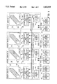
- FIG. 1 is a block diagram of a clock distribution system where a plurality of clock sources powered by separate voltage busses are synchronized across the power domain boundaries in order to simultaneously clock an equal number of equivalent circuit loads;
- FIG. 2 is a block diagram of the preferred embodiment of the Fault Tolerant Clock Distribution System
- FIG. 3 shows the Fault Tolerant Clock Distribution System when DC Power Source B or AC Power Source B has failed
- FIG. 4 is a waveform diagram which shows the Synchronized Clock Signals which supply each load, and which further illustrates how the Synchronized Clock Signal in a given power domain continues to clock its respective load upon the loss of the other Synchronized Clock Signal;
- FIG. 5 illustrates the AC power source and DC power source redundancy of the preferred embodiment
- FIG. 6 includes FIG. 6A and FIG. 6B positioned as shown, and illustrates a complete composite block diagram showing the detail of the preferred embodiment
- FIG. 7 is a block diagram of Clock Source A in Power Domain A
- FIG. 8 is a block diagram of Clock Source B in Power Domain B
- FIG. 9 is a block diagram of the method of selecting a Synchronized Clock Signal through the Primary A or the Secondary A input of the Clock Distribution Circuitry A;
- FIG. 10 is a block diagram of the first test performed by the Clock Test Circuit
- FIG. 11 is a waveform diagram of the output of Shift Register 1 is the Clock Test Circuit
- FIG. 12 is a block diagram of the second test performed by the Clock Test circuit
- FIG. 13 includes FIG. 13A and FIG. 13B positioned as shown, and is a composite diagram showing the capability of the clock distribution system to clock additional loads;
- FIG. 14 is a block diagram of the operation of the Skew Fault Detection
- FIG. 15 shows a waveform diagram of the single phase clock and the multiple phases which are produced at each load.
- FIG. 1 is a block diagram of a clock distribution system where a plurality of clock sources powered by separate voltage busses are synchronized across the power domain boundaries in order to simultaneously clock an equal number of equivalent circuit loads.
- additional clock sources may be added in additional power domains, and the original clock signals can then be synchronized with the additional clock signals to simultaneously clock as many loads as necessary (n loads) to obtain the desired assurance that power failures or clock source failures will not cause any loss of data.
- Power Domain A 10, Power Domain B 12, Power Domain C 14, and Power Domain n 16 are powered by separate DC Power Sources (DC power supplies in the preferred embodiment), and each power domain represents a completely isolated voltage bus.
- DC Power Source A 18 supplies DC voltage to the circuitry in Power Domain A
- DC Power Source B 20 supplies DC voltage to the circuitry in Power Domain B
- DC Power Source C 22 supplies DC voltage to the circuitry in Power Domain C
- DC Power Source n 24 supplies DC voltage to the circuitry in Power Domain n. Any voltage could be used to supply power to the power domains, depending on the component logic family preferred.
- the DC Power Sources supply +5 volts DC to their respective power domains.
- Each of the DC power sources is powered by an AC power source, labelled AC Power Source A 26, AC Power Source B 28, AC Power Source C 30, through AC Power Source n 32. It would be an option to reduce the number of independent AC power sources from one per power domain to at least one AC power source. This depends on the desired AC power source redundancy required for the particular application. For instance, where three power domains are utilized, it would be possible to provide AC power to the three DC power sources through only two AC power sources. In that case, two of the DC power sources would be powered by a single AC power source.
- Power Domain A 10 and Power Domain B 12 are separated by the Power Domain Boundary A/B 34
- Power Domain B and Power Domain C 14 are separated by the Power Domain Boundary B/C 36
- Power Domain n 16 would be separated from Power Domain n-1 by the Power Domain Boundary n/n-1 38, which is dependent upon the number of independent power domains chosen. These boundaries physically isolate the voltage bus of one power domain from the voltage bus of an adjacent power domain.
- clock sourcing circuitry exists which provides an oscillatory digital clock signal.
- Clock Source A 40 resides in Power Domain A
- Clock Source B 42 resides in Power Domain B
- Clock Source C 44 resides in Power Domain C
- each clock source circuit is powered by an isolated voltage bus, redundant clock source circuits will remain operative if either the AC power source or DC power source supplying voltage to the one clock source circuit fails or becomes inoperative. For example, if the power supply/power supplies comprising DC Power Source A was/were to fail, causing the clock signal of Clock Source A to stop operating, Clock Source B, Clock Source C, and all clock sources through Clock Source n 46 would be unaffected, and would continue to supply clock signal to its load.
- the system could continue operations, and the data which was lost in Load A 48 of Power Domain A will have already been preserved in Load B 50 of Power Domain B, Load C 52 of Power Domain C, and through Load n 54 of Power Domain n, since the same data that was manipulated in Load A prior to the failure of DC Power Source A was simultaneously manipulated in Load B, Load C, and through Load n. Therefore, no data loss will occur since only one of the n copies of data lost its DC power source.
- each load uses redundant power domains, redundant circuit loads, and redundant clock distribution circuitry to have the same information clocked in at the same time.
- the information or data sent to each load must be clocked at precisely the same time.
- the clock signal from Clock Source A 40 is synchronized with the clock signals from Clock Source B 42, Clock Source C 44, through Clock Source n 46. These clock signals will be referred to as Clock Signal A 56, Clock Signal B 58, Clock Signal C 60, through Clock Signal n 62.
- Synchronization of the clock signals is performed across the Power Domain Boundaries A/B 34, B/C 36, through n/n-1 38.
- the Synchronizer & Distribution Circuitry detects phase differentials between n clock signals, resynchronizes the clock signals, and distributes the Synchronized Clock Signal A 72, B 74, C 76, and n 78 to Load A 48, B 50, C 52, and n 54 respectively.
- each load comprises equivalent memory and memory control circuitry. All of the information which is clocked into one load is also being simultaneously clocked into the other loads. In this way, the loss of voltage in any power domain will only affect the information stored in that power domain's load, and the other loads will continue to store valid data. Since each load had identical information simultaneously clocked into it prior to the loss of power to one power domain, the remaining power domain's load will hold all of the previous data, plus any new data which is then clocked into it.
- FIG. 2 is a block diagram of the preferred embodiment of the Fault Tolerant Clock Distribution System.
- the power domains are labelled Power Domain A 10 and Power Domain B 12.
- Power Domain A is powered from AC Power Source A 26, and DC Power Source A 18 which consists of one or more DC power supplies.
- Power Domain B 12 is powered from AC Power Source B 28 and DC Power Source B 20.
- Clock Signal A 56 from Clock Source A 40, and Clock Signal B 58 from Power Domain B's 12 Clock Source B 42, are inputs to Synchronizer & Distribution Circuitry A 64.
- the Synchronizer & Distribution Circuitry detects phase differentials between Clock Signals A and B, adjusts Clock Signal A if the two clock signals are not properly synchronized, and distributes the Synchronized Clock Signal A 72 to Load A 48.
- Synchronized Clock Signal A consists of Clock Signal A 56 which has been adjusted to be synchronized with Clock Signal B 58.
- Synchronizer & Distribution Circuitry B 66 which detects phase differentials between Clock Signals B and A, adjusts Clock Signal B if the two clock signals are not properly synchronized, and distributes the Synchronized Clock Signal B 74 to Load B 50. Therefore, Synchronized Clock Signal B is Clock Signal B 58 which has been adjusted to be synchronized with Clock Signal A 56. By simultaneously synchronizing each clock signal with the other, Load A and Load B will be clocked at precisely the same time.
- Load A 48 and Load B 50 comprise equivalent memory and memory control circuitry. All of the information which is clocked into one load is also being simultaneously clocked into the other load. In this way, the loss of voltage in either power domain will only affect the information stored in that power domain's load, and the other load will continue to store valid data. Since each load had identical information simultaneously clocked into it prior to the loss of power to one power domain, the remaining power domain's load will hold all of the previous data, plus any new data which is then clocked into it.
- FIG. 3 shows the Fault Tolerant Clock Distribution System when DC Power Source B 20 or AC Power Source B 28 has failed.
- DC Power Source B or AC Power Source B fails, the voltage to Power Domain B 12 is no longer present on the voltage bus to supply the circuitry. None of the circuitry in Power Domain B will be operational in such a case.
- Clock Source A 40 will continue to provide clock signals to Load A 48 through Synchronization & Distribution Circuitry A 64 even though Power Domain B has failed. Since the data which was stored in Load B 50 was simultaneously stored in Load A, the data is not lost as a result of the loss of voltage to Power Domain B.
- FIG. 4 is a waveform diagram which shows the Synchronized Clock Signals which supply each load, and which further illustrates how the Synchronized Clock Signal in a given power domain continues to clock its respective load upon the loss of the other Synchronized Clock Signal.
- Clock Source A 40 would stop producing Clock Signal A 56, which would result in the loss of Synchronized Clock Signal A 72, and Load A 48 would no longer receive clock signals.
- FIG. 4 depicts the loss of Synchronized Clock Signal A 72 at the falling edge of Pulse 80, but shows that Synchronized Clock Signal B 74 will remain operative to clock Load B 50. This is because each Clock Source circuit is powered by separate DC Power Sources.
- Synchronized Clock Signal B 74 stopped functioning and Synchronized Clock Signal A 72 continued operating.
- FIG. 5 illustrates the AC power source and DC power source redundancy of the preferred embodiment.
- Power Supply A1 82 and Power Supply A2 84 reside in DC Power Source A 18, and Power Supply B1 86 and Power Supply B2 88 reside in DC Power Source B 20.
- Power Supply A1 82 connects to Power Domain A 10 through A1 +5 V 90 and A1 GND 92.
- Power Supply A2 84 connects to Power Domain A 10 through A2 +5 V 94 and A2 GND 96.
- Power Supply B1 86 connects to Power Domain B 12 through B1 +5 V 98 and B1 GND 100.
- Power Supply B2 88 connects to Power Domain B 12 through B2 +5 V 102 and B2 GND 104. If either power supply fails within DC Power Source A or DC Power Source B, the remaining power supply can supply enough current to keep the circuitry of the power domain operative. When both power supplies are operative, the power supplies share current, and both provide current to the power domain. A higher number of redundant power supplies could be used if a higher degree of DC power reliability was desired; however, dual power supplies in each DC power source provided the requisite reliability in the preferred embodiment due to the low failure rate of the power supplies implemented.
- Each of the AC power source outputs is connected to one power supply in DC Power Source A 18 and B 20.
- AC Power Source A 26 provides AC power to Power Supply A1 82 and Power Supply B1 86.
- AC Power Source B 28 provides AC power to Power Supply A2 84 and Power Supply B2 88.
- a failed AC power source will only affect one power supply in each DC power source, and the other power supply in each DC power source will remain operational. For example, if AC Power Source A 26 fails, Power Supply A1 and Power Supply B1 will lose AC input power, and will stop producing a +5 volt DC output. However, AC Power Source B 28 would still be producing AC power, and Power Supply A2 and Power Supply B2 would continue to provide the +5 volt DC voltage to Power Domain A and Power Domain B.
- AC Power Source B 28 fails, only Power Supply A2 and Power Supply B2 would stop producing +5 volts, and Power Supply A1 and Power Supply B1 would still be fully operational.
- the AC Power Source used in the preferred embodiment consists of using either utility AC power or diesel generator power, one of which will be selected through the use of an uninterruptable power source. However, it must be appreciated that any other type of AC power source would serve as well, such as motor/alternator AC power sources and the like.
- FIG. 6 includes FIG. 6A and FIG. 6B positioned as shown, and illustrates a complete composite block diagram showing the detail of the preferred embodiment.
- each power domain consists of clock sourcing capabilities, synchronization and distribution circuitry, and recipient load circuitry.
- FIG. 6 shows that two Clock Signals exist in each Clock Source A 40 and B 42.
- Clock Source A consists of Primary Clock Signal Drive A 106 and Redundant Clock Signal Drive A 108
- Clock Source B consists of Primary Clock Signal Drive B 110 and Redundant Clock Signal Drive B 112.
- the Primary Clock Signal Drives provide the default clock signal
- the Redundant Clock Signal Drives provide the clock signal which can be selected upon a failure of the Primary Clock Signal Drive.
- FIG. 7 is a block diagram of Clock Source A 40 in Power Domain A 10.
- the Primary Clock Signal Drive A 106 contains Oscillator A1 114 and Clock Shape A1 116, and the Redundant Clock Signal Drive A 108 contains Oscillator A2 118 and Clock Shape A2 120.
- Each oscillator produces a digital clock signal which is connected to the Clock Shape circuitry.
- the Clock Shape circuitry is included to produce a symmetric clock pulse with a 50% duty cycle, which creates more pronounced triggering edges, and allows inverted clock signals to be utilized.
- Clock Signals A1 122 and A2 124 of Clock Shape A1 116 and A2 120 are the clock signals of which one will be synchronized with a clock signal from Power Domain B 12.
- Clock signal A1 122 and Clock Signal A2 124 are species of the generic Clock Signal A 56 depicted in FIGS. 1, 2, and 3.
- FIG. 8 is a block diagram of Clock Source B 42 in Power Domain B 12.
- the Primary Clock Signal Drive B 110 contains Oscillator B1 126 and Clock Shape B1 128, and the Redundant Clock Signal Drive B 112 contains Oscillator B2 130 and Clock Shape B2 132.
- the function of Clock Source B 42 is analogous to that of Clock Source A 40 described above.
- Clock Signals B1 134 and B2 136 of Clock Shape B1 128 and B2 132 are the clock signals of which one will be synchronized with a clock signal from Power Domain A 10.
- Clock signal B1 134 and Clock Signal B2 136 are species of the generic Clock Signal B 58 depicted in FIGS. 1, 2, and 3.
- Clock Signals A1 122, A2 124, B1 134, and B2 136 are connected to Synchronizers A1 138, A2 140, B1 142, and B2 144 respectively.
- a Synchronizer will resynchronize its associated Clock Signal with another Clock Signal that clocks the load in the other power domain.
- the synchronizers resynchronize the Clock Signal upon a request from a phase detector, which monitors the phase differential between two given Clock Signals.
- the four Clock Signals, Clock Signal A1 138, Clock Signal A2 124, Clock Signal B1 134, and Clock Signal B2 136 are synchronized with each other in various combinations of "clock pairs".
- a clock pair is a synchronized pair of Clock Signals, where each of the two resulting Synchronized Clock Signals clocks a load in one of the two power domains. Therefore, two of the four Clock Signals are selected as the "active" signals, and each will clock one of the loads in a power domain. These two clock signals are synchronized with each other before clocking its respective load so that the loads are guaranteed to perform functions at precisely the same time. The remaining two Clock Signals (the two of the four which were not selected as the active signals) are "inactive" in the sense that they will not be currently clocking a load.
- Synchronized Clock Signals comprise four sets of clock pairs: 1) Synchronized Clock Signal A1-A2 146 and Synchronized Clock Signal A2-A1 150, 2) Synchronized Clock Signal A1-B1 148 and Synchronized Clock Signal B1-A1 156, 3) Synchronized Clock Signal A2-B2 152 and Synchronized Clock Signal B2-A2 160, and 4) Synchronized Clock Signal B1-B2 154 and Synchronized Clock Signal B2-B1 158.
- two of these clock pairs comprise pairs of Synchronized Clock Signals within the same power domain: Synchronized Clock Signal A1-A2 and Synchronized Clock Signal A2-A1, and Synchronized Clock Signal B1-B2 and Synchronized Clock Signal B2-B1.
- the reason for providing these clock pairs is to allow for the replacement of circuitry within one power domain while allowing the circuit loads associated with that power domain to continue to be clocked by the circuitry of the other power domain. For example, if the circuitry within Clock Source B 42 was to fail, Synchronized Clock Signal A2-A1 150 could clock Load B 50.
- Clock Source B 42 was on a separate printed circuit board, as in the preferred embodiment, this board can be replaced without having to discontinue clock signals to Load B 50.
- this board can be replaced without having to discontinue clock signals to Load B 50.
- Synchronized Clock Signal A1-A2 146 would clock Load A 48 by itself, and Synchronized Clock Signal A2-A1 150 would not be used.
- Synchronized Clock Signal A2-A1 could have been used as a redundant signal for Load A 48, it was not used as such in the preferred embodiment because it was determined that Power Domain B 12 would always be used, and it would be powered up immediately following the application of power to Power Domain A 10.
- the very short time between application of power to Power Domain A and the application of power to Power Domain B did not justify the need for supplying Synchronized Clock Signal A2-A1 150 to the Secondary A 198 input for redundancy. Therefore, although the active clock pair will be the clock pair comprising Synchronized Clock Signal A1-A2 146 and Synchronized Clock Signal A2-A1 150 at system power up, only Synchronized Clock Signal A1-A2 146 will be clocking Load A 48. When Power Domain B 12 is then powered up, the system will choose a Clock Signal from each Power Domain to clock its respective load.
- Phase Detector A1-A2/A2-A1 164 monitors for phase differences between Clock Signal A1 122 and Clock Signal A2 124. If Phase Detector A1-A2/A2-A1 establishes that Clock Signal A1 is leading Clock Signal A2, it will send a signal to Synchronizer A1 138 to delay for a short time to resynchronize Clock Signal A1 with Clock Signal A2. If Phase Detector A1-A2/A2-A1 determines that Clock Signal A2 is leading Clock Signal A1, it will send a signal to Synchronizer A2 140 to delay for a short time to resynchronize Clock Signal A2 with Clock Signal A1.
- Phase Detector A1-B1/B1-A1 166 monitors Clock Signal A1 and Clock Signal A2, and sends a signal to Synchronizer A1 138 or Synchronizer B1 142 if necessary to delay the clock signal which is leading the other.
- Phase Detector B1-B2/B2-B1 168 monitors Clock Signal B1 and Clock Signal B2, and sends a signal to Synchronizer B1 142 or Synchronizer B2 144 if necessary to delay the clock signal which is leading the other.
- Phase Detector A2-B2/B2-A2 170 monitors Clock Signal A2 and Clock Signal B2, and sends a signal to Synchronizer A2 140 or Synchronizer B2 144 if necessary to delay the clock signal which is leading the other.
- a clock pair is a set of two Clock Signals which have been synchronized with each other to produce complementary Synchronized Clock Signals. Therefore, one clock pair consists of two complementary clock signals.
- the pair of Synchronized Clock Signals including Synchronized Clock Signal A1-B1 148 and Synchronized Clock Signal B1-A1 156 are referred to as the A1-B1/B1-A1 clock pair.
- four clock pairs comprising four Synchronized Clock Signals and their complements (eight Synchronized Clock Signals total) are produced by the four sets of Clock Signals.
- FIG. 6 shows the four sets of clock pairs at the outputs of the synchronizers.
- the four sets of clock pairs are A1-A2/A2-A1 (comprising Synchronized Clock Signals A1-A2 146 and A2-A1 150), A1-B1/B1A1 (comprising Synchronized Clock Signals A1-B1 148 and B1-A1 156), B1-B2/B2-B1 (comprising Synchronized Clock Signals B1-B2 154 and B2-B1 158), and A2-B2/B2-A2 (comprising Synchronized Clock Signals A2-B2 152 and B2-A2 160).
- A1-A2/A2-A1 comprising Synchronized Clock Signals A1-A2 146 and A2-A1 150
- A1-B1/B1A1 comprising Synchronized Clock Signals A1-B1 148 and B1-A1 156
- B1-B2/B2-B1 comprising Synchronized Clock Signals B1-B2 154 and B2-
- All four of the clock pairs are available at the output of the synchronizers whenever voltage is supplied to both power domains. Therefore, there must be a method of selecting a clock pair to distribute the clock signals to the loads in the power domains. This is performed via the Select #1 172, Select #2 174, Select #3 176, and Select #4 178 circuits. These circuits provide a multiplexer-type function, and allow a specified clock pair to pass to Clock Distribution Circuitry A 162 and Clock Distribution Circuitry B 180 at the direction of the Network Interface Modules (NIM) A 182 and B 184.
- the NIMs provides a user interface for clock pair changes desired by the user. Automatic clock pair changes are also possible when error detection circuitry indicates clock signal errors to the NIMs.
- the error detection circuitry of the present invention includes Skew Fault Detection A 186 and B 188. This error detection circuit is discussed in a later portion of this description.
- NIM circuits such as NIM A 182 and B 184, reside in each power domain which houses a Clock Source, such as Clock Source A 40 and B 42. In other words, a NIM will not be present in power domains which only house additional circuit loads. The capability of the clock distribution system to provide clock signals to additional loads is described in a later portion of this description.
- One of the two NIM circuits acts as a master controller, while the other acts as a slave controller.
- Three control signals are provided from the master NIM to each of the Select circuits to enable one of the three Synchronized Clock Signals.
- a SYNC signal is a periodic pulse which is sent to the synchronization circuitry to determine whether or not the two Clock Signals are synchronized.
- a SYNC signal is created at the Primary Clock Signal Drive A 106 and at the Redundant Clock Signal Drive A 108 of Clock Source A 40.
- a SYNC signal is also created at the Primary Clock Signal Drive B 110 and at the Redundant Clock Signal Drive B 112 of Clock Source B 42.
- Synchronizers A1 138, A2 140, B1 142, and B2 144 use these SYNC signals to help synchronize the Clock Signals.
- the SYNC signals are also sent to each load in the system to produce multiple phases of the clock signal, which in turn are used because certain circuits within each load require offset phases for timing purposes.
- the SYNC signal which is selected will always be derived from the Clock Signals which comprise the selected clock pair.
- clock pair A1-B1/B1-A1 comprising Synchronized Clock Signals A1-B1 148 and B1-A1 156) is selected by Select #1 179 and Select #3 176 respectively to clock Load A 48 and Load B 50
- a SYNC signal which is derived from the Primary Clock Signal Drive A 106 in Clock Source A 40 is sent to Synchronizer A1 138 and Load A 48
- a SYNC signal which is derived from the Primary Clock Signal Drive B 110 in Clock Source B 49 is sent to Synchronizer B1 149 and Load B 50.
- SYNC signals are only required as a result of the specific synchronizer utilized in the preferred embodiment, and due to the preferred use of a multiple phase clock signal at the loads. Many different types of synchronizers are known in the prior art, and the specific SYNC signal used in the preferred embodiment would not be required in those synchronizers.
- each of the Select circuits There are six signals sent from the master and slave NIM to each of the Select circuits (24 signals total) to enable the desired Synchronized Clock Signal and SYNC signal to pass to Clock Distribution Circuitry A 162 and Clock Distribution Circuitry B 180. Any type of selection circuitry could be used to select the desired signals, and in the preferred embodiment each of the 24 signals is ANDed with one of the 24 Clock Signals or SYNC signals to allow the desired signal to pass to the Clock Distribution Circuitry A 162 and B 180.
- the master NIM A 182 or B 184 selects particular signals depending upon whether an error has occurred, or whether a request was made by User Interface A 190 or B 192 to switch to a new clock pair.
- FIG. 6 shows that some of the Synchronized Clock Signals are connected to more than one Select circuit.
- Synchronized Clock Signal A1-B1 148 and its complement Synchronized Clock Signal B1-A1 156, and Synchronized Clock Signal A2-B2 152 and its complement Synchronized Clock Signal B2-A2 160 are each connected to one Select circuit within its power domain, and to one Select circuit in the other power domain.
- Synchronized Clock Signal A1-B1 is connected to Select #1 172 and Select #4 178
- Synchronized Clock Signal A2-B2 is connected to Select #1 and Select #4
- Synchronized Clock Signal B1-A1 is connected to Select #2 174 and Select #3 176
- Synchronized Clock Signal B2-A2 is connected to Select #2 and Select #3. This is to provide alternate routes for Clock Signals which are synchronized with a Clock Signal from the other power domain.
- the Clock Distribution Circuitry A 162 or B 180 will recognize the loss of the Synchronized Clock Signal to its Primary A 194 or B 196 input, and will automatically switch to the alternate Select circuit which will supply the Synchronized Clock Signal to the Secondary A 198 or Secondary B 200 input. For example, if Select #1 became unavailable or failed for any reason, Clock Distribution Circuitry A's 162 Primary A 194 input would recognize the loss of the Synchronized Clock Signal A1-B1 148 input, and would switch so that the Secondary A 198 input which is connected to Select #4 178 would receive the Synchronized Clock Signal A1-B1 148.
- FIG. 9 is a block diagram of the method of selecting a Synchronized Clock Signal through the Primary A 194 or the Secondary A 198 input of the Clock Distribution Circuitry A 162.
- Clock Distribution Circuitry A will be used in this example, but the same description applies to Clock Distribution Circuitry B 180 or other additional Clock Distribution Circuits.
- Select #1 172 and Select #4 178 are connected to the Primary A 194 and Secondary A 198 inputs respectively of Clock Distribution Circuitry A.
- Select #4 is the alternate Select circuit for the Synchronized Clock Signal A1-B1 148.
- the Select circuits each provide the Synchronized Clock Signal and a SYNC signal to the Clock Distribution Circuitry.
- the SYNC signals were briefly discussed previously.
- a SYNC signal is generated by the same oscillators that generate the clock signals, and a SYNC signal has a waveform in which a pulse occurs every eighth cycle of a Synchronized Clock Signal pulse.
- SYNC signals labelled SYNC A1-B1 202 in this example, are connected through the Primary A 194 and Secondary A 198 inputs to the Clock Test Circuit 204.
- Synchronized Clock Signal A1-B1 148 is connected through the Primary A input and Select #1 172 to the Multiplexer 206, and is also connected through the Secondary A input and Select #4 178 to the Multiplexer.
- Test Circuit Output 208 is a control signal connected to the Multiplexer to indicate which input path of the Synchronized Clock Signal A1-B1 148 should be selected to drive the circuit loads.
- the selected input path at the Multiplexer output is driven to these circuit loads through the Fanout Drivers 210.
- Synchronized Clock Signal A1-B1 148 at the Primary A 194 input is the default signal which is selected by the Multiplexer 206 in response to the Clock Test Circuit 204 upon power up of Power Domain A 10, or upon a reset of the Clock Distribution Circuitry A 162.
- the Clock Test Circuit will continue to indicate to the Multiplexer 206 to select Synchronized Clock Signal A1-B1 148 from the Primary A 194 input until the Clock Test Circuit determines that a problem with Synchronized Clock Signal A1-B1 has occurred.
- the Clock Test Circuit will switch the logic state of the Test Circuit Output 208 so that the Multiplexer 206 will select Synchronized Clock Signal A1-B1 148 from the Secondary A 198 input to drive the circuit loads. Therefore, if Synchronized Clock Signal A1-B1 148 becomes unavailable or the Select #1 172 circuit fails, the Synchronized Clock Signal A1-B1 148 will be selected at Select #4 178, and the Clock Test Circuit 204 will select the Secondary A 198 input to drive the circuit loads.
- FIG. 10 is a block diagram of the first test performed by the Clock Test Circuit 204. This test is performed for each of the Synchronized Clock Signals at the Primary A 194 and Secondary A 198 inputs, but will only be described with respect to Synchronized Clock Signal A1-B1 148. It should be noted that this test is performed at both the Primary A 194 and Secondary A 198 inputs, and the Synchronized Clock Signal used will depend upon which Synchronized Clock Signal was chosen by the Select circuits.
- a detected error of the first test occurs when the Presence Detector 214 determines that each phase produced by Shift Register 1 216 occurs at a predetermined time relative to the SYNC A1-B1 202 signal.
- the Synchronized Clock Signal A1-B1 148 is the clock signal for the logic in both the Shift Register 1 216 and the Presence Detector 214.
- the Shift Register Output 208 consists of eight shifted outputs. An error on Error 1 202 will cause the Test Circuit Output 208 to switch logic states, which will indicate to the Multiplexer 206 to select Synchronized Clock Signal A1-B1 148 from the Secondary A 198 input to drive the circuit loads.
- FIG. 11 is a waveform diagram of the output of Shift Register 1 216 in the Clock Test Circuit 204.
- the Shift Register Output 218 of Shift Register 1 216 consists of eight shifted outputs, labelled Shift Output 1 220, Shift Output 2 222, Shift Output 3 224, Shift Output 4 226, Shift Output 5 228, Shift Output 6 230, Shift Output 7 232, and Shift Output 8 234.
- These shifted outputs are then compared to the SYNC A1-B1 202 to determine whether the particular shifted output is present when it should be, and is absent when it should be.
- Shift Output 1 220 or Shift Output 8 234 be a logic high when the SYNC A1-B1 202 is a logic high. Accordingly, Shift Output 2 through Shift Output 7 must be a logic low when the SYNC A1-B1 202 is a logic high.
- the Presence Detector 214 performs this comparison, and this type of comparison is obvious to one skilled in the art.
- Presence Detector determines that Shift Output 1 or Shift Output 8 is absent when it should be present, this will indicate that the SYNC A1-B1 202 is not present at the Primary A 194 input, and the Error 1 212 will cause the Clock Test Circuit 204 to switch the logic state of the Test Circuit Output 208 so that the Multiplexer 206 will select Synchronized Clock Signal A1-B1 148 from the Secondary A 198 input to drive the circuit loads.
- FIG. 12 is a block diagram of the second test performed by the Clock Test Circuit 204. This test compares the Shift Register Output 218 of Shift Register 1 216 to the Shift Register Output 236 of Shift Register 2 238.
- the Presence Comparators 1 240 and 2 242 perform the comparison, and produces the signal Error 2 244 or Error 3 246 respectively upon determining that an error has occurred.
- Select #1 172 and Select #4 178 transmit the SYNC A1-B1 202 signal and the Synchronized Clock Signal A1-B1 148 to Shift Register 1 216 and Shift Register 2 238 respectively.
- Shift Register 1 accepts the SYNC A1-B1 signal and the Synchronized Clock Signal A1-B1 at the Primary A 194 input
- Shift Register 2 accepts the SYNC A1-B1 signal and the Synchronized Clock Signal A1-B1 at the Secondary A 198 input.
- Presence Comparator 1 240 and Presence Comparator 2 242 each input Shift Register Output 1 218 and Shift Register Output 2 236, which each consist of eight shifted outputs.
- Synchronized Clock Signal A1-B1 148 from Select #4 178 clocks Presence Comparator 1 240
- Synchronized Clock Signal A1-B1 148 from Select #1 172 clocks Presence Comparator 2 242.
- the Presence Comparators compare each of the eight shifted outputs to each other. For instance, Shift Output 2 222 (shown in FIG. 11) of Shift Register 1 216 will be compared to Shift Output 2 (not shown) of Shift Register 2 238. If the Presence Comparator determines that one is absent when the other is present, it will issue the associated Error 2 244 signal or the Error 3 246 signal. The Presence Comparators are able to do this because Presence Comparator 1 240 receives its SYNC A1-B1 202 signal from the Primary A 194 input, but is clocked by the Synchronous Clock Signal A1-B1 148 associated with the Secondary A 198 input.
- Presence Comparator 2 242 receives its SYNC A1-B1 202 signal from the Secondary A 198 input, but is clocked by the Synchronous Clock Signal A1-B1 148 associated with the Primary A 194 input. Therefore, if the SYNC A1-B1 202 from Select #1 172 fails to reach the Primary A 194 input, the Presence Comparator 1 240 will detect that the shifted output from Shift Register 1 216 is no longer present, since Presence Comparator 1 will continue to be clocked by the Synchronous Clock Signal A1-B1 148 from the Secondary A 198 input. The same holds true by analogy if the SYNC A1-B1 202 from Select #4 178 fails to reach the Secondary A 198 input. The comparison performed by the Presence Comparators 1 240 and 2 242 is simply a signal-to-signal comparison so that it would be obvious to one skilled in the art.
- clock signals are used only for clock signals which are synchronized with signals from the other power domain. Where clock signals are synchronized with other clock signals from the same power domain, it is possible that the other power domain has not even had voltage applied to it yet, and therefore the Select circuitry from that power domain would not be active. Furthermore, since it is desirable to use Clock Signals from different power domains, two Clock Signals from the same power domain will comprise the active clock pair only where one circuit load is to be utilized, where the system is in initial power up stage, or where multiple oscillators have failed.
- FIG. 13 includes FIG. 13A and FIG. 13B positioned as shown, and is a composite diagram showing the capability of the clock distribution system to clock additional loads.
- the Clock Module 248 represents the portion of the entire Fault Tolerant Clock Distribution System which has thus far been described.
- additional loads such as Circuit Load Group #2 250 through Circuit Load Group #n 252 may be clocked by the same clock distribution system.
- Each additional load is connected in parallel with the first load of Circuit Load Group #1 254.
- Each Primary A 194 in FIG. 13 is connected to the output of Select #1 172.
- Each Secondary A 198 in FIG. 13 is connected to the output of Select #4 178.
- Each Primary B 196 in FIG. 13 is connected to the output of Select #3 176.
- Clock Distribution Circuitry A 162 and Clock Distribution Circuitry B 180 provide two major functions. The first is to provide redundant input selection so that a valid clock signal is recognized even in the event that one of the Select circuits fail. For instance, if Select #1 172 were to fail so that no clock signal input was present at the Primary A 194 input of Clock Distribution Circuitry A 162, Synchronized Clock Signal A1-B1 148 would be present at Secondary A 198 of Clock Distribution Circuitry A through the Select #4 178 circuit. The Clock Distribution Circuitry A must recognize the loss of clock signal input at the Primary A input, and automatically use the clock signal input at the Secondary A input.
- the second major function of the Clock Distribution Circuitry A 162 and B 180 is to provide the fan-out capability to the respective circuit loads.
- the present invention incorporates an error detection circuit in order to detect synchronization errors, and provides means to switch to operational oscillators.
- the error detection circuit of the present invention is the Skew Fault Detection A 186 and B 188. This error detection circuit resides in Power Domain A 10 and, Power Domain B 12 since those power domains comprise the Clock Module 248. No clock error detection circuits are required in any other power domains which exist only to house additional circuit load groups.
- FIG. 14 is a block diagram of the operation of the Skew Fault Detection.
- a skew fault occurs when the two clock signals which are being monitored are out of phase to the extent that the synchronizers cannot successfully resynchronize them.
- the Skew Fault Detection A 186 circuitry detects inadmissible phase differentials between the two clock signals, detects which clock signal is faster, and disables the faster of the two.
- the operation of the Skew Fault Detection A 186 will be described through explanation of skew fault monitoring of Synchronizers A1 138 and B1 142. However, it should be recognized that skew fault monitoring occurs for multiple pairs of synchronizers in the system, and the operation of skew fault monitoring for the other pairs of synchronizers is analogous to the forthcoming description.
- the inputs of the Skew Fault Detection A 186 are the Synchronized Clock Signals A1-B1 148 and B1-A1 156 which are generated by Synchronizer A1 138 and Synchronizer B1 142 respectively.
- Clock Signal A1 122 and Clock Signal B1 134 are monitored by Phase Detector A1-B1/B1-A1 166, which in turn sends resynchronization requests to the synchronizers if the two Clock Signals are not synchronized.
- Synchronizer A1 138 will delay Clock Signal A1 122 for a short time if Clock Signal A1 is oscillating faster than Clock Signal B1 134.
- Synchronizer B1 142 will delay Clock Signal B1 134 for a short time if Clock Signal B1 is oscillating faster than Clock Signal A1.
- the Skew Fault Detection A 186 ensures that Synchronizers A1 138 and B1 142 have successfully resynchronized the out-of-phase clock signals. Therefore, the Skew Fault Detection A ensures that the Synchronizers are working properly and that they can maintain synchronization of the two clock signals.
- Skew Fault Detection is desirable in a multiple oscillator clock distribution system so that an operational clock pair may be selected if the currently active clock pair is no longer staying properly synchronized.
- the Skew Fault Detection circuitry establishes that the clock signals which are outputted by Synchronizer A1 138 and Synchronizer B1 142 are not properly synchronized, a skew fault will occur.
- This error signal is sent to the Network Interface Module A (NIM A) 182, and a skew fault error message is sent to the System Control Facility (SCF) 256.
- the NIM A will disable both Synchronized Clock Signal A1-B1 148 and Synchronized Clock Signal B1-A1 156, and will enable a new pair of synchronized clock signals to drive the circuit loads through the Select #1 172 and Select #3 176 circuits.
- the selection of a new clock pair is done either automatically, or manually through the User Interface A 190, depending on which mode the NIM A has been set to.
- multiple skew detectors are used, and a voting scheme is used which requires at least two skew faults to be present before a skew fault will be acknowledged.
- a voting scheme is used which requires at least two skew faults to be present before a skew fault will be acknowledged.
- the clock signals which are distributed to the circuit loads in this design are "single phase” clock signals, i.e., only a single “pulse train” is provided. It may be desirable to provide multiple phases at the load so that latches, registers, and other timed activities can be set or cleared at the occurrence of a particular pulse of the clock signal relative to another pulse of the clock signal. For example, during a period of four pulses of a clock signal, it may be desired to set one level of registers on the first pulse of the four-period interval, and to set another level of registers on the third pulse of the four-period interval. To accomplish this, a clock distribution system may generate four phases at the clock source circuitry, and distribute all four phases to the load circuitry.
- the present invention does not generate multiple phases at the clock source circuitry however. Due to the use of multiple oscillators for purposes of redundancy, it would be complicated and problematic to detect phase differentials and to synchronize multiple phases of multiple oscillators. For example, the present invention utilizes four oscillators which are simultaneously synchronized, and if a four-phase clock were generated from the selected Synchronized Clock Signal, then four signals must be controlled during distribution to the circuit loads. In order to avoid this situation, the clock distribution system of the preferred embodiment does not generate multiple phases at the clock source circuitry, but rather generates multiple phase enables from the single phase clock at the load itself. In this way, only one phase of each Clock Signal A1 122, A2 124, B1 134, and B2 136 requires synchronization and distribution, and the circuit loads themselves are enabled to receive the single phase clock.
- FIG. 15 shows a waveform diagram of the single phase clock and the multiple phases which are produced at each circuit load. As seen from the diagram, four phases are constructed at the load from the single phase generic Clock Signal 258.
- Each of the Generated Clock Phases 1 260, 2 262, 3 264, and 4 266 consists of a high pulse of duration equal to one period of the Clock Signal 258. The pulses repeat every fourth pulse of the Clock Signal.
- Generated Clock Phase 1 260 switches to an active high at the rising edge of Pulse 1 268 of the Clock Signal.
- Generated Clock Phase 2 262 switches to an active high at the rising edge of Pulse 2 270 of the Clock Signal.
- Generated Clock Phase 3 264 switches to an active high at the rising edge of Pulse 3 272 of the Clock Signal.
- Generated Clock Phase 4 266 switches to an active high at the rising edge of Pulse 4 274 of the Clock Signal.
- the use of the four-phase clock allows particular circuits within each load to be clocked at specific pulses of the single phase Clock Signal 2B8.
- the single phase clock provides a four phase clock at the circuit loads using multiple phase enables, see copending Patent Application "Multiple Interval Single Phase Clock", Serial No. 08/173,733, and assigned to the assignee of this application.
Abstract
Description
Claims (21)
Priority Applications (2)
| Application Number | Priority Date | Filing Date | Title |
|---|---|---|---|
| US08/172,661 US5422915A (en) | 1993-12-23 | 1993-12-23 | Fault tolerant clock distribution system |
| US08/180,896 US5574753A (en) | 1993-12-23 | 1994-01-12 | Glitch free clock start/stop control circuit for outputting a single clock signal and a single sync signal from a plurality of sync signal inputs and a plurality of clock signal inputs |
Applications Claiming Priority (1)
| Application Number | Priority Date | Filing Date | Title |
|---|---|---|---|
| US08/172,661 US5422915A (en) | 1993-12-23 | 1993-12-23 | Fault tolerant clock distribution system |
Related Child Applications (1)
| Application Number | Title | Priority Date | Filing Date |
|---|---|---|---|
| US08/180,896 Continuation-In-Part US5574753A (en) | 1993-12-23 | 1994-01-12 | Glitch free clock start/stop control circuit for outputting a single clock signal and a single sync signal from a plurality of sync signal inputs and a plurality of clock signal inputs |
Publications (1)
| Publication Number | Publication Date |
|---|---|
| US5422915A true US5422915A (en) | 1995-06-06 |
Family
ID=22628657
Family Applications (1)
| Application Number | Title | Priority Date | Filing Date |
|---|---|---|---|
| US08/172,661 Expired - Lifetime US5422915A (en) | 1993-12-23 | 1993-12-23 | Fault tolerant clock distribution system |
Country Status (1)
| Country | Link |
|---|---|
| US (1) | US5422915A (en) |
Cited By (41)
| Publication number | Priority date | Publication date | Assignee | Title |
|---|---|---|---|---|
| US5515403A (en) * | 1994-06-21 | 1996-05-07 | Dsc Communications Corporation | Apparatus and method for clock alignment and switching |
| US5530726A (en) * | 1993-06-18 | 1996-06-25 | Nec Corporation | Method and apparatus for switching of duplexed clock system |
| US5568097A (en) * | 1995-09-25 | 1996-10-22 | International Business Machines Inc. | Ultra high availability clock chip |
| US5574753A (en) * | 1993-12-23 | 1996-11-12 | Unisys Corporation | Glitch free clock start/stop control circuit for outputting a single clock signal and a single sync signal from a plurality of sync signal inputs and a plurality of clock signal inputs |
| US5615177A (en) * | 1994-06-08 | 1997-03-25 | Kabushiki Kaisha Toshiba | Hybrid-synchronous type clock synchronizing apparatus of which dominant gain greater than sum of other gains, network therewith, and clock synchronizing method thereof |
| US5619158A (en) * | 1995-08-18 | 1997-04-08 | International Business Machines Corp. | Hierarchical clocking system using adaptive feedback |
| US5642069A (en) * | 1994-04-26 | 1997-06-24 | Unisys Corporation | Clock signal loss detection and recovery apparatus in multiple clock signal system |
| US5670856A (en) * | 1994-11-07 | 1997-09-23 | Alliedsignal Inc. | Fault tolerant controller arrangement for electric motor driven apparatus |
| US5758132A (en) * | 1995-03-29 | 1998-05-26 | Telefonaktiebolaget Lm Ericsson | Clock control system and method using circuitry operating at lower clock frequency for selecting and synchronizing the switching of higher frequency clock signals |
| US5774705A (en) * | 1995-09-28 | 1998-06-30 | Emc Corporation | Dual oscillator clock pulse generator |
| US5831805A (en) * | 1997-02-13 | 1998-11-03 | Sony Corporation | Local power failure detection and clock disabling circuit |
| US5852640A (en) * | 1995-06-26 | 1998-12-22 | Kliza; Phillip S. | Clock distribution apparatus with current sensed skew cancelling |
| US5852728A (en) * | 1995-01-12 | 1998-12-22 | Hitachi, Ltd. | Uninterruptible clock supply apparatus for fault tolerant computer system |
| US5886557A (en) * | 1996-06-28 | 1999-03-23 | Emc Corporation | Redundant clock signal generating circuitry |
| US5966522A (en) * | 1997-03-28 | 1999-10-12 | International Business Machines Corporation | Multi-phase clock distribution method and system for complex integrated-circuit devices |
| US6055362A (en) * | 1996-03-29 | 2000-04-25 | Bull Hn Information Systems Inc. | Apparatus for phase synchronizing clock signals in a fully redundant computer system |
| US6125465A (en) * | 1998-01-09 | 2000-09-26 | International Business Machines Corporation | Isolation/removal of faults during LBIST testing |
| WO2000070460A1 (en) * | 1999-05-19 | 2000-11-23 | Sun Microsystems, Inc. | Redundant synchronous clock distribution for computer systems |
| US6204732B1 (en) | 1999-02-09 | 2001-03-20 | Eci Telecom Ltd | Apparatus for clock signal distribution, with transparent switching capability between two clock distribution units |
| US6285687B1 (en) * | 1996-12-26 | 2001-09-04 | Alcatel Usa Sourcing, L.P. | Timing system and method for distributing a timing signal |
| US6462592B1 (en) * | 1999-09-07 | 2002-10-08 | Lg Electronics Inc. | Clock signal converting apparatus of a transmission system |
| US6467044B1 (en) | 1999-10-20 | 2002-10-15 | International Business Machines Corporation | On-board clock-control templates for testing integrated circuits |
| US20020163370A1 (en) * | 1999-10-04 | 2002-11-07 | Martin Peller | Operating method for a data bus |
| US6538516B2 (en) * | 2001-05-17 | 2003-03-25 | Fairchild Semiconductor Corporation | System and method for synchronizing multiple phase-lock loops or other synchronizable oscillators without using a master clock signal |
| US20030210082A1 (en) * | 2002-05-07 | 2003-11-13 | Hughes Rodney A. | Generation of synchronized clocks to multiple locations in a system |
| US6720815B2 (en) * | 1998-11-10 | 2004-04-13 | Renesas Technology Corp. | Phase adjustor for semiconductor integrated circuit |
| US6731154B2 (en) * | 2002-05-01 | 2004-05-04 | International Business Machines Corporation | Global voltage buffer for voltage islands |
| US20040120343A1 (en) * | 2002-09-06 | 2004-06-24 | Kabushiki Kaisha Toshiba | Asynchronous serial data receiver for packet transfer |
| US20040119516A1 (en) * | 2002-07-23 | 2004-06-24 | Lg Electronics Inc. | Multi clock deciding system |
| US6757350B1 (en) | 1999-06-12 | 2004-06-29 | Cisco Technology, Inc. | Redundant clock generation and distribution |
| US6832331B1 (en) * | 2000-02-25 | 2004-12-14 | Telica, Inc. | Fault tolerant mastership system and method |
| US6833634B1 (en) * | 2001-01-04 | 2004-12-21 | 3Pardata, Inc. | Disk enclosure with multiple power domains |
| US20050200394A1 (en) * | 2004-03-10 | 2005-09-15 | Brad Underwood | Systems and methods for providing distributed control signal redundancy among electronic circuits |
| US7036033B1 (en) * | 2001-01-04 | 2006-04-25 | 3Pardata, Inc. | Disk enclosure with multiplexers for connecting 12C buses in multiple power domains |
| US20070127615A1 (en) * | 2005-12-06 | 2007-06-07 | Applied Materials, Inc. | DC technique for eliminating phase ambiguity in clocking signals |
| US7233274B1 (en) | 2005-12-20 | 2007-06-19 | Impinj, Inc. | Capacitive level shifting for analog signal processing |
| US7581131B1 (en) * | 2005-05-09 | 2009-08-25 | National Semiconductor Corporation | Method and system for balancing clock trees in a multi-voltage synchronous digital environment |
| US20100090738A1 (en) * | 2008-10-13 | 2010-04-15 | Wei-Pin Changchein | Circuit and Method for Clock Skew Compensation in Voltage Scaling |
| US20120173916A1 (en) * | 2007-08-23 | 2012-07-05 | Garth Dylan Wiebe | Apparatus and Method for Redundant and Spread Spectrum Clocking |
| CN113767340A (en) * | 2021-08-02 | 2021-12-07 | 华为技术有限公司 | Control device, electronic control system, and vehicle |
| US11650620B2 (en) | 2019-05-22 | 2023-05-16 | Vit Tall Llc | Multi-clock synchronization in power grids |
Citations (7)
| Publication number | Priority date | Publication date | Assignee | Title |
|---|---|---|---|---|
| US4254492A (en) * | 1979-04-02 | 1981-03-03 | Rockwell International Corporation | Redundant clock system utilizing nonsynchronous oscillators |
| US4412342A (en) * | 1981-12-18 | 1983-10-25 | Gte Automatic Electric Labs Inc. | Clock synchronization system |
| US4644498A (en) * | 1983-04-04 | 1987-02-17 | General Electric Company | Fault-tolerant real time clock |
| US4707142A (en) * | 1986-12-05 | 1987-11-17 | Westinghouse Electric Corp. | Master clock system for a parallel variable speed constant frequency power system |
| US4754164A (en) * | 1984-06-30 | 1988-06-28 | Unisys Corp. | Method for providing automatic clock de-skewing on a circuit board |
| US4882738A (en) * | 1987-06-25 | 1989-11-21 | Nec Corporation | Clock control system |
| US5036528A (en) * | 1990-01-29 | 1991-07-30 | Tandem Computers Incorporated | Self-calibrating clock synchronization system |
-
1993
- 1993-12-23 US US08/172,661 patent/US5422915A/en not_active Expired - Lifetime
Patent Citations (7)
| Publication number | Priority date | Publication date | Assignee | Title |
|---|---|---|---|---|
| US4254492A (en) * | 1979-04-02 | 1981-03-03 | Rockwell International Corporation | Redundant clock system utilizing nonsynchronous oscillators |
| US4412342A (en) * | 1981-12-18 | 1983-10-25 | Gte Automatic Electric Labs Inc. | Clock synchronization system |
| US4644498A (en) * | 1983-04-04 | 1987-02-17 | General Electric Company | Fault-tolerant real time clock |
| US4754164A (en) * | 1984-06-30 | 1988-06-28 | Unisys Corp. | Method for providing automatic clock de-skewing on a circuit board |
| US4707142A (en) * | 1986-12-05 | 1987-11-17 | Westinghouse Electric Corp. | Master clock system for a parallel variable speed constant frequency power system |
| US4882738A (en) * | 1987-06-25 | 1989-11-21 | Nec Corporation | Clock control system |
| US5036528A (en) * | 1990-01-29 | 1991-07-30 | Tandem Computers Incorporated | Self-calibrating clock synchronization system |
Cited By (58)
| Publication number | Priority date | Publication date | Assignee | Title |
|---|---|---|---|---|
| US5530726A (en) * | 1993-06-18 | 1996-06-25 | Nec Corporation | Method and apparatus for switching of duplexed clock system |
| US5574753A (en) * | 1993-12-23 | 1996-11-12 | Unisys Corporation | Glitch free clock start/stop control circuit for outputting a single clock signal and a single sync signal from a plurality of sync signal inputs and a plurality of clock signal inputs |
| US5642069A (en) * | 1994-04-26 | 1997-06-24 | Unisys Corporation | Clock signal loss detection and recovery apparatus in multiple clock signal system |
| US5615177A (en) * | 1994-06-08 | 1997-03-25 | Kabushiki Kaisha Toshiba | Hybrid-synchronous type clock synchronizing apparatus of which dominant gain greater than sum of other gains, network therewith, and clock synchronizing method thereof |
| US5812497A (en) * | 1994-06-08 | 1998-09-22 | Kabushiki Kaisha Toshiba | Hybrid-synchronous type clock synchronizing apparatus of which dominant gain greater than sum of other gains network therewith, and clock synchronizing method thereof |
| US5515403A (en) * | 1994-06-21 | 1996-05-07 | Dsc Communications Corporation | Apparatus and method for clock alignment and switching |
| US5670856A (en) * | 1994-11-07 | 1997-09-23 | Alliedsignal Inc. | Fault tolerant controller arrangement for electric motor driven apparatus |
| US5852728A (en) * | 1995-01-12 | 1998-12-22 | Hitachi, Ltd. | Uninterruptible clock supply apparatus for fault tolerant computer system |
| US5758132A (en) * | 1995-03-29 | 1998-05-26 | Telefonaktiebolaget Lm Ericsson | Clock control system and method using circuitry operating at lower clock frequency for selecting and synchronizing the switching of higher frequency clock signals |
| US6219384B1 (en) | 1995-06-26 | 2001-04-17 | Phillip S. Kliza | Circuit for determining clock propagation delay in a transmission line |
| US5852640A (en) * | 1995-06-26 | 1998-12-22 | Kliza; Phillip S. | Clock distribution apparatus with current sensed skew cancelling |
| US5619158A (en) * | 1995-08-18 | 1997-04-08 | International Business Machines Corp. | Hierarchical clocking system using adaptive feedback |
| US5568097A (en) * | 1995-09-25 | 1996-10-22 | International Business Machines Inc. | Ultra high availability clock chip |
| US5774705A (en) * | 1995-09-28 | 1998-06-30 | Emc Corporation | Dual oscillator clock pulse generator |
| US6055362A (en) * | 1996-03-29 | 2000-04-25 | Bull Hn Information Systems Inc. | Apparatus for phase synchronizing clock signals in a fully redundant computer system |
| US6107855A (en) * | 1996-06-28 | 2000-08-22 | Emc Corporation | Redundant clock signal generating circuitry |
| US5886557A (en) * | 1996-06-28 | 1999-03-23 | Emc Corporation | Redundant clock signal generating circuitry |
| US6285687B1 (en) * | 1996-12-26 | 2001-09-04 | Alcatel Usa Sourcing, L.P. | Timing system and method for distributing a timing signal |
| US5831805A (en) * | 1997-02-13 | 1998-11-03 | Sony Corporation | Local power failure detection and clock disabling circuit |
| US5966522A (en) * | 1997-03-28 | 1999-10-12 | International Business Machines Corporation | Multi-phase clock distribution method and system for complex integrated-circuit devices |
| US6125465A (en) * | 1998-01-09 | 2000-09-26 | International Business Machines Corporation | Isolation/removal of faults during LBIST testing |
| US7084690B2 (en) | 1998-11-10 | 2006-08-01 | Renesas Technology Corp. | Semiconductor integrated circuit device |
| US20040169535A1 (en) * | 1998-11-10 | 2004-09-02 | Hiroyuki Mizuno | Semiconductor integrated circuit device |
| US20050075855A1 (en) * | 1998-11-10 | 2005-04-07 | Hiroyuki Mizuno | Semiconductor integrated circuit device |
| US6906572B2 (en) | 1998-11-10 | 2005-06-14 | Renesas Technology Corp. | Semiconductor integrated circuit device |
| US6720815B2 (en) * | 1998-11-10 | 2004-04-13 | Renesas Technology Corp. | Phase adjustor for semiconductor integrated circuit |
| US6204732B1 (en) | 1999-02-09 | 2001-03-20 | Eci Telecom Ltd | Apparatus for clock signal distribution, with transparent switching capability between two clock distribution units |
| WO2000070460A1 (en) * | 1999-05-19 | 2000-11-23 | Sun Microsystems, Inc. | Redundant synchronous clock distribution for computer systems |
| US6516422B1 (en) * | 1999-05-19 | 2003-02-04 | Sun Microsystems, Inc. | Computer system including multiple clock sources and failover switching |
| US6757350B1 (en) | 1999-06-12 | 2004-06-29 | Cisco Technology, Inc. | Redundant clock generation and distribution |
| US6462592B1 (en) * | 1999-09-07 | 2002-10-08 | Lg Electronics Inc. | Clock signal converting apparatus of a transmission system |
| US20020163370A1 (en) * | 1999-10-04 | 2002-11-07 | Martin Peller | Operating method for a data bus |
| US6467044B1 (en) | 1999-10-20 | 2002-10-15 | International Business Machines Corporation | On-board clock-control templates for testing integrated circuits |
| US6832331B1 (en) * | 2000-02-25 | 2004-12-14 | Telica, Inc. | Fault tolerant mastership system and method |
| US7036033B1 (en) * | 2001-01-04 | 2006-04-25 | 3Pardata, Inc. | Disk enclosure with multiplexers for connecting 12C buses in multiple power domains |
| US6833634B1 (en) * | 2001-01-04 | 2004-12-21 | 3Pardata, Inc. | Disk enclosure with multiple power domains |
| US6538516B2 (en) * | 2001-05-17 | 2003-03-25 | Fairchild Semiconductor Corporation | System and method for synchronizing multiple phase-lock loops or other synchronizable oscillators without using a master clock signal |
| US6731154B2 (en) * | 2002-05-01 | 2004-05-04 | International Business Machines Corporation | Global voltage buffer for voltage islands |
| US6777989B2 (en) * | 2002-05-07 | 2004-08-17 | The Boeing Company | Generation of synchronized clocks to multiple locations in a system |
| US20030210082A1 (en) * | 2002-05-07 | 2003-11-13 | Hughes Rodney A. | Generation of synchronized clocks to multiple locations in a system |
| US20040119516A1 (en) * | 2002-07-23 | 2004-06-24 | Lg Electronics Inc. | Multi clock deciding system |
| US6906570B2 (en) * | 2002-07-23 | 2005-06-14 | Lg Electronics Inc. | Multi clock deciding system |
| US20040120343A1 (en) * | 2002-09-06 | 2004-06-24 | Kabushiki Kaisha Toshiba | Asynchronous serial data receiver for packet transfer |
| US7313202B2 (en) * | 2002-09-06 | 2007-12-25 | Kabushiki Kaisha Toshiba | Asynchronous serial data receiver for packet transfer |
| US7230468B2 (en) * | 2004-03-10 | 2007-06-12 | Hewlett-Packard Development Company, L.P. | Systems and methods for providing distributed control signal redundancy among electronic circuits |
| US20050200394A1 (en) * | 2004-03-10 | 2005-09-15 | Brad Underwood | Systems and methods for providing distributed control signal redundancy among electronic circuits |
| US7581131B1 (en) * | 2005-05-09 | 2009-08-25 | National Semiconductor Corporation | Method and system for balancing clock trees in a multi-voltage synchronous digital environment |
| US20070127615A1 (en) * | 2005-12-06 | 2007-06-07 | Applied Materials, Inc. | DC technique for eliminating phase ambiguity in clocking signals |
| US7233274B1 (en) | 2005-12-20 | 2007-06-19 | Impinj, Inc. | Capacitive level shifting for analog signal processing |
| US20070139244A1 (en) * | 2005-12-20 | 2007-06-21 | Impinj, Inc. | Capacitive level shifting for analog signal processing |
| US20120173916A1 (en) * | 2007-08-23 | 2012-07-05 | Garth Dylan Wiebe | Apparatus and Method for Redundant and Spread Spectrum Clocking |
| US8381012B2 (en) * | 2007-08-23 | 2013-02-19 | Stratus Technologies Bermuda Ltd. | Apparatus and method for redundant and spread spectrum clocking |
| US7746142B2 (en) * | 2008-10-13 | 2010-06-29 | Taiwan Semiconductor Manufacturing Company, Ltd. | Circuit and method for clock skew compensation in voltage scaling |
| US20100090738A1 (en) * | 2008-10-13 | 2010-04-15 | Wei-Pin Changchein | Circuit and Method for Clock Skew Compensation in Voltage Scaling |
| US11650620B2 (en) | 2019-05-22 | 2023-05-16 | Vit Tall Llc | Multi-clock synchronization in power grids |
| US11907010B2 (en) | 2019-05-22 | 2024-02-20 | Vit Tall Llc | Multi-clock synchronization in power grids |
| CN113767340A (en) * | 2021-08-02 | 2021-12-07 | 华为技术有限公司 | Control device, electronic control system, and vehicle |
| WO2023010250A1 (en) * | 2021-08-02 | 2023-02-09 | 华为技术有限公司 | Control apparatus, electronic control system, and vehicle |
Similar Documents
| Publication | Publication Date | Title |
|---|---|---|
| US5422915A (en) | Fault tolerant clock distribution system | |
| EP0365819B1 (en) | Synchronized fault tolerant clocks for multiprocessor systems | |
| US4683570A (en) | Self-checking digital fault detector for modular redundant real time clock | |
| EP0280258B1 (en) | Fault-tolerant digital timing apparatus | |
| EP2226700B1 (en) | Clock supply method and information processing apparatus | |
| US6832347B1 (en) | Clock synchronization and fault protection for a telecommunications device | |
| US4979191A (en) | Autonomous N-modular redundant fault tolerant clock system | |
| US5570397A (en) | Redundant synchronized clock controller | |
| US5886557A (en) | Redundant clock signal generating circuitry | |
| US5381416A (en) | Detection of skew fault in a multiple clock system | |
| KR100882391B1 (en) | Seamless clock | |
| KR100237545B1 (en) | Time and frequency generating device in cdma system | |
| US7350116B1 (en) | Clock synchronization and fault protection for a telecommunications device | |
| EP0800136B1 (en) | Fault tolerant clock signal source for triplicated data processing system | |
| KR100205031B1 (en) | Synchronous controlling system of dual control system | |
| KR100328757B1 (en) | A error preventing device of clock signal with switchover for transmission system | |
| JP2776417B2 (en) | Multiplexed clock distribution method | |
| JPH06232739A (en) | Clock redundancy processing system | |
| GB2202412A (en) | Synchronisation arrangements for a digital telecommunications exchange system | |
| US7468991B2 (en) | Methods and devices for synchronizing the timing of logic cards in a packet switching system without data loss | |
| KR100255381B1 (en) | Supply to stabilitied reference clock | |
| KR100343929B1 (en) | Apparatus for monitoring reference clock | |
| JPS62169560A (en) | Duplexed clock signal generator | |
| JPS61267493A (en) | Clock supply device | |
| JPH0662481A (en) | Synchronizing signal generating circuit for digital exchange |
Legal Events
| Date | Code | Title | Description |
|---|---|---|---|
| AS | Assignment |
Owner name: UNISYS CORPORATION, MINNESOTA Free format text: ASSIGNMENT OF ASSIGNORS INTEREST;ASSIGNORS:BYERS, LARRY L.;KUBISTA, THOMAS T.;WIEDENMAN, GREGORY B.;REEL/FRAME:006819/0822;SIGNING DATES FROM 19931220 TO 19931223 |
|
| STCF | Information on status: patent grant |
Free format text: PATENTED CASE |
|
| FPAY | Fee payment |
Year of fee payment: 4 |
|
| FPAY | Fee payment |
Year of fee payment: 8 |
|
| FPAY | Fee payment |
Year of fee payment: 12 |
|
| AS | Assignment |
Owner name: UNISYS CORPORATION, PENNSYLVANIA Free format text: RELEASE BY SECURED PARTY;ASSIGNOR:CITIBANK, N.A.;REEL/FRAME:023312/0044 Effective date: 20090601 Owner name: UNISYS HOLDING CORPORATION, DELAWARE Free format text: RELEASE BY SECURED PARTY;ASSIGNOR:CITIBANK, N.A.;REEL/FRAME:023312/0044 Effective date: 20090601 Owner name: UNISYS CORPORATION,PENNSYLVANIA Free format text: RELEASE BY SECURED PARTY;ASSIGNOR:CITIBANK, N.A.;REEL/FRAME:023312/0044 Effective date: 20090601 Owner name: UNISYS HOLDING CORPORATION,DELAWARE Free format text: RELEASE BY SECURED PARTY;ASSIGNOR:CITIBANK, N.A.;REEL/FRAME:023312/0044 Effective date: 20090601 |
|
| AS | Assignment |
Owner name: UNISYS CORPORATION, PENNSYLVANIA Free format text: RELEASE BY SECURED PARTY;ASSIGNOR:CITIBANK, N.A.;REEL/FRAME:023263/0631 Effective date: 20090601 Owner name: UNISYS HOLDING CORPORATION, DELAWARE Free format text: RELEASE BY SECURED PARTY;ASSIGNOR:CITIBANK, N.A.;REEL/FRAME:023263/0631 Effective date: 20090601 Owner name: UNISYS CORPORATION,PENNSYLVANIA Free format text: RELEASE BY SECURED PARTY;ASSIGNOR:CITIBANK, N.A.;REEL/FRAME:023263/0631 Effective date: 20090601 Owner name: UNISYS HOLDING CORPORATION,DELAWARE Free format text: RELEASE BY SECURED PARTY;ASSIGNOR:CITIBANK, N.A.;REEL/FRAME:023263/0631 Effective date: 20090601 |
|
| AS | Assignment |
Owner name: DEUTSCHE BANK TRUST COMPANY AMERICAS, AS COLLATERA Free format text: PATENT SECURITY AGREEMENT (PRIORITY LIEN);ASSIGNOR:UNISYS CORPORATION;REEL/FRAME:023355/0001 Effective date: 20090731 |
|
| AS | Assignment |
Owner name: DEUTSCHE BANK TRUST COMPANY AMERICAS, AS COLLATERA Free format text: PATENT SECURITY AGREEMENT (JUNIOR LIEN);ASSIGNOR:UNISYS CORPORATION;REEL/FRAME:023364/0098 Effective date: 20090731 |
|
| AS | Assignment |
Owner name: GENERAL ELECTRIC CAPITAL CORPORATION, AS AGENT, IL Free format text: SECURITY AGREEMENT;ASSIGNOR:UNISYS CORPORATION;REEL/FRAME:026509/0001 Effective date: 20110623 |
|
| AS | Assignment |
Owner name: UNISYS CORPORATION, PENNSYLVANIA Free format text: RELEASE BY SECURED PARTY;ASSIGNOR:DEUTSCHE BANK TRUST COMPANY;REEL/FRAME:030004/0619 Effective date: 20121127 |
|
| AS | Assignment |
Owner name: UNISYS CORPORATION, PENNSYLVANIA Free format text: RELEASE BY SECURED PARTY;ASSIGNOR:DEUTSCHE BANK TRUST COMPANY AMERICAS, AS COLLATERAL TRUSTEE;REEL/FRAME:030082/0545 Effective date: 20121127 |
|
| AS | Assignment |
Owner name: UNISYS CORPORATION, PENNSYLVANIA Free format text: RELEASE BY SECURED PARTY;ASSIGNOR:WELLS FARGO BANK, NATIONAL ASSOCIATION (SUCCESSOR TO GENERAL ELECTRIC CAPITAL CORPORATION);REEL/FRAME:044416/0358 Effective date: 20171005 |