US5428837A - Method and apparatus for reducing local oscillator leakage in integrated circuit receivers - Google Patents
Method and apparatus for reducing local oscillator leakage in integrated circuit receivers Download PDFInfo
- Publication number
- US5428837A US5428837A US08/003,897 US389793A US5428837A US 5428837 A US5428837 A US 5428837A US 389793 A US389793 A US 389793A US 5428837 A US5428837 A US 5428837A
- Authority
- US
- United States
- Prior art keywords
- resonator
- pins
- circuit
- chip
- package
- Prior art date
- Legal status (The legal status is an assumption and is not a legal conclusion. Google has not performed a legal analysis and makes no representation as to the accuracy of the status listed.)
- Expired - Lifetime
Links
Images


Classifications
-
- H—ELECTRICITY
- H03—ELECTRONIC CIRCUITRY
- H03K—PULSE TECHNIQUE
- H03K17/00—Electronic switching or gating, i.e. not by contact-making and –breaking
- H03K17/16—Modifications for eliminating interference voltages or currents
- H03K17/161—Modifications for eliminating interference voltages or currents in field-effect transistor switches
- H03K17/162—Modifications for eliminating interference voltages or currents in field-effect transistor switches without feedback from the output circuit to the control circuit
-
- H—ELECTRICITY
- H03—ELECTRONIC CIRCUITRY
- H03B—GENERATION OF OSCILLATIONS, DIRECTLY OR BY FREQUENCY-CHANGING, BY CIRCUITS EMPLOYING ACTIVE ELEMENTS WHICH OPERATE IN A NON-SWITCHING MANNER; GENERATION OF NOISE BY SUCH CIRCUITS
- H03B5/00—Generation of oscillations using amplifier with regenerative feedback from output to input
- H03B5/08—Generation of oscillations using amplifier with regenerative feedback from output to input with frequency-determining element comprising lumped inductance and capacitance
- H03B5/12—Generation of oscillations using amplifier with regenerative feedback from output to input with frequency-determining element comprising lumped inductance and capacitance active element in amplifier being semiconductor device
- H03B5/1203—Generation of oscillations using amplifier with regenerative feedback from output to input with frequency-determining element comprising lumped inductance and capacitance active element in amplifier being semiconductor device the amplifier being a single transistor
-
- H—ELECTRICITY
- H03—ELECTRONIC CIRCUITRY
- H03B—GENERATION OF OSCILLATIONS, DIRECTLY OR BY FREQUENCY-CHANGING, BY CIRCUITS EMPLOYING ACTIVE ELEMENTS WHICH OPERATE IN A NON-SWITCHING MANNER; GENERATION OF NOISE BY SUCH CIRCUITS
- H03B5/00—Generation of oscillations using amplifier with regenerative feedback from output to input
- H03B5/08—Generation of oscillations using amplifier with regenerative feedback from output to input with frequency-determining element comprising lumped inductance and capacitance
- H03B5/12—Generation of oscillations using amplifier with regenerative feedback from output to input with frequency-determining element comprising lumped inductance and capacitance active element in amplifier being semiconductor device
- H03B5/1228—Generation of oscillations using amplifier with regenerative feedback from output to input with frequency-determining element comprising lumped inductance and capacitance active element in amplifier being semiconductor device the amplifier comprising one or more field effect transistors
-
- H—ELECTRICITY
- H03—ELECTRONIC CIRCUITRY
- H03B—GENERATION OF OSCILLATIONS, DIRECTLY OR BY FREQUENCY-CHANGING, BY CIRCUITS EMPLOYING ACTIVE ELEMENTS WHICH OPERATE IN A NON-SWITCHING MANNER; GENERATION OF NOISE BY SUCH CIRCUITS
- H03B5/00—Generation of oscillations using amplifier with regenerative feedback from output to input
- H03B5/08—Generation of oscillations using amplifier with regenerative feedback from output to input with frequency-determining element comprising lumped inductance and capacitance
- H03B5/12—Generation of oscillations using amplifier with regenerative feedback from output to input with frequency-determining element comprising lumped inductance and capacitance active element in amplifier being semiconductor device
- H03B5/1237—Generation of oscillations using amplifier with regenerative feedback from output to input with frequency-determining element comprising lumped inductance and capacitance active element in amplifier being semiconductor device comprising means for varying the frequency of the generator
- H03B5/124—Generation of oscillations using amplifier with regenerative feedback from output to input with frequency-determining element comprising lumped inductance and capacitance active element in amplifier being semiconductor device comprising means for varying the frequency of the generator the means comprising a voltage dependent capacitance
- H03B5/1243—Generation of oscillations using amplifier with regenerative feedback from output to input with frequency-determining element comprising lumped inductance and capacitance active element in amplifier being semiconductor device comprising means for varying the frequency of the generator the means comprising a voltage dependent capacitance the means comprising voltage variable capacitance diodes
-
- H—ELECTRICITY
- H03—ELECTRONIC CIRCUITRY
- H03D—DEMODULATION OR TRANSFERENCE OF MODULATION FROM ONE CARRIER TO ANOTHER
- H03D7/00—Transference of modulation from one carrier to another, e.g. frequency-changing
-
- G—PHYSICS
- G01—MEASURING; TESTING
- G01S—RADIO DIRECTION-FINDING; RADIO NAVIGATION; DETERMINING DISTANCE OR VELOCITY BY USE OF RADIO WAVES; LOCATING OR PRESENCE-DETECTING BY USE OF THE REFLECTION OR RERADIATION OF RADIO WAVES; ANALOGOUS ARRANGEMENTS USING OTHER WAVES
- G01S7/00—Details of systems according to groups G01S13/00, G01S15/00, G01S17/00
- G01S7/02—Details of systems according to groups G01S13/00, G01S15/00, G01S17/00 of systems according to group G01S13/00
- G01S7/021—Auxiliary means for detecting or identifying radar signals or the like, e.g. radar jamming signals
-
- H—ELECTRICITY
- H03—ELECTRONIC CIRCUITRY
- H03B—GENERATION OF OSCILLATIONS, DIRECTLY OR BY FREQUENCY-CHANGING, BY CIRCUITS EMPLOYING ACTIVE ELEMENTS WHICH OPERATE IN A NON-SWITCHING MANNER; GENERATION OF NOISE BY SUCH CIRCUITS
- H03B2202/00—Aspects of oscillators relating to reduction of undesired oscillations
- H03B2202/08—Reduction of undesired oscillations originated from the oscillator in circuit elements external to the oscillator by means associated with the oscillator
- H03B2202/082—Reduction of undesired oscillations originated from the oscillator in circuit elements external to the oscillator by means associated with the oscillator by avoiding coupling between these circuit elements
- H03B2202/084—Reduction of undesired oscillations originated from the oscillator in circuit elements external to the oscillator by means associated with the oscillator by avoiding coupling between these circuit elements through shielding
-
- H—ELECTRICITY
- H03—ELECTRONIC CIRCUITRY
- H03B—GENERATION OF OSCILLATIONS, DIRECTLY OR BY FREQUENCY-CHANGING, BY CIRCUITS EMPLOYING ACTIVE ELEMENTS WHICH OPERATE IN A NON-SWITCHING MANNER; GENERATION OF NOISE BY SUCH CIRCUITS
- H03B2202/00—Aspects of oscillators relating to reduction of undesired oscillations
- H03B2202/08—Reduction of undesired oscillations originated from the oscillator in circuit elements external to the oscillator by means associated with the oscillator
- H03B2202/088—Reduction of undesired oscillations originated from the oscillator in circuit elements external to the oscillator by means associated with the oscillator by compensating through additional couplings with these circuit elements
-
- H—ELECTRICITY
- H03—ELECTRONIC CIRCUITRY
- H03D—DEMODULATION OR TRANSFERENCE OF MODULATION FROM ONE CARRIER TO ANOTHER
- H03D2200/00—Indexing scheme relating to details of demodulation or transference of modulation from one carrier to another covered by H03D
- H03D2200/0041—Functional aspects of demodulators
- H03D2200/009—Reduction of local oscillator or RF leakage
Definitions
- the present invention relates generally to the field of high frequency, integrated frequency conversion circuits and, more particularly, to a novel technique for reducing local oscillator leakage in such circuits.
- LO leakage is a well known and common problem in radio frequency (RF) receiver circuits.
- RF radio frequency
- a receiver should not transmit, or "leak", any energy at the LO frequency.
- higher frequency receivers employ correspondingly higher LO frequencies, at which it becomes very difficult to design and costly to manufacture receivers with acceptably low LO leakage.
- the frequency of the leaking LO signal can be exactly the same as that of the signal of interest. This is, for example, the reason why use of commercial FM broadcast receivers is typically prohibited on commercial airline flights.
- the LO signal frequency from a commercial FM receiver may correspond identically to the air-to-ground communications frequency, thus posing a threat to the pilot's communications.
- the problem stems, in large part, from the high levels of LO leakage associated with most inexpensive, hand-held FM receivers.
- LO frequencies are selected, at least in part, to mitigate potential interference with existing communications bands.
- regulation of the maximum allowable LO leakage from such receivers is prudent.
- the Federal Communications Commission (FCC) routinely promulgates such regulations. For example, the maximum power that receivers may radiate in the 1-2 GHz range in the United States is -45 dBm.
- LO leakage is particularly troublesome for receivers or frequency conversion circuits in which the LO band overlaps the RF input band.
- One obvious reason is that the overlap in LO and RF input frequencies may cause LO interference among densely spaced, similar type receivers.
- a more subtle reason derives from the fact that it is inherently more difficult to reduce LO leakage in a receiver or frequency conversion circuit in which the RF input and LO frequencies are relatively close. To appreciate this point, one must consider the typical causes of LO leakage.
- FIG. 1 depicts the overall structure of the front end of a receiver or other frequency conversion device.
- RF amplifier 11 amplifies the RF input signal from antenna or cable input 10.
- Mixer 13 combines the amplified input signal 12 with the LO signal 14 generated by LO 16 to produce IF output signal 15.
- the LO leakage of the simple mixer 13 is often undesirably high, due in large part to the parasitic capacitance of the devices available to implement mixer 13.
- node 12 often maintains a substantial signal at the LO frequency.
- RF amplifier 11 can be made frequency selective.
- U.S. Pat. No. 4,662,001 shows a system that uses a frequency selective RF input amplifier.
- interstage tuned coupling circuit 24 implements a tunable notch filter, designed to track the LO frequency and reduce the LO leakage in the system.
- phase cancellation of the LO signal at the input terminal i.e., an appropriately phase shifted and scaled version of LO signal 14 is applied to RF input terminal 10 in order to compensate for, or "cancel", the LO leakage signal at input terminal 10.
- phase cancellation techniques With most such phase cancellation techniques, the improvement attainable is at best an order of magnitude and more typically about a factor of two.
- the hardware needed to implement the canceling feedback is non trivial.
- Yet another present need relates to a method and apparatus for reducing the LO leakage in integrated frequency conversion circuits caused by the parasitic inductances of integrated circuit packages.
- a similar present need involves a method and apparatus for reducing LO leakage caused by the parasitic package inductances in thick film or other modularly encapsulated frequency conversion circuits or devices.
- Still another need involves the reduction of inductive feedback or coupling through the power and/or ground terminals of encapsulated or integrated circuits and, in particular, a method and apparatus for reducing such coupling.
- the present invention provides a method and apparatus for reducing LO leakage in integrated or otherwise encapsulated frequency conversion circuits.
- the invention stems, in part, from the recognition and discovery that a substantial source of LO leakage in such circuits emanates from the feedback caused by the unavoidable parasitic inductances associated with the pins of circuit encapsulating packages.
- recognizing this source of LO leakage and mitigating its effects in accordance with the teachings of this invention is key, since the magnitude of this inductive feedback increases with frequency and since this source of LO leakage cannot be effectively reduced using the previously described RF amplifier design, filtering or phase cancellation techniques.
- integrated receivers typically employ an off-chip reactive element (variable or fixed) as part of the LO resonator.
- off-chip reactive elements used to form the off-chip resonator portion include fixed and variable capacitors, inductors, varactors, crystal resonators, or any combination of these.
- One or more pins of the circuit encapsulating package connect the off-chip resonator portion (which can be viewed as including the series inductance of the pins) with an on-chip resonator portion to complete the resonator circuit.
- the resonator consumes little power, substantial transient currents flow between the capacitive and inductive portions of the resonator as the resonator voltage oscillates. These transient currents, as they pass through the pins connecting the on-chip and off-chip portions of the resonator, induce transient voltages across the series parasitic inductances of these pins.
- One aspect of the present invention provides an improved structure and method for coupling the off-chip and on-chip portions of the resonator circuit such that the transient voltages induced by parasitic pin inductances do not lead to increased LO leakage.
- This aspect of the invention is premised, in part, on the recognition of precisely how these resonator transient currents cause significant LO leakage in conventional integrated circuit receivers.
- the invention provides a method and apparatus which greatly reduce the level of LO noise in the on-chip ground voltage of integrated circuit receivers and the LO leakage which, the inventors have recognized, results from this LO frequency ground noise.
- This reduction in LO noise and leakage is achieved by providing an alternative path, other than via the ground (or DC power) terminal, through which the resonator transient currents flow between the off-chip and on-chip portions of the resonator circuit.
- the invention avoids the previously described resonator-induced ground noise ,and the increased LO leakage which results therefrom.
- integrated frequency conversion circuits constructed in accordance with the present invention use at least two pins to couple between the off-chip and on-chip portions of the resonator circuit.
- one pin carries a current flowing from the on-chip to the off-chip resonator portion while the other pin carries an equal current returning from the off-chip to the on-chip resonator portion.
- the currents through these pins cancel and the net current leaving the package through these "resonator coupling pins" remains approximately zero.
- the invention is in no way limited to the use of only two resonator coupling pins. Any number of resonator coupling pins may be used. As long as each resonator coupling pin is floating--i.e., not also used to couple DC power or ground to the chip--the advantages of the invention will be realized. Embodiments of the invention employing more than two resonator coupling pins still maintain the property that the net current leaving the chip package via the resonator coupling pins is approximately zero, or, alternatively stated, the total transient current leaving the package via some of the resonator coupling pins is equal to the total transient current entering the package via the remaining resonator coupling pins.
- the invention can also be viewed in terms of the summation and cancellation of the out-of-phase transient currents which flow in the inductive and capacitive legs of the parallel resonator circuit, respectively in a typical integrated frequency conversion circuit, the phase of the current in the capacitive (on-chip) resonator portion is +90° while that in the inductive (off-chip) portion is -90°.
- the invention provides an on-chip summing point, which can be a part of the overall on-chip ground or power metalization, at which these out-of-phase currents cancel, thereby avoiding substantial disruption of the overall on-chip ground or power voltage.
- FIG. 1 is a block diagram of a typical prior art receiver circuit
- FIGS. 2A through 2C are drawings of three views of a package used to encapsulate the preferred embodiment of the invention.
- FIG. 3 is an abstracted schematic diagram of an integrated circuit receiver showing the conventional method for coupling off-chip and on-chip resonator portions;
- FIG. 4 is an abstracted schematic diagram of an integrated circuit receiver showing the method for coupling off-chip and on-chip resonator portions in accordance with the present invention
- FIGS. 5A through 5E depict board layouts showing the coupling of the off-chip resonator portions to the chips.
- FIG. 6 shows plots of the LO leakage as a function of frequency for the board layouts shown in FIGS. 5A through 5E.
- FIGS. 2A-C depict three views of an exemplary dual inline package used to encapsulate the preferred embodiment of the invention.
- Package 200 comprises a body 250, which encapsulates the on-chip circuitry, and a plurality of surface mount pins 251a-l and 252a-b, which couple signals between off-chip circuitry and on-chip circuitry.
- batwing pins 252a-b couple the power and ground signals from the board to the on-chip circuitry. While batwing pins 252a-b do afford somewhat lower parasitic resistance and inductance and enhanced thermal dissipation, and thus represent a part of the best mode known to the inventors for practicing the present invention, they are by no means required to realize the advantages of the invention.
- each pin for example 251c
- these parasitic coupling capacitances couple signals between adjacent pins, which can represent a source of LO leakage.
- this source of LO leakage can be largely mitigated. This is accomplished, for example, by assigning the RF input to a pin adjacent to pins which carry DC or low frequency signals, as opposed to those which carry high frequency signals such as the resonator coupling pins. Often, duplicate DC power and ground pins are used to enhance capacitive isolation of critical pins.
- the pins impose a series impedance on the order of 1 Ohm--i.e., large enough that coupling of signals in this frequency range via transient currents in the pins which supply DC power or ground to the chip is a substantial problem.
- the inventors recognized that such coupling in integrated circuit receivers represents a significant source of LO leakage.
- the chip 200 is an ADC20010, a GaAs Direct Broadcast Satellite Tuner IC available, for example, from ANADIGICS, INC., Warren, N.J.
- the off-chip varactor 35v is a Toshiba 1SV186.
- the invention may be practiced using a variety of commercially available or custom manufactured parts.
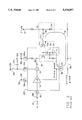
- FIG. 3 depicts an integrated circuit receiver utilizing the conventional method for coupling off-chip and on-chip resonator portions.
- Package 200 encapsulates RF input amplifier 11, mixer 13, local oscillator 16 and an on-chip resonator portion 31.
- Various signals are coupled to/from the encapsulated circuits via a plurality of pins, each represented by a series parasitic inductance: 5 Volt DC power 33a via inductors 32a and 32aa; RF input 10 via inductor 32b; off-chip system ground 33c via inductor 32c; and, IF output 15 via inductor 32d.
- the coupling between on-chip resonator portion 31 and off-chip resonator portion 35 utilizes inductor 32e, which represents the inductance of the package pin.
- the off-chip resonator portion 35 includes an effective inductor 32ee, which represents the net lumped inductance of any off-chip inductive elements such as wires, discrete inductors and the series lead inductance of the varactor 35v.
- the receiver of FIG. 3 also includes a plurality of DC blocking capacitors, 36a-d, each of which serves the conventional DC isolation function.
- the receiver of FIG. 3 employs a varactor 35v as a tuning element, the capacitance of which varies with the DC tuning voltage 34.
- the capacitance of varactor 35v subtracts from and reduces of the effective inductance in the overall resonator circuit, which, in this case, includes inductors 32e, 32ee and 32c.
- the resonator circuit thus comprises the loop 38 formed by capacitors 31a and 31b of on-chip resonator portion 31; inductors 32e and 32ee, blocking capacitor 36d (which has essentially no effect) and varactor 36d of off-chip resonator portion 35; and the series parasitic ground inductance 32c, which closes the loop of the resonator circuit.
- inductor 32c represents the effective series inductance between the off-chip ground node 33c and the on-chip ground node 37. Where, as is frequently done, multiple pins are used to connect the off-chip and on-chip grounds, the effective inductance 32c will be reduced. In the preferred embodiment, in which ten pins connect to the off-chip ground, this effective inductance 32c is approximately 0.1 nH.
- the peak transient current flowing in the resonator loop 38 can reach 100 mA.
- the transient current through inductor 32c induces a computed (i.e. 2 ⁇ f LO L eff l peak ) bounce in the on-chip ground voltage of more than 1 Volt!
- PSRR power supply rejection ratio
- FIG. 4 schematically depicts the coupling of off-chip and on-chip resonator portions in accordance with the invention.
- off-chip resonator portion 35 is connected to on-chip resonator portion via so-called floating resonator coupling pins 43a-b.
- a floating pin is a pin that is not connected, off-chip, directly to a low impedance DC source or ground node. Accordingly, a floating pin connects to an off-chip node at which the impedance conditions are such that the voltage is relatively free to float or vary.
- pin 39 (FIG. 3 and 4) is clearly not floating pins since it connects directly to the off-chip ground node 330.
- resonator coupling pin 43b a floating pin having a parasitic series inductance 42, conducts a large resonator transient current 11 .
- the transient current in inductor 42 induces an LO frequency transient voltage across inductor 42 of approximately 1 Volt.
- inductor 42 i.e., pin 43b
- inductor 42 is directly connected to an off-chip node 46 which is free to float
- it is largely node 46, rather than the on-chip ground node 37, which absorbs the LO frequency voltage swing induced by inductor 42.
- the LO frequency noise in the on-chip ground is greatly reduced, and so is the LO leakage.
- the LO leakage at certain frequencies is reduced as much as 28 dBm--and with no added cost
- resonator coupling pins i.e., those pins used exclusively to couple signals between the off-chip and on-chip portions of the resonator, for example, pin 43a in FIG. 3 and pins 43a-b in FIG. 4.
- the net current leaving the integrated circuit package 200 via the resonator coupling pins will be approximately zero.
- the net current leaving package 200 via the sole resonator coupling pin 43a is not approximately zero. Indeed, it is approximately 100 mA.
- the net current exiting package 200 via the two resonator coupling pins 43a-b is approximately zero since, at all times, these pins conduct approximately equal but opposite currents, l1 and l2a respectively.
- the invention is not limited to circuits using two resonator coupling pins. Nonetheless, embodiments of the invention utilizing more than two resonator coupling pins still exhibit the property that the net current leaving the integrated circuit package via the resonator coupling pins is approximately zero.
- Still another way of viewing the invention depicted in FIG. 4 is to look at the transient current cancellation which takes place at the current summing point 37b.
- Summing point 37b combines the +90° transient current 12 with the -90° transient current l1.
- the effective cancellation of resonator transient currents at point 37b largely eliminates such LO frequency transient signals in other portions of the on-chip ground node 37.
- FIGS. 5A-E depict the board layouts for several receivers, specifically showing the coupling between the off-chip varactor portion 35 and the pins of the receiver chip 200.
- the pinouts for chip package 200 are as follows:
- Chip package 200 is mounted to each of the boards 500a-e in the same position.
- Package 200 is oriented such that the Vdd pins, 251d and 251f, contact metalization 501. In this orientation, the dual lines of pins run vertically, with pin 251f, located in the upper left corner of package 200, contacting off-chip ground through metalization 502.
- Pin 251l also contacts off-chip ground via metalization 502.
- the external oscillator output from pin 251j which can be used to drive an external PLL, bonds to metalization 504.
- a large ground metalization 505 contacts the remaining ground pins, 252a-b, 251a-b and 251g-h.
- RF input from pin 251c bonds to metalization 506.
- off-chip resonator portion 35 connects to a single resonator coupling pin 251i via metalization 507.
- the other terminal from off-chip resonator portion 35 connects to the off-chip system ground 33c.
- FIG. 5A shows the conventional resonator coupling depicted schematically in FIG. 3.
- FIG. 5B shows a modification of 5A in which the grounded end of the off-chip resonator portion 35 is connected to the large ground metalization 505 at a point physically close to the resonator coupling pin connection.
- FIG. 5C shows a similar modification in which the grounded terminal of off-chip resonator portion 35 connects to ground metalization 505 at a different location.
- FIGS. 5D and 5E depict off-chip resonator couplings in accordance with the invention.
- ground metalization 505 has been partitioned into two separate pieces, 505a and 505b.
- Metalization 505a couples off-chip ground to five of the six ground pins previously connected to metalization 505.
- the separated piece, 505b connects to pin 252b, which is now being used as a floating, resonator coupling pin.
- a 75 nH inductor 520 is connected between the two Vdd pins in order to provide additional isolation of high-frequency transient signals.
- FIG. 6 shows comparative plots of the LO leakage as a function of frequency for the board layouts depicted in FIGS. 5A-E.
- Traces 600a-c show the LO leakage for boards 500a-c, respectively.
- the preferred embodiments of the invention, boards 500d and 500e, are shown as traces 600d and 600e, respectively.
- the substantial improvement in LO leakage realized by the invention is clearly evident. This improvement is particularly pronounced at the higher LO frequencies.
Landscapes
- Engineering & Computer Science (AREA)
- Power Engineering (AREA)
- Inductance-Capacitance Distribution Constants And Capacitance-Resistance Oscillators (AREA)
Abstract
Description
______________________________________ Pin # Signal ______________________________________ 251a GND 251b GND251c RF Input 252a GND 251d Vdd 251e IF251h GND 251i LO (i.e., external resonator) Output 251fGND 251g GND252b 251k Vdd 251l GND ______________________________________GND 251j OSC
Claims (9)
Priority Applications (2)
| Application Number | Priority Date | Filing Date | Title |
|---|---|---|---|
| US08/003,897 US5428837A (en) | 1993-01-13 | 1993-01-13 | Method and apparatus for reducing local oscillator leakage in integrated circuit receivers |
| PCT/US1994/000389 WO1994016502A1 (en) | 1993-01-13 | 1994-01-12 | Method and apparatus for reducing local oscillator leakage in integrated circuit receivers |
Applications Claiming Priority (1)
| Application Number | Priority Date | Filing Date | Title |
|---|---|---|---|
| US08/003,897 US5428837A (en) | 1993-01-13 | 1993-01-13 | Method and apparatus for reducing local oscillator leakage in integrated circuit receivers |
Publications (1)
| Publication Number | Publication Date |
|---|---|
| US5428837A true US5428837A (en) | 1995-06-27 |
Family
ID=21708123
Family Applications (1)
| Application Number | Title | Priority Date | Filing Date |
|---|---|---|---|
| US08/003,897 Expired - Lifetime US5428837A (en) | 1993-01-13 | 1993-01-13 | Method and apparatus for reducing local oscillator leakage in integrated circuit receivers |
Country Status (2)
| Country | Link |
|---|---|
| US (1) | US5428837A (en) |
| WO (1) | WO1994016502A1 (en) |
Cited By (19)
| Publication number | Priority date | Publication date | Assignee | Title |
|---|---|---|---|---|
| US5574405A (en) * | 1995-08-22 | 1996-11-12 | Lucent Technologies Inc. | Low noise amplifier/mixer/frequency synthesizer circuit for an RF system |
| US5625307A (en) * | 1992-03-03 | 1997-04-29 | Anadigics, Inc. | Low cost monolithic gallium arsenide upconverter chip |
| US5850595A (en) * | 1993-12-03 | 1998-12-15 | Deutsche Thomson-Brandt Gmbh | Arrangement for reducing interference in tuned circuits in integrated circuits |
| EP0932252A2 (en) * | 1998-01-23 | 1999-07-28 | Matsushita Electric Industrial Co., Ltd. | Tuning demodulator for digitally modulated RF signals |
| US5940750A (en) * | 1994-05-18 | 1999-08-17 | Wang; Guan-Wu | Low-cost low noise block down-converter with a self-oscillating mixer for satellite broadcast receivers |
| US5969667A (en) * | 1997-10-16 | 1999-10-19 | Automotive Systems Laboratory, Inc. | Radar system |
| US5995818A (en) * | 1996-07-30 | 1999-11-30 | Trw Inc. | Low noise block downconverter |
| US6160425A (en) * | 1998-05-08 | 2000-12-12 | Nec Corporation | Frequency converter |
| US6243569B1 (en) | 1998-08-12 | 2001-06-05 | Analog Devices, Inc. | Direct conversion circuit for radio frequency signals |
| US6477148B1 (en) | 1997-02-20 | 2002-11-05 | Telefonaktiebolaget L M Ericsson (Publ) | Radio transceiver on a chip |
| EP1303038A1 (en) * | 2001-10-12 | 2003-04-16 | Kabushiki Kaisha Toshiba | Input circuit for tuner and semiconductor device |
| US20040071252A1 (en) * | 2002-10-10 | 2004-04-15 | International Business Machines Corporation | Charge pump with transient current correction |
| US20040097214A1 (en) * | 2002-11-15 | 2004-05-20 | Kevin Gard | Direct conversion with variable amplitude LO signals |
| US6745019B1 (en) * | 2000-02-15 | 2004-06-01 | Nera A.S.A. | Process and system for reducing leakage of local oscillator |
| US6911739B1 (en) * | 2003-01-29 | 2005-06-28 | Marvell International Ltd. | Methods and apparatus for improving high frequency input/output performance |
| US20050255806A1 (en) * | 2004-05-17 | 2005-11-17 | Korea Electronics Technology Institute | 2N-order sub-harmonic frequency modulator having high carrier suppression ratio and direct conversion transmitter using the same |
| US7002220B1 (en) | 2003-01-29 | 2006-02-21 | Marvell International Ltd. | ESD protection circuit |
| US7123899B1 (en) | 2000-09-06 | 2006-10-17 | Industrial Technology Research Institute | Broadband single-ended input upconverter |
| US7456655B1 (en) | 2005-05-16 | 2008-11-25 | Marvell Israel (Misl) Ltd. | System and process for overcoming wire-bond originated cross-talk |
Citations (18)
| Publication number | Priority date | Publication date | Assignee | Title |
|---|---|---|---|---|
| US3626302A (en) * | 1969-09-23 | 1971-12-07 | Sony Corp | Local oscillator radiation preventing frequency converter circuit |
| US4355420A (en) * | 1979-12-03 | 1982-10-19 | Nippon Electric Co., Ltd. | Frequency converter capable of eliminating local power leak |
| JPS604317A (en) * | 1983-06-23 | 1985-01-10 | Fujitsu Ltd | Frequency converter |
| JPS61105914A (en) * | 1984-10-30 | 1986-05-24 | Nec Corp | Mixer circuit |
| US4662001A (en) * | 1985-08-15 | 1987-04-28 | Zenith Electronics Corporation | Tunable notch filter for image frequency and conducted local oscillator leakage rejection |
| US4759078A (en) * | 1986-11-14 | 1988-07-19 | Rose Communication Systems, Inc. | Coordinated local oscillator receiving system |
| US4791521A (en) * | 1987-04-07 | 1988-12-13 | Western Digital Corporation | Method and apparatus for reducing transient noise by premagnetization of parasitic inductance |
| US4811425A (en) * | 1987-01-09 | 1989-03-07 | Itt Avionics, A Division Of Itt Corporation | Apparatus for reducing the effects of local oscillator leakage in mixers employed in zero IF receivers |
| GB2218591A (en) * | 1988-05-14 | 1989-11-15 | John David Middleton | Apparatus for sensing a person |
| US4890301A (en) * | 1987-11-27 | 1989-12-26 | Telefonaktiebolaget L M Ericsson | Arrangement for compensating errors in a quadrature modulator |
| US4918706A (en) * | 1988-12-28 | 1990-04-17 | Sperry Marine Inc. | Spread spectrum long loop receiver |
| JPH02124608A (en) * | 1988-11-02 | 1990-05-11 | Nec Corp | Frequency conversion circuit |
| JPH02128506A (en) * | 1988-11-08 | 1990-05-16 | Nippon Telegr & Teleph Corp <Ntt> | Oscillation mixing circuit |
| US4952822A (en) * | 1987-11-20 | 1990-08-28 | U.S. Philips Corporation | Integrated logic circuit with instability damping |
| US4982120A (en) * | 1989-07-03 | 1991-01-01 | Dell Corporate Services Corporation | Power supply decoupling mechanism for integrated circuits |
| US5001773A (en) * | 1988-06-20 | 1991-03-19 | Hughes Aircraft Company | Local oscillator feedthru cancellation circuit |
| US5001724A (en) * | 1989-01-13 | 1991-03-19 | Hewlett-Packard Company | Method and apparatus for measuring phase accuracy and amplitude profile of a continuous-phase-modulated signal |
| US5086512A (en) * | 1988-04-20 | 1992-02-04 | Hewlett-Packard Company | Compensation system for dynamically tracking and nulling local oscillator feedthrough |
-
1993
- 1993-01-13 US US08/003,897 patent/US5428837A/en not_active Expired - Lifetime
-
1994
- 1994-01-12 WO PCT/US1994/000389 patent/WO1994016502A1/en active Application Filing
Patent Citations (18)
| Publication number | Priority date | Publication date | Assignee | Title |
|---|---|---|---|---|
| US3626302A (en) * | 1969-09-23 | 1971-12-07 | Sony Corp | Local oscillator radiation preventing frequency converter circuit |
| US4355420A (en) * | 1979-12-03 | 1982-10-19 | Nippon Electric Co., Ltd. | Frequency converter capable of eliminating local power leak |
| JPS604317A (en) * | 1983-06-23 | 1985-01-10 | Fujitsu Ltd | Frequency converter |
| JPS61105914A (en) * | 1984-10-30 | 1986-05-24 | Nec Corp | Mixer circuit |
| US4662001A (en) * | 1985-08-15 | 1987-04-28 | Zenith Electronics Corporation | Tunable notch filter for image frequency and conducted local oscillator leakage rejection |
| US4759078A (en) * | 1986-11-14 | 1988-07-19 | Rose Communication Systems, Inc. | Coordinated local oscillator receiving system |
| US4811425A (en) * | 1987-01-09 | 1989-03-07 | Itt Avionics, A Division Of Itt Corporation | Apparatus for reducing the effects of local oscillator leakage in mixers employed in zero IF receivers |
| US4791521A (en) * | 1987-04-07 | 1988-12-13 | Western Digital Corporation | Method and apparatus for reducing transient noise by premagnetization of parasitic inductance |
| US4952822A (en) * | 1987-11-20 | 1990-08-28 | U.S. Philips Corporation | Integrated logic circuit with instability damping |
| US4890301A (en) * | 1987-11-27 | 1989-12-26 | Telefonaktiebolaget L M Ericsson | Arrangement for compensating errors in a quadrature modulator |
| US5086512A (en) * | 1988-04-20 | 1992-02-04 | Hewlett-Packard Company | Compensation system for dynamically tracking and nulling local oscillator feedthrough |
| GB2218591A (en) * | 1988-05-14 | 1989-11-15 | John David Middleton | Apparatus for sensing a person |
| US5001773A (en) * | 1988-06-20 | 1991-03-19 | Hughes Aircraft Company | Local oscillator feedthru cancellation circuit |
| JPH02124608A (en) * | 1988-11-02 | 1990-05-11 | Nec Corp | Frequency conversion circuit |
| JPH02128506A (en) * | 1988-11-08 | 1990-05-16 | Nippon Telegr & Teleph Corp <Ntt> | Oscillation mixing circuit |
| US4918706A (en) * | 1988-12-28 | 1990-04-17 | Sperry Marine Inc. | Spread spectrum long loop receiver |
| US5001724A (en) * | 1989-01-13 | 1991-03-19 | Hewlett-Packard Company | Method and apparatus for measuring phase accuracy and amplitude profile of a continuous-phase-modulated signal |
| US4982120A (en) * | 1989-07-03 | 1991-01-01 | Dell Corporate Services Corporation | Power supply decoupling mechanism for integrated circuits |
Cited By (48)
| Publication number | Priority date | Publication date | Assignee | Title |
|---|---|---|---|---|
| US5625307A (en) * | 1992-03-03 | 1997-04-29 | Anadigics, Inc. | Low cost monolithic gallium arsenide upconverter chip |
| US5850595A (en) * | 1993-12-03 | 1998-12-15 | Deutsche Thomson-Brandt Gmbh | Arrangement for reducing interference in tuned circuits in integrated circuits |
| US5940750A (en) * | 1994-05-18 | 1999-08-17 | Wang; Guan-Wu | Low-cost low noise block down-converter with a self-oscillating mixer for satellite broadcast receivers |
| US5574405A (en) * | 1995-08-22 | 1996-11-12 | Lucent Technologies Inc. | Low noise amplifier/mixer/frequency synthesizer circuit for an RF system |
| US5995818A (en) * | 1996-07-30 | 1999-11-30 | Trw Inc. | Low noise block downconverter |
| US7580683B2 (en) | 1997-02-20 | 2009-08-25 | Telefonaktiebolaget Lm Ericsson (Publ) | Radio transceiver on a chip |
| US20090268643A1 (en) * | 1997-02-20 | 2009-10-29 | Telefonaktiebolaget L M Ericssson (Publ) | Radio transceiver on a chip |
| US20060062165A1 (en) * | 1997-02-20 | 2006-03-23 | Gardenfors Karl Hakan T | Radio transceiver on a chip |
| US7149191B2 (en) | 1997-02-20 | 2006-12-12 | Telefonaktiebolaget Lm Ericsson (Publ) | Radio transceiver on a chip |
| US7269144B2 (en) | 1997-02-20 | 2007-09-11 | Telefonaktiebolaget Lm Ericsson (Publ) | Radio transceiver on a chip |
| US6477148B1 (en) | 1997-02-20 | 2002-11-05 | Telefonaktiebolaget L M Ericsson (Publ) | Radio transceiver on a chip |
| US8005439B2 (en) | 1997-02-20 | 2011-08-23 | Telefonaktiebolaget L M Ericsson (Publ) | Radio transceiver on a chip |
| US20040198299A1 (en) * | 1997-02-20 | 2004-10-07 | Gardenfors Karl Hakan Torbjorn | Radio transceiver on a chip |
| US6633550B1 (en) | 1997-02-20 | 2003-10-14 | Telefonaktiebolaget Lm Ericsson (Publ) | Radio transceiver on a chip |
| US7068171B2 (en) | 1997-02-20 | 2006-06-27 | Telefonaktiebolaget Lm Ericsson (Publ) | Radio transceiver on a chip |
| US20050130700A1 (en) * | 1997-02-20 | 2005-06-16 | Karl Hakan Torbjorn Gardenfors | Radio transceiver on a chip |
| MY119790A (en) * | 1997-02-20 | 2005-07-29 | Ericsson Telefon Ab L M | Radio transceiver on a chip |
| US8626086B2 (en) | 1997-02-20 | 2014-01-07 | Telefonaktiebolaget L M Ericssson (Publ) | Radio transceiver on a chip |
| US8954020B2 (en) | 1997-02-20 | 2015-02-10 | Telefonaktiebolaget L M Ericsson (Publ) | Radio transceiver on a chip |
| US20040192223A1 (en) * | 1997-02-20 | 2004-09-30 | Telefonaktiebolager L M Ericsson | Radio transceiver on a chip |
| US5969667A (en) * | 1997-10-16 | 1999-10-19 | Automotive Systems Laboratory, Inc. | Radar system |
| EP0932252A3 (en) * | 1998-01-23 | 1999-12-08 | Matsushita Electric Industrial Co., Ltd. | Tuning demodulator for digitally modulated RF signals |
| US6668025B1 (en) | 1998-01-23 | 2003-12-23 | Matsushita Electric Industrial Co., Ltd. | Tuning demodulator for digitally modulated RF signals |
| EP0932252A2 (en) * | 1998-01-23 | 1999-07-28 | Matsushita Electric Industrial Co., Ltd. | Tuning demodulator for digitally modulated RF signals |
| US6160425A (en) * | 1998-05-08 | 2000-12-12 | Nec Corporation | Frequency converter |
| US6731923B2 (en) | 1998-08-12 | 2004-05-04 | Analog Devices, Inc. | Direct conversion circuit for radio frequency signals |
| US6243569B1 (en) | 1998-08-12 | 2001-06-05 | Analog Devices, Inc. | Direct conversion circuit for radio frequency signals |
| US6745019B1 (en) * | 2000-02-15 | 2004-06-01 | Nera A.S.A. | Process and system for reducing leakage of local oscillator |
| US7123899B1 (en) | 2000-09-06 | 2006-10-17 | Industrial Technology Research Institute | Broadband single-ended input upconverter |
| EP1303038A1 (en) * | 2001-10-12 | 2003-04-16 | Kabushiki Kaisha Toshiba | Input circuit for tuner and semiconductor device |
| US20030073421A1 (en) * | 2001-10-12 | 2003-04-17 | Kabushiki Kaisha Toshiba | Input circuit for tuner and semiconductor device |
| US7162001B2 (en) * | 2002-10-10 | 2007-01-09 | International Business Machines Corporation | Charge pump with transient current correction |
| US20040071252A1 (en) * | 2002-10-10 | 2004-04-15 | International Business Machines Corporation | Charge pump with transient current correction |
| US7460849B2 (en) | 2002-11-15 | 2008-12-02 | Qualcomm Incorporated | Direct conversion with variable amplitude LO signals |
| US8526904B2 (en) | 2002-11-15 | 2013-09-03 | Qualcomm Incorporated | Direct conversion with variable amplitude LO signals |
| US7027793B2 (en) | 2002-11-15 | 2006-04-11 | Qualcomm Incorporated | Direct conversion with variable amplitude LO signals |
| US20090111419A1 (en) * | 2002-11-15 | 2009-04-30 | Qualcomm Incorporated | Direct conversion with variable amplitude lo signals |
| US20040097214A1 (en) * | 2002-11-15 | 2004-05-20 | Kevin Gard | Direct conversion with variable amplitude LO signals |
| US6987326B1 (en) | 2003-01-29 | 2006-01-17 | Marvell International Ltd. | Methods and apparatus for improving high frequency input/output performance |
| US7751164B1 (en) | 2003-01-29 | 2010-07-06 | Marvell International Ltd. | Electrostatic discharge protection circuit |
| US6977444B1 (en) | 2003-01-29 | 2005-12-20 | Marvell International Ltd. | Methods and apparatus for improving high frequency input/output performance |
| US7002220B1 (en) | 2003-01-29 | 2006-02-21 | Marvell International Ltd. | ESD protection circuit |
| US6911739B1 (en) * | 2003-01-29 | 2005-06-28 | Marvell International Ltd. | Methods and apparatus for improving high frequency input/output performance |
| US7009308B1 (en) | 2003-01-29 | 2006-03-07 | Xiaodong Jin | Methods and apparatus for improving high frequency input/output performance |
| US20050255806A1 (en) * | 2004-05-17 | 2005-11-17 | Korea Electronics Technology Institute | 2N-order sub-harmonic frequency modulator having high carrier suppression ratio and direct conversion transmitter using the same |
| US7324798B2 (en) * | 2004-05-17 | 2008-01-29 | Korea Electronics Technology Institute | 2N-order sub-harmonic frequency modulator having high carrier suppression ratio and direct conversion transmitter using the same |
| US7456655B1 (en) | 2005-05-16 | 2008-11-25 | Marvell Israel (Misl) Ltd. | System and process for overcoming wire-bond originated cross-talk |
| US8922246B1 (en) | 2005-05-16 | 2014-12-30 | Marvell Israel (M.I.S.L) Ltd. | System and process for overcoming wire-bond originated cross-talk |
Also Published As
| Publication number | Publication date |
|---|---|
| WO1994016502A1 (en) | 1994-07-21 |
Similar Documents
| Publication | Publication Date | Title |
|---|---|---|
| US5428837A (en) | Method and apparatus for reducing local oscillator leakage in integrated circuit receivers | |
| US6873299B2 (en) | Dual resonance antenna apparatus | |
| US5789995A (en) | Low loss electronic radio frequency switch | |
| US5231361A (en) | Voltage controlled push-push oscillator with parallel resonant tank circuits | |
| KR100639589B1 (en) | Antenna switch | |
| US7209011B2 (en) | Method and apparatus for synthesizing high-frequency signals for wireless communications | |
| USRE40620E1 (en) | Fully integrated All-CMOS AM transmitter with automatic antenna tuning | |
| US20070085617A1 (en) | Amplifier arrangement for ultra-wideband applications and method | |
| USRE41207E1 (en) | Fully integrated ALL- CMOS AM transmitter with automatic antenna tuning | |
| US6529720B1 (en) | Integrated circuit of inductive elements | |
| JP2002176375A (en) | Semiconductor integrated switch circuit | |
| GB2225683A (en) | High frequency amplifier prevents parametric oscillations | |
| KR100303176B1 (en) | Balanced integrated circuit elements operating as parallel resonant circuits | |
| US5418500A (en) | High-frequency oscillator circuit | |
| US3699452A (en) | Active antenna arrangement for a plurality of frequency ranges | |
| KR100260965B1 (en) | Amplifier and portable telephone apparatus using the same | |
| US7362193B2 (en) | Oscillator and an integrated circuit | |
| EP0941574B1 (en) | Oscillator | |
| US7046982B2 (en) | High frequency device having a frame with segmented compartments for prevented unwanted signal propagation | |
| EP1931028B1 (en) | Variable tuning circuit using variable capacitance diode and television tuner | |
| KR100819134B1 (en) | Integrated Circuit Package Having An Inductance Loop Formed From A Multi-loop Configuration | |
| RU2147391C1 (en) | Local oscillator noise suppression circuit | |
| KR100285307B1 (en) | Voltage controlled oscillator device using coaxial resonator | |
| US6369664B1 (en) | Voltage controlled oscillator and electronic apparatus using same | |
| US20030098750A1 (en) | Oscillator module and electronic apparatus using the same |
Legal Events
| Date | Code | Title | Description |
|---|---|---|---|
| AS | Assignment |
Owner name: ANADIGICS, INC., NEW JERSEY Free format text: ASSIGNMENT OF ASSIGNORS INTEREST;ASSIGNORS:BAYRUNS, ROBERT J.;SWEENEY, SCOTT D.;LOPEZ, OSVALDO J.;REEL/FRAME:006838/0279 Effective date: 19940120 |
|
| STCF | Information on status: patent grant |
Free format text: PATENTED CASE |
|
| FPAY | Fee payment |
Year of fee payment: 4 |
|
| FEPP | Fee payment procedure |
Free format text: PAT HOLDER CLAIMS SMALL ENTITY STATUS, ENTITY STATUS SET TO SMALL (ORIGINAL EVENT CODE: LTOS); ENTITY STATUS OF PATENT OWNER: SMALL ENTITY |
|
| FEPP | Fee payment procedure |
Free format text: PAT HOLDER NO LONGER CLAIMS SMALL ENTITY STATUS, ENTITY STATUS SET TO UNDISCOUNTED (ORIGINAL EVENT CODE: STOL); ENTITY STATUS OF PATENT OWNER: SMALL ENTITY |
|
| REFU | Refund |
Free format text: REFUND - PAYMENT OF MAINTENANCE FEE, 8TH YR, SMALL ENTITY (ORIGINAL EVENT CODE: R2552); ENTITY STATUS OF PATENT OWNER: SMALL ENTITY |
|
| FPAY | Fee payment |
Year of fee payment: 8 |
|
| FEPP | Fee payment procedure |
Free format text: ENTITY STATUS SET TO UNDISCOUNTED (ORIGINAL EVENT CODE: BIG.); ENTITY STATUS OF PATENT OWNER: SMALL ENTITY |
|
| FEPP | Fee payment procedure |
Free format text: PAT HOLDER CLAIMS SMALL ENTITY STATUS, ENTITY STATUS SET TO SMALL (ORIGINAL EVENT CODE: LTOS); ENTITY STATUS OF PATENT OWNER: SMALL ENTITY |
|
| FPAY | Fee payment |
Year of fee payment: 12 |
|
| AS | Assignment |
Owner name: II-VI OPTOELECTRONIC DEVICES, INC., NEW JERSEY Free format text: CHANGE OF NAME;ASSIGNOR:ANADIGICS, INC.;REEL/FRAME:042381/0761 Effective date: 20160729 |
|
| AS | Assignment |
Owner name: SKYWORKS SOLUTIONS, INC., MASSACHUSETTS Free format text: ASSIGNMENT OF ASSIGNORS INTEREST;ASSIGNOR:II-VI OPTOELECTRONIC DEVICES, INC.;REEL/FRAME:042551/0708 Effective date: 20170308 |