US5446898A - Method and apparatus for configuring and installing a loadable ABIOS device support layer in a computer system - Google Patents
Method and apparatus for configuring and installing a loadable ABIOS device support layer in a computer system Download PDFInfo
- Publication number
- US5446898A US5446898A US07/902,134 US90213492A US5446898A US 5446898 A US5446898 A US 5446898A US 90213492 A US90213492 A US 90213492A US 5446898 A US5446898 A US 5446898A
- Authority
- US
- United States
- Prior art keywords
- volatile memory
- microcode
- microprocessor
- operating system
- memory
- Prior art date
- Legal status (The legal status is an assumption and is not a legal conclusion. Google has not performed a legal analysis and makes no representation as to the accuracy of the status listed.)
- Expired - Lifetime
Links
Images


Classifications
-
- G—PHYSICS
- G06—COMPUTING; CALCULATING OR COUNTING
- G06F—ELECTRIC DIGITAL DATA PROCESSING
- G06F9/00—Arrangements for program control, e.g. control units
- G06F9/06—Arrangements for program control, e.g. control units using stored programs, i.e. using an internal store of processing equipment to receive or retain programs
- G06F9/44—Arrangements for executing specific programs
- G06F9/4401—Bootstrapping
- G06F9/4403—Processor initialisation
Definitions
- This invention relates to personal computer systems and, more particularly, to a method and apparatus for configuring and installing firmware.
- a personal computer system can usually be defined as a desk top, floor standing, or portable computer that includes a system unit having a system processor, a display monitor, a keyboard, one or more diskette drives, a fixed disk storage, an optional pointing device such as a "mouse,” and an optional printer.
- system processor a system processor
- display monitor a keyboard
- diskette drives a system that stores data
- fixed disk storage a fixed disk storage
- an optional pointing device such as a "mouse”
- printer optional printer
- the first family usually referred to as Family 1 Models, uses a bus architecture exemplified by the AT computer and other "IBM compatible" machines.
- the second family referred to as Family 2 Models, uses IBM's MICRO CHANNEL bus architecture exemplified by IBM's PS/2 Models 50 through 95.
- the bus architectures used in Family 1 and Family 2 models are well known in the art.
- the system processor of the personal computer is from the Intel 86 Family of microprocessors.
- the Intel 86 Family of processors includes the 8088, 8086, 80286, 80386, and 80486 processors commercially available from Intel Corporation.
- the architecture of the Intel 86 Family of processors provides an upwardly compatible instruction set which assists in preserving software investments from previous processors in the 86 Family of processors. This upward compatibility preserves the software application base of the personal computers which use this family of processors.
- the PC and XT computers use the Intel 8088 processor.
- the AT computers use the Intel 80286 processor.
- the PS/2 line spans several of the Intel processors. More specifically, a PS/2 Model 30, which is similar to the IBM PC and XT, uses an Intel 8086 processor.
- the PS/2 Models 50 and 60 both use the Intel 80286 processors.
- the Intel 80386 processor is used in the IBM PS/2 Model 80 and certain versions of the IBM PS/2 Model 70. Other versions of the IBM PS/2 Model 70, as well as the PS/2 Models 90 XP 486 and 95 XP 486, use the Intel 80486 processor.
- the processors in the Intel 86 Family support a variety of operating modes.
- Real mode which supports a one megabyte system address space, is the only operating mode of the 8088 and 8086 processors.
- the 80286 supports both a real and a protected operating mode.
- Protected mode provides a mode of operation which prevents an application from interfering with the operation of other applications or the operating system.
- the 80286 provides extended addressing capabilities, allowing up to sixteen megabytes of memory to be addressed directly. To maintain downward compatibility, the 80286 can be operated in real mode to emulate the real mode of the 8088 or 8086.
- the 80386 and 80486 can address up to four gigabytes of physical memory.
- the 80386 and 80486 also support a virtual 86 mode of operation.
- the virtual 86 mode supports the operational characteristics of the real mode within the overall confines of the protected mode environment.
- BIOS basic input/output system
- BIOS was an integral part of the computer system and controlled the movement of data in and out of the system processor, it was resident on a system planar board of the system unit and was shipped to the user in either a read-only memory (ROM) or an erasable programmable read-only memory (EPROM).
- BIOS in the original IBM PC occupied 8 K bytes (a kilobyte or "K byte” refers to a quantity of 1024 bytes) of ROM resident on the planar board.
- the ROM also contained a power-on self test (POST) program which was used to test and initialize the computer system.
- POST power-on self test
- the accumulation of code resident in the computer "system ROM became known as the "system firmware,” or simply firmware.”
- the firmware included a POST portion and a BIOS portion.
- BIOS was defined to include the POST program.
- BIOS Advanced BIOS
- CBIOS Compatibility BIOS
- Personal computer systems may be linked to form a network of computers (e.g., a Local Area Network (LAN)) so that users can exchange information, share I/O devices, and utilize a particular direct access storage device (DASD) such as a particular hardfile or diskette.
- a network of computers e.g., a Local Area Network (LAN)
- DASD direct access storage device
- the LAN includes a client and a server.
- a server is a computer system which includes a DASD for supplying the storage for one or more clients of the local area network.
- a client or server may require modifications, updates, extensions or maintenances of the system firmware.
- An object of the present invention is to provide a configuration procedure in which a requirement for ABIOS can be determined and stored within the system.
- Another object of the present invention is to provide a program installation procedure capable of supporting a loadable ABIOS.
- FIG. 1A is a perspective view of a typical personal computer system
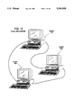
- FIG. 1B is a diagram of a typical local area network
- FIG. 2 is a block schematic diagram of a unified planar board for the computer system of FIG. 1A;
- FIG. 3 is a block schematic diagram of an alternative planar board for the computer system of FIG. 1A;
- FIG. 4 is a block schematic diagram of a processor card for use with the alternative planar board of FIG. 3;
- FIG. 5A is a diagram of the system address space for the computer system of FIG. 1A;
- FIG. 5B is a diagram of a typical firmware memory map
- FIG. 6 is a flow diagram of a system initialization sequence as it pertains to ABIOS
- FIG. 7 is a diagram of an enhanced delivery mechanism for ABIOS
- FIG. 8 is a flow diagram of the internals of ABIOS initialization
- FIG. 9 is an ABIOS program module header
- FIG. 10A is a diagram of NVRAM showing the data area used in the present invention.
- FIG. 10B is a flow diagram of a configuration method as it relates to the present invention.
- FIG. 11 is a flow diagram of an operating system install operation as it relates to ABIOS.
- the personal computer system 100 includes a system unit 102 having a suitable enclosure or casing 103, output device or monitor 104 (such as a conventional video display), input devices such as a keyboard 110, an optional mouse 112, and an optional output device such as a printer 114.
- the system unit 102 may include one or more mass storage devices such as a diskette drive 108 (operable with a diskette-not shown) and a hard disk drive (hardfile) 106.
- system unit 102 may be connected electronically in a well-known manner with other system units 102B to form a local area network (LAN).
- system unit 102 functions as the server and system units 102B function as the clients.
- System units 102B are identical to the unit 102, except that units 102B include no drives 106, 108 and are thus referred to as medialess clients.
- Other conventional I/O devices may be connected to the system units 102, 102B for interaction therewith.
- the planar 200 includes a printed circuit board (PCB) 201 upon which are mounted or connected a number of input/output bus connectors 232 having I/O slots, a processor 202 which is connected by a high speed CPU local bus 210 under control of a bus control unit 214 to a memory control unit 256.
- the unit 256 is further connected to a main memory such as volatile random access memory (RAM) 264.
- RAM volatile random access memory
- Any appropriate processor 202 can be used such as an Intel 80386, Intel 80486 or the like.
- a system power connector 205 is mounted on the PCB 201 for connection to a power unit (not shown) that supplies the necessary power for the system 100.
- the CPU local bus 210 (comprising address, data and control components) provides for the interconnection of the processor 202, an optional math coprocessor 204, an optional cache controller 206, and an optional cache memory 208. Also coupled onto the CPU local bus 210 is a system buffer 212.
- the system buffer 212 is itself connected to a system bus 216 which comprises address, data and control components.
- the system bus 216 extends between the system buffer 212 and an I/O buffer 228.
- the system bus 216 is further connected to the bus control unit 214 and to a direct memory access (DMA) control unit 220.
- the DMA control unit 220 includes a central arbiter 224 and a DMA controller 222.
- the I/O buffer 228 provides an interface between the system bus 216 and an I/O bus 230.
- An oscillator 207 is connected as shown for providing suitable clock signals to the computer system 100.
- Those skilled in the art will recognize that while the preferred embodiment is implemented on the MICRO CHANNEL bus of an IBM PS/2 computer system, which is well known in the art, alternative bus architectures could also be used to employ the invention.
- I/O bus 230 Connected to the I/O bus 230 is a plurality of I/O bus connectors having slots 232 for receiving adapter cards (not shown) which may be further connected to I/O devices or memory (e.g., hardfile 106).
- I/O connectors 232 are shown for convenience, but additional I/O connectors may easily be added to suit the needs of a particular system.
- An arbitration bus 226 couples the DMA controller 222 and the central arbiter 224 to the I/O connectors 232 and a diskette adapter 246.
- the memory control unit 256 Also connected to the system bus 216 is the memory control unit 256 which includes a memory controller 258, an address multiplexer 260, and a data buffer 262.
- the memory control unit 256 is further connected to the main memory such as the random access memory as represented by the RAM module 264.
- the memory control unit 256 includes logic for mapping addresses to and from the processor 202 to and from particular areas of the RAM 264. While the system 100 is shown with a basic one megabyte RAM module 264, it is understood that additional memory can be interconnected as represented in FIG. 2 by optional memory modules 266, 268, 270.
- a buffer 218 is coupled between the system bus 216 and a planar I/O bus 234.
- the planar I/O bus 234 includes address, data, and control components. Coupled along the planar I/O bus 234 are a variety of I/O adapters and other peripheral components such as a display adapter 236 (which is used to drive the optional display 104), a clock/CMOS RAM 250, a nonvolatile RAM 248 (hereinafter referred to as NVRAM), a serial adapter 240 (other common terms used for "serial” are "asynchronous" and "RS232”), a parallel adapter 238, a plurality of timers 252, the diskette adapter 246, a keyboard/mouse controller 244, an interrupt controller 254, and a firmware subsystem 242.
- the firmware subsystem typically includes a nonvolatile program store (e.g., ROM) which contains the POST and BIOS programs.
- the clock/CMOS RAM 250 is used for time of day calculations.
- the NVRAM 248 is used to store system configuration data. That is, the NVRAM 248 will contain values which describe the present configuration of the system 100.
- the NVRAM 248 contains information which describes, for example, adapter card initialization data, capacity of a fixed disk or a diskette, the amount of main memory, etc. Furthermore, these data are stored in NVRAM 248 whenever a configuration program is executed.
- This configuration program can be a conventional Set Configuration program provided on a system Reference Diskette included with IBM PS/2 computer systems. The Reference Diskette is sometimes referred to as a diagnostic, maintenance or service diskette.
- the purpose of the configuration program is to store values characterizing the configuration of this system 100 to NVRAM 248 which are saved when power is removed from the system.
- the NVRAM can be a low power CMOS memory with a battery backup.
- a port A 278 and a port B 280 Connected to the keyboard/mouse controller 244 are a port A 278 and a port B 280. These ports A,B are used to connect the keyboard 110 and the mouse 112 to the personal computer system 100. Coupled to the serial adapter 240 is a serial connector 276. An optional device such as a modem (not shown) can be coupled to the system through this connector 276. Coupled to the parallel adapter 238 is a parallel connector 274 to which a device such as the printer 114 can be connected. Connected to the diskette adapter 246 is a diskette connector 282 used to attach one or more diskette drives 108.
- system unit 102 may also use a planar board 300 and a processor card 400 (FIGS. 3 and 4).
- the processor card 400 is removably mounted on and is electrically connected to the planar board 300.
- Identical element numbers of FIG. 2 correspond to identical elements in FIGS. 3 and 4.
- the planar board 300 comprises a printed circuit board (PCB) 301 upon which are mounted (e.g., surface mounted) various components that are interconnected by wiring or circuits in the PCB.
- PCB printed circuit board
- Such components include a suitable commercially available electrical connector 302 into which an edge 416 of the processor card 400 is plugged for removably mounting and electrically connecting the processor card 400 to the planar board 300.
- a plurality of single in-line memory module (SIMM) connectors 306 is also mounted on the PCB 301 for connecting to memory banks 308A, 308B forming the system main memory or RAM.
- SIMM single in-line memory module
- I/O bus or expansion connectors 232 are also mounted on the PCB 301 for connection to different expansion adapters and options that may be added or incorporated into the personal computer system 100.
- the fixed disk drive 106 may be connected to an adapter card (not shown) having a disk controller which is connected to a connector 232.
- each connector 232 is a commercially available connector of the type conforming to the above-mentioned MICRO CHANNEL architecture.
- a system power connector 205 is mounted on the PCB 301 for connection to a power unit (not shown) that supplies the necessary power for the system.
- a nonvolatile memory (NVRAM) 248 and a time-of-day clock/CMOS RAM 250 are also mounted on the PCB 301.
- the PCB 301 also has mounted thereon various oscillators (not shown) to provide timing signals, and buffers 342, 344 (not all shown) to isolate sections of the circuitry in a manner well known.
- PCB 301 interconnects the various components as shown in the drawing and is grouped into three groupings, a memory bus 310 (including lines 324-338), a channel bus 312 (including an address bus 322, a data bus 320 and a control bus 318), and miscellaneous signal lines including interrupt lines 314, 316, all of which are connected to counterpart wiring on the PCB 401 through the connectors 302, 416.
- Tapped off the bus 312 is a planar function bus 319.
- the processor card 400 for removably mounting on the planar board 300.
- the processor card 400 comprises a printed circuit board (PCB) 401 having mounted (e.g., surface mounted) thereon a plurality of commercially available components including a processor 202, an optional math coprocessor 204, an optional cache controller 206, an optional cache memory 208, a direct memory access (DMA) control unit 220, a bus control unit 214, a memory control unit 256, a firmware subsystem 242, and parity checking units 402, 404.
- the processor 202 preferably is a high performance type, such as an Intel 80486, having thirty-two bit data paths and providing thirty-two bit addressing capability.
- a plurality of buffers 406, 408, 410, 412, 414 is connected as shown.
- the buffers provide selective isolation or connection between the circuits allowing different portions to be used concurrently, for example, to move data between the processor 202 and the cache memory 208 while other data is being transferred between an I/O unit and the main memory 308A, 308B.
- All of the above components are electrically connected to each other as appropriate by printed wiring circuits in PCB 401 which terminate at the edge connector 416.
- the edge connector 416 is pluggable into the edge connector 302 on the planar board 300 shown in FIG. 3 so that the planar board 300 and the processor card 400 are electrically and mechanically interconnectable.
- the wiring circuits of the PCB 401 include a local bus 418 including data, address and control lines 420, 422, 424, respectively, which interconnect the processor 202 with an optional math coprocessor 204, an optional cache controller 206 and an optional cache memory 208, as shown in FIG. 4.
- the remaining circuit lines generally include interrupt lines 316, channel bus lines 312 and memory bus lines 310.
- the channel bus lines 312 include control, data and address bus lines 318, 320, 322, respectively.
- Memory bus lines 310 include multiplexed memory address lines 324, 332, row address strobe (RAS) lines 328, 336 for memory banks 308A, 308B, column address strobe (CAS) line 338, data bus A and B lines 326 and 334, and a line 330 for use in error checking via parity check or ECC checking.
- An oscillator 207 is connected as shown for providing suitable clock signals to the computer system 100. For simplicity, certain miscellaneous lines, such as reset, grounds, power-on, etc. have been omitted from FIGS. 2, 3 and 4.
- the card 400 is electrically and mechanically connected to the board 300 and typically lies in a plane perpendicular to the board 400.
- BIOS Basic Input Output System program
- BIOS further includes the compatibility BIOS or CBIOS and the advanced BIOS or ABIOS.
- POST is the set of instructions which execute when the system is first powered-on to initialize the personal computer system 100.
- BIOS is the set of instructions which facilitates the transfer of data and control instructions between the processor 202 and I/O devices.
- a medialess system unit e.g., 102B
- a suitable network adapter or card for providing a Remote Initial Program Load (RIPL) facility within the unit 102B.
- the card is connected, for example, to one of the connectors 232.
- the RIPL program permits booting an operating system from a network server 102 rather than from a local storage device such as the fixed disk 106 or the diskette 108.
- RIPL is also referred to as simply Remote Program Load or RPL, and the terms are used interchangeably.
- RPL is well understood in the art.
- POST contains a bootstrap program which attempts to locate a boot device and load a boot record.
- the boot device is hardfile 106 or diskette drive 108.
- Diskette drive 108 requires a boot or operating system diskette to operate. If POST successfully loads a boot record from a boot device, then POST transfers control to the boot record, completing the operation of the POST bootstrap program. If a boot record was unable to be loaded and a RPL adapter is present, then POST transfers control to an RPL program. If no RPL program is present, then POST prompts the user indicating that a boot source is required.
- CBIOS is essential to the bootstrap operation of the computer. CBIOS provides a number of services including access to the hardfile 106 and diskette drive 108. ABIOS is demand initialized and normally not a required part of the POST bootstrap process.
- the system address space 500 includes a plurality of memory address regions 502, 504, 506, 508, 510 which are addressable by the processor 202.
- the low memory region 502 is the traditional compatibility space in which real mode programs operate. For example, both DOS and CBIOS are real mode programs.
- the video region 504 occupies a 128K byte address space beginning at a physical location A0000 hex up through a physical location BFFFF hex or the A000 hex and B000 hex segments.
- the video region 504 provides video regeneration buffers; data which are stored in these buffers define what a user sees on the computer display 104.
- the feature region 506 occupies a 128K byte address space beginning at a physical location C0000 hex up through a physical location DFFFF hex or the C000 hex and D000 hex segments.
- the feature region 506 is used to store adapter firmware; this region may also provide buffer space.
- a small computer system interface (SCSI) disk controller adapter includes an adapter firmware ROM containing POST, CBIOS and ABIOS programs which during operation is stored in feature region 506.
- the system firmware region 508 occupies a 128K byte address space beginning at a physical location E0000 hex up through a physical location FFFFF hex or the E000 hex and F000 hex segments.
- the system firmware region 508 stores the system firmware including POST and BIOS.
- the region above a one megabyte boundary is a high or extended memory region 510. High memory 510 is utilized by operating systems such as the OS/2 operating system.
- Extended memory refers to memory above the one megabyte address location. Expanded memory refers to memory which is bank switched into an area below the one megabyte address location. Expanded memory bank switching provides real mode applications with the ability to address more physical memory than the real mode address space directly allows. Expanded memory operation requires an available address space or window to be present in the real mode address space. Expanded memory operation also requires an expanded memory program to manage the bank switching. A common location for the expanded memory window is in the feature space 506 as well as the system firmware space 508. Maximizing the amount of available space for expanded memory windows is a competitive requirement for personal computer systems.
- a firmware image includes an ABIOS portion 554, a CBIOS portion 552, and a POST portion 550.
- an adapter card firmware such as the IBM SCSI adapter card
- the size of the ABIOS portion is approximately 11K bytes.
- the system firmware such as the IBM PS/2 Model 95 XP 486, the size of the ABIOS portion is approximately 32K bytes.
- ABIOS uses substantial portion of the overall address space.
- an ABIOS size of approximately 32K bytes occupies 25% of the system firmware space 508.
- an ABIOS size of 11K bytes uses approximately 70% of the 16K byte range. Additionally, some adapters exceed the 16K byte range.
- FIG. 6 a flow diagram of an operating system bootstrap and initialization process is shown.
- the operating system begins to bootstrap, step 600.
- the operating system then begins some of its preliminary initialization, step 602.
- the type and scope of operating system preliminary initialization is well known.
- the operating system then loads the ABIOS patch modules or files, step 604.
- These patch files normally resident on the operating system boot device, provide functional corrections and enhancements to existing resident ABIOS program code.
- the ABIOS program modules can be listed in a control file such as an ABIOS.SYS.
- This ABIOS.SYS list can be a text file containing the names of the ABIOS modules such as MODULE 1.BIO, MODULE2.BIO, etc.
- step 604 the operating system can then initialize ABIOS, step 606.
- ABIOS is initialized by issuing CBIOS function calls. Once ABIOS is initialized, step 606, the operating system can continue further initialization, step 608.
- CBIOS provides two function calls to support the initialization of ABIOS. These calls are accessed through a CBIOS system services interface defined as software interrupt 15 hex (INT 15H).
- ABIOS initialization is more clearly defined in the IBM Personal System/2 and Personal Computer BIOS Interface Technical Reference Manual.
- the ABIOS 554 is physically separated from the remaining firmware, and packaged as a file on diskette 700 or other media.
- the space occupied by ABIOS in firmware address space 506, 508 is freed.
- Moving ABIOS 554 applies to both the system firmware ABIOS as well as feature space ABIOS. Accordingly, the space normally Occupied by ABIOS in system firmware space 506 is freed and the space normally occupied by ABIOS in feature space 508 is freed.
- ABIOS initialization a flow diagram of ABIOS initialization is shown.
- Step 802 is the redirection of control.
- the CBIOS system services call must redirect control to the ABIOS initialization program now present in the RAM extension area.
- step 800 the CBIOS system services code resident in the system firmware first must locate and transfer control to the now RAM resident ABIOS initialization program. This is done through the previously described "DS" register which specifies the segment address as to where the RAM ABIOS area begins.
- the CBIOS system services program present in the system firmware, obtains the system services call from step 800 and must redirect this call to the ABIOS initialization code now in RAM. This redirection is performed through an indirect call through an entry in the ABIOS header which begins at offset zero of the segment specified by the "DS" register. This ABIOS header is described in more detail in conjunction with FIG. 9.
- a far call is performed to the address specified by DS:[ABIOSINIT], step 802, thus transferring the ABIOS initialization operation to the ABIOS program now in system RAM.
- ABIOSINIT is discussed in greater detail in conjunction with FIG. 9.
- a far jump can be used in place of the far call and the selection of call or jump is a matter of well known design choice.
- ABIOS initialization then performs a set of near call operations designed to initialize ABIOS, step 804.
- ABIOS initialization then performs a ROM scan operation designed to locate and initialize ABIOS present in the adapter firmware address space, step 806.
- a ROM scan is performed by searching for a specific header pattern in the feature space or adapter firmware space (see FIG. 5A).
- ABIOS initialization then performs a RAM scan designed to locate and initialize ABIOS present as a RAM loaded extension or patch, step 808.
- the current ABIOS module the one containing the ABIOS initialization program, need not be searched for in RAM scan thus RAM scan begins after the current module.
- step 808 the system services call to initialize ABIOS is complete, step 810 and control returns to the caller.
- ABIOS module header is shown.
- the field at offset +14H (an offset of 14 hex bytes or 20 decimal bytes), which prior to the present invention was a reserved field, stores an offset of the ABIOS initialization programs.
- the table entry at +14H can be termed ABIOSINIT.
- Other table entries are set forth in the ABIOS section of the IBM Personal System/2 and Personal Computer BIOS Interface Technical Reference Manual.
- NVRAM 248 which includes a location for storing a loadable ABIOS request byte (LARB) 1000 of the present invention is shown.
- NVRAM 248 is read from and written to through standard I/O commands in a conventional manner.
- the LARB 1000 indicates whether the loadable ABIOS is required by the system.
- the LARB 1000 initialization is described below with reference to FIG. 10B.
- a program (e.g., an operating system) installation which uses the LARB 1000 is described below with reference to FIG. 11.
- ADP adapter description program
- the ADP works in conjunction with the Set Configuration program to initialize the NVRAM 248 to indicate that the loadable ABIOS is required by the system. While the Set Configuration program is executing, Set Configuration may execute one or more ADPs.
- An Adapter Description File (ADF) contains a keyword, e.g. Exec, which is used to invoke the execution of an ADP.
- a thorough description of the Set Configuration program, the ADFs and the ADPs is set forth in the Setup section of the IBM Personal System/2 Hardware Interface Technical Reference--Architectures, October 1990.
- Adapter description files are required, for example, for every adapter installed in the system unit such as those that are installed in I/O slots 232. There can also be an ADF for the system 100.
- the flow diagram of FIG. 10B is incorporated into only those ADPs which support a subsystem (e.g., an adapter or a system) which requires a loadable ABIOS.
- the Set Configuration program initiates the execution of an ADP, step 1002.
- the ADP checks the LARB value against a predetermined signature value, such as hex A1, step 1004.
- the LARB is obtained by reading the LARB value from NVRAM 248.
- the LARB can be read directly from NVRAM or through a CBIOS interface. If the LARB does not equal the signature value then the ADP sets the LARB to the signature value, step 1006. Once the LARB is set to the signature value in step 1006, the ADP continues, step 1008. If the LARB does equal the signature value in step 1004 then no LARB update is required and control proceeds to step 1008.
- the signature value When a signature value is stored in the LARB, the signature value indicates that the system supports a loadable ABIOS. When a value which is not the signature value is stored in the LARB, this value indicates that the system does not support a loadable ABIOS.
- a flow diagram of a program (e.g. operating system) installation procedure as it relates to ABIOS and the LARB 1000 is shown.
- the installation of the operating system begins at step 1100 with preliminary loading and initialization of the operating system installation program.
- the installation program then reads the LARB 1000 from NVRAM 248, step 1102.
- the LARB is compared to a predetermined signature value (e.g. hex A1), step 1104. If the LARB is equal to the signature value, then the installation program must prompt for one or more support diskettes, step 1106.
- These support diskettes contain all the ABIOS necessary to operate the program (e.g. operating system) which is being installed.
- ABIOS support modules programs
- the required ABIOS support modules are then loaded onto the media which is the target of the installation (e.g. hardfile 106), step 1108.
- the installation procedure continues, step 1110. If the LARB does not equal the signature value at step 1104 then no ABIOS support diskettes are required and the initialization program proceeds to step 1110.
- a loadable ABIOS frees up address space in both the system firmware space 508 and the feature space 506. Increasing the amount of available space in the system firmware space 508 and the feature space 506 allows and enhances the operation of expanded memory manger programs. Also, increasing the amount of available space in the system firmware space 508 and feature space 506 allows for larger POST and CBIOS programs to be resident in the respective spaces. Development, test, distribution and maintenance of ABIOS becomes simplified since ABIOS is a single entity rather than part of a POST CBIOS ABIOS bundle.
- a LARB supports a variety of computer system configurations. Computer systems previous to the invention are supported since the LARB will not equal a signature value thus producing no additional action on the part of an installation program. New systems (which require loadable ABIOS) are supported by those installation programs which recognize the LARB. Previous systems with new feature adapters (which require loadable ABIOS) are supported since during their configuration phase the LARB is set.
Abstract
Description
Claims (9)
Priority Applications (4)
| Application Number | Priority Date | Filing Date | Title |
|---|---|---|---|
| US07/902,134 US5446898A (en) | 1992-06-22 | 1992-06-22 | Method and apparatus for configuring and installing a loadable ABIOS device support layer in a computer system |
| EP19930303472 EP0576126A3 (en) | 1992-06-22 | 1993-05-04 | A method and apparatus for providing a modular ABIOS device support layer in a computer system |
| JP5135547A JP2986306B2 (en) | 1992-06-22 | 1993-06-07 | Computer system, device for loading microcode |
| BR9302438A BR9302438A (en) | 1992-06-22 | 1993-06-22 | METHOD AND APPARATUS TO MAKE A SUPPORT LAYER FOR ABIOS DEVICE IN A COMPUTER SYSTEM TO BE CONFIGURED AND INSTALLED WHEN AND LOADED, PROVIDED AS MODULAR OR DYNAMICALLY LOADED |
Applications Claiming Priority (1)
| Application Number | Priority Date | Filing Date | Title |
|---|---|---|---|
| US07/902,134 US5446898A (en) | 1992-06-22 | 1992-06-22 | Method and apparatus for configuring and installing a loadable ABIOS device support layer in a computer system |
Publications (1)
| Publication Number | Publication Date |
|---|---|
| US5446898A true US5446898A (en) | 1995-08-29 |
Family
ID=25415346
Family Applications (1)
| Application Number | Title | Priority Date | Filing Date |
|---|---|---|---|
| US07/902,134 Expired - Lifetime US5446898A (en) | 1992-06-22 | 1992-06-22 | Method and apparatus for configuring and installing a loadable ABIOS device support layer in a computer system |
Country Status (1)
| Country | Link |
|---|---|
| US (1) | US5446898A (en) |
Cited By (19)
| Publication number | Priority date | Publication date | Assignee | Title |
|---|---|---|---|---|
| US5617560A (en) * | 1993-08-27 | 1997-04-01 | Olympus Optical Co., Ltd. | System for handling platform independent optical card by separating during a read and recombining during a write generic directory information and OS dependent directory information |
| US5619698A (en) * | 1995-05-05 | 1997-04-08 | Apple Computer, Inc. | Method and apparatus for patching operating systems |
| WO1997014095A1 (en) * | 1995-10-13 | 1997-04-17 | Intersect Technologies, Inc. | System for providing bios to host computer |
| US5627964A (en) * | 1994-12-13 | 1997-05-06 | Microsoft Corporation | Reduce or fail-safe bootstrapping of a system having a graphical user interface |
| US5675803A (en) * | 1994-01-28 | 1997-10-07 | Sun Microsystems, Inc. | Method and apparatus for a fast debugger fix and continue operation |
| US5870609A (en) * | 1993-12-17 | 1999-02-09 | Xircom, Inc. | Technique for bootstrapping executable code to an adapter |
| US5884033A (en) * | 1996-05-15 | 1999-03-16 | Spyglass, Inc. | Internet filtering system for filtering data transferred over the internet utilizing immediate and deferred filtering actions |
| US5900008A (en) * | 1993-10-14 | 1999-05-04 | Hitachi, Ltd. | Semiconductor integrated circuit device |
| US5937200A (en) * | 1997-11-21 | 1999-08-10 | Phoenix Technologies Ltd. | Using firmware to enhance the functionality of a controller |
| US5978912A (en) * | 1997-03-20 | 1999-11-02 | Phoenix Technologies Limited | Network enhanced BIOS enabling remote management of a computer without a functioning operating system |
| US5999730A (en) * | 1997-10-27 | 1999-12-07 | Phoenix Technologies Limited | Generation of firmware code using a graphic representation |
| US6002856A (en) * | 1993-10-14 | 1999-12-14 | Hitachi, Ltd. | Semiconductor integrated circuit device |
| US6012128A (en) * | 1994-09-16 | 2000-01-04 | Philips Electronics North America Corporation | Microcontroller having a page address mode |
| US6035116A (en) * | 1992-04-27 | 2000-03-07 | Sony Corporation | Information processing apparatus having an initializing emulation program to provide compatibility between different models |
| US6065067A (en) * | 1998-03-05 | 2000-05-16 | Compaq Computer Corporation | System, method and program for controlling access to an input/output device possible resource settings data in an advanced configuration and power interface operating system |
| US6675275B2 (en) * | 2001-06-06 | 2004-01-06 | Fujitsu Limited | Computer system controlling memory allocation |
| US20040015685A1 (en) * | 2002-07-16 | 2004-01-22 | Ata Chen | Method for automatically getting control data from BIOS |
| US6725178B2 (en) | 2002-01-15 | 2004-04-20 | International Business Machines Corporation | Use of hidden partitions in a storage device for storing BIOS extension files |
| US7356664B2 (en) * | 2003-07-17 | 2008-04-08 | International Business Machines Corporation | Method and apparatus for transferring data from a memory subsystem to a network adapter for improving the memory subsystem and PCI bus efficiency |
Citations (11)
| Publication number | Priority date | Publication date | Assignee | Title |
|---|---|---|---|---|
| US5136713A (en) * | 1989-08-25 | 1992-08-04 | International Business Machines Corporation | Apparatus and method for decreasing the memory requirements for bios in a personal computer system |
| US5175831A (en) * | 1989-12-05 | 1992-12-29 | Zilog, Inc. | System register initialization technique employing a non-volatile/read only memory |
| US5187792A (en) * | 1990-05-09 | 1993-02-16 | International Business Machines Corporation | Method and apparatus for selectively reclaiming a portion of RAM in a personal computer system |
| US5210875A (en) * | 1989-08-25 | 1993-05-11 | International Business Machines Corporation | Initial bios load for a personal computer system |
| US5220667A (en) * | 1989-09-25 | 1993-06-15 | Mitsubishi Denki Kabushiki Kaisha | Computer system |
| US5230052A (en) * | 1990-10-01 | 1993-07-20 | International Business Machines Corp. | Apparatus and method for loading bios into a computer system from a remote storage location |
| US5230058A (en) * | 1989-12-05 | 1993-07-20 | Zilog, Inc. | IC chip having volatile memory cells simultaneously loaded with initialization data from uniquely associated non-volatile memory cells via switching transistors |
| US5247659A (en) * | 1988-10-06 | 1993-09-21 | International Computers Limited | Method for bootstrap loading in a data processing system comprising searching a plurality of program source devices for a bootstrap program if initial data indicating a bootstrap program source device fails a validity check |
| US5257378A (en) * | 1990-09-19 | 1993-10-26 | International Business Machines Corp. | Network computer workstation with initial program load control |
| US5269022A (en) * | 1990-03-28 | 1993-12-07 | Kabushiki Kaisha Toshiba | Method and apparatus for booting a computer system by restoring the main memory from a backup memory |
| US5355489A (en) * | 1989-08-25 | 1994-10-11 | International Business Machines Corp. | Bios load for a personal computer system having a removable processor card |
-
1992
- 1992-06-22 US US07/902,134 patent/US5446898A/en not_active Expired - Lifetime
Patent Citations (11)
| Publication number | Priority date | Publication date | Assignee | Title |
|---|---|---|---|---|
| US5247659A (en) * | 1988-10-06 | 1993-09-21 | International Computers Limited | Method for bootstrap loading in a data processing system comprising searching a plurality of program source devices for a bootstrap program if initial data indicating a bootstrap program source device fails a validity check |
| US5136713A (en) * | 1989-08-25 | 1992-08-04 | International Business Machines Corporation | Apparatus and method for decreasing the memory requirements for bios in a personal computer system |
| US5210875A (en) * | 1989-08-25 | 1993-05-11 | International Business Machines Corporation | Initial bios load for a personal computer system |
| US5355489A (en) * | 1989-08-25 | 1994-10-11 | International Business Machines Corp. | Bios load for a personal computer system having a removable processor card |
| US5220667A (en) * | 1989-09-25 | 1993-06-15 | Mitsubishi Denki Kabushiki Kaisha | Computer system |
| US5175831A (en) * | 1989-12-05 | 1992-12-29 | Zilog, Inc. | System register initialization technique employing a non-volatile/read only memory |
| US5230058A (en) * | 1989-12-05 | 1993-07-20 | Zilog, Inc. | IC chip having volatile memory cells simultaneously loaded with initialization data from uniquely associated non-volatile memory cells via switching transistors |
| US5269022A (en) * | 1990-03-28 | 1993-12-07 | Kabushiki Kaisha Toshiba | Method and apparatus for booting a computer system by restoring the main memory from a backup memory |
| US5187792A (en) * | 1990-05-09 | 1993-02-16 | International Business Machines Corporation | Method and apparatus for selectively reclaiming a portion of RAM in a personal computer system |
| US5257378A (en) * | 1990-09-19 | 1993-10-26 | International Business Machines Corp. | Network computer workstation with initial program load control |
| US5230052A (en) * | 1990-10-01 | 1993-07-20 | International Business Machines Corp. | Apparatus and method for loading bios into a computer system from a remote storage location |
Cited By (24)
| Publication number | Priority date | Publication date | Assignee | Title |
|---|---|---|---|---|
| US6035116A (en) * | 1992-04-27 | 2000-03-07 | Sony Corporation | Information processing apparatus having an initializing emulation program to provide compatibility between different models |
| US5617560A (en) * | 1993-08-27 | 1997-04-01 | Olympus Optical Co., Ltd. | System for handling platform independent optical card by separating during a read and recombining during a write generic directory information and OS dependent directory information |
| US6002856A (en) * | 1993-10-14 | 1999-12-14 | Hitachi, Ltd. | Semiconductor integrated circuit device |
| US6367050B1 (en) | 1993-10-14 | 2002-04-02 | Hitachi, Ltd. | Semiconductor integrated circuit device |
| US5900008A (en) * | 1993-10-14 | 1999-05-04 | Hitachi, Ltd. | Semiconductor integrated circuit device |
| US5870609A (en) * | 1993-12-17 | 1999-02-09 | Xircom, Inc. | Technique for bootstrapping executable code to an adapter |
| US5675803A (en) * | 1994-01-28 | 1997-10-07 | Sun Microsystems, Inc. | Method and apparatus for a fast debugger fix and continue operation |
| US6012128A (en) * | 1994-09-16 | 2000-01-04 | Philips Electronics North America Corporation | Microcontroller having a page address mode |
| US5627964A (en) * | 1994-12-13 | 1997-05-06 | Microsoft Corporation | Reduce or fail-safe bootstrapping of a system having a graphical user interface |
| US5784549A (en) * | 1994-12-13 | 1998-07-21 | Microsoft Corporation | Reduced or fail-safe bootstrapping of a system having a graphical user interface |
| US5619698A (en) * | 1995-05-05 | 1997-04-08 | Apple Computer, Inc. | Method and apparatus for patching operating systems |
| US5835760A (en) * | 1995-10-13 | 1998-11-10 | Texas Instruments Incorporated | Method and arrangement for providing BIOS to a host computer |
| WO1997014095A1 (en) * | 1995-10-13 | 1997-04-17 | Intersect Technologies, Inc. | System for providing bios to host computer |
| US5884033A (en) * | 1996-05-15 | 1999-03-16 | Spyglass, Inc. | Internet filtering system for filtering data transferred over the internet utilizing immediate and deferred filtering actions |
| US5978912A (en) * | 1997-03-20 | 1999-11-02 | Phoenix Technologies Limited | Network enhanced BIOS enabling remote management of a computer without a functioning operating system |
| US6324644B1 (en) | 1997-03-20 | 2001-11-27 | Phoenix Technologies Ltd. | Network enhanced bios enabling remote management of a computer without a functioning operating system |
| US5999730A (en) * | 1997-10-27 | 1999-12-07 | Phoenix Technologies Limited | Generation of firmware code using a graphic representation |
| US5937200A (en) * | 1997-11-21 | 1999-08-10 | Phoenix Technologies Ltd. | Using firmware to enhance the functionality of a controller |
| US6065067A (en) * | 1998-03-05 | 2000-05-16 | Compaq Computer Corporation | System, method and program for controlling access to an input/output device possible resource settings data in an advanced configuration and power interface operating system |
| US6675275B2 (en) * | 2001-06-06 | 2004-01-06 | Fujitsu Limited | Computer system controlling memory allocation |
| US6725178B2 (en) | 2002-01-15 | 2004-04-20 | International Business Machines Corporation | Use of hidden partitions in a storage device for storing BIOS extension files |
| US20040015685A1 (en) * | 2002-07-16 | 2004-01-22 | Ata Chen | Method for automatically getting control data from BIOS |
| US7093117B2 (en) * | 2002-07-16 | 2006-08-15 | Via Technologies, Inc. | Method for automatically getting control data from BIOS |
| US7356664B2 (en) * | 2003-07-17 | 2008-04-08 | International Business Machines Corporation | Method and apparatus for transferring data from a memory subsystem to a network adapter for improving the memory subsystem and PCI bus efficiency |
Similar Documents
| Publication | Publication Date | Title |
|---|---|---|
| US5446898A (en) | Method and apparatus for configuring and installing a loadable ABIOS device support layer in a computer system | |
| US5465357A (en) | Method and apparatus for an automated dynamic load of an ABIOS device support layer in a computer system | |
| US5878256A (en) | Method and apparatus for providing updated firmware in a data processing system | |
| US5826075A (en) | Automated programmable fireware store for a personal computer system | |
| US5307497A (en) | Disk operating system loadable from read only memory using installable file system interface | |
| US7082509B2 (en) | Method and system for allocating memory during system boot to reduce operating system memory resource consumption at run-time | |
| US5325532A (en) | Automatic development of operating system boot image | |
| KR950002945B1 (en) | Apparatus and method for loading a system reference diskette image from a system partition in a personal computer system | |
| US5291585A (en) | Computer system having system feature extension software containing a self-describing feature table for accessing I/O devices according to machine-independent format | |
| US4868738A (en) | Operating system independent virtual memory computer system | |
| US7222339B2 (en) | Method for distributed update of firmware across a clustered platform infrastructure | |
| US5987536A (en) | Computer system having flash memory bios which can be accessed while protected mode operating system is running | |
| US7624262B2 (en) | Apparatus, system, and method for booting using an external disk through a virtual SCSI connection | |
| US20040230963A1 (en) | Method for updating firmware in an operating system agnostic manner | |
| US6961791B2 (en) | Method for expansion and integration of option ROM support utilities for run-time/boot-time usage | |
| US6944867B2 (en) | Method for providing a single preloaded software image with an ability to support multiple hardware configurations and multiple types of computer systems | |
| US20050223291A1 (en) | Methods and apparatus to provide an execution mode transition | |
| US5495611A (en) | Method and apparatus for dynamic load of an ABIOS device support layer in a computer system | |
| GB2202657A (en) | Computer system having cpu-mode-independent addressing | |
| KR20010006749A (en) | Storing system-level mass storage configuration data in non-volatile memory on each mass storage device to allow for reboot/power-on reconfiguration of all installed mass storage devices to the same configuration as last use | |
| WO1997014095A1 (en) | System for providing bios to host computer | |
| US7447889B2 (en) | Method and apparatus for configuring a computer system utilizing a read only memory storing an option file containing selectable configuration options and a script file | |
| WO1992007319A1 (en) | System for multiple access hard disk partitioning | |
| JP3310990B2 (en) | Electronics | |
| US5481709A (en) | Method and apparatus for providing a modular ABIOS device support layer in a computer system |
Legal Events
| Date | Code | Title | Description |
|---|---|---|---|
| AS | Assignment |
Owner name: INTERNATIONAL BUSINESS MACHINES CORPORATION A COR Free format text: ASSIGNMENT OF ASSIGNORS INTEREST.;ASSIGNORS:BEALKOWSKI, RICHARD;BOLT, MARY MOORE;REEL/FRAME:006201/0529 Effective date: 19920622 |
|
| STCF | Information on status: patent grant |
Free format text: PATENTED CASE |
|
| FPAY | Fee payment |
Year of fee payment: 4 |
|
| AS | Assignment |
Owner name: LENOVO (SINGAPORE) PTE LTD.,SINGAPORE Free format text: ASSIGNMENT OF ASSIGNORS INTEREST;ASSIGNOR:INTERNATIONAL BUSINESS MACHINES CORPORATION;REEL/FRAME:016891/0507 Effective date: 20050520 Owner name: LENOVO (SINGAPORE) PTE LTD., SINGAPORE Free format text: ASSIGNMENT OF ASSIGNORS INTEREST;ASSIGNOR:INTERNATIONAL BUSINESS MACHINES CORPORATION;REEL/FRAME:016891/0507 Effective date: 20050520 |