US5464795A - Method of forming polycrystalline silicon thin films for semiconductor devices - Google Patents
Method of forming polycrystalline silicon thin films for semiconductor devices Download PDFInfo
- Publication number
- US5464795A US5464795A US08/203,559 US20355994A US5464795A US 5464795 A US5464795 A US 5464795A US 20355994 A US20355994 A US 20355994A US 5464795 A US5464795 A US 5464795A
- Authority
- US
- United States
- Prior art keywords
- thin film
- silicon thin
- film
- polycrystalline silicon
- amorphous silicon
- Prior art date
- Legal status (The legal status is an assumption and is not a legal conclusion. Google has not performed a legal analysis and makes no representation as to the accuracy of the status listed.)
- Expired - Fee Related
Links
Images


Classifications
-
- H—ELECTRICITY
- H01—ELECTRIC ELEMENTS
- H01L—SEMICONDUCTOR DEVICES NOT COVERED BY CLASS H10
- H01L21/00—Processes or apparatus adapted for the manufacture or treatment of semiconductor or solid state devices or of parts thereof
- H01L21/02—Manufacture or treatment of semiconductor devices or of parts thereof
- H01L21/04—Manufacture or treatment of semiconductor devices or of parts thereof the devices having at least one potential-jump barrier or surface barrier, e.g. PN junction, depletion layer or carrier concentration layer
- H01L21/18—Manufacture or treatment of semiconductor devices or of parts thereof the devices having at least one potential-jump barrier or surface barrier, e.g. PN junction, depletion layer or carrier concentration layer the devices having semiconductor bodies comprising elements of Group IV of the Periodic System or AIIIBV compounds with or without impurities, e.g. doping materials
- H01L21/20—Deposition of semiconductor materials on a substrate, e.g. epitaxial growth solid phase epitaxy
-
- H—ELECTRICITY
- H01—ELECTRIC ELEMENTS
- H01L—SEMICONDUCTOR DEVICES NOT COVERED BY CLASS H10
- H01L21/00—Processes or apparatus adapted for the manufacture or treatment of semiconductor or solid state devices or of parts thereof
- H01L21/02—Manufacture or treatment of semiconductor devices or of parts thereof
- H01L21/02104—Forming layers
- H01L21/02365—Forming inorganic semiconducting materials on a substrate
- H01L21/02367—Substrates
- H01L21/0237—Materials
- H01L21/02373—Group 14 semiconducting materials
- H01L21/02381—Silicon, silicon germanium, germanium
-
- H—ELECTRICITY
- H01—ELECTRIC ELEMENTS
- H01L—SEMICONDUCTOR DEVICES NOT COVERED BY CLASS H10
- H01L21/00—Processes or apparatus adapted for the manufacture or treatment of semiconductor or solid state devices or of parts thereof
- H01L21/02—Manufacture or treatment of semiconductor devices or of parts thereof
- H01L21/02104—Forming layers
- H01L21/02365—Forming inorganic semiconducting materials on a substrate
- H01L21/02436—Intermediate layers between substrates and deposited layers
- H01L21/02439—Materials
- H01L21/02488—Insulating materials
-
- H—ELECTRICITY
- H01—ELECTRIC ELEMENTS
- H01L—SEMICONDUCTOR DEVICES NOT COVERED BY CLASS H10
- H01L21/00—Processes or apparatus adapted for the manufacture or treatment of semiconductor or solid state devices or of parts thereof
- H01L21/02—Manufacture or treatment of semiconductor devices or of parts thereof
- H01L21/02104—Forming layers
- H01L21/02365—Forming inorganic semiconducting materials on a substrate
- H01L21/02436—Intermediate layers between substrates and deposited layers
- H01L21/02494—Structure
-
- H—ELECTRICITY
- H01—ELECTRIC ELEMENTS
- H01L—SEMICONDUCTOR DEVICES NOT COVERED BY CLASS H10
- H01L21/00—Processes or apparatus adapted for the manufacture or treatment of semiconductor or solid state devices or of parts thereof
- H01L21/02—Manufacture or treatment of semiconductor devices or of parts thereof
- H01L21/02104—Forming layers
- H01L21/02365—Forming inorganic semiconducting materials on a substrate
- H01L21/02518—Deposited layers
- H01L21/02521—Materials
- H01L21/02524—Group 14 semiconducting materials
- H01L21/02532—Silicon, silicon germanium, germanium
-
- H—ELECTRICITY
- H01—ELECTRIC ELEMENTS
- H01L—SEMICONDUCTOR DEVICES NOT COVERED BY CLASS H10
- H01L21/00—Processes or apparatus adapted for the manufacture or treatment of semiconductor or solid state devices or of parts thereof
- H01L21/02—Manufacture or treatment of semiconductor devices or of parts thereof
- H01L21/02104—Forming layers
- H01L21/02365—Forming inorganic semiconducting materials on a substrate
- H01L21/02518—Deposited layers
- H01L21/0257—Doping during depositing
- H01L21/02573—Conductivity type
- H01L21/02576—N-type
-
- H—ELECTRICITY
- H01—ELECTRIC ELEMENTS
- H01L—SEMICONDUCTOR DEVICES NOT COVERED BY CLASS H10
- H01L21/00—Processes or apparatus adapted for the manufacture or treatment of semiconductor or solid state devices or of parts thereof
- H01L21/02—Manufacture or treatment of semiconductor devices or of parts thereof
- H01L21/02104—Forming layers
- H01L21/02365—Forming inorganic semiconducting materials on a substrate
- H01L21/02518—Deposited layers
- H01L21/0257—Doping during depositing
- H01L21/02573—Conductivity type
- H01L21/02579—P-type
-
- H—ELECTRICITY
- H01—ELECTRIC ELEMENTS
- H01L—SEMICONDUCTOR DEVICES NOT COVERED BY CLASS H10
- H01L21/00—Processes or apparatus adapted for the manufacture or treatment of semiconductor or solid state devices or of parts thereof
- H01L21/02—Manufacture or treatment of semiconductor devices or of parts thereof
- H01L21/02104—Forming layers
- H01L21/02365—Forming inorganic semiconducting materials on a substrate
- H01L21/02518—Deposited layers
- H01L21/02587—Structure
-
- H—ELECTRICITY
- H01—ELECTRIC ELEMENTS
- H01L—SEMICONDUCTOR DEVICES NOT COVERED BY CLASS H10
- H01L21/00—Processes or apparatus adapted for the manufacture or treatment of semiconductor or solid state devices or of parts thereof
- H01L21/02—Manufacture or treatment of semiconductor devices or of parts thereof
- H01L21/02104—Forming layers
- H01L21/02365—Forming inorganic semiconducting materials on a substrate
- H01L21/02612—Formation types
- H01L21/02617—Deposition types
- H01L21/0262—Reduction or decomposition of gaseous compounds, e.g. CVD
Definitions
- This Invention relates to a method of forming semiconductor thin films, and more particularly to a method of forming polycrystalline silicon thin films which are adapted to wide applications to various electrodes and interconnect materials of semiconductor devices.
- Polycrystalline silicon thin films have important roles as various electrode and interconnect or wiring materials, resistors and semiconductor device materials. For example, they are used for the capacity electrodes and gate electrodes of memory devices and also buried contact materials between active layers and interconnect layers of a device. Further, recently, a polycrystalline silicon thin film transistor (TFT) has been developed, in which the polycrystalline silicon thin film itself is used as a device active layer, and thus polycrystalline silicon thin films are finding practical applications as load elements of SRAM (static RAM) or liquid crystal drive elements for liquid crystal display (LCD).
- SRAM static RAM
- LCD liquid crystal drive elements for liquid crystal display
- a polycrystalline silicon thin film is deposited directly by a chemical vapor deposition (CVD) process using a silane type gas (silane SiH 4 , disilane Si 12 H 6 ) as the source gas and at a film formation temperature of about 650° C.
- a method in which an amorphous silicon thin film is deposited at a film formation temperature of about 500° C., followed by a heat treatment (i.e., a crystallizing treatment) by holding a certain temperature of 600° ⁇ 900° C. thereby to obtain a polycrystalline silicon thin film.
- a heat treatment i.e., a crystallizing treatment
- the polycrystalline silicon thin films formed in the latter method have advantages over those formed in the former method in that their resistivity can be reduced more and in that they have less crystal grain boundaries which have strong influence on transistor characteristics.
- resistivity can be reduced more and in that they have less crystal grain boundaries which have strong influence on transistor characteristics.
- a thermal oxide film is grown to 100 nanometers on a single crystal silicon substrate, and then an amorphous silicon thin film of 150 nanometers is formed using a usual LP-CVD (low-pressure chemical vapor deposition) furnace, thus producing an amorphous silicon substrate.
- LP-CVD low-pressure chemical vapor deposition
- the pressure is set to 0.15 Torr, the temperature to 470° C. and the source gas flow rate of 100%-Si 2 H 6 to 96 sccm and that of He base 4%-PH 3 to 120 sccm.
- tile amorphous silicon thin film is crystallized by carrying out a heat treatment using an electric furnace and by holding the furnace temperature at 850° C. for 30 minutes in, for example, a nitrogen atmosphere, thus obtaining a polycrystalline silicon substrate.
- the concentration of P in the film is as high as this value, after the crystallization, a polycrystalline silicon film with a sufficiently low resistivity can be obtained, the resistivity being about 6 ⁇ 10 -6 ⁇ .m.
- the concentration of P in the polysilicon film after the crystallization is varied thereby to vary the electrical resistivity (see FIG. 3).
- polycrystalline silicon as electrode material is required to be used for very small areas.
- practical polycrystalline silicon film thickness reduction is in progress in such applications as burying of contact holes with diameters of 0.2 ⁇ m or below and also burying narrow areas of 0.1 ⁇ m an or below as seen in the formation of complicated three-dimensional capacitors.
- the phenomenon seen is that, as the polycrystalline silicon film thickness is reduced, the resistivity increases sharply starting from the neighborhood of 50 nanometers (see FIG. 2).
- the resistivity which has been 6 ⁇ 10 -6 ⁇ .m with a film thickness of 100 nanometers, is increased by more than one order of magnitude, i.e., to 6.5 ⁇ 10 -5 ⁇ .m with a film thickness of 25 nanometers, and it is further increased with further film thickness reduction.
- the P concentration in the film is substantially the same as in the case of tile thicknesses used in the prior art.
- This phenomenon is a significant obstruction in the application of polycrystalline silicon films as various electrode materials of semiconductor devices with highly increased integration density. Accordingly, it is necessary to seek a method which enables to form polycrystalline silicon films of sufficiently low resistivities, even with thicknesses thereof being as small as 50 nanometers or below.
- An object of tile present invention is to overcome the problems existing in tile prior art and to provide a method of forming semiconductor thin films which have low resistivities.
- a method of forming a semiconductor thin film comprising the steps of:
- the deposited amorphous silicon thin film having a thickness of 50 nanometers or below, and the dopant impurity having an atom number D in a ratio with respect to a silicon (Si) atom number S in a reaction gas such that the ratio D/S is 0.05 ⁇ 0.2.
- the invention provides a method of manufacturing a polycrystalline silicon thin film, which is doped with a dopant impurity for reducing the resistivity.
- amorphous silicon is deposited while introducing a dopant and then polycrystallized by a heat treatment, and for a desired amorphous silicon thin film thickness of 50 nanometers or below, the ratio of the dopant introduction gas flow rate to the source gas flow rate used is higher than that in the prior art.
- the invention features that the ratio (D/S) off the dopant atom number D to the silicon atom number S in the reaction gas for film formation is increased to 0.05 ⁇ 0.2, thus forming an amorphous silicon thin film, the resistivity of which is reduced by subsequent polycrystallization.
- FIGS. 1A to 1C are sectional views showing a semiconductor wafer for explaining a first embodiment of the invention
- FIG. 2 is a graph which shows the correlation between the thicknesses and the resistivities of the polysilicon thin film with variations in tile P/Si values and which compares such correlation in the invention with that in the prior art;
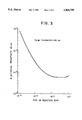
- FIG. 3 is a graph showing the correlation between the P/Si values and the resistivities
- FIG. 4 is a graph showing also the correlation between the P/Si values and the resistivities (when P/Si values increased);
- FIGS. 5A-5D are sectional views of a semiconductor wafer for showing fabrication steps thereof as a second embodiment according to tile invention.
- FIGS. 6A-6C are sectional views of a semiconductor wafer for showing fabrication steps thereof as a third embodiment according to the invention.
- FIGS. 1A to 1C are sectional views showing semiconductor wafers for describing a first embodiment of the invention.
- An aim of this embodiment is to obtain a low resistivity polycrystalline silicon Film having a very small thickness.
- an oxide film 12 of 100 nanometers in thick is formed on a p-type silicon substrate 11 with plane orientation ⁇ 100> and a resistivity of 1 ⁇ 10 -2 ⁇ .m.
- an oxide film 12 of 100 nanometers in thick is formed on a p-type silicon substrate 11 with plane orientation ⁇ 100> and a resistivity of 1 ⁇ 10 -2 ⁇ .m.
- a plurality of amorphous silicon thin films 13 doped with phosphorus (P) and having a thickness of 10 ⁇ 100 nanometers are formed using a usual batch type LP-CVD system with a resistive heating furnace.
- the reaction tube inner temperature is set to 470° C., and the pressure to 0.15 Torr.
- FIG. 2 shows the resistivity, plotted against the film thickness, of polycrystalline silicon thin film formed in a prior art example of the film formation method with P/Si set to 2.5 ⁇ 10 -2 .
- the resistivity is sufficiently low, i.e., 6 ⁇ 10 -6 ⁇ .m, for film thicknesses of 100 nanometers and above but, after the polycrystallization, the resistivity of tile polycrystalline silicon increases sharply as tile thickness of the amorphous silicon film is reduced to the neighborhood of 5O nanometers.
- FIG. 4 shows tile resistivities of polycrystalline silicon films with thicknesses of 18, 50 and 100 nanometers, plotted against the P/Si value for the film formation. which is increased from 2.0 ⁇ 10 -2 to five times thereof, i.e., 1 ⁇ 10 -1 .
- the resistivity is sufficiently reduced at P/Si of 2 ⁇ 10 -2 and is no longer reduced by further increasing the P/Si value.
- the resistivity is reduced from 1.5 ⁇ 10 -5 ⁇ .m to 1 ⁇ 10 -5 ⁇ .m by increasing tile P/Si value from 2 ⁇ 10 -2 to 5 ⁇ 10 -2 , the latter resistivity value being sufficiently low for the application of the film to various electrode materials. Further, by further increasing the P/Si value to 1 ⁇ 10 -1 , the resistivity is reduced down to a value comparable with that of the film with the thickness of 100 nanometers.
- FIG. 2 shows the resistivities, plotted against the film thickness, obtained with P/Si values of 1 ⁇ 10 -1 and 1.5 ⁇ 10 -1 together with those in the prior art example. As is seen, the resistivities can be reduced down to 1 ⁇ 10-5 ⁇ .m for film thicknesses down to about 30 nanometers with P/Si of 1 ⁇ 10 -1 and for film thicknesses down to about 20 nanometers with P/Si of 1.5 ⁇ 10 -1 .
- the P/Si value is set to be 5 ⁇ 10 -2 ⁇ 2 ⁇ 10 -1 . This is done so because if the value is above this range, excessive P atoms are introduced into the film resulting in an increase in the resistivities oppositely due to such causes as deterioration of the crystallinity or carrier impurity disturbance.
- this embodiment unlike in the prior art, it is possible to form a low resistivity polycrystalline silicon thin film with a thickness of 50 nanometers or below. While this embodiment relates to films doped with phosphorus (P), it is possible to obtain similar effects (i.e.. reduction in resistivity) in cases where other dopant impurities, such as arsenic (As) or boron (B), are introduced.
- dopant impurities such as arsenic (As) or boron (B)
- FIGS. 5A to 5D are sectional views showing semiconductor wafers for describing a second embodiment of the invention.
- the invention is applied to a buried contact material between a device active layer and an interconnect layer in various semiconductor devices.
- arsenic (As) is ion implanted into a p-type silicon substrate 21 of plane orientation ⁇ 100> from a principal surface to form an n + -type diffusion layer 22.
- a silicon oxide layer 23 with a thickness of 1 ⁇ m is formed over the entire surface, and then contact holes 28 with a diameter of 0.15 ⁇ m and a depth of 0.5 ⁇ are formed by photolithographic and ion etching processes.
- an amorphous silicon thin film is formed to a thickness of 100 nanometers over the entire surface while doping with phosphorus (P) with the P/Si value for the film formation set to 2.5 ⁇ 10 -2 (prior art example) and 1 ⁇ 10 -1 (embodiment), followed by a heat treatment at 850° C. for 30 minutes to crystallize the amorphous silicon thin film, thus forming a polycrystalline silicon thin film. Thereafter, the polycrystalline silicon thin film over the oxide film is removed by the ion etching process.
- P phosphorus
- isolation grooves 29 are formed to provide 1,000 polycrystalline silicon contact plug sections arranged in series.
- the contact resistance evaluation substrate With the contact resistance evaluation substrate thus produced, the contact resistance is measured.
- the resistance per contact is 450 ⁇ , which is extremely low compared to the resistance (800 ⁇ 1,000 ⁇ ) obtained in the case of the prior art method. It has been found that, by using the means of this embodiment, it is possible to form very small contacts with diameters of about 0.15 ⁇ m, which greatly contributes to the integration density increase of future semiconductor devices. Further, the same effect is obtainable by carrying out the film formation in the second embodiment with the P/SI value set to three times the prior art value.
- FIGS. 6A to 6C are sectional views showing semiconductor wafers for describing a third embodiment of the invention.
- the invention is applied to a memory device capacity electrode.
- arsenic (As) is ion implanted into a p-type single crystal silicon substrate with plane orientation ⁇ 100> from one principal surface thereof to form an n + -type diffusion layer 32. Then, a silicon oxide film 33 with a thickness of 1 ⁇ m is formed on the layer 32 by thermal oxidization, and a groove with a width of 1 ⁇ m is formed in the oxide film 33.
- an amorphous silicon thin film 35 is formed to thicknesses of 30 and 100 nanometers while doping with phosphorus (P) with the P/Si value for the film formation set to 2.5 ⁇ 10 -2 (prior art example) and 7.5 ⁇ 10 -2 (embodiment), followed by a heat treatment at 850° C. for 30 minutes for polycrystallization, thus forming a polycrystalline silicon thin film 35.
- P phosphorus
- the polycrystalline silicon thin film 35 is patterned to form an inner electrode 35A, and then a capacity insulation layer 36 is formed to a thickness of 5 nanometers.
- a capacity insulation layer 36 is formed to a thickness of 5 nanometers.
- an amorphous silicon film with a thickness of 150 nanometers is formed for an outer electrode 37, followed by a heat treatment at 850° C. for 30 minutes for polycrystallization.
- Table 1 shows the ratio (C/C O ) between the capacitance C when a voltage of +3 V is applied to tile inner electrode and tile capacitance C O in the neighborhood of zero bias, as determined by the high frequency C-V characteristics.
- the C/C O value is reduced from 0.98 to 0.85, thus indicating the spread of carrier depletion layer in the inner electrode polycrystalline silicon.
- the C/C O value is 0.94 and thus is not substantially reduced.
Abstract
Description
TABLE 1 ______________________________________ C-V CHARACTERISTICS Innerelectrode film thickness 100 nm 30 nm ______________________________________ P/Si (×10.sup.-2) 2.5 7.5 C/C.sub.o 0.98 0.85 0.94 ______________________________________
Claims (5)
Applications Claiming Priority (2)
| Application Number | Priority Date | Filing Date | Title |
|---|---|---|---|
| JP5-040800 | 1993-03-02 | ||
| JP4080093 | 1993-03-02 |
Publications (1)
| Publication Number | Publication Date |
|---|---|
| US5464795A true US5464795A (en) | 1995-11-07 |
Family
ID=12590713
Family Applications (1)
| Application Number | Title | Priority Date | Filing Date |
|---|---|---|---|
| US08/203,559 Expired - Fee Related US5464795A (en) | 1993-03-02 | 1994-03-01 | Method of forming polycrystalline silicon thin films for semiconductor devices |
Country Status (2)
| Country | Link |
|---|---|
| US (1) | US5464795A (en) |
| KR (1) | KR100250020B1 (en) |
Cited By (6)
| Publication number | Priority date | Publication date | Assignee | Title |
|---|---|---|---|---|
| EP0810640A1 (en) * | 1995-12-14 | 1997-12-03 | Seiko Epson Corporation | Thin film semiconductor device, method for manufacturing thin film semiconductor device, liquid crystal display, method for manufacturing liquid crystal display, electronic apparatus, method for manufacturing electronic apparatus, and method for depositing thin film |
| US5714415A (en) * | 1995-02-01 | 1998-02-03 | Nec Corporation | Method of forming thin semiconductor film |
| US5869389A (en) * | 1996-01-18 | 1999-02-09 | Micron Technology, Inc. | Semiconductor processing method of providing a doped polysilicon layer |
| US5955760A (en) * | 1996-08-09 | 1999-09-21 | Micron Technology, Inc. | Transistor device structures |
| US6177701B1 (en) * | 1996-01-04 | 2001-01-23 | Nec Corporation | Semiconductor device with resistor and fabrication method therof |
| US6391690B2 (en) | 1995-12-14 | 2002-05-21 | Seiko Epson Corporation | Thin film semiconductor device and method for producing the same |
Citations (17)
| Publication number | Priority date | Publication date | Assignee | Title |
|---|---|---|---|---|
| US4441249A (en) * | 1982-05-26 | 1984-04-10 | Bell Telephone Laboratories, Incorporated | Semiconductor integrated circuit capacitor |
| US4843022A (en) * | 1982-05-24 | 1989-06-27 | Semiconductor Energy Laboratory Co., Ltd. | Method of making fibrous silicon semiconductor by plasma CVD |
| US4877753A (en) * | 1986-12-04 | 1989-10-31 | Texas Instruments Incorporated | In situ doped polysilicon using tertiary butyl phosphine |
| US4891330A (en) * | 1987-07-27 | 1990-01-02 | Energy Conversion Devices, Inc. | Method of fabricating n-type and p-type microcrystalline semiconductor alloy material including band gap widening elements |
| US5064779A (en) * | 1989-02-08 | 1991-11-12 | President Of Kanazawa University | Method of manufacturing polycrystalline silicon film |
| US5096856A (en) * | 1988-03-01 | 1992-03-17 | Texas Instruments Incorporated | In-situ doped silicon using tertiary butyl phosphine |
| US5180690A (en) * | 1988-12-14 | 1993-01-19 | Energy Conversion Devices, Inc. | Method of forming a layer of doped crystalline semiconductor alloy material |
| US5198387A (en) * | 1989-12-01 | 1993-03-30 | Texas Instruments Incorporated | Method and apparatus for in-situ doping of deposited silicon |
| US5208479A (en) * | 1992-05-15 | 1993-05-04 | Micron Technology, Inc. | Method of increasing capacitance of polycrystalline silicon devices by surface roughening and polycrystalline silicon devices |
| US5225378A (en) * | 1990-11-16 | 1993-07-06 | Tokyo Electron Limited | Method of forming a phosphorus doped silicon film |
| US5227329A (en) * | 1990-08-31 | 1993-07-13 | Hitachi, Ltd. | Method of manufacturing semiconductor device |
| US5242855A (en) * | 1991-09-30 | 1993-09-07 | Nec Corporation | Method of fabricating a polycrystalline silicon film having a reduced resistivity |
| US5256566A (en) * | 1991-05-08 | 1993-10-26 | Texas Instruments Incorporated | Method for in-situ doping of deposited silicon |
| US5266504A (en) * | 1992-03-26 | 1993-11-30 | International Business Machines Corporation | Low temperature emitter process for high performance bipolar devices |
| US5310698A (en) * | 1990-12-21 | 1994-05-10 | Siemens Aktiengesellschaft | Process for producing an arsenic-doped smooth polycrystalline silicon layer for very large scale integrated circuits |
| US5370039A (en) * | 1992-03-24 | 1994-12-06 | Kirsching; Franz | Short travel high force transmitting pneumatic cylinder device |
| US5372958A (en) * | 1990-11-16 | 1994-12-13 | Seiko Epson Corporation | Process for fabricating a thin film semiconductor device |
-
1994
- 1994-02-28 KR KR1019940003752A patent/KR100250020B1/en not_active IP Right Cessation
- 1994-03-01 US US08/203,559 patent/US5464795A/en not_active Expired - Fee Related
Patent Citations (17)
| Publication number | Priority date | Publication date | Assignee | Title |
|---|---|---|---|---|
| US4843022A (en) * | 1982-05-24 | 1989-06-27 | Semiconductor Energy Laboratory Co., Ltd. | Method of making fibrous silicon semiconductor by plasma CVD |
| US4441249A (en) * | 1982-05-26 | 1984-04-10 | Bell Telephone Laboratories, Incorporated | Semiconductor integrated circuit capacitor |
| US4877753A (en) * | 1986-12-04 | 1989-10-31 | Texas Instruments Incorporated | In situ doped polysilicon using tertiary butyl phosphine |
| US4891330A (en) * | 1987-07-27 | 1990-01-02 | Energy Conversion Devices, Inc. | Method of fabricating n-type and p-type microcrystalline semiconductor alloy material including band gap widening elements |
| US5096856A (en) * | 1988-03-01 | 1992-03-17 | Texas Instruments Incorporated | In-situ doped silicon using tertiary butyl phosphine |
| US5180690A (en) * | 1988-12-14 | 1993-01-19 | Energy Conversion Devices, Inc. | Method of forming a layer of doped crystalline semiconductor alloy material |
| US5064779A (en) * | 1989-02-08 | 1991-11-12 | President Of Kanazawa University | Method of manufacturing polycrystalline silicon film |
| US5198387A (en) * | 1989-12-01 | 1993-03-30 | Texas Instruments Incorporated | Method and apparatus for in-situ doping of deposited silicon |
| US5227329A (en) * | 1990-08-31 | 1993-07-13 | Hitachi, Ltd. | Method of manufacturing semiconductor device |
| US5372958A (en) * | 1990-11-16 | 1994-12-13 | Seiko Epson Corporation | Process for fabricating a thin film semiconductor device |
| US5225378A (en) * | 1990-11-16 | 1993-07-06 | Tokyo Electron Limited | Method of forming a phosphorus doped silicon film |
| US5310698A (en) * | 1990-12-21 | 1994-05-10 | Siemens Aktiengesellschaft | Process for producing an arsenic-doped smooth polycrystalline silicon layer for very large scale integrated circuits |
| US5256566A (en) * | 1991-05-08 | 1993-10-26 | Texas Instruments Incorporated | Method for in-situ doping of deposited silicon |
| US5242855A (en) * | 1991-09-30 | 1993-09-07 | Nec Corporation | Method of fabricating a polycrystalline silicon film having a reduced resistivity |
| US5370039A (en) * | 1992-03-24 | 1994-12-06 | Kirsching; Franz | Short travel high force transmitting pneumatic cylinder device |
| US5266504A (en) * | 1992-03-26 | 1993-11-30 | International Business Machines Corporation | Low temperature emitter process for high performance bipolar devices |
| US5208479A (en) * | 1992-05-15 | 1993-05-04 | Micron Technology, Inc. | Method of increasing capacitance of polycrystalline silicon devices by surface roughening and polycrystalline silicon devices |
Non-Patent Citations (6)
| Title |
|---|
| "Deposition and electrical properties of in situ phosphorus-doped silicon films formed by low-pressure chemical vapor deposition", ]1987 American Institute for Physics, Arthur J. Learn et al. Mar. 1, 1987, pp. 1898-1904. |
| "Novel Highly Conductive Polycrystalline Silicon Films reducing Processing Temperature Down to 650° C.", Extended Abstracts of the 20th Conference on Solid State Device . . . T. Kobayashi et al. Tokyo 1988, pp. 57-60. |
| "Solubility of Implated Dopants in Polysilicon: Phosphorus and Arsenic", N. Lifshitz, Murray Hill, New Jersey, Solid-State Science and Technology, Dec. 1983, pp. 2464-2467. |
| Deposition and electrical properties of in situ phosphorus doped silicon films formed by low pressure chemical vapor deposition , 1987 American Institute for Physics, Arthur J. Learn et al. Mar. 1, 1987, pp. 1898 1904. * |
| Novel Highly Conductive Polycrystalline Silicon Films reducing Processing Temperature Down to 650 C. , Extended Abstracts of the 20th Conference on Solid State Device . . . T. Kobayashi et al. Tokyo 1988, pp. 57 60. * |
| Solubility of Implated Dopants in Polysilicon: Phosphorus and Arsenic , N. Lifshitz, Murray Hill, New Jersey, Solid State Science and Technology, Dec. 1983, pp. 2464 2467. * |
Cited By (9)
| Publication number | Priority date | Publication date | Assignee | Title |
|---|---|---|---|---|
| US5714415A (en) * | 1995-02-01 | 1998-02-03 | Nec Corporation | Method of forming thin semiconductor film |
| EP0810640A1 (en) * | 1995-12-14 | 1997-12-03 | Seiko Epson Corporation | Thin film semiconductor device, method for manufacturing thin film semiconductor device, liquid crystal display, method for manufacturing liquid crystal display, electronic apparatus, method for manufacturing electronic apparatus, and method for depositing thin film |
| EP0810640A4 (en) * | 1995-12-14 | 1999-06-16 | Seiko Epson Corp | Thin film semiconductor device, method for manufacturing thin film semiconductor device, liquid crystal display, method for manufacturing liquid crystal display, electronic apparatus, method for manufacturing electronic apparatus, and method for depositing thin film |
| US6391690B2 (en) | 1995-12-14 | 2002-05-21 | Seiko Epson Corporation | Thin film semiconductor device and method for producing the same |
| US6660572B2 (en) | 1995-12-14 | 2003-12-09 | Seiko Epson Corporation | Thin film semiconductor device and method for producing the same |
| US6177701B1 (en) * | 1996-01-04 | 2001-01-23 | Nec Corporation | Semiconductor device with resistor and fabrication method therof |
| US5869389A (en) * | 1996-01-18 | 1999-02-09 | Micron Technology, Inc. | Semiconductor processing method of providing a doped polysilicon layer |
| US6159828A (en) * | 1996-01-18 | 2000-12-12 | Micron Technology, Inc. | Semiconductor processing method of providing a doped polysilicon layer |
| US5955760A (en) * | 1996-08-09 | 1999-09-21 | Micron Technology, Inc. | Transistor device structures |
Also Published As
| Publication number | Publication date |
|---|---|
| KR940022681A (en) | 1994-10-21 |
| KR100250020B1 (en) | 2000-03-15 |
Similar Documents
| Publication | Publication Date | Title |
|---|---|---|
| US5242855A (en) | Method of fabricating a polycrystalline silicon film having a reduced resistivity | |
| US5714415A (en) | Method of forming thin semiconductor film | |
| US6066872A (en) | Semiconductor device and its fabricating method | |
| US5344796A (en) | Method for making polycrystalline silicon thin film | |
| US5318919A (en) | Manufacturing method of thin film transistor | |
| KR19990072884A (en) | Method for producing a polycrystalline silicon structure | |
| US5858852A (en) | Fabrication process of a stack type semiconductor capacitive element | |
| KR100299784B1 (en) | A method for forming a textured polysilicon layer, a substrate processing apparatus used to implement this method, and a semiconductor memory device | |
| JP2947828B2 (en) | Method for manufacturing semiconductor device | |
| US6326226B1 (en) | Method of crystallizing an amorphous film | |
| US5464795A (en) | Method of forming polycrystalline silicon thin films for semiconductor devices | |
| US5470780A (en) | Method of fabricating poly-silicon resistor | |
| US8102052B2 (en) | Process for the simultaneous deposition of crystalline and amorphous layers with doping | |
| JP3006396B2 (en) | Method of forming semiconductor thin film | |
| JPH0563439B2 (en) | ||
| JPH04245419A (en) | Manufacture of semiconductor substrate | |
| JP2707985B2 (en) | Method for manufacturing semiconductor device | |
| KR100196596B1 (en) | Method of forming thin semiconductor film | |
| KR100472855B1 (en) | Polycrystalline silicon thin film manufacturing method of semiconductor device | |
| JPH05299348A (en) | Forming method for polysrystalline silicon thin film | |
| JP3064363B2 (en) | Method of forming Si thin film | |
| KR960016220B1 (en) | Manufacturing method of semiconductor device | |
| JPH0653491A (en) | Fabrication of semiconductor device | |
| KR100342867B1 (en) | Method of forming gate electrode of semiconductor device including Co-silicide | |
| JP2812166B2 (en) | Method for manufacturing semiconductor device |
Legal Events
| Date | Code | Title | Description |
|---|---|---|---|
| AS | Assignment |
Owner name: NEC CORPORATION, JAPAN Free format text: ASSIGNMENT OF ASSIGNORS INTEREST;ASSIGNOR:OGURO, SHIZUO;REEL/FRAME:006902/0215 Effective date: 19940218 |
|
| FEPP | Fee payment procedure |
Free format text: PAYOR NUMBER ASSIGNED (ORIGINAL EVENT CODE: ASPN); ENTITY STATUS OF PATENT OWNER: LARGE ENTITY |
|
| FPAY | Fee payment |
Year of fee payment: 4 |
|
| AS | Assignment |
Owner name: NEC ELECTRONICS CORPORATION, JAPAN Free format text: ASSIGNMENT OF ASSIGNORS INTEREST;ASSIGNOR:NEC CORPORATION;REEL/FRAME:013758/0440 Effective date: 20021101 |
|
| FPAY | Fee payment |
Year of fee payment: 8 |
|
| REMI | Maintenance fee reminder mailed | ||
| LAPS | Lapse for failure to pay maintenance fees | ||
| LAPS | Lapse for failure to pay maintenance fees |
Free format text: PATENT EXPIRED FOR FAILURE TO PAY MAINTENANCE FEES (ORIGINAL EVENT CODE: EXP.); ENTITY STATUS OF PATENT OWNER: LARGE ENTITY |
|
| STCH | Information on status: patent discontinuation |
Free format text: PATENT EXPIRED DUE TO NONPAYMENT OF MAINTENANCE FEES UNDER 37 CFR 1.362 |
|
| FP | Lapsed due to failure to pay maintenance fee |
Effective date: 20071107 |