US5465375A - Multiprocessor system with cascaded modules combining processors through a programmable logic cell array - Google Patents
Multiprocessor system with cascaded modules combining processors through a programmable logic cell array Download PDFInfo
- Publication number
- US5465375A US5465375A US08/004,582 US458293A US5465375A US 5465375 A US5465375 A US 5465375A US 458293 A US458293 A US 458293A US 5465375 A US5465375 A US 5465375A
- Authority
- US
- United States
- Prior art keywords
- input
- data
- module
- memory
- processing unit
- Prior art date
- Legal status (The legal status is an assumption and is not a legal conclusion. Google has not performed a legal analysis and makes no representation as to the accuracy of the status listed.)
- Expired - Fee Related
Links
Images


Classifications
-
- G—PHYSICS
- G06—COMPUTING; CALCULATING OR COUNTING
- G06F—ELECTRIC DIGITAL DATA PROCESSING
- G06F15/00—Digital computers in general; Data processing equipment in general
- G06F15/16—Combinations of two or more digital computers each having at least an arithmetic unit, a program unit and a register, e.g. for a simultaneous processing of several programs
- G06F15/163—Interprocessor communication
- G06F15/173—Interprocessor communication using an interconnection network, e.g. matrix, shuffle, pyramid, star, snowflake
- G06F15/17337—Direct connection machines, e.g. completely connected computers, point to point communication networks
-
- G—PHYSICS
- G06—COMPUTING; CALCULATING OR COUNTING
- G06N—COMPUTING ARRANGEMENTS BASED ON SPECIFIC COMPUTATIONAL MODELS
- G06N3/00—Computing arrangements based on biological models
- G06N3/02—Neural networks
- G06N3/10—Interfaces, programming languages or software development kits, e.g. for simulating neural networks
-
- G—PHYSICS
- G06—COMPUTING; CALCULATING OR COUNTING
- G06V—IMAGE OR VIDEO RECOGNITION OR UNDERSTANDING
- G06V10/00—Arrangements for image or video recognition or understanding
- G06V10/40—Extraction of image or video features
- G06V10/44—Local feature extraction by analysis of parts of the pattern, e.g. by detecting edges, contours, loops, corners, strokes or intersections; Connectivity analysis, e.g. of connected components
- G06V10/443—Local feature extraction by analysis of parts of the pattern, e.g. by detecting edges, contours, loops, corners, strokes or intersections; Connectivity analysis, e.g. of connected components by matching or filtering
- G06V10/449—Biologically inspired filters, e.g. difference of Gaussians [DoG] or Gabor filters
- G06V10/451—Biologically inspired filters, e.g. difference of Gaussians [DoG] or Gabor filters with interaction between the filter responses, e.g. cortical complex cells
- G06V10/454—Integrating the filters into a hierarchical structure, e.g. convolutional neural networks [CNN]
-
- G—PHYSICS
- G06—COMPUTING; CALCULATING OR COUNTING
- G06V—IMAGE OR VIDEO RECOGNITION OR UNDERSTANDING
- G06V30/00—Character recognition; Recognising digital ink; Document-oriented image-based pattern recognition
- G06V30/40—Document-oriented image-based pattern recognition
- G06V30/42—Document-oriented image-based pattern recognition based on the type of document
- G06V30/424—Postal images, e.g. labels or addresses on parcels or postal envelopes
Definitions
- This invention relates to multiprocessor data processing systems in general.
- segmented (or pipeline) architectures this consists in breaking a task down into plural steps and in performing these steps independently by different processors. Every time an intermediary result is obtained after performance of a step, it is transmitted to the next processor and so on. When a step is completed, the processor in charge of performing it is freed and thus becomes available to process new data. Presupposing the respective durations of performance of the different steps to be substantially equal, the period required to obtain the final results is then the duration of performance of one step, and not the duration of performance of the task;
- SIMD Single Instruction, Multiple Data Stream
- MIMD Multiple Instruction, Multiple Data Stream
- Pending European Patent Application No. 433,142 filed Dec. 6, 1990 discloses an architecture of a multiprocessor data processing system in which the bus is shared between plural processor stages and is interfaced in each stage by a programmable LCA Logic Cell Array configurated into plural input/output means and a switching means.
- the main advantage of such an architecture is to dispense each processor from bus request and management tasks, the latter being carried out in the logic cells array associated with the processor. Nonetheless, this architecture is not optimal for the multiprocessor approach to scientific computation applications.
- Each processor is in fact entrusted with all the tasks to be performed (excepting management of the bus). Numerous multiprocessor applications require considerable computational means and a single unspecialized processor per stage restricts performances.
- the main object of this invention is to remedy the preceding disadvantages.
- Another object of this invention is to provide a data processing system optimizing the multiprocessor approach for each stage of the above-mentioned architecture.
- a multiprocessor data processing system embodying the invention including a plurality of cascaded modules.
- Each of the cascaded modules comprises
- Each of the cascaded modules further comprises;
- Each cascaded module further comprises;
- a first module bus for interconnecting the data processing unit, the first memory and the first input/output interface
- a second module bus for interconnecting the additional processing unit, the second memory and the fourth input/output interface.
- the second and third input/output interfaces in each of the modules are interconnected to the third input/output interface in the immediately adjacent downstream module and the second interface in the immediately adjacent upstream module by two intermodular buses, respectively.
- the processing and switching means is configurated for once and for all for a given application and, on the other hand, that several successive multiprocessor processings can be carried out by the processing units on a same data stream, the data already processed according to a first processing must be redistributed to the different modules for a next processing.
- the second and third input/output interfaces respectively in the programmable logic cell arrays of the last and first modules of the plurality of cascaded modules are connected by way of a feedback bus.
- the invention also relates to a data processing method implemented in a multiprocessor data processing system embodying the invention.
- the method comprises:
- an first step further consisting in loading a respective set of weights into the second memory of each of the cascaded modules via the communication network, and the input data into the first memory of the first module, and
- the second step consisting in carrying out partial processings on the input data in the additional processing unit of each cascaded module as a function of the respective set of matrix multiplication weights in order to determine partial data
- the third step consisting in downloading the partial data to any one of the programmable logic cell arrays or any one of the first and second memories in the cascaded modules via the intermodular buses and the feedback bus.
- FIG. 1 is a modelized diagram of an artificial neural network
- FIG. 2 is a diagram of a layered architecture of the modelized representation in FIG. 1;
- FIG. 3 is a block diagram of a multiprocessor data processing system with reconfigurable active bus according to the prior art
- FIGS. 4A and 4B are two respective block diagrams of two embodiments of a data processing system with specialized coprocessor embodying the invention.
- FIG. 5 is a diagram of feature maps obtained for successive processings in the layers of an artificial neural network
- FIG. 6 is a diagram of connections associated with synaptic weights between two adjacent layers of an artificial neural network
- FIG. 7 is a loading diagram of synaptic weights relating to two successive layers in a data processing system according to a preferred embodiment of the invention.
- FIG. 8 is a diagram of algorithms relating to the processing of the connections between two successive layers used in the system according to FIG. 7.
- the multiprocessor data processing system embodying the invention is described hereinafter for a particular embodiment concerning artificial neural networks.
- FIG. 1 A very general model representing a multilayer neural network is represented in FIG. 1: a certain number of elementary units . . . N i-1 , N i , N i+1 . . . called neurons and defined by their respective outputs . . . S i-1 , S i , S i+1 . . . constitute the nodes of the network.
- Each neuron N i is activated by a "potential" V i defined by the equation: ##EQU1## in which s j represents an output level of a neuron N j "connected " to the neuron N i , and W ji designates a synaptic weight of the connection between the neurons N j and N i . With this potential V i is associated the output level S i corresponding to the neuron N i defined by the relation:
- f is a non-linear function
- these neurons are not organized anarchically, but are grouped in layers in the form of "columns", connections between two adjacent layers being assigned to a particular function, as shown in FIG. 2.
- This figure represents n layers of superimposed neurons comprising two end layers LAYER 1 and LAYER N, and (N-2) hidden layers LAYER 2 to LAYER (N-1) included between the two end layers.
- the end layer 1 is commonly called the “retina " or "input layer " and receives an input vector whereas the end layer LAYER N, or output layer, produces a corresponding output vector.
- each neuron of a given layer n is connected to each of the neurons of the immediately adjacent upper layer (n+1), the integer n lying between 1 and N-1.
- a respective synaptic weight W is attributed to each of these connections.
- the neural network can be used for recognition of digits such as 0, 1, 2, . . . , 8, 9.
- the input vector is a block of digital pixels of a digitized image of a given digit written by any person whomsoever.
- a respective synaptic weight W deduced during a learning phase of the network To each connection between neurons is attributed a respective synaptic weight W deduced during a learning phase of the network. These synaptic weights correspond to values of coefficients of multiplication matrix applied to pixels of the image.
- the output layer LAYER N produces an output vector which is a binary information identifying the "recognized " digit.
- Outputs of neurons of a respective layer produce a feature map which has "filtered " features of the feature map produced from the outputs of the neurons of the lower adjacent layer.
- FIG. 3 A multiprocessor data processing system according to the prior art, as described in pending European Patent Application No. 433,142 filed Dec. 6, 1990, is shown in FIG. 3.
- the multiprocessor system comprises a plurality of modules in cascade, of which two adjacent modules M i and M i+1 are represented in FIG. 3.
- Each of the modules M i , M i+1 includes a processor PR i , PR i+1 , called a transputer, a RAM memory ME i , ME i+1 and a programmable logical cell array LCA i , LCA i+1 .
- the respective processors of the various modules are interconnected by means of an interprocessor communication network RC. This communication network RC notably ensures the transfer of monitoring/control information between processors.
- the processor PR i , the memory ME i and the logic cell array LCA i are interconnected by means of a respective module bus BM i .
- This module bus BM i is composed of three specialized elementary buses which are a data bus, an address bus and a control bus, and interconnects the processor, the memory and a first input/output interface in the logic cell array LCA i .
- Programmable logic cell arrays are known to those skilled in the art and are constituted by configurable logic, combinational and sequential circuits. The configuration of the programmable logic cell array (LCA i ) is set up by the module processor PR i .
- the programmable logic cell array is configurated into three input/output interfaces and a central data processing and switching circuit (hereinafter, the central circuit).
- the input/output interfaces notably carry out temporary data storage functions.
- the central circuit ensures data switching functions between the interfaces, and elementary processing functions (data format modification, encoding, precomputed functions) e.g. in pipeline mode.
- the first interface of the logic cell array constitutes the interface between the module bus BM i and the central circuit whereas the second and third interfaces respectively interface the central circuit with two intermodular buses BIM i and BIM i-1 .
- the buses BIM i and BIM 1-1 are then respectively connected with a third interface in the logic cell array of an immediately adjacent downstream module M i+1 and a second interface in the logic array of an immediately adjacent upstream module M i-1 .
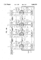
- FIG. 4A shows the first embodiment of a data processing system according to the invention for the carrying out of an artificial neural network within the scope e.g. of recognition of digits included between 0 and 9.
- the system comprises I modules 2 1 to 2 I in a cascaded architecture.
- Each module 2 i comprises a data processing unit in the form of a processor 20 i , a first RAM type memory 21 i , a programmable logic cell array 22 i , a second memory 23 i , and a digital signal processor constituting a coprocessor or dedicated specialized processing unit 24 i .
- the processor 20 i the memory 21 i and an input/output interface 221 i of the programmable logic cell array 22 i are interconnected by means of a common module bus 25 i .
- this common bus is constituted by the three elementary buses, i.e., address bus, data bus and control bus.
- the programmable logic cell array 22 i is programmed into four input/output interfaces 221 i , 222 i , 223 i and 224 i and a central data processing and switching circuit 220 i .
- the input/output interfaces 221 i to 224 i principally constitute temporary storage means or buffer means.
- the central circuit 220 i is configurated to switch data from and to the input/output interfaces 221 i to 224 i , and to conduct elementary processing of the data received through the input/output interfaces.
- the first input/output interface 221 i is connected to the module bus 25 i .
- This input/output interface 221 i is e.g. used for:
- DMA direct memory access
- the second and third interfaces 222 i and 223 i in the logic cell array 22 i of the ith module 2 i are respectively connected to a third input/output interface 223 i+1 of an immediately adjacent downstream module 2 i+1 , and a second input/output interface 222 i-1 of an immediately adjacent upstream module 2 i-1 .
- These connections are respectively made by means of two intermodular buses BI i (i+1) and BI.sub.(i-1)i.
- the I programmable logic cell arrays are thus cascaded by means of intermodular buses BI 12 , . . . , BI.sub.(I-1)I.
- the third input/output interface 223 1 of the first module 2 1 and the second interface 222 I of the I th module 2 I are connected by a feedback bus BR.
- the intermodular buses BI 12 to BI.sub.(I-1)I in series with the feedback bus BR thus constitute a ring.
- the second and third interfaces 222 i and 223 i can e.g. be used during a transmission of data between processors 20 i of non-adjacent modules and thus confer high-speed communication node functions upon the logic cell arrays 22 i .
- each module 2 i the digital signal processor 24 i , the second memory 23 i and the fourth input/output interface 224 i are interconnected by means of a common bus 26 i .
- FIG. 5 shows typical results obtained within the scope of artificial neural networks for the recognition of handwritten digits included between 0 and 9.
- Such an application can e.g. concern the recognition of zipcodes for "automated " postal distribution.
- the vertical ordinate axis relates to the numbers of neuron layers in an architecture such as that presented in reference to FIG. 2.
- the number of neuron layers is presupposed equal to 5.
- the input vector is an input block having (28 by 28) pixels representing any digit whatsoever, 0 in this instance, written by a person and digitized.
- the network is composed of 4,634 neurons.
- Each neuron in the input layer (LAYER 1), called retina, respectively receives a pixel of the input vector.
- the first hidden layer LAYER 2 is divided into 4 sub-layers of (24 by 24) neurons.
- Each neuron of each sub-layer receives (5 by 5) neighboring pixels of the input block after multiplication by a line matrix of respective synaptic weights. It is recalled that these synaptic weights are used for processing into matrix multiplication coefficients.
- Four blocks of (24 by 24) pixels are thus supplied by the respective outputs of the four sub-layers of neurons of LAYER 1.
- synaptic weights applied between the outputs of the neurons of the layer LAYER 1 and the four sub-layers of the second layer LAYER 2 relate to specific processings on the image of (28 by 28) input block pixels.
- Respective synaptic weights between the four sub-layers of LAYER 2 and four sub-layers of LAYER 3 relate to averaging and subsampling by two processings.
- Respective outputs of the neurons of the four sub-layers of LAYER 3 thus produce four image blocks of (12 by 12) pixels.
- each layer consists in extracting fundamental features from the digitalized (28 by 28) pixel block of a handwritten digit.
- an output layer of 10 neurons produces ten pixels in black and white, the rank of the sole white pixel produced by one of the ten neurons being representative of the "recognized " input digit subsequent to the various "digital filtering " steps respectively performed by the neuron layers.
- the neural network comprises three layers of 256, 40 and 10 neurons respectively.
- the neurons of the first layer, called input layer, and of the second layer each set up connections (each assigned to a respective synaptic weight) respectively with each of the neurons of the immediately adjacent upper layer, i.e., the second layer and the third layer, called output layer.
- each weight W jj of the rectangular matrix, j being included between 1 and J, and j' between 1 and J', corresponds to a value of a synaptic weight of the connection between a neuron of rank j and a neuron of rank j' of the two adjacent layers respectively.
- these synaptic weights for particular embodiments are obtained during a learning phase by a gradient back-propagation algorithm.
- this algorithm performs the recognition computations for synaptic weights given initially. The results of these computations are compared to expected recognition results. The weights are modified taking this comparison into account. After several iterations, the synaptic weights converge towards optimal recognition values. This learning phase is generally very costly as regards time.
- the system Prior to the operation of the system as an artificial neural network in the recognition mode, the system is initiated at the initiative of a master computer 1 connected to the first processor 20 1 .
- This initiation is established by the computer 1 via the interprocessor communication network RC.
- the initiation comprises:
- Each of the input vectors is e.g. supplied by the master computer 1 subsequent to a preprocessing (linear processing to normalize the 16 by 16 size of the initial blocks supplied by a video camera) on the initial blocks via the communication network RC.
- FIG. 8 The diagram of algorithms relating to a first processing of connections between first and second layers of neurons in FIG. 8 enables the operation of the multiprocessor data processing system embodying the invention as an artificial neural network to be grasped.
- Each of the "tables " in FIG. 8 relates to an algorithm performed by one or more of the processors 20 i , digital signal processors 24 i , or logic cell arrays 22 i of the system.
- the input data vector is initially loaded in the memory 21 1 .
- the processor 20 1 reads this vector in the memory 21 1 and writes it in the first input/output interface 221 1 of the programmable logic cell array 22 1 of the first module 2 1 .
- the central processing and switching circuit 220 1 of network 22 1 then switches this vector towards the second interface 222 1 and this second interface 222 1 retransmits it to the third interface 223 2 of the logic cell array 22 2 of the second module 2 2 and so on so forth.
- the vector is thus broadcast in the ring BI 12 to BI.sub.(I-1)I successively to the adjacent modules immediately above.
- Each of the central means of the networks switches and takes via the fourth interface 224 i the set of (16 by 16) pixels of the vector towards the memory 23 i associated with its digital signal processor 24 i .
- the data input vector used by each module 2 i in the configuration previously described is thus memorized in the respective memory 23 i associated with the digital signal processor 24 i .
- the first step (step 1) of the algorithm relating to each of the digital signal processors 24 i , with i lying between 1 and I, consists in computing the potential V i relating to the neurons attributed to the module 2 i , then in writing the potential thus computed in the input/output interface 224 i of the logic cell array 22 i of the same module 2 i .
- Each 220 i of the central circuit of the logic cell arrays configurated for this purpose gradually transmits the results of the potential computations V 1 to V i to the next logic cell array 22 i+1 until all the results V 1 to V I have been received by the third input/output interface 223 i of the logic cell array of the first module 2 1 via the feedback bus BR (step 2).
- the input/output interface 223 i of the first module 2 1 writes the potential computation results received in the memory 23 1 and alerts the digital signal processor 24 i (step 3).
- the processor 24 1 computes the value of the sigmoid function (non-linear f function based on hyperbolic tangent functions defined from the model initially presented in the specification) for each "pixel " or neuron potential V i produced by the processors 24 i (step 5) for obtaining the output levels of all the neurons in the second layer for this first processing.
- each digital signal processor 24 i writes the computed potentials specific to the four neurons of the second layer which it simulates in this first processing, in the associated memory 23 i , the processors 20 1 to 20 I then read the neuron potentials respectively memorized in the memories 23 1 to 23 I when all the potentials have been computed (step 2').
- two processings relating to the first and second layers and to the second and third layers are provided.
- the outputs of the neurons in the second layer of the chosen configuration memorized in the memory 23 i are reprocessed by the digital signal processors 24 1 to 24 I for new potential computations after broadcasting in the ring of the neuron outputs as computed during the first processing.
- an additional module 2 0 to the initial modules 2 1 to 2 I is proposed upstream of the latter.
- This additional module comprises a processor 20 0 , a memory 21 0 and a programmable logic cell array 22 0 .
- This module is provided in order to directly inject the pixel images to be processed into an input/output interface 223 0 of the programmable logic cell array 22 0 .
- This injection enables an increase of the flow of images to be processed since the images then do not transit via the master computer 1 and, furthermore, do not require utilisation of the communication network RC.
- a data (images) acquiring system such as a video camera or scanner (not shown), is then directly connected to the third input/output interface 223 0 of the programmable array 22 0 of the additional module 2 0 via a bus BI.
- the memory 21 0 , the processor 20 0 and a first input/output interface 221 0 of the programmable logic cell array 22 0 in the additional module 2 0 are interconnected in identical manner to the interconnections in the other modules 2 1 to 2 I , by means of a bus 25 0 .
- the images to be processed which are injected via a bus in the third input/output interface 223 0 of the programmable logic cell array 22 0 can undergo a first preprocessing (16 by 16 formatting), in a processing and switching circuit 220 0 of the logic cell array 22 0 by programming of the latter.
- the second interface 222 0 is connected to the third interface 223 1 of the first 2 1 of the modules in cascade 2 1 to 2 I via an additional intermodular bus BI 01 .
- a feedback bus BR can also be provided.
- the latter interconnects the second input/output interface 222 I of the programmable logic cell array 22 I of the last module 2 I to the fourth input/output interface 224 0 of the logic cell array 22 0 of the additional module.
- a recognition of a digitized handwritten digit in (16 by 16)pixels by the data processing system embodying the invention simulating 10,640 neurons requires 175 ⁇ s. Durations of the order of a tenth of millisecond are usually required for conventional systems.
Abstract
In a multiprocessor data processing system, modules are cascaded by means of intermodule buses. Each module comprises a data processing unit, a first memory, a logic cell array programmable into four input/output interfaces, a second memory and a specialized processing unit such as a digital signal processor (DSP). A first interface, the first memory and the data processing unit are interconnected by a module bus. A fourth interface, the second memory and the specialized processing unit are interconnected by another module bus. A feedback bus connects the second and third interfaces in the last and first modules for constituting a ring. Such a system is particularly intended for image recognition, such as digitalized handwritten digits for postal distribution.
Description
1. Field of the Invention
This invention relates to multiprocessor data processing systems in general.
2. Description of the Prior Art
The increasingly greater computational throughput requirements in data processing systems for applications such as image processing or scientific computation, have led computer designers to introduce new processor architectures: parallel architectures. Three basic principles are used for introducing this parallelism in the new achitectures. The distinction is made between:
segmented (or pipeline) architectures: this consists in breaking a task down into plural steps and in performing these steps independently by different processors. Every time an intermediary result is obtained after performance of a step, it is transmitted to the next processor and so on. When a step is completed, the processor in charge of performing it is freed and thus becomes available to process new data. Presupposing the respective durations of performance of the different steps to be substantially equal, the period required to obtain the final results is then the duration of performance of one step, and not the duration of performance of the task;
array processor architectures or SIMD (Single Instruction, Multiple Data Stream) architectures. In this type of architecture, the increase in computational throughput is obtained by having the same instruction performed by a large number of identical processing units. This type of architecture is particularly well suited to vectorial processing; and
multiprocessor architectures or MIMD (Multiple Instruction, Multiple Data Stream) architectures. In such an architecture, several processors perform respective streams of instructions independently of one another. Communication between the processors is ensured either by a common memory and/or by a network interconnecting the processors.
Pending European Patent Application No. 433,142 filed Dec. 6, 1990 discloses an architecture of a multiprocessor data processing system in which the bus is shared between plural processor stages and is interfaced in each stage by a programmable LCA Logic Cell Array configurated into plural input/output means and a switching means. The main advantage of such an architecture is to dispense each processor from bus request and management tasks, the latter being carried out in the logic cells array associated with the processor. Nonetheless, this architecture is not optimal for the multiprocessor approach to scientific computation applications. Each processor is in fact entrusted with all the tasks to be performed (excepting management of the bus). Numerous multiprocessor applications require considerable computational means and a single unspecialized processor per stage restricts performances.
The main object of this invention is to remedy the preceding disadvantages.
Another object of this invention is to provide a data processing system optimizing the multiprocessor approach for each stage of the above-mentioned architecture.
Accordingly, there is provided a multiprocessor data processing system embodying the invention including a plurality of cascaded modules.
Each of the cascaded modules comprises
a data processing unit connected to other data processing units in immediately adjacent downstream and upstream modules by way of a communication network. Each of the cascaded modules further comprises;
a first memory,
an additional processing unit,
a second memory,
a logic programmable cell array. The programmable logic cell array is configurable into first, second, third and fourth input/output interfaces for temporarily memorizing data into memorized data, and into a central processing and switching circuit for processing the memorized data into processed data and switching the processed data towards one of the input/output interfaces. Each cascaded module further comprises;
a first module bus for interconnecting the data processing unit, the first memory and the first input/output interface, and
a second module bus for interconnecting the additional processing unit, the second memory and the fourth input/output interface.
The second and third input/output interfaces in each of the modules are interconnected to the third input/output interface in the immediately adjacent downstream module and the second interface in the immediately adjacent upstream module by two intermodular buses, respectively.
According to another embodiment, given that, on the one hand, the processing and switching means is configurated for once and for all for a given application and, on the other hand, that several successive multiprocessor processings can be carried out by the processing units on a same data stream, the data already processed according to a first processing must be redistributed to the different modules for a next processing. In this case, the second and third input/output interfaces respectively in the programmable logic cell arrays of the last and first modules of the plurality of cascaded modules are connected by way of a feedback bus.
The invention also relates to a data processing method implemented in a multiprocessor data processing system embodying the invention. The method comprises:
an first step further consisting in loading a respective set of weights into the second memory of each of the cascaded modules via the communication network, and the input data into the first memory of the first module, and
at least one set of second and third steps,
the second step consisting in carrying out partial processings on the input data in the additional processing unit of each cascaded module as a function of the respective set of matrix multiplication weights in order to determine partial data, and
the third step consisting in downloading the partial data to any one of the programmable logic cell arrays or any one of the first and second memories in the cascaded modules via the intermodular buses and the feedback bus.
Further features and advantages of the invention will be apparent from the following particular description of two preferred embodiments of this invention with reference to the corresponding accompanying drawings in which:
FIG. 1 is a modelized diagram of an artificial neural network;
FIG. 2 is a diagram of a layered architecture of the modelized representation in FIG. 1;
FIG. 3 is a block diagram of a multiprocessor data processing system with reconfigurable active bus according to the prior art;
FIGS. 4A and 4B are two respective block diagrams of two embodiments of a data processing system with specialized coprocessor embodying the invention;
FIG. 5 is a diagram of feature maps obtained for successive processings in the layers of an artificial neural network;
FIG. 6 is a diagram of connections associated with synaptic weights between two adjacent layers of an artificial neural network;
FIG. 7 is a loading diagram of synaptic weights relating to two successive layers in a data processing system according to a preferred embodiment of the invention; and
FIG. 8 is a diagram of algorithms relating to the processing of the connections between two successive layers used in the system according to FIG. 7.
The multiprocessor data processing system embodying the invention is described hereinafter for a particular embodiment concerning artificial neural networks.
A very general model representing a multilayer neural network is represented in FIG. 1: a certain number of elementary units . . . Ni-1, Ni, Ni+1 . . . called neurons and defined by their respective outputs . . . Si-1, Si, Si+1 . . . constitute the nodes of the network. Each neuron Ni is activated by a "potential" Vi defined by the equation: ##EQU1## in which sj represents an output level of a neuron Nj "connected " to the neuron Ni, and Wji designates a synaptic weight of the connection between the neurons Nj and Ni. With this potential Vi is associated the output level Si corresponding to the neuron Ni defined by the relation:
S.sub.i (t+Δt)=f(V.sub.i (t))
in which f is a non-linear function.
In practice and by analogy with the human brain, these neurons are not organized anarchically, but are grouped in layers in the form of "columns", connections between two adjacent layers being assigned to a particular function, as shown in FIG. 2. This figure represents n layers of superimposed neurons comprising two end layers LAYER 1 and LAYER N, and (N-2) hidden layers LAYER 2 to LAYER (N-1) included between the two end layers. The end layer 1 is commonly called the "retina " or "input layer " and receives an input vector whereas the end layer LAYER N, or output layer, produces a corresponding output vector. In this representation, each neuron of a given layer n is connected to each of the neurons of the immediately adjacent upper layer (n+1), the integer n lying between 1 and N-1. As specified, with reference to FIG. 1, a respective synaptic weight W is attributed to each of these connections.
In practice, and by way of an example, the neural network can be used for recognition of digits such as 0, 1, 2, . . . , 8, 9. In this case, the input vector is a block of digital pixels of a digitized image of a given digit written by any person whomsoever. To each connection between neurons is attributed a respective synaptic weight W deduced during a learning phase of the network. These synaptic weights correspond to values of coefficients of multiplication matrix applied to pixels of the image. The output layer LAYER N produces an output vector which is a binary information identifying the "recognized " digit. Outputs of neurons of a respective layer produce a feature map which has "filtered " features of the feature map produced from the outputs of the neurons of the lower adjacent layer. Each step in the implementation of this model for the multiprocessor data processing system embodying the invention will be described in greater detail further on.
A multiprocessor data processing system according to the prior art, as described in pending European Patent Application No. 433,142 filed Dec. 6, 1990, is shown in FIG. 3. The multiprocessor system comprises a plurality of modules in cascade, of which two adjacent modules Mi and Mi+1 are represented in FIG. 3. Each of the modules Mi, Mi+1 includes a processor PRi, PRi+1, called a transputer, a RAM memory MEi, MEi+1 and a programmable logical cell array LCAi, LCAi+1. The respective processors of the various modules are interconnected by means of an interprocessor communication network RC. This communication network RC notably ensures the transfer of monitoring/control information between processors. For a given module Mi, the processor PRi, the memory MEi and the logic cell array LCAi are interconnected by means of a respective module bus BMi. This module bus BMi is composed of three specialized elementary buses which are a data bus, an address bus and a control bus, and interconnects the processor, the memory and a first input/output interface in the logic cell array LCAi. Programmable logic cell arrays (LCA) are known to those skilled in the art and are constituted by configurable logic, combinational and sequential circuits. The configuration of the programmable logic cell array (LCAi) is set up by the module processor PRi.
According to the above-mentioned architecture, the programmable logic cell array is configurated into three input/output interfaces and a central data processing and switching circuit (hereinafter, the central circuit). The input/output interfaces notably carry out temporary data storage functions. The central circuit ensures data switching functions between the interfaces, and elementary processing functions (data format modification, encoding, precomputed functions) e.g. in pipeline mode. The first interface of the logic cell array constitutes the interface between the module bus BMi and the central circuit whereas the second and third interfaces respectively interface the central circuit with two intermodular buses BIMi and BIMi-1. The buses BIMi and BIM1-1 are then respectively connected with a third interface in the logic cell array of an immediately adjacent downstream module Mi+1 and a second interface in the logic array of an immediately adjacent upstream module Mi-1.
The introduction of a programmable logic cell array in each module of such a multiprocessor architecture is particularly interesting in that its induces a fine grain of parallelism between modules while assigning the low-level tasks (access to the intermodular bus, elementary functions) to the logic array LCAi.
FIG. 4A shows the first embodiment of a data processing system according to the invention for the carrying out of an artificial neural network within the scope e.g. of recognition of digits included between 0 and 9. The system comprises I modules 21 to 2I in a cascaded architecture.
Each module 2i, i being an integer varying between 1 and I, comprises a data processing unit in the form of a processor 20i, a first RAM type memory 21i, a programmable logic cell array 22i, a second memory 23i, and a digital signal processor constituting a coprocessor or dedicated specialized processing unit 24i. Within the module 2i, the processor 20i, the memory 21i and an input/output interface 221i of the programmable logic cell array 22i are interconnected by means of a common module bus 25i. Typically, this common bus is constituted by the three elementary buses, i.e., address bus, data bus and control bus.
By comparison with the foregoing description in reference to the prior art according to FIG. 3, the programmable logic cell array 22i is programmed into four input/ output interfaces 221i, 222i, 223i and 224i and a central data processing and switching circuit 220i. According to this embodiment, the input/output interfaces 221i to 224i principally constitute temporary storage means or buffer means. The central circuit 220i is configurated to switch data from and to the input/output interfaces 221i to 224i, and to conduct elementary processing of the data received through the input/output interfaces.
The first input/output interface 221i is connected to the module bus 25i. This input/output interface 221i is e.g. used for:
temporary storage of data transmitted by the processor 20i in order to free the latter for other tasks; and
direct memory access (DMA) to the memory 21i connected to processor 20i by means of the logic cell array 22i.
The second and third interfaces 222i and 223i in the logic cell array 22i of the ith module 2i are respectively connected to a third input/output interface 223i+1 of an immediately adjacent downstream module 2i+1, and a second input/output interface 222i-1 of an immediately adjacent upstream module 2i-1. These connections are respectively made by means of two intermodular buses BIi(i+1) and BI.sub.(i-1)i. The I programmable logic cell arrays are thus cascaded by means of intermodular buses BI12, . . . , BI.sub.(I-1)I. According to this first preferred embodiment, the third input/output interface 2231 of the first module 21 and the second interface 222I of the Ith module 2I are connected by a feedback bus BR.
The intermodular buses BI12 to BI.sub.(I-1)I in series with the feedback bus BR thus constitute a ring. The second and third interfaces 222i and 223i can e.g. be used during a transmission of data between processors 20i of non-adjacent modules and thus confer high-speed communication node functions upon the logic cell arrays 22i.
In each module 2i, the digital signal processor 24i, the second memory 23i and the fourth input/output interface 224i are interconnected by means of a common bus 26i.
With reference to FIGS. 5, 6, 7 and 8, the operation of the data processing system embodying the invention will now be described for the preferred embodiment concerning artificial neural networks.
FIG. 5 shows typical results obtained within the scope of artificial neural networks for the recognition of handwritten digits included between 0 and 9. Such an application can e.g. concern the recognition of zipcodes for "automated " postal distribution. In the diagram in FIG. 5, the vertical ordinate axis relates to the numbers of neuron layers in an architecture such as that presented in reference to FIG. 2. In this diagram, the number of neuron layers is presupposed equal to 5. The input vector is an input block having (28 by 28) pixels representing any digit whatsoever, 0 in this instance, written by a person and digitized. The network is composed of 4,634 neurons.
Each neuron in the input layer (LAYER 1), called retina, respectively receives a pixel of the input vector. The first hidden layer LAYER 2 is divided into 4 sub-layers of (24 by 24) neurons. Each neuron of each sub-layer receives (5 by 5) neighboring pixels of the input block after multiplication by a line matrix of respective synaptic weights. It is recalled that these synaptic weights are used for processing into matrix multiplication coefficients. Four blocks of (24 by 24) pixels are thus supplied by the respective outputs of the four sub-layers of neurons of LAYER 1.
The synaptic weights applied between the outputs of the neurons of the layer LAYER 1 and the four sub-layers of the second layer LAYER 2 relate to specific processings on the image of (28 by 28) input block pixels. Respective synaptic weights between the four sub-layers of LAYER 2 and four sub-layers of LAYER 3 relate to averaging and subsampling by two processings. Respective outputs of the neurons of the four sub-layers of LAYER 3 thus produce four image blocks of (12 by 12) pixels.
Details of LAYER 3 and LAYER 4 will not be provided. It should nevertheless be remarked that the role of each layer consists in extracting fundamental features from the digitalized (28 by 28) pixel block of a handwritten digit. As shown in FIG. 5, an output layer of 10 neurons produces ten pixels in black and white, the rank of the sole white pixel produced by one of the ten neurons being representative of the "recognized " input digit subsequent to the various "digital filtering " steps respectively performed by the neuron layers.
In reference to FIGS. 6, 7 and 8, the installation of an artificial neural network in the multiprocessor data processing system embodying the invention, as shown in FIG. 4A, will now be described. According to this preferred embodiment, the neural network comprises three layers of 256, 40 and 10 neurons respectively. The neurons of the first layer, called input layer, and of the second layer each set up connections (each assigned to a respective synaptic weight) respectively with each of the neurons of the immediately adjacent upper layer, i.e., the second layer and the third layer, called output layer. The input vector is a block of (16×16)=256 pixels of a digitalized image of a handwritten digit included between 0 and 9.
As shown in FIG. 6, all the connections assigned to respective synaptic weights between two adjacent layers respectively having J and J' neurons are fully defined by a single rectangular matrix of size (J×J'). Each weight Wjj, of the rectangular matrix, j being included between 1 and J, and j' between 1 and J', corresponds to a value of a synaptic weight of the connection between a neuron of rank j and a neuron of rank j' of the two adjacent layers respectively.
In compliance with the preferred embodiment, two respective matrices of (J×J')=(256×40) and (J×J')=(4×10) synaptic weights between the first and second layers and between the second and third layers are then used, i.e., a total of 10,640 weights or connections.
For indicative purposes, these synaptic weights for particular embodiments (recognition of digits, . . . ) are obtained during a learning phase by a gradient back-propagation algorithm. Summarily, this algorithm performs the recognition computations for synaptic weights given initially. The results of these computations are compared to expected recognition results. The weights are modified taking this comparison into account. After several iterations, the synaptic weights converge towards optimal recognition values. This learning phase is generally very costly as regards time.
According to the first preferred embodiment, the data processing system embodying the invention (FIG. 4A) comprises I =10 modules 21 to 210. In a first step, as shown schematically in FIG. 7, each module 2i, i lying between 1 and 10, is assigned to the processing relating to all the connections between the input layer and respectively one of the ten quadruplets of neurons in the second layer (4×10=40). The matrix computations: ##EQU2## where k varies between 1 and J=(16×16) and p varies between 1 and J'=40,
are carried out by the same digital signal processor for four set values of the index p, and therefore in relation to the four neurons of a respective quadruplet.
One advantage of the invention is that these matrix multiplications are performed by the digital signal processors 24i to 24I=10.
Further to this first processing (connections between the first and second layers), each digital signal processor 24i to 2410 is assigned to the processing of the matrix multiplications relating to the connections between the neurons of the second layer and a respective neuron of the third layer, called output layer (1×10=10).
The utilisation of a digital signal processor or specialized coprocessor 24i frees the processor 20i which can perform other tasks.
In reference to FIGS. 8 and 4A, the implementation and operation of an artificial neural network in the multiprocessor data processing system embodying the invention will now be described.
Prior to the operation of the system as an artificial neural network in the recognition mode, the system is initiated at the initiative of a master computer 1 connected to the first processor 201. This initiation is established by the computer 1 via the interprocessor communication network RC. The initiation comprises:
with regard to each processor 201 to 2010 :
loading of an operating program in the respective memory 211 to 2110 via the bus 251 to 2510 ;
configurating of the associated logic cell array 221 to 2210 ;
loading of programs (matrix multiplication, . . . ) relating to the operation of the digital signal processor 241 to 2410 in the associated memory 231 to 2310 via the network 221 to 2210, and
loading of a respective set of synaptic weights such as previously described and relating to the digital signal processor 241 to 2410, in the associated memory 231 to 2310 ;
as well as the loading of the first input vector constituting input data e1 to eJ to be recognized by processing (block of 16 by 16 pixels), in the memory 211 of the processor 201 of the first module 21.
In the case of a sequential processing of plural input data vectors to be recognized, the latter are memorized as they become available in the memory 211 connected to the processor of the first module 21. Each of the input vectors is e.g. supplied by the master computer 1 subsequent to a preprocessing (linear processing to normalize the 16 by 16 size of the initial blocks supplied by a video camera) on the initial blocks via the communication network RC.
The diagram of algorithms relating to a first processing of connections between first and second layers of neurons in FIG. 8 enables the operation of the multiprocessor data processing system embodying the invention as an artificial neural network to be grasped. Each of the "tables " in FIG. 8 relates to an algorithm performed by one or more of the processors 20i, digital signal processors 24i, or logic cell arrays 22i of the system.
It has been seen previously that the input data vector is initially loaded in the memory 211. The processor 201 reads this vector in the memory 211 and writes it in the first input/output interface 2211 of the programmable logic cell array 221 of the first module 21. The central processing and switching circuit 2201 of network 221 then switches this vector towards the second interface 2221 and this second interface 2221 retransmits it to the third interface 2232 of the logic cell array 222 of the second module 22 and so on so forth. The vector is thus broadcast in the ring BI12 to BI.sub.(I-1)I successively to the adjacent modules immediately above. Each of the central means of the networks switches and takes via the fourth interface 224i the set of (16 by 16) pixels of the vector towards the memory 23i associated with its digital signal processor 24i. The data input vector used by each module 2i in the configuration previously described is thus memorized in the respective memory 23i associated with the digital signal processor 24i.
The first step (step 1) of the algorithm relating to each of the digital signal processors 24i, with i lying between 1 and I, consists in computing the potential Vi relating to the neurons attributed to the module 2i, then in writing the potential thus computed in the input/output interface 224i of the logic cell array 22i of the same module 2i. Each 220i of the central circuit of the logic cell arrays configurated for this purpose gradually transmits the results of the potential computations V1 to Vi to the next logic cell array 22i+1 until all the results V1 to VI have been received by the third input/output interface 223i of the logic cell array of the first module 21 via the feedback bus BR (step 2).
Then the input/output interface 223i of the first module 21 writes the potential computation results received in the memory 231 and alerts the digital signal processor 24i (step 3). The processor 241 computes the value of the sigmoid function (non-linear f function based on hyperbolic tangent functions defined from the model initially presented in the specification) for each "pixel " or neuron potential Vi produced by the processors 24i (step 5) for obtaining the output levels of all the neurons in the second layer for this first processing. At the same time and as each digital signal processor 24i writes the computed potentials specific to the four neurons of the second layer which it simulates in this first processing, in the associated memory 23i, the processors 201 to 20I then read the neuron potentials respectively memorized in the memories 231 to 23I when all the potentials have been computed (step 2').
According to the embodiment, two processings relating to the first and second layers and to the second and third layers are provided. In this way the outputs of the neurons in the second layer of the chosen configuration memorized in the memory 23i are reprocessed by the digital signal processors 241 to 24I for new potential computations after broadcasting in the ring of the neuron outputs as computed during the first processing.
According to the second embodiment shown in FIG. 4B, the addition of an additional module 20 to the initial modules 21 to 2I is proposed upstream of the latter. This additional module comprises a processor 200, a memory 210 and a programmable logic cell array 220. This module is provided in order to directly inject the pixel images to be processed into an input/output interface 2230 of the programmable logic cell array 220. This injection enables an increase of the flow of images to be processed since the images then do not transit via the master computer 1 and, furthermore, do not require utilisation of the communication network RC. A data (images) acquiring system, such as a video camera or scanner (not shown), is then directly connected to the third input/output interface 2230 of the programmable array 220 of the additional module 20 via a bus BI. The memory 210, the processor 200 and a first input/output interface 2210 of the programmable logic cell array 220 in the additional module 20 are interconnected in identical manner to the interconnections in the other modules 21 to 2I, by means of a bus 250. The images to be processed which are injected via a bus in the third input/output interface 2230 of the programmable logic cell array 220 can undergo a first preprocessing (16 by 16 formatting), in a processing and switching circuit 2200 of the logic cell array 220 by programming of the latter. The second interface 2220 is connected to the third interface 2231 of the first 21 of the modules in cascade 21 to 2I via an additional intermodular bus BI01.
For identical reasons to those of the first embodiment, a feedback bus BR can also be provided. The latter interconnects the second input/output interface 222I of the programmable logic cell array 22I of the last module 2I to the fourth input/output interface 2240 of the logic cell array 220 of the additional module.
For indicative purposes, a recognition of a digitized handwritten digit in (16 by 16)pixels by the data processing system embodying the invention simulating 10,640 neurons requires 175 μs. Durations of the order of a tenth of millisecond are usually required for conventional systems.
Claims (2)
1. An input data processing method implemented in a multiprocessor data processing system,
said multiprocessor data processing system comprising a plurality of cascaded modules, each of said cascaded modules comprising:
a data processing unit connected to other data processing units in immediately adjacent downstream and upstream modules by means of a communication network,
a first memory for storing data,
an additional processing unit,
a second memory for storing data associated with said additional processing unit,
a programmable logic cell array configurable into first, second, third and fourth input/output interfacing means for temporarily memorizing data into memorized data, and into a central processing and switching means for processing said memorized data into processed data and switching said processed data towards one of said input/output interfacing means,
a first module bus for interconnecting said data processing unit, said first memory and said first input/output interfacing means, and
a second module bus for interconnecting said additional processing unit, said second memory and said fourth input/output interfacing means,
said second and third input/output interfacing means in said each of said cascaded modules being interconnected to the third input/output interfacing means in said immediately adjacent upstream module and the second input/output interfacing means in said immediately adjacent downstream module, by two intermodular buses, respectively,
said second and third input/output interfacing means respectively in said programmable logic cell array of a last module and a first module in said plurality of said cascaded modules being connected by means of a feedback bus,
said input data processing method comprising:
a first step further consisting in loading a respective set of matrix multiplication weights into said second memory of each of said cascaded modules via said communication network and said input data into said first memory of said first module, and
at least one set of second and third steps in each of said cascaded modules,
said second step consisting in carrying out partial processings on said input data in said additional processing unit of said each cascaded module as a function of said respective set of matrix multiplication weights for determining partial data, and
said third step consisting in downloading said partial data to any one of said programmable logic cell arrays or any one of said first and second memories in said cascaded modules via said intermodular buses and said feedback bus.
2. An input data processing method implemented in a multiprocessor data processing system,
said multiprocessor data processing system comprising a plurality of cascaded modules, each of said cascaded modules comprising:
a data processing unit connected to other data processing units in immediately adjacent downstream and upstream modules by means of a communication network,
a first memory for storing data,
an additional processing unit,
a second memory for storing data associated with said additional processing unit,
a programmable logic cell array configurable into first, second, third and fourth input/output interfacing means for temporarily memorizing data into memorized data, and into a central processing and switching means for processing said memorized data into processed data and switching said processed data towards one of said input/output interfacing means,
a first module bus for interconnecting said data processing unit, said first memory and said first input/output interfacing means,
a second module bus for interconnecting said additional processing unit, said second memory and said fourth input/output interfacing means,
said second and third input/output interfacing means in said each of said cascaded modules being interconnected to the third input/output interfacing means in said immediately adjacent downstream module and the second input/output interfacing means in said immediately adjacent upstream module by two intermodular buses, respectively, and
an additional module, a data acquiring means and an additional intermodular bus,
said additional module including a data processing unit, a first memory and a programmable logic cell array configurable into first, second, third and fourth input/output interfacing means,
said acquiring means being interconnected with said third input/output interfacing means in said programmable logic cell array of said additional module,
said additional intermodular bus interconnecting said second input/output interfacing means in said programmable logic cell array of said additional module and said third input/output interfacing means in a first of said plurality of said cascaded modules,
wherein said second input/output interfacing means in said programmable logic cell array of the last module in said plurality of said cascaded modules and said fourth input/output interfacing means in said additional module are connected by means of a feedback bus,
said input data processing method comprising:
a first step further consisting in loading a respective set of matrix multiplication weights into said second memory of each of said cascaded modules via said communication network and said input data into said first memory of said first module, and
at least one set of second and third steps in each of said cascaded modules,
said second step consisting in carrying out partial processings on said input data in said additional processing unit of said each cascaded module as a function of said respective set of matrix multiplication weights for determining partial data, and
said third step consisting in downloading said partial data to any one of said programmable logic cell arrays or any one of said first and second memories in said cascaded modules via said intermodular buses and said feedback bus.
Applications Claiming Priority (2)
| Application Number | Priority Date | Filing Date | Title |
|---|---|---|---|
| FR9200312A FR2686175B1 (en) | 1992-01-14 | 1992-01-14 | MULTIPROCESSOR DATA PROCESSING SYSTEM. |
| FR9200312 | 1992-01-14 |
Publications (1)
| Publication Number | Publication Date |
|---|---|
| US5465375A true US5465375A (en) | 1995-11-07 |
Family
ID=9425613
Family Applications (1)
| Application Number | Title | Priority Date | Filing Date |
|---|---|---|---|
| US08/004,582 Expired - Fee Related US5465375A (en) | 1992-01-14 | 1993-01-14 | Multiprocessor system with cascaded modules combining processors through a programmable logic cell array |
Country Status (5)
| Country | Link |
|---|---|
| US (1) | US5465375A (en) |
| EP (1) | EP0552074B1 (en) |
| JP (1) | JPH0612393A (en) |
| DE (1) | DE69300041T2 (en) |
| FR (1) | FR2686175B1 (en) |
Cited By (130)
| Publication number | Priority date | Publication date | Assignee | Title |
|---|---|---|---|---|
| US5613156A (en) * | 1994-09-27 | 1997-03-18 | Eastman Kodak Company | Imaging system with 1-N Parallel channels, each channel has a programmable amplifier and ADC with serial controller linking and controlling the amplifiers and ADCs |
| US5712922A (en) * | 1992-04-14 | 1998-01-27 | Eastman Kodak Company | Neural network optical character recognition system and method for classifying characters in a moving web |
| US5715471A (en) * | 1994-03-14 | 1998-02-03 | Fujitsu Limited | Parallel computer |
| US5796631A (en) * | 1997-02-10 | 1998-08-18 | Tempo Instrument, Inc. | Method and apparatus for monitoring and characterizing power quality, faults and other phenomena in network power systems |
| US5799201A (en) * | 1993-12-23 | 1998-08-25 | U.S. Philips Corporation | Signal processor |
| US6058469A (en) * | 1995-04-17 | 2000-05-02 | Ricoh Corporation | System and method for dynamically reconfigurable computing using a processing unit having changeable internal hardware organization |
| US6374144B1 (en) * | 1998-12-22 | 2002-04-16 | Varian Semiconductor Equipment Associates, Inc. | Method and apparatus for controlling a system using hierarchical state machines |
| US6477643B1 (en) | 1996-12-27 | 2002-11-05 | Pact Gmbh | Process for automatic dynamic reloading of data flow processors (dfps) and units with two-or-three-dimensional programmable cell architectures (fpgas, dpgas, and the like) |
| US6526520B1 (en) | 1997-02-08 | 2003-02-25 | Pact Gmbh | Method of self-synchronization of configurable elements of a programmable unit |
| US6542998B1 (en) | 1997-02-08 | 2003-04-01 | Pact Gmbh | Method of self-synchronization of configurable elements of a programmable module |
| US20030200418A1 (en) * | 1996-04-11 | 2003-10-23 | Massachusetts Institute Of Technology | Intermediate-grain reconfigurable processing device |
| WO2003105021A2 (en) * | 2002-06-05 | 2003-12-18 | Ling Dynamic Systems, Inc. | Signal processing system and method |
| US6697979B1 (en) | 1997-12-22 | 2004-02-24 | Pact Xpp Technologies Ag | Method of repairing integrated circuits |
| US20040093166A1 (en) * | 2002-09-13 | 2004-05-13 | Kil David H. | Interactive and automated tissue image analysis with global training database and variable-abstraction processing in cytological specimen classification and laser capture microdissection applications |
| US6859869B1 (en) * | 1995-11-17 | 2005-02-22 | Pact Xpp Technologies Ag | Data processing system |
| US6990555B2 (en) | 2001-01-09 | 2006-01-24 | Pact Xpp Technologies Ag | Method of hierarchical caching of configuration data having dataflow processors and modules having two- or multidimensional programmable cell structure (FPGAs, DPGAs, etc.) |
| US7003660B2 (en) | 2000-06-13 | 2006-02-21 | Pact Xpp Technologies Ag | Pipeline configuration unit protocols and communication |
| US7010667B2 (en) | 1997-02-11 | 2006-03-07 | Pact Xpp Technologies Ag | Internal bus system for DFPS and units with two- or multi-dimensional programmable cell architectures, for managing large volumes of data with a high interconnection complexity |
| US7119576B1 (en) | 2000-09-18 | 2006-10-10 | Altera Corporation | Devices and methods with programmable logic and digital signal processing regions |
| US7174443B1 (en) | 1996-12-20 | 2007-02-06 | Pact Xpp Technologies Ag | Run-time reconfiguration method for programmable units |
| CN1306427C (en) * | 2002-05-30 | 2007-03-21 | 松下电器产业株式会社 | Digital signal processing device and digital signal processing method |
| US20070083730A1 (en) * | 2003-06-17 | 2007-04-12 | Martin Vorbach | Data processing device and method |
| US7210129B2 (en) | 2001-08-16 | 2007-04-24 | Pact Xpp Technologies Ag | Method for translating programs for reconfigurable architectures |
| US20070118721A1 (en) * | 2001-03-02 | 2007-05-24 | Mtekvision Co., Ltd. | Apparatus for controlling access in a data processor |
| US7237087B2 (en) | 1996-12-09 | 2007-06-26 | Pact Xpp Technologies Ag | Reconfigurable multidimensional array processor allowing runtime reconfiguration of selected individual array cells |
| US7266725B2 (en) | 2001-09-03 | 2007-09-04 | Pact Xpp Technologies Ag | Method for debugging reconfigurable architectures |
| US7346644B1 (en) | 2000-09-18 | 2008-03-18 | Altera Corporation | Devices and methods with programmable logic and digital signal processing regions |
| US7394284B2 (en) | 2002-09-06 | 2008-07-01 | Pact Xpp Technologies Ag | Reconfigurable sequencer structure |
| US7434191B2 (en) | 2001-09-03 | 2008-10-07 | Pact Xpp Technologies Ag | Router |
| US7444531B2 (en) | 2001-03-05 | 2008-10-28 | Pact Xpp Technologies Ag | Methods and devices for treating and processing data |
| US7577822B2 (en) | 2001-12-14 | 2009-08-18 | Pact Xpp Technologies Ag | Parallel task operation in processor and reconfigurable coprocessor configured based on information in link list including termination information for synchronization |
| US7581076B2 (en) | 2001-03-05 | 2009-08-25 | Pact Xpp Technologies Ag | Methods and devices for treating and/or processing data |
| US7595659B2 (en) | 2000-10-09 | 2009-09-29 | Pact Xpp Technologies Ag | Logic cell array and bus system |
| US7650448B2 (en) | 1996-12-20 | 2010-01-19 | Pact Xpp Technologies Ag | I/O and memory bus system for DFPS and units with two- or multi-dimensional programmable cell architectures |
| US7657877B2 (en) | 2001-06-20 | 2010-02-02 | Pact Xpp Technologies Ag | Method for processing data |
| US7657861B2 (en) | 2002-08-07 | 2010-02-02 | Pact Xpp Technologies Ag | Method and device for processing data |
| US7814137B1 (en) | 2007-01-09 | 2010-10-12 | Altera Corporation | Combined interpolation and decimation filter for programmable logic device |
| US7822881B2 (en) | 1996-12-27 | 2010-10-26 | Martin Vorbach | Process for automatic dynamic reloading of data flow processors (DFPs) and units with two- or three-dimensional programmable cell architectures (FPGAs, DPGAs, and the like) |
| US7822799B1 (en) | 2006-06-26 | 2010-10-26 | Altera Corporation | Adder-rounder circuitry for specialized processing block in programmable logic device |
| US7836117B1 (en) | 2006-04-07 | 2010-11-16 | Altera Corporation | Specialized processing block for programmable logic device |
| US7844796B2 (en) | 2001-03-05 | 2010-11-30 | Martin Vorbach | Data processing device and method |
| US7865541B1 (en) | 2007-01-22 | 2011-01-04 | Altera Corporation | Configuring floating point operations in a programmable logic device |
| US7930336B2 (en) | 2006-12-05 | 2011-04-19 | Altera Corporation | Large multiplier for programmable logic device |
| US7948267B1 (en) | 2010-02-09 | 2011-05-24 | Altera Corporation | Efficient rounding circuits and methods in configurable integrated circuit devices |
| US7949699B1 (en) | 2007-08-30 | 2011-05-24 | Altera Corporation | Implementation of decimation filter in integrated circuit device using ram-based data storage |
| US7996827B2 (en) | 2001-08-16 | 2011-08-09 | Martin Vorbach | Method for the translation of programs for reconfigurable architectures |
| US8041759B1 (en) | 2006-02-09 | 2011-10-18 | Altera Corporation | Specialized processing block for programmable logic device |
| US8058899B2 (en) | 2000-10-06 | 2011-11-15 | Martin Vorbach | Logic cell array and bus system |
| US8127061B2 (en) | 2002-02-18 | 2012-02-28 | Martin Vorbach | Bus systems and reconfiguration methods |
| US8156284B2 (en) | 2002-08-07 | 2012-04-10 | Martin Vorbach | Data processing method and device |
| US8230411B1 (en) | 1999-06-10 | 2012-07-24 | Martin Vorbach | Method for interleaving a program over a plurality of cells |
| US8244789B1 (en) | 2008-03-14 | 2012-08-14 | Altera Corporation | Normalization of floating point operations in a programmable integrated circuit device |
| US8250503B2 (en) | 2006-01-18 | 2012-08-21 | Martin Vorbach | Hardware definition method including determining whether to implement a function as hardware or software |
| US8255448B1 (en) | 2008-10-02 | 2012-08-28 | Altera Corporation | Implementing division in a programmable integrated circuit device |
| US8266198B2 (en) | 2006-02-09 | 2012-09-11 | Altera Corporation | Specialized processing block for programmable logic device |
| US8266199B2 (en) | 2006-02-09 | 2012-09-11 | Altera Corporation | Specialized processing block for programmable logic device |
| US8281108B2 (en) | 2002-01-19 | 2012-10-02 | Martin Vorbach | Reconfigurable general purpose processor having time restricted configurations |
| US8301681B1 (en) | 2006-02-09 | 2012-10-30 | Altera Corporation | Specialized processing block for programmable logic device |
| US8307023B1 (en) | 2008-10-10 | 2012-11-06 | Altera Corporation | DSP block for implementing large multiplier on a programmable integrated circuit device |
| US8386550B1 (en) | 2006-09-20 | 2013-02-26 | Altera Corporation | Method for configuring a finite impulse response filter in a programmable logic device |
| US8386553B1 (en) | 2006-12-05 | 2013-02-26 | Altera Corporation | Large multiplier for programmable logic device |
| US8396914B1 (en) | 2009-09-11 | 2013-03-12 | Altera Corporation | Matrix decomposition in an integrated circuit device |
| US8412756B1 (en) | 2009-09-11 | 2013-04-02 | Altera Corporation | Multi-operand floating point operations in a programmable integrated circuit device |
| US8458243B1 (en) | 2010-03-03 | 2013-06-04 | Altera Corporation | Digital signal processing circuit blocks with support for systolic finite-impulse-response digital filtering |
| US8468192B1 (en) | 2009-03-03 | 2013-06-18 | Altera Corporation | Implementing multipliers in a programmable integrated circuit device |
| US8484265B1 (en) | 2010-03-04 | 2013-07-09 | Altera Corporation | Angular range reduction in an integrated circuit device |
| US8510354B1 (en) | 2010-03-12 | 2013-08-13 | Altera Corporation | Calculation of trigonometric functions in an integrated circuit device |
| US8539014B2 (en) | 2010-03-25 | 2013-09-17 | Altera Corporation | Solving linear matrices in an integrated circuit device |
| US8539016B1 (en) | 2010-02-09 | 2013-09-17 | Altera Corporation | QR decomposition in an integrated circuit device |
| US8543634B1 (en) | 2012-03-30 | 2013-09-24 | Altera Corporation | Specialized processing block for programmable integrated circuit device |
| US8549055B2 (en) | 2009-03-03 | 2013-10-01 | Altera Corporation | Modular digital signal processing circuitry with optionally usable, dedicated connections between modules of the circuitry |
| US8577951B1 (en) | 2010-08-19 | 2013-11-05 | Altera Corporation | Matrix operations in an integrated circuit device |
| US8589463B2 (en) | 2010-06-25 | 2013-11-19 | Altera Corporation | Calculation of trigonometric functions in an integrated circuit device |
| US8601044B2 (en) | 2010-03-02 | 2013-12-03 | Altera Corporation | Discrete Fourier Transform in an integrated circuit device |
| US8620980B1 (en) | 2005-09-27 | 2013-12-31 | Altera Corporation | Programmable device with specialized multiplier blocks |
| US8626815B1 (en) | 2008-07-14 | 2014-01-07 | Altera Corporation | Configuring a programmable integrated circuit device to perform matrix multiplication |
| US8645450B1 (en) | 2007-03-02 | 2014-02-04 | Altera Corporation | Multiplier-accumulator circuitry and methods |
| US8645451B2 (en) | 2011-03-10 | 2014-02-04 | Altera Corporation | Double-clocked specialized processing block in an integrated circuit device |
| US8645449B1 (en) | 2009-03-03 | 2014-02-04 | Altera Corporation | Combined floating point adder and subtractor |
| US8650231B1 (en) | 2007-01-22 | 2014-02-11 | Altera Corporation | Configuring floating point operations in a programmable device |
| US8650236B1 (en) | 2009-08-04 | 2014-02-11 | Altera Corporation | High-rate interpolation or decimation filter in integrated circuit device |
| US8686475B2 (en) | 2001-09-19 | 2014-04-01 | Pact Xpp Technologies Ag | Reconfigurable elements |
| US8686549B2 (en) | 2001-09-03 | 2014-04-01 | Martin Vorbach | Reconfigurable elements |
| US8706790B1 (en) | 2009-03-03 | 2014-04-22 | Altera Corporation | Implementing mixed-precision floating-point operations in a programmable integrated circuit device |
| US8715955B2 (en) | 2004-09-09 | 2014-05-06 | Life Technologies Corporation | Laser microdissection apparatus and method |
| US8722357B2 (en) | 2001-11-05 | 2014-05-13 | Life Technologies Corporation | Automated microdissection instrument |
| US8762443B1 (en) | 2011-11-15 | 2014-06-24 | Altera Corporation | Matrix operations in an integrated circuit device |
| US8805916B2 (en) | 2009-03-03 | 2014-08-12 | Altera Corporation | Digital signal processing circuitry with redundancy and bidirectional data paths |
| US8812576B1 (en) | 2011-09-12 | 2014-08-19 | Altera Corporation | QR decomposition in an integrated circuit device |
| US8812820B2 (en) | 2003-08-28 | 2014-08-19 | Pact Xpp Technologies Ag | Data processing device and method |
| US8862650B2 (en) | 2010-06-25 | 2014-10-14 | Altera Corporation | Calculation of trigonometric functions in an integrated circuit device |
| US8886696B1 (en) | 2009-03-03 | 2014-11-11 | Altera Corporation | Digital signal processing circuitry with redundancy and ability to support larger multipliers |
| US8914590B2 (en) | 2002-08-07 | 2014-12-16 | Pact Xpp Technologies Ag | Data processing method and device |
| US8949298B1 (en) | 2011-09-16 | 2015-02-03 | Altera Corporation | Computing floating-point polynomials in an integrated circuit device |
| US8959137B1 (en) | 2008-02-20 | 2015-02-17 | Altera Corporation | Implementing large multipliers in a programmable integrated circuit device |
| US8996600B1 (en) | 2012-08-03 | 2015-03-31 | Altera Corporation | Specialized processing block for implementing floating-point multiplier with subnormal operation support |
| US9037807B2 (en) | 2001-03-05 | 2015-05-19 | Pact Xpp Technologies Ag | Processor arrangement on a chip including data processing, memory, and interface elements |
| US9053045B1 (en) | 2011-09-16 | 2015-06-09 | Altera Corporation | Computing floating-point polynomials in an integrated circuit device |
| US9098332B1 (en) | 2012-06-01 | 2015-08-04 | Altera Corporation | Specialized processing block with fixed- and floating-point structures |
| US9189200B1 (en) | 2013-03-14 | 2015-11-17 | Altera Corporation | Multiple-precision processing block in a programmable integrated circuit device |
| US9207909B1 (en) | 2012-11-26 | 2015-12-08 | Altera Corporation | Polynomial calculations optimized for programmable integrated circuit device structures |
| US9348795B1 (en) | 2013-07-03 | 2016-05-24 | Altera Corporation | Programmable device using fixed and configurable logic to implement floating-point rounding |
| EP3035249A1 (en) * | 2014-12-19 | 2016-06-22 | Intel Corporation | Method and apparatus for distributed and cooperative computation in artificial neural networks |
| US9379687B1 (en) | 2014-01-14 | 2016-06-28 | Altera Corporation | Pipelined systolic finite impulse response filter |
| US9600278B1 (en) | 2011-05-09 | 2017-03-21 | Altera Corporation | Programmable device using fixed and configurable logic to implement recursive trees |
| US9684488B2 (en) | 2015-03-26 | 2017-06-20 | Altera Corporation | Combined adder and pre-adder for high-radix multiplier circuit |
| WO2018080896A1 (en) * | 2016-10-26 | 2018-05-03 | Xilinx, Inc. | Tensor operations and acceleration |
| EP3343464A1 (en) * | 2016-12-31 | 2018-07-04 | VIA Alliance Semiconductor Co., Ltd. | Neural network unit with segmentable array width rotator |
| US10140574B2 (en) | 2016-12-31 | 2018-11-27 | Via Alliance Semiconductor Co., Ltd | Neural network unit with segmentable array width rotator and re-shapeable weight memory to match segment width to provide common weights to multiple rotator segments |
| US10156501B2 (en) | 2001-11-05 | 2018-12-18 | Life Technologies Corporation | Automated microdissection instrument for determining a location of a laser beam projection on a worksurface area |
| US10228911B2 (en) | 2015-10-08 | 2019-03-12 | Via Alliance Semiconductor Co., Ltd. | Apparatus employing user-specified binary point fixed point arithmetic |
| US10275393B2 (en) | 2015-10-08 | 2019-04-30 | Via Alliance Semiconductor Co., Ltd. | Tri-configuration neural network unit |
| WO2019103782A1 (en) * | 2017-11-21 | 2019-05-31 | Google Llc | Apparatus and mechanism for processing neural network tasks using a single chip package with multiple identical dies |
| US10380481B2 (en) | 2015-10-08 | 2019-08-13 | Via Alliance Semiconductor Co., Ltd. | Neural network unit that performs concurrent LSTM cell calculations |
| US10395165B2 (en) | 2016-12-01 | 2019-08-27 | Via Alliance Semiconductor Co., Ltd | Neural network unit with neural memory and array of neural processing units that collectively perform multi-word distance rotates of row of data received from neural memory |
| US10417560B2 (en) | 2016-12-01 | 2019-09-17 | Via Alliance Semiconductor Co., Ltd. | Neural network unit that performs efficient 3-dimensional convolutions |
| US10423876B2 (en) | 2016-12-01 | 2019-09-24 | Via Alliance Semiconductor Co., Ltd. | Processor with memory array operable as either victim cache or neural network unit memory |
| US10430706B2 (en) | 2016-12-01 | 2019-10-01 | Via Alliance Semiconductor Co., Ltd. | Processor with memory array operable as either last level cache slice or neural network unit memory |
| US10438115B2 (en) | 2016-12-01 | 2019-10-08 | Via Alliance Semiconductor Co., Ltd. | Neural network unit with memory layout to perform efficient 3-dimensional convolutions |
| US10515302B2 (en) | 2016-12-08 | 2019-12-24 | Via Alliance Semiconductor Co., Ltd. | Neural network unit with mixed data and weight size computation capability |
| US10565494B2 (en) | 2016-12-31 | 2020-02-18 | Via Alliance Semiconductor Co., Ltd. | Neural network unit with segmentable array width rotator |
| US10586148B2 (en) | 2016-12-31 | 2020-03-10 | Via Alliance Semiconductor Co., Ltd. | Neural network unit with re-shapeable memory |
| US10664751B2 (en) | 2016-12-01 | 2020-05-26 | Via Alliance Semiconductor Co., Ltd. | Processor with memory array operable as either cache memory or neural network unit memory |
| US10725934B2 (en) | 2015-10-08 | 2020-07-28 | Shanghai Zhaoxin Semiconductor Co., Ltd. | Processor with selective data storage (of accelerator) operable as either victim cache data storage or accelerator memory and having victim cache tags in lower level cache wherein evicted cache line is stored in said data storage when said data storage is in a first mode and said cache line is stored in system memory rather then said data store when said data storage is in a second mode |
| US10776690B2 (en) | 2015-10-08 | 2020-09-15 | Via Alliance Semiconductor Co., Ltd. | Neural network unit with plurality of selectable output functions |
| US10942706B2 (en) | 2017-05-05 | 2021-03-09 | Intel Corporation | Implementation of floating-point trigonometric functions in an integrated circuit device |
| US11029949B2 (en) | 2015-10-08 | 2021-06-08 | Shanghai Zhaoxin Semiconductor Co., Ltd. | Neural network unit |
| US11216720B2 (en) | 2015-10-08 | 2022-01-04 | Shanghai Zhaoxin Semiconductor Co., Ltd. | Neural network unit that manages power consumption based on memory accesses per period |
| US11221872B2 (en) | 2015-10-08 | 2022-01-11 | Shanghai Zhaoxin Semiconductor Co., Ltd. | Neural network unit that interrupts processing core upon condition |
| US11226840B2 (en) | 2015-10-08 | 2022-01-18 | Shanghai Zhaoxin Semiconductor Co., Ltd. | Neural network unit that interrupts processing core upon condition |
Families Citing this family (2)
| Publication number | Priority date | Publication date | Assignee | Title |
|---|---|---|---|---|
| DE10105516A1 (en) * | 2001-02-07 | 2002-08-08 | Hannes Max Hapke | Creation of flexible and economic neural network simulation, by use of specialist software, some loaded on a PC, some in independent simulation hardware, and independent hardware connected to the PC via an interface |
| US20160379109A1 (en) * | 2015-06-29 | 2016-12-29 | Microsoft Technology Licensing, Llc | Convolutional neural networks on hardware accelerators |
Citations (11)
| Publication number | Priority date | Publication date | Assignee | Title |
|---|---|---|---|---|
| US4200930A (en) * | 1977-05-23 | 1980-04-29 | Burroughs Corporation | Adapter cluster module for data communications subsystem |
| US4365294A (en) * | 1980-04-10 | 1982-12-21 | Nizdorf Computer Corporation | Modular terminal system using a common bus |
| US4380046A (en) * | 1979-05-21 | 1983-04-12 | Nasa | Massively parallel processor computer |
| US4443850A (en) * | 1981-12-01 | 1984-04-17 | Burroughs Corporation | Interface circuit for subsystem controller |
| US4663706A (en) * | 1982-10-28 | 1987-05-05 | Tandem Computers Incorporated | Multiprocessor multisystem communications network |
| US4720780A (en) * | 1985-09-17 | 1988-01-19 | The Johns Hopkins University | Memory-linked wavefront array processor |
| US4816993A (en) * | 1984-12-24 | 1989-03-28 | Hitachi, Ltd. | Parallel processing computer including interconnected operation units |
| EP0433142A1 (en) * | 1989-12-11 | 1991-06-19 | Universite De Bretagne Occidentale, ( Brest) | Multiprocessor data processing system with a reconfigurable active bus |
| US5086498A (en) * | 1987-01-23 | 1992-02-04 | Hitachi, Ltd. | Parallel computer with asynchronous communication facility |
| US5165023A (en) * | 1986-12-17 | 1992-11-17 | Massachusetts Institute Of Technology | Parallel processing system with processor array and network communications system for transmitting messages of variable length |
| US5291611A (en) * | 1991-04-23 | 1994-03-01 | The United States Of America As Represented By The Secretary Of The Navy | Modular signal processing unit |
Family Cites Families (2)
| Publication number | Priority date | Publication date | Assignee | Title |
|---|---|---|---|---|
| JPH0740252B2 (en) * | 1986-03-08 | 1995-05-01 | 株式会社日立製作所 | Multi-processor system |
| EP0367182A3 (en) * | 1988-10-31 | 1992-07-22 | Bts Broadcast Television Systems Gmbh | High-speed digital computing system |
-
1992
- 1992-01-14 FR FR9200312A patent/FR2686175B1/en not_active Expired - Fee Related
-
1993
- 1993-01-08 EP EP93400033A patent/EP0552074B1/en not_active Expired - Lifetime
- 1993-01-08 DE DE69300041T patent/DE69300041T2/en not_active Expired - Fee Related
- 1993-01-14 US US08/004,582 patent/US5465375A/en not_active Expired - Fee Related
- 1993-01-14 JP JP5020815A patent/JPH0612393A/en not_active Withdrawn
Patent Citations (11)
| Publication number | Priority date | Publication date | Assignee | Title |
|---|---|---|---|---|
| US4200930A (en) * | 1977-05-23 | 1980-04-29 | Burroughs Corporation | Adapter cluster module for data communications subsystem |
| US4380046A (en) * | 1979-05-21 | 1983-04-12 | Nasa | Massively parallel processor computer |
| US4365294A (en) * | 1980-04-10 | 1982-12-21 | Nizdorf Computer Corporation | Modular terminal system using a common bus |
| US4443850A (en) * | 1981-12-01 | 1984-04-17 | Burroughs Corporation | Interface circuit for subsystem controller |
| US4663706A (en) * | 1982-10-28 | 1987-05-05 | Tandem Computers Incorporated | Multiprocessor multisystem communications network |
| US4816993A (en) * | 1984-12-24 | 1989-03-28 | Hitachi, Ltd. | Parallel processing computer including interconnected operation units |
| US4720780A (en) * | 1985-09-17 | 1988-01-19 | The Johns Hopkins University | Memory-linked wavefront array processor |
| US5165023A (en) * | 1986-12-17 | 1992-11-17 | Massachusetts Institute Of Technology | Parallel processing system with processor array and network communications system for transmitting messages of variable length |
| US5086498A (en) * | 1987-01-23 | 1992-02-04 | Hitachi, Ltd. | Parallel computer with asynchronous communication facility |
| EP0433142A1 (en) * | 1989-12-11 | 1991-06-19 | Universite De Bretagne Occidentale, ( Brest) | Multiprocessor data processing system with a reconfigurable active bus |
| US5291611A (en) * | 1991-04-23 | 1994-03-01 | The United States Of America As Represented By The Secretary Of The Navy | Modular signal processing unit |
Non-Patent Citations (4)
| Title |
|---|
| S. Y. Kung et al., "Parallel Architectures for Artificial Neural Nets"; IEEE International Conference on Neural Networks, San Diego, Calif. Jul. 24-27, 1988, 8 pages. |
| S. Y. Kung et al., Parallel Architectures for Artificial Neural Nets ; IEEE International Conference on Neural Networks, San Diego, Calif. Jul. 24 27, 1988, 8 pages. * |
| S. Y. Kung; "Parallel Architectures for Artificial Neural Nets" IEEE 1988, pp. 163-174. |
| S. Y. Kung; Parallel Architectures for Artificial Neural Nets IEEE 1988, pp. 163 174. * |
Cited By (212)
| Publication number | Priority date | Publication date | Assignee | Title |
|---|---|---|---|---|
| US5712922A (en) * | 1992-04-14 | 1998-01-27 | Eastman Kodak Company | Neural network optical character recognition system and method for classifying characters in a moving web |
| US5799201A (en) * | 1993-12-23 | 1998-08-25 | U.S. Philips Corporation | Signal processor |
| US5715471A (en) * | 1994-03-14 | 1998-02-03 | Fujitsu Limited | Parallel computer |
| US5613156A (en) * | 1994-09-27 | 1997-03-18 | Eastman Kodak Company | Imaging system with 1-N Parallel channels, each channel has a programmable amplifier and ADC with serial controller linking and controlling the amplifiers and ADCs |
| US6058469A (en) * | 1995-04-17 | 2000-05-02 | Ricoh Corporation | System and method for dynamically reconfigurable computing using a processing unit having changeable internal hardware organization |
| US6859869B1 (en) * | 1995-11-17 | 2005-02-22 | Pact Xpp Technologies Ag | Data processing system |
| US6684318B2 (en) * | 1996-04-11 | 2004-01-27 | Massachusetts Institute Of Technology | Intermediate-grain reconfigurable processing device |
| US20030200418A1 (en) * | 1996-04-11 | 2003-10-23 | Massachusetts Institute Of Technology | Intermediate-grain reconfigurable processing device |
| US7822968B2 (en) | 1996-12-09 | 2010-10-26 | Martin Vorbach | Circuit having a multidimensional structure of configurable cells that include multi-bit-wide inputs and outputs |
| US7237087B2 (en) | 1996-12-09 | 2007-06-26 | Pact Xpp Technologies Ag | Reconfigurable multidimensional array processor allowing runtime reconfiguration of selected individual array cells |
| US8156312B2 (en) | 1996-12-09 | 2012-04-10 | Martin Vorbach | Processor chip for reconfigurable data processing, for processing numeric and logic operations and including function and interconnection control units |
| US7565525B2 (en) | 1996-12-09 | 2009-07-21 | Pact Xpp Technologies Ag | Runtime configurable arithmetic and logic cell |
| US7650448B2 (en) | 1996-12-20 | 2010-01-19 | Pact Xpp Technologies Ag | I/O and memory bus system for DFPS and units with two- or multi-dimensional programmable cell architectures |
| US8195856B2 (en) | 1996-12-20 | 2012-06-05 | Martin Vorbach | I/O and memory bus system for DFPS and units with two- or multi-dimensional programmable cell architectures |
| US7899962B2 (en) | 1996-12-20 | 2011-03-01 | Martin Vorbach | I/O and memory bus system for DFPs and units with two- or multi-dimensional programmable cell architectures |
| US7174443B1 (en) | 1996-12-20 | 2007-02-06 | Pact Xpp Technologies Ag | Run-time reconfiguration method for programmable units |
| US6477643B1 (en) | 1996-12-27 | 2002-11-05 | Pact Gmbh | Process for automatic dynamic reloading of data flow processors (dfps) and units with two-or-three-dimensional programmable cell architectures (fpgas, dpgas, and the like) |
| US7822881B2 (en) | 1996-12-27 | 2010-10-26 | Martin Vorbach | Process for automatic dynamic reloading of data flow processors (DFPs) and units with two- or three-dimensional programmable cell architectures (FPGAs, DPGAs, and the like) |
| US6542998B1 (en) | 1997-02-08 | 2003-04-01 | Pact Gmbh | Method of self-synchronization of configurable elements of a programmable module |
| USRE44383E1 (en) | 1997-02-08 | 2013-07-16 | Martin Vorbach | Method of self-synchronization of configurable elements of a programmable module |
| USRE44365E1 (en) | 1997-02-08 | 2013-07-09 | Martin Vorbach | Method of self-synchronization of configurable elements of a programmable module |
| US6526520B1 (en) | 1997-02-08 | 2003-02-25 | Pact Gmbh | Method of self-synchronization of configurable elements of a programmable unit |
| US7036036B2 (en) | 1997-02-08 | 2006-04-25 | Pact Xpp Technologies Ag | Method of self-synchronization of configurable elements of a programmable module |
| US6968452B2 (en) | 1997-02-08 | 2005-11-22 | Pact Xpp Technologies Ag | Method of self-synchronization of configurable elements of a programmable unit |
| USRE45109E1 (en) | 1997-02-08 | 2014-09-02 | Pact Xpp Technologies Ag | Method of self-synchronization of configurable elements of a programmable module |
| USRE45223E1 (en) | 1997-02-08 | 2014-10-28 | Pact Xpp Technologies Ag | Method of self-synchronization of configurable elements of a programmable module |
| US5796631A (en) * | 1997-02-10 | 1998-08-18 | Tempo Instrument, Inc. | Method and apparatus for monitoring and characterizing power quality, faults and other phenomena in network power systems |
| US7010667B2 (en) | 1997-02-11 | 2006-03-07 | Pact Xpp Technologies Ag | Internal bus system for DFPS and units with two- or multi-dimensional programmable cell architectures, for managing large volumes of data with a high interconnection complexity |
| US8819505B2 (en) | 1997-12-22 | 2014-08-26 | Pact Xpp Technologies Ag | Data processor having disabled cores |
| US6697979B1 (en) | 1997-12-22 | 2004-02-24 | Pact Xpp Technologies Ag | Method of repairing integrated circuits |
| US6374144B1 (en) * | 1998-12-22 | 2002-04-16 | Varian Semiconductor Equipment Associates, Inc. | Method and apparatus for controlling a system using hierarchical state machines |
| US8468329B2 (en) | 1999-02-25 | 2013-06-18 | Martin Vorbach | Pipeline configuration protocol and configuration unit communication |
| US8726250B2 (en) | 1999-06-10 | 2014-05-13 | Pact Xpp Technologies Ag | Configurable logic integrated circuit having a multidimensional structure of configurable elements |
| US8312200B2 (en) | 1999-06-10 | 2012-11-13 | Martin Vorbach | Processor chip including a plurality of cache elements connected to a plurality of processor cores |
| US8230411B1 (en) | 1999-06-10 | 2012-07-24 | Martin Vorbach | Method for interleaving a program over a plurality of cells |
| US8301872B2 (en) | 2000-06-13 | 2012-10-30 | Martin Vorbach | Pipeline configuration protocol and configuration unit communication |
| US7003660B2 (en) | 2000-06-13 | 2006-02-21 | Pact Xpp Technologies Ag | Pipeline configuration unit protocols and communication |
| US7346644B1 (en) | 2000-09-18 | 2008-03-18 | Altera Corporation | Devices and methods with programmable logic and digital signal processing regions |
| US7119576B1 (en) | 2000-09-18 | 2006-10-10 | Altera Corporation | Devices and methods with programmable logic and digital signal processing regions |
| US8471593B2 (en) | 2000-10-06 | 2013-06-25 | Martin Vorbach | Logic cell array and bus system |
| US9047440B2 (en) | 2000-10-06 | 2015-06-02 | Pact Xpp Technologies Ag | Logical cell array and bus system |
| US8058899B2 (en) | 2000-10-06 | 2011-11-15 | Martin Vorbach | Logic cell array and bus system |
| US7595659B2 (en) | 2000-10-09 | 2009-09-29 | Pact Xpp Technologies Ag | Logic cell array and bus system |
| US6990555B2 (en) | 2001-01-09 | 2006-01-24 | Pact Xpp Technologies Ag | Method of hierarchical caching of configuration data having dataflow processors and modules having two- or multidimensional programmable cell structure (FPGAs, DPGAs, etc.) |
| US20070118721A1 (en) * | 2001-03-02 | 2007-05-24 | Mtekvision Co., Ltd. | Apparatus for controlling access in a data processor |
| US7272691B2 (en) * | 2001-03-02 | 2007-09-18 | Mtekvision Co., Ltd. | Interconnect switch assembly with input and output ports switch coupling to processor or memory pair and to neighbor ports coupling to adjacent pairs switch assemblies |
| US7444531B2 (en) | 2001-03-05 | 2008-10-28 | Pact Xpp Technologies Ag | Methods and devices for treating and processing data |
| US8312301B2 (en) | 2001-03-05 | 2012-11-13 | Martin Vorbach | Methods and devices for treating and processing data |
| US9075605B2 (en) | 2001-03-05 | 2015-07-07 | Pact Xpp Technologies Ag | Methods and devices for treating and processing data |
| US9037807B2 (en) | 2001-03-05 | 2015-05-19 | Pact Xpp Technologies Ag | Processor arrangement on a chip including data processing, memory, and interface elements |
| US7844796B2 (en) | 2001-03-05 | 2010-11-30 | Martin Vorbach | Data processing device and method |
| US8145881B2 (en) | 2001-03-05 | 2012-03-27 | Martin Vorbach | Data processing device and method |
| US8099618B2 (en) | 2001-03-05 | 2012-01-17 | Martin Vorbach | Methods and devices for treating and processing data |
| US7581076B2 (en) | 2001-03-05 | 2009-08-25 | Pact Xpp Technologies Ag | Methods and devices for treating and/or processing data |
| US7657877B2 (en) | 2001-06-20 | 2010-02-02 | Pact Xpp Technologies Ag | Method for processing data |
| US7996827B2 (en) | 2001-08-16 | 2011-08-09 | Martin Vorbach | Method for the translation of programs for reconfigurable architectures |
| US7210129B2 (en) | 2001-08-16 | 2007-04-24 | Pact Xpp Technologies Ag | Method for translating programs for reconfigurable architectures |
| US8869121B2 (en) | 2001-08-16 | 2014-10-21 | Pact Xpp Technologies Ag | Method for the translation of programs for reconfigurable architectures |
| US8069373B2 (en) | 2001-09-03 | 2011-11-29 | Martin Vorbach | Method for debugging reconfigurable architectures |
| US7480825B2 (en) | 2001-09-03 | 2009-01-20 | Pact Xpp Technologies Ag | Method for debugging reconfigurable architectures |
| US8407525B2 (en) | 2001-09-03 | 2013-03-26 | Pact Xpp Technologies Ag | Method for debugging reconfigurable architectures |
| US8429385B2 (en) | 2001-09-03 | 2013-04-23 | Martin Vorbach | Device including a field having function cells and information providing cells controlled by the function cells |
| US7434191B2 (en) | 2001-09-03 | 2008-10-07 | Pact Xpp Technologies Ag | Router |
| US7266725B2 (en) | 2001-09-03 | 2007-09-04 | Pact Xpp Technologies Ag | Method for debugging reconfigurable architectures |
| US7840842B2 (en) | 2001-09-03 | 2010-11-23 | Martin Vorbach | Method for debugging reconfigurable architectures |
| US8209653B2 (en) | 2001-09-03 | 2012-06-26 | Martin Vorbach | Router |
| US8686549B2 (en) | 2001-09-03 | 2014-04-01 | Martin Vorbach | Reconfigurable elements |
| US8686475B2 (en) | 2001-09-19 | 2014-04-01 | Pact Xpp Technologies Ag | Reconfigurable elements |
| US8722357B2 (en) | 2001-11-05 | 2014-05-13 | Life Technologies Corporation | Automated microdissection instrument |
| US10156501B2 (en) | 2001-11-05 | 2018-12-18 | Life Technologies Corporation | Automated microdissection instrument for determining a location of a laser beam projection on a worksurface area |
| US7577822B2 (en) | 2001-12-14 | 2009-08-18 | Pact Xpp Technologies Ag | Parallel task operation in processor and reconfigurable coprocessor configured based on information in link list including termination information for synchronization |
| US8281108B2 (en) | 2002-01-19 | 2012-10-02 | Martin Vorbach | Reconfigurable general purpose processor having time restricted configurations |
| US8127061B2 (en) | 2002-02-18 | 2012-02-28 | Martin Vorbach | Bus systems and reconfiguration methods |
| CN1306427C (en) * | 2002-05-30 | 2007-03-21 | 松下电器产业株式会社 | Digital signal processing device and digital signal processing method |
| WO2003105021A3 (en) * | 2002-06-05 | 2004-09-10 | Ling Dynamic Systems Inc | System and method for signal processing and data acquisition |
| WO2003105021A2 (en) * | 2002-06-05 | 2003-12-18 | Ling Dynamic Systems, Inc. | Signal processing system and method |
| US20040083311A1 (en) * | 2002-06-05 | 2004-04-29 | James Zhuge | Signal processing system and method |
| US7657861B2 (en) | 2002-08-07 | 2010-02-02 | Pact Xpp Technologies Ag | Method and device for processing data |
| US8914590B2 (en) | 2002-08-07 | 2014-12-16 | Pact Xpp Technologies Ag | Data processing method and device |
| US8281265B2 (en) | 2002-08-07 | 2012-10-02 | Martin Vorbach | Method and device for processing data |
| US8156284B2 (en) | 2002-08-07 | 2012-04-10 | Martin Vorbach | Data processing method and device |
| US7394284B2 (en) | 2002-09-06 | 2008-07-01 | Pact Xpp Technologies Ag | Reconfigurable sequencer structure |
| US8803552B2 (en) | 2002-09-06 | 2014-08-12 | Pact Xpp Technologies Ag | Reconfigurable sequencer structure |
| US8310274B2 (en) | 2002-09-06 | 2012-11-13 | Martin Vorbach | Reconfigurable sequencer structure |
| US7782087B2 (en) | 2002-09-06 | 2010-08-24 | Martin Vorbach | Reconfigurable sequencer structure |
| US7928763B2 (en) | 2002-09-06 | 2011-04-19 | Martin Vorbach | Multi-core processing system |
| US20040093166A1 (en) * | 2002-09-13 | 2004-05-13 | Kil David H. | Interactive and automated tissue image analysis with global training database and variable-abstraction processing in cytological specimen classification and laser capture microdissection applications |
| US8346483B2 (en) | 2002-09-13 | 2013-01-01 | Life Technologies Corporation | Interactive and automated tissue image analysis with global training database and variable-abstraction processing in cytological specimen classification and laser capture microdissection applications |
| US20070083730A1 (en) * | 2003-06-17 | 2007-04-12 | Martin Vorbach | Data processing device and method |
| US8812820B2 (en) | 2003-08-28 | 2014-08-19 | Pact Xpp Technologies Ag | Data processing device and method |
| US9279749B2 (en) | 2004-09-09 | 2016-03-08 | Life Technologies Corporation | Laser microdissection method and apparatus |
| US8715955B2 (en) | 2004-09-09 | 2014-05-06 | Life Technologies Corporation | Laser microdissection apparatus and method |
| US11703428B2 (en) | 2004-09-25 | 2023-07-18 | Life Technologies Corporation | Automated microdissection instrument and method for processing a biological sample |
| US11175203B2 (en) | 2004-09-25 | 2021-11-16 | Life Technologies Corporation | Automated microdissection instrument using tracking information |
| US10605706B2 (en) | 2004-09-25 | 2020-03-31 | Life Technologies Corporation | Automated microdissection instrument with controlled focusing during movement of a laser beam across a tissue sample |
| US8620980B1 (en) | 2005-09-27 | 2013-12-31 | Altera Corporation | Programmable device with specialized multiplier blocks |
| US8250503B2 (en) | 2006-01-18 | 2012-08-21 | Martin Vorbach | Hardware definition method including determining whether to implement a function as hardware or software |
| US8266199B2 (en) | 2006-02-09 | 2012-09-11 | Altera Corporation | Specialized processing block for programmable logic device |
| US8266198B2 (en) | 2006-02-09 | 2012-09-11 | Altera Corporation | Specialized processing block for programmable logic device |
| US8301681B1 (en) | 2006-02-09 | 2012-10-30 | Altera Corporation | Specialized processing block for programmable logic device |
| US8041759B1 (en) | 2006-02-09 | 2011-10-18 | Altera Corporation | Specialized processing block for programmable logic device |
| US7836117B1 (en) | 2006-04-07 | 2010-11-16 | Altera Corporation | Specialized processing block for programmable logic device |
| US7822799B1 (en) | 2006-06-26 | 2010-10-26 | Altera Corporation | Adder-rounder circuitry for specialized processing block in programmable logic device |
| US8386550B1 (en) | 2006-09-20 | 2013-02-26 | Altera Corporation | Method for configuring a finite impulse response filter in a programmable logic device |
| US7930336B2 (en) | 2006-12-05 | 2011-04-19 | Altera Corporation | Large multiplier for programmable logic device |
| US9063870B1 (en) | 2006-12-05 | 2015-06-23 | Altera Corporation | Large multiplier for programmable logic device |
| US8788562B2 (en) | 2006-12-05 | 2014-07-22 | Altera Corporation | Large multiplier for programmable logic device |
| US8386553B1 (en) | 2006-12-05 | 2013-02-26 | Altera Corporation | Large multiplier for programmable logic device |
| US9395953B2 (en) | 2006-12-05 | 2016-07-19 | Altera Corporation | Large multiplier for programmable logic device |
| US7814137B1 (en) | 2007-01-09 | 2010-10-12 | Altera Corporation | Combined interpolation and decimation filter for programmable logic device |
| US8650231B1 (en) | 2007-01-22 | 2014-02-11 | Altera Corporation | Configuring floating point operations in a programmable device |
| US7865541B1 (en) | 2007-01-22 | 2011-01-04 | Altera Corporation | Configuring floating point operations in a programmable logic device |
| US8645450B1 (en) | 2007-03-02 | 2014-02-04 | Altera Corporation | Multiplier-accumulator circuitry and methods |
| US7949699B1 (en) | 2007-08-30 | 2011-05-24 | Altera Corporation | Implementation of decimation filter in integrated circuit device using ram-based data storage |
| US8959137B1 (en) | 2008-02-20 | 2015-02-17 | Altera Corporation | Implementing large multipliers in a programmable integrated circuit device |
| US8244789B1 (en) | 2008-03-14 | 2012-08-14 | Altera Corporation | Normalization of floating point operations in a programmable integrated circuit device |
| US8886695B1 (en) | 2008-03-14 | 2014-11-11 | Altera Corporation | Normalization of floating point operations in a programmable integrated circuit device |
| US8626815B1 (en) | 2008-07-14 | 2014-01-07 | Altera Corporation | Configuring a programmable integrated circuit device to perform matrix multiplication |
| US8255448B1 (en) | 2008-10-02 | 2012-08-28 | Altera Corporation | Implementing division in a programmable integrated circuit device |
| US8307023B1 (en) | 2008-10-10 | 2012-11-06 | Altera Corporation | DSP block for implementing large multiplier on a programmable integrated circuit device |
| US8620977B1 (en) | 2009-03-03 | 2013-12-31 | Altera Corporation | Modular digital signal processing circuitry with optionally usable, dedicated connections between modules of the circuitry |
| US8645449B1 (en) | 2009-03-03 | 2014-02-04 | Altera Corporation | Combined floating point adder and subtractor |
| US8468192B1 (en) | 2009-03-03 | 2013-06-18 | Altera Corporation | Implementing multipliers in a programmable integrated circuit device |
| US8549055B2 (en) | 2009-03-03 | 2013-10-01 | Altera Corporation | Modular digital signal processing circuitry with optionally usable, dedicated connections between modules of the circuitry |
| US8706790B1 (en) | 2009-03-03 | 2014-04-22 | Altera Corporation | Implementing mixed-precision floating-point operations in a programmable integrated circuit device |
| US8805916B2 (en) | 2009-03-03 | 2014-08-12 | Altera Corporation | Digital signal processing circuitry with redundancy and bidirectional data paths |
| US8751551B2 (en) | 2009-03-03 | 2014-06-10 | Altera Corporation | Modular digital signal processing circuitry with optionally usable, dedicated connections between modules of the circuitry |
| US8886696B1 (en) | 2009-03-03 | 2014-11-11 | Altera Corporation | Digital signal processing circuitry with redundancy and ability to support larger multipliers |
| US8650236B1 (en) | 2009-08-04 | 2014-02-11 | Altera Corporation | High-rate interpolation or decimation filter in integrated circuit device |
| US8412756B1 (en) | 2009-09-11 | 2013-04-02 | Altera Corporation | Multi-operand floating point operations in a programmable integrated circuit device |
| US8396914B1 (en) | 2009-09-11 | 2013-03-12 | Altera Corporation | Matrix decomposition in an integrated circuit device |
| US8539016B1 (en) | 2010-02-09 | 2013-09-17 | Altera Corporation | QR decomposition in an integrated circuit device |
| US7948267B1 (en) | 2010-02-09 | 2011-05-24 | Altera Corporation | Efficient rounding circuits and methods in configurable integrated circuit devices |
| US8601044B2 (en) | 2010-03-02 | 2013-12-03 | Altera Corporation | Discrete Fourier Transform in an integrated circuit device |
| US8458243B1 (en) | 2010-03-03 | 2013-06-04 | Altera Corporation | Digital signal processing circuit blocks with support for systolic finite-impulse-response digital filtering |
| US8589465B1 (en) | 2010-03-03 | 2013-11-19 | Altera Corporation | Digital signal processing circuit blocks with support for systolic finite-impulse-response digital filtering |
| US8732225B1 (en) | 2010-03-03 | 2014-05-20 | Altera Corporation | Digital signal processing circuit blocks with support for systolic finite-impulse-response digital filtering |
| US8484265B1 (en) | 2010-03-04 | 2013-07-09 | Altera Corporation | Angular range reduction in an integrated circuit device |
| US8510354B1 (en) | 2010-03-12 | 2013-08-13 | Altera Corporation | Calculation of trigonometric functions in an integrated circuit device |
| US8539014B2 (en) | 2010-03-25 | 2013-09-17 | Altera Corporation | Solving linear matrices in an integrated circuit device |
| US8862650B2 (en) | 2010-06-25 | 2014-10-14 | Altera Corporation | Calculation of trigonometric functions in an integrated circuit device |
| US8589463B2 (en) | 2010-06-25 | 2013-11-19 | Altera Corporation | Calculation of trigonometric functions in an integrated circuit device |
| US8812573B2 (en) | 2010-06-25 | 2014-08-19 | Altera Corporation | Calculation of trigonometric functions in an integrated circuit device |
| US8577951B1 (en) | 2010-08-19 | 2013-11-05 | Altera Corporation | Matrix operations in an integrated circuit device |
| US8645451B2 (en) | 2011-03-10 | 2014-02-04 | Altera Corporation | Double-clocked specialized processing block in an integrated circuit device |
| US9600278B1 (en) | 2011-05-09 | 2017-03-21 | Altera Corporation | Programmable device using fixed and configurable logic to implement recursive trees |
| US8812576B1 (en) | 2011-09-12 | 2014-08-19 | Altera Corporation | QR decomposition in an integrated circuit device |
| US9053045B1 (en) | 2011-09-16 | 2015-06-09 | Altera Corporation | Computing floating-point polynomials in an integrated circuit device |
| US8949298B1 (en) | 2011-09-16 | 2015-02-03 | Altera Corporation | Computing floating-point polynomials in an integrated circuit device |
| US8762443B1 (en) | 2011-11-15 | 2014-06-24 | Altera Corporation | Matrix operations in an integrated circuit device |
| US8543634B1 (en) | 2012-03-30 | 2013-09-24 | Altera Corporation | Specialized processing block for programmable integrated circuit device |
| US9098332B1 (en) | 2012-06-01 | 2015-08-04 | Altera Corporation | Specialized processing block with fixed- and floating-point structures |
| US8996600B1 (en) | 2012-08-03 | 2015-03-31 | Altera Corporation | Specialized processing block for implementing floating-point multiplier with subnormal operation support |
| US9207909B1 (en) | 2012-11-26 | 2015-12-08 | Altera Corporation | Polynomial calculations optimized for programmable integrated circuit device structures |
| US9189200B1 (en) | 2013-03-14 | 2015-11-17 | Altera Corporation | Multiple-precision processing block in a programmable integrated circuit device |
| US9348795B1 (en) | 2013-07-03 | 2016-05-24 | Altera Corporation | Programmable device using fixed and configurable logic to implement floating-point rounding |
| US9379687B1 (en) | 2014-01-14 | 2016-06-28 | Altera Corporation | Pipelined systolic finite impulse response filter |
| CN107003989A (en) * | 2014-12-19 | 2017-08-01 | 英特尔公司 | For the distribution and the method and apparatus of Collaboration computing in artificial neural network |
| EP3035249A1 (en) * | 2014-12-19 | 2016-06-22 | Intel Corporation | Method and apparatus for distributed and cooperative computation in artificial neural networks |
| US10997273B2 (en) | 2014-12-19 | 2021-05-04 | Intel Corporation | Method and apparatus for distributed and cooperative computation in artificial neural networks |
| CN107003989B (en) * | 2014-12-19 | 2021-07-20 | 英特尔公司 | Method and apparatus for distributed and collaborative computing in artificial neural networks |
| CN113378113A (en) * | 2014-12-19 | 2021-09-10 | 英特尔公司 | Method and apparatus for distributed and collaborative computing in artificial neural networks |
| US9684488B2 (en) | 2015-03-26 | 2017-06-20 | Altera Corporation | Combined adder and pre-adder for high-radix multiplier circuit |
| US10585848B2 (en) | 2015-10-08 | 2020-03-10 | Via Alliance Semiconductor Co., Ltd. | Processor with hybrid coprocessor/execution unit neural network unit |
| US10275394B2 (en) | 2015-10-08 | 2019-04-30 | Via Alliance Semiconductor Co., Ltd. | Processor with architectural neural network execution unit |
| US11221872B2 (en) | 2015-10-08 | 2022-01-11 | Shanghai Zhaoxin Semiconductor Co., Ltd. | Neural network unit that interrupts processing core upon condition |
| US10346350B2 (en) | 2015-10-08 | 2019-07-09 | Via Alliance Semiconductor Co., Ltd. | Direct execution by an execution unit of a micro-operation loaded into an architectural register file by an architectural instruction of a processor |
| US10346351B2 (en) | 2015-10-08 | 2019-07-09 | Via Alliance Semiconductor Co., Ltd. | Neural network unit with output buffer feedback and masking capability with processing unit groups that operate as recurrent neural network LSTM cells |
| US10353861B2 (en) | 2015-10-08 | 2019-07-16 | Via Alliance Semiconductor Co., Ltd. | Mechanism for communication between architectural program running on processor and non-architectural program running on execution unit of the processor regarding shared resource |
| US10353860B2 (en) | 2015-10-08 | 2019-07-16 | Via Alliance Semiconductor Co., Ltd. | Neural network unit with neural processing units dynamically configurable to process multiple data sizes |
| US10353862B2 (en) | 2015-10-08 | 2019-07-16 | Via Alliance Semiconductor Co., Ltd. | Neural network unit that performs stochastic rounding |
| US10366050B2 (en) | 2015-10-08 | 2019-07-30 | Via Alliance Semiconductor Co., Ltd. | Multi-operation neural network unit |
| US10282348B2 (en) | 2015-10-08 | 2019-05-07 | Via Alliance Semiconductor Co., Ltd. | Neural network unit with output buffer feedback and masking capability |
| US10380481B2 (en) | 2015-10-08 | 2019-08-13 | Via Alliance Semiconductor Co., Ltd. | Neural network unit that performs concurrent LSTM cell calculations |
| US10380064B2 (en) | 2015-10-08 | 2019-08-13 | Via Alliance Semiconductor Co., Ltd. | Neural network unit employing user-supplied reciprocal for normalizing an accumulated value |
| US10387366B2 (en) | 2015-10-08 | 2019-08-20 | Via Alliance Semiconductor Co., Ltd. | Neural network unit with shared activation function units |
| US11216720B2 (en) | 2015-10-08 | 2022-01-04 | Shanghai Zhaoxin Semiconductor Co., Ltd. | Neural network unit that manages power consumption based on memory accesses per period |
| US10409767B2 (en) | 2015-10-08 | 2019-09-10 | Via Alliance Semiconductors Co., Ltd. | Neural network unit with neural memory and array of neural processing units and sequencer that collectively shift row of data received from neural memory |
| US10275393B2 (en) | 2015-10-08 | 2019-04-30 | Via Alliance Semiconductor Co., Ltd. | Tri-configuration neural network unit |
| US11029949B2 (en) | 2015-10-08 | 2021-06-08 | Shanghai Zhaoxin Semiconductor Co., Ltd. | Neural network unit |
| US10228911B2 (en) | 2015-10-08 | 2019-03-12 | Via Alliance Semiconductor Co., Ltd. | Apparatus employing user-specified binary point fixed point arithmetic |
| US10776690B2 (en) | 2015-10-08 | 2020-09-15 | Via Alliance Semiconductor Co., Ltd. | Neural network unit with plurality of selectable output functions |
| US10474628B2 (en) | 2015-10-08 | 2019-11-12 | Via Alliance Semiconductor Co., Ltd. | Processor with variable rate execution unit |
| US10474627B2 (en) | 2015-10-08 | 2019-11-12 | Via Alliance Semiconductor Co., Ltd. | Neural network unit with neural memory and array of neural processing units that collectively shift row of data received from neural memory |
| US10509765B2 (en) | 2015-10-08 | 2019-12-17 | Via Alliance Semiconductor Co., Ltd. | Neural processing unit that selectively writes back to neural memory either activation function output or accumulator value |
| US10725934B2 (en) | 2015-10-08 | 2020-07-28 | Shanghai Zhaoxin Semiconductor Co., Ltd. | Processor with selective data storage (of accelerator) operable as either victim cache data storage or accelerator memory and having victim cache tags in lower level cache wherein evicted cache line is stored in said data storage when said data storage is in a first mode and said cache line is stored in system memory rather then said data store when said data storage is in a second mode |
| US10671564B2 (en) | 2015-10-08 | 2020-06-02 | Via Alliance Semiconductor Co., Ltd. | Neural network unit that performs convolutions using collective shift register among array of neural processing units |
| US11226840B2 (en) | 2015-10-08 | 2022-01-18 | Shanghai Zhaoxin Semiconductor Co., Ltd. | Neural network unit that interrupts processing core upon condition |
| US10552370B2 (en) | 2015-10-08 | 2020-02-04 | Via Alliance Semiconductor Co., Ltd. | Neural network unit with output buffer feedback for performing recurrent neural network computations |
| CN109891435A (en) * | 2016-10-26 | 2019-06-14 | 赛灵思公司 | Tensor operation and acceleration |
| WO2018080896A1 (en) * | 2016-10-26 | 2018-05-03 | Xilinx, Inc. | Tensor operations and acceleration |
| CN109891435B (en) * | 2016-10-26 | 2020-08-25 | 赛灵思公司 | Tensor operation and acceleration |
| US10438115B2 (en) | 2016-12-01 | 2019-10-08 | Via Alliance Semiconductor Co., Ltd. | Neural network unit with memory layout to perform efficient 3-dimensional convolutions |
| US10395165B2 (en) | 2016-12-01 | 2019-08-27 | Via Alliance Semiconductor Co., Ltd | Neural network unit with neural memory and array of neural processing units that collectively perform multi-word distance rotates of row of data received from neural memory |
| US10417560B2 (en) | 2016-12-01 | 2019-09-17 | Via Alliance Semiconductor Co., Ltd. | Neural network unit that performs efficient 3-dimensional convolutions |
| US10664751B2 (en) | 2016-12-01 | 2020-05-26 | Via Alliance Semiconductor Co., Ltd. | Processor with memory array operable as either cache memory or neural network unit memory |
| US10423876B2 (en) | 2016-12-01 | 2019-09-24 | Via Alliance Semiconductor Co., Ltd. | Processor with memory array operable as either victim cache or neural network unit memory |
| US10430706B2 (en) | 2016-12-01 | 2019-10-01 | Via Alliance Semiconductor Co., Ltd. | Processor with memory array operable as either last level cache slice or neural network unit memory |
| US10515302B2 (en) | 2016-12-08 | 2019-12-24 | Via Alliance Semiconductor Co., Ltd. | Neural network unit with mixed data and weight size computation capability |
| US10565494B2 (en) | 2016-12-31 | 2020-02-18 | Via Alliance Semiconductor Co., Ltd. | Neural network unit with segmentable array width rotator |
| US10565492B2 (en) | 2016-12-31 | 2020-02-18 | Via Alliance Semiconductor Co., Ltd. | Neural network unit with segmentable array width rotator |
| TWI667612B (en) * | 2016-12-31 | 2019-08-01 | 大陸商上海兆芯集成電路有限公司 | An apparatus and a method for operating an apparatus |
| US10140574B2 (en) | 2016-12-31 | 2018-11-27 | Via Alliance Semiconductor Co., Ltd | Neural network unit with segmentable array width rotator and re-shapeable weight memory to match segment width to provide common weights to multiple rotator segments |
| EP3343464A1 (en) * | 2016-12-31 | 2018-07-04 | VIA Alliance Semiconductor Co., Ltd. | Neural network unit with segmentable array width rotator |
| US10586148B2 (en) | 2016-12-31 | 2020-03-10 | Via Alliance Semiconductor Co., Ltd. | Neural network unit with re-shapeable memory |
| US10942706B2 (en) | 2017-05-05 | 2021-03-09 | Intel Corporation | Implementation of floating-point trigonometric functions in an integrated circuit device |
| KR20190139991A (en) * | 2017-11-21 | 2019-12-18 | 구글 엘엘씨 | Apparatus and mechanisms for processing neural network tasks using a single chip package with multiple identical dies |
| CN110651263A (en) * | 2017-11-21 | 2020-01-03 | 谷歌有限责任公司 | Apparatus and mechanism for processing neural network tasks using a single chip package with multiple identical dies |
| KR102283469B1 (en) | 2017-11-21 | 2021-07-30 | 구글 엘엘씨 | Apparatus and mechanism for processing neural network tasks using a single chip package with multiple identical dies. |
| US10936942B2 (en) | 2017-11-21 | 2021-03-02 | Google Llc | Apparatus and mechanism for processing neural network tasks using a single chip package with multiple identical dies |
| WO2019103782A1 (en) * | 2017-11-21 | 2019-05-31 | Google Llc | Apparatus and mechanism for processing neural network tasks using a single chip package with multiple identical dies |
| EP4273755A3 (en) * | 2017-11-21 | 2024-01-24 | Google LLC | Apparatus and mechanism for processing neural network tasks using a single chip package with multiple identical dies |
Also Published As
| Publication number | Publication date |
|---|---|
| EP0552074B1 (en) | 1995-01-04 |
| FR2686175B1 (en) | 1996-12-20 |
| DE69300041D1 (en) | 1995-02-16 |
| JPH0612393A (en) | 1994-01-21 |
| FR2686175A1 (en) | 1993-07-16 |
| EP0552074A1 (en) | 1993-07-21 |
| DE69300041T2 (en) | 1995-06-01 |
Similar Documents
| Publication | Publication Date | Title |
|---|---|---|
| US5465375A (en) | Multiprocessor system with cascaded modules combining processors through a programmable logic cell array | |
| US5583964A (en) | Computer utilizing neural network and method of using same | |
| Kung et al. | A unified systolic architecture for artificial neural networks | |
| EP0422348A2 (en) | Two-dimensional systolic array for neural networks, and method | |
| EP0504932A2 (en) | A parallel data processing system | |
| Forrest et al. | Implementing neural network models on parallel computers | |
| Roth et al. | Multidimensional density shaping by sigmoids | |
| Petrowski et al. | Performance analysis of a pipelined backpropagation parallel algorithm | |
| US5600843A (en) | Ring systolic array system for synchronously performing matrix/neuron computation using data transferred through cyclic shift register connected in cascade of trays | |
| Lin et al. | Algorithmic mapping of neural network models onto parallel SIMD machines | |
| US11017290B2 (en) | Signal processing module, especially for a neural network and a neuronal circuit | |
| WO1993000653A1 (en) | Neural network architecture | |
| US6298162B1 (en) | Image compression/expansion using parallel decomposition/recomposition | |
| CN115204355A (en) | Neural processing unit capable of reusing data and method thereof | |
| US5642304A (en) | Apparatus for high-speed solution of arbitrary mathematical expressions with logic code generator and programmable logic circuit | |
| US5276773A (en) | Digital neural network executed in integrated circuit technology | |
| US5778153A (en) | Neural network utilizing logarithmic function and method of using same | |
| EP0837389B1 (en) | Fuzzy logic neural network modular architecture | |
| Wilson | Neural Computing on a One Dimensional SIMD Array. | |
| Kumagai et al. | Access methods of a two‐dimensional access memory by two‐dimensional inverse omega network | |
| Duranton et al. | A general purpose digital architecture for neural network simulations | |
| JP2825133B2 (en) | Parallel data processing method | |
| CN112418417B (en) | Convolutional neural network acceleration device and method based on SIMD technology | |
| US5958001A (en) | Output-processing circuit for a neural network and method of using same | |
| CN110163352B (en) | Circuit planning result generation method and system |
Legal Events
| Date | Code | Title | Description |
|---|---|---|---|
| AS | Assignment |
Owner name: FRANCE TELECOM, FRANCE Free format text: ASSIGNMENT OF ASSIGNORS INTEREST.;ASSIGNORS:THEPAUT, ANDRE;OUVRADOU, GERALD;REEL/FRAME:006431/0614 Effective date: 19930106 |
|
| FEPP | Fee payment procedure |
Free format text: PAYOR NUMBER ASSIGNED (ORIGINAL EVENT CODE: ASPN); ENTITY STATUS OF PATENT OWNER: LARGE ENTITY |
|
| FPAY | Fee payment |
Year of fee payment: 4 |
|
| REMI | Maintenance fee reminder mailed | ||
| LAPS | Lapse for failure to pay maintenance fees | ||
| STCH | Information on status: patent discontinuation |
Free format text: PATENT EXPIRED DUE TO NONPAYMENT OF MAINTENANCE FEES UNDER 37 CFR 1.362 |
|
| FP | Lapsed due to failure to pay maintenance fee |
Effective date: 20031107 |