US5475605A - Timing analysis for logic optimization using target library delay values - Google Patents
Timing analysis for logic optimization using target library delay values Download PDFInfo
- Publication number
- US5475605A US5475605A US08/249,868 US24986894A US5475605A US 5475605 A US5475605 A US 5475605A US 24986894 A US24986894 A US 24986894A US 5475605 A US5475605 A US 5475605A
- Authority
- US
- United States
- Prior art keywords
- logic
- delay value
- node
- output signal
- delay
- Prior art date
- Legal status (The legal status is an assumption and is not a legal conclusion. Google has not performed a legal analysis and makes no representation as to the accuracy of the status listed.)
- Expired - Lifetime
Links
Images


Classifications
-
- G—PHYSICS
- G06—COMPUTING; CALCULATING OR COUNTING
- G06F—ELECTRIC DIGITAL DATA PROCESSING
- G06F30/00—Computer-aided design [CAD]
- G06F30/30—Circuit design
- G06F30/32—Circuit design at the digital level
- G06F30/33—Design verification, e.g. functional simulation or model checking
- G06F30/3308—Design verification, e.g. functional simulation or model checking using simulation
- G06F30/3312—Timing analysis
-
- G—PHYSICS
- G06—COMPUTING; CALCULATING OR COUNTING
- G06F—ELECTRIC DIGITAL DATA PROCESSING
- G06F30/00—Computer-aided design [CAD]
- G06F30/30—Circuit design
- G06F30/32—Circuit design at the digital level
- G06F30/327—Logic synthesis; Behaviour synthesis, e.g. mapping logic, HDL to netlist, high-level language to RTL or netlist
-
- G—PHYSICS
- G06—COMPUTING; CALCULATING OR COUNTING
- G06F—ELECTRIC DIGITAL DATA PROCESSING
- G06F2119/00—Details relating to the type or aim of the analysis or the optimisation
- G06F2119/12—Timing analysis or timing optimisation
Definitions
- the invention relates to electronic design automation systems, and more particularly to computer-aided engineering tools for logic synthesis.
- VLSI very large scale integrated circuit
- circuit definition is accomplished by graphically entering circuit schematics at an engineering workstation or by using a logic synthesis tool, which generates a high-level, hardware description file functionally describing the logic of the desired prototype circuit.
- logic synthesis tool which generates a high-level, hardware description file functionally describing the logic of the desired prototype circuit.
- delay constraints that limit the interconnect delay between circuit elements are specified by the circuit designer. These delay constraints must be satisfied when the prototype circuit is fabricated.
- Logic synthesis tools usually include optimization routines, which convert the high-level prototype definition into an intermediate form that is more appropriate for the functional implementation of the prototype in a particular circuit manufacturing technology. Optimization during logic synthesis typically includes two stages: (1) a technology-independent ("TI”) stage, where general logic expressions synthesized from the hardware description file are minimized, and (2) a technology-dependent (“TD”) stage, where the minimized logic expressions are mapped into target library cells for a specific fabrication technology.
- TI technology-independent
- TD technology-dependent
- the circuit can be most effectively restructured to meet the specified delay constraints critical for circuit performance.
- the delay characteristics of the target library are available, but very little restructuring of the circuit is possible. Accordingly, to meet the timing requirements of the prototype design, it is preferable to restructure the circuit during the TI stage.
- the available delay information is limited to fixed intrinsic delays of boolean nodes, which is the delay during the operation of a logic cell to process its input signals, and fixed resistive-capacitive (R-C) delays (wire delays) for each fan-out from a node, which is the delay of driving the output signal from a node to the next node.
- R-C resistive-capacitive
- Each fan-out is typically fixed at a constant value of 0.2 ⁇ sec of delay, so the total delay of a prototype circuit is simply the number of fan-outs times the R-C constant delay value added to a fixed intrinsic delay for each logic stage.
- This static timing analysis does not realistically reflect the varying delay contributions that arise once the circuit is mapped during the technology dependent optimization stage.
- traditional static timing analysis does not account for the fact that different target component libraries, e.g. CMOS, NMOS, TTL, all have distinct intrinsic delays for the same logic cell, such as a NAND cell, and distinct R-C delays for fan-outs, or that these delays can differ from the fixed values traditionally employed during the TI stage.
- these different fabrication technologies influence the relative significance of intrinsic delay and the fan-out delay on circuit performance, and hence on the overall delay of the circuit.
- TI optimization using static delay models is limited to a generalized optimization that will not fully exploit the timing properties of the target library in order to satisfy the delay constraints of the prototype circuit.
- the simple gate network (ab+cd+ac) has the same number of logic stages (2) and hence the same delay as the more complex gate network (abcd+cdac+edgf+ahjk), and no account is made of the greater delay typically associated with the larger (4 variables vs. 2 variables) nodes.
- a static timing analysis that merely counts logic stages is also inaccurate since a gate network with many logic stage each having a small number of literals may be faster than a gate network with fewer logic stages each having a large number of literals.
- a gate network can have four input signals I 1 , I 2 , I 3 , and I 4 with delays of 2, 2, 7, and 7 respectively, relative to an arbitrary signal.
- I 3 and I 4 arrive later than I 1 and I 2 , and thus could be assigned to a later logic stage, optimization using a static timing analysis will not distinguish between the input signals, but treat them all as arriving into the gate network at the same time. Accordingly, it will fail to fully optimize the gate network, and may be unable to satisfy the delay constraints of the network.
- the invention resides in a computer-automated design tool for performing timing analysis during logic synthesis, wherein the total delay value of a logic expression for a prototype circuit is analyzed using pre-defined delay values from the target library that will be used to fabricate the circuit in a specific technology.
- the timing analysis determines a minimized total delay value for a selected group of logic cells that implement the logic expression of the circuit.
- the delay values of the logic cells include the intrinsic delay for boolean nodes in the logic cells used to implement the circuit, and a fan-out delay based on the R-C delay values for the target library.
- the circuit is analyzed by generating a logic expression of the circuit having at least one logic stage with a number of nodes, each node having input signals and an output signal.
- the nodes of the logic description are then ordered according to their logic stage, and the last node of the logic description is identified.
- a total delay value for each node of the logic description is determined, including a wire delay value, and a node delay value, and the total delay value of the last node is the total delay of the circuit.
- the total delay value of a node is determined by obtaining a boolean logic expression for the node, the logic expression having a number of logic terms each with input signals. Beginning with the first logic term of the node, the input signals of the logic terms are ordered by their respective fan-in delay values. A number of input signal are selected, and a node delay is determined for the logic term based on the fan-in delays of the selected input signals and the intrinsic delay of a selected canonical logic cell. The selected input signals are removed from the set of input signals, and the output signal is added therein as an input signal. The list of input signals is then resorted, and the selection and determination process repeated until there remains only a single input signal in the list. This process is then repeated for each logic term in the node.
- a wire delay is determined for the node. These steps are then repeated for each node of the logic description, resulting in a complete timing analysis of the circuit.
- the timing delay of the circuit has been minimized because the latest arriving input signals have been assigned to the latest logic stages in the circuit. This minimized timing delay for the circuit can then be compared by the logic synthesis tool with other logically equivalent gate networks of the circuits to select the gate network having the lowest minimized value.
- FIG. 1 is a block diagram of electronic design automation (EDA) system 100 that includes a logic synthesis tool 109, a technology independent (TI) timing analyzer 135, a target cell library 129, a compactor/router 139, and a simulator 141 implemented using a processor 101 and a storage 103 containing a prototype circuit design.
- EDA electronic design automation
- FIG. 2 is a flow chart of the operation of the TI timing analyzer 135 for analyzing the timing delay of the logic expression of a digital circuit using the delay values in target cell library 129.
- FIG. 3 is a flow chart of the decompose 207 process for decomposing a node of a gate network during the operation of the TI timing analyzer 135.
- FIG. 4 is an illustration of a gate network including nodes 401, labeled V, W, X, and Y, having input signals 403 labeled A, B, C, D, E, and F, output signals 405 labeled T1, T2, T3, and OUT.
- FIG. 5A is an illustration of the sum of products form of node V, prior to analysis by the timing analyzer 135, and decomposition 207.
- FIG. 5B is an illustration of node V after decomposition 207 by the timing analyzer 135.
- FIGS. 6A and 6B are illustrations of alternate forms of node V following minimization 117 and the results of the timing analysis 200 on each form.
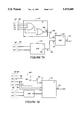
- FIGS. 7A and 7B are illustrations of alternate forms of the gate network in FIG. 4 following a collapse operation 115.
- FIG. 1 shows a block diagram of an EDA system 100 for the computer-assisted electronic engineering and design of prototype circuits and systems.
- the EDA system 100 includes software-implemented circuit design tools in a conventional stand-alone or networked engineering workstation having a micro-processor 101 and a digital storage unit 103.
- the EDA system 100 serves as a platform for electronic circuit prototype definition using a logic synthesis tool 109, and for verification by a logic simulator 141, in conjunction with system or circuit manufacturing using circuit lay-out compaction and routing 139, and mask work creation for circuit fabrication 143.
- the logic synthesis tool 109 is provided as a software program in the storage unit 103 for execution by the processor 101.
- the logic synthesis tool 109 receives a conventional, high-level hardware description file (e.g., Verilog, VHDL, or other similar format) that defines a behavioral model or a register transfer level description of the operations of a prototype circuit or system.
- a logic synthesizer 111 converts the hardware description file into a gate level netlist using conventional means, and then optimizes the netlist in two stages: technology-independent stage 113 and technology-dependent stage 121, prior to outputting an optimized netlist useful for conventional logic simulation 141 or lay-out compaction and routing 139.
- the technology independent stage 113 optimizes the netlist using various modules, including collapse 115, minimize 117 and factor/decompose 119. These modules manipulate the netlist to output an optimized logic description of the prototype circuit to the technology dependent stage 121. The optimized netlist then is decomposed 123 into canonical form and mapped 125 using logic cells from the target library 129.
- the target library 129 includes a plurality of logic cells, along with related geometrical and connectivity information for mapping 125 the decomposed 123 logic expression of the prototype circuit into a specific fabrication technology.
- the target library 129 includes for each logic cell an intrinsic boolean delay value 133.
- the intrinsic boolean delay values 133 represent the delay incurred in generating an output signal from a logic cell for a set of input signals.
- an average resistance-capacitive (R-C) delay value 131 for fan-outs from logic cells in the target library 129.
- the R-C delay value 131 is the product of the average resistance and average capacitance values of selected logic cells in the target library 129.
- the selected logic cells can include all logic cells in the library, or only particular logic cells that will be used for implementing the prototype circuit, thereby increasing the accuracy of the average R-C delay value 131 when it is known which logic cells will be used during mapping 125.
- the R-C delay value 131 and the intrinsic boolean delay values 133 are determined during compilation of the target library 129, thereby avoiding any runtime delay during the technology independent and dependent optimization stages 113, 121.
- the netlist of the prototype circuit output by the logic synthesizer 111 is optimized by logic synthesis tool 109 at technology-independent stage 113 using a technology independent timing analyzer 135 that employs the delay values 131, 133 during a timing analysis 200 (FIG. 2) of a portion of the prototype circuit.
- This optimization occurs independently of and prior to performing further technology-dependent optimization 121, wherein the technology independent timing analyzer 135 can also be employed.
- each of the TI logic optimization substages of collapse 115, minimize 117, and factor/decompose 119 there are various logically equivalent sets of gate networks that can be output from the substage.
- Each of these alternate gate networks have variant total delay values when mapped 125 with logic cells from the target library 129.
- the logic synthesis tool 109 invokes the timing analyzer 135 to individually evaluate the total delay value of each of the possible gate networks output by a TI substage.
- the logic synthesis tool 109 can then select as the optimized output of the substage the gate network having a minimum delay value using the logic cells of the target library 129.
- the timing analysis 200 provided by the timing analyzer 135 in conjunction with any of the modules of the logic synthesis tool 109 is shown in the flowchart of FIG. 2.
- the timing analyzer 135 first obtains 201 the average R-C delay value 131 and the intrinsic delay value 133 of a selected canonical cell from the target library 129. In the preferred embodiment the intrinsic delay value 133 for a NAND2 logic cell is used.
- the timing analyzer 135 also obtains 203 from the logic synthesis tool 109 a logic description for a gate network of a portion of the prototype circuit to be analyzed during optimization of the circuit by one of the TI stage 113 modules.
- FIG. 4 shows an example gate network 400 of a circuit for analysis by the timing analyzer 135.
- the gate network of FIG. 4 includes four nodes 401, labeled V, X, W, and Y, and a number of input signals 403 to the nodes, labeled A, B, C, D, E, and F.
- Each input signal 403 has an input delay value 407, which determines the arrival time of the input signal 403 into the node 401.
- input signal A has a delay value 407 of 0.1 units, using a timing scale appropriate to the fabrication technology for the circuit, typically nanoseconds.
- a node 401 has a node delay value 409 that is the delay incurred by the node 401 to process all of its input signals 403.
- Each node has an output signal 405, here labeled T1, T2 and T3, which feeds into another node 401 as an input signal.
- the output signal 405 also has a delay value that is the total delay value 411 of the node, and includes the node delay value 409 and a wire delay value based on the number of fan-outs for the output signal 405 to other nodes 401 in later logic stages 415.
- the logic expression for the gate network 400 of FIG. 4 is:
- T2 is:
- T1 is:
- the nodes 401 of the gate network 400 can be organized into logic stages 415 through which the input signals 403 must be processed.
- the gate network 400 of FIG. 4 there are three logic stages, with node V as the only node 401 in the first logic stage 415a, nodes W and X in the second logic stage 415b, and node Y in the final logic stage 415c.
- the timing analyzer 135 sorts 205 the nodes 401 of the logic description according to their logic stage 415, thus preserving the processing order of the input signals 403 during the timing analysis 200.
- the timing analyzer 135 decomposes 207 the node to determine a node delay value 409 for the node to process its input signals 403 and produce an output signal 405.
- the decomposition process 207 is further described below, with respect to FIG. 3.
- the results of the decomposition 207 will be provided in order to show the overall operation of the timing analyzer 135.
- node V is structured as in FIG.
- the node delay value 409 of node V is 4.1, as shown in FIG. 5B. The derivation of this value is described below with respect to FIG. 3.
- the timing analyzer 135 determines the wire delay of the output signal 405 of the node 401 when the output signal 405 is input into further nodes 401.
- the wire delay accounts for any fan-out delay from the output signal 405 being input into multiple nodes 401. This is done by determining 209 the number of fan-outs of the output signal of the node 401, and multiplying 211 this number by the average R-C delay value 131 retrieved 201 from the target library 129.
- the average R-C delay value 131 is representative of the average delay for each fan-out, and thus models the wire delay value from a given output signal 405 to a set of nodes 401.
- the combined wire delay value and the node delay value 409 result in the total delay value 411 for the node 401.
- the wire delay value is equal to 1*0.2, or 0.2.
- the total delay value 411 of node V is then determined 213 as the sum of the node delay value 409 and the wire delay value. In FIG. 4, the total delay value 411 of node V is 4.3 following decomposition 207.
- This process is repeated 215 for each node 401 in each logic stage 415 of the gate network 400, thereby generating a total delay value 411 for each node 401.
- the total delay value 413 of the entire gate network 400 will be the total delay value 411 of output signal of the last node 401 in the gate network. This is because the delay value of each of the input signals for the last node 401 in the last logic stage 415 will be the total delay values 411 of each of nodes 401 in the prior logic stage 415.
- the total delay value 413 of the gate network 400 is 6.7, and represents the minimized delay value 413 for the specific gate network (assuming the minimization 117 described below, without collapsing 115 or factoring/decomposing 119) passed to the timing analyzer 135 by the logic synthesis tool 109.
- the total delay value 413 of the gate network 400 is returned 217 to the logic synthesis tool 109, which can compare it to the total delay values 413 of other logically equivalent, but structurally different gate networks that have been analyzed by the timing analyzer 135 to determine which gate network provides the minimum timing delay.
- the gate network with the minimum total delay value 413 will then be chosen by appropriate module of the logic synthesis tool 109 for optimizing the circuit during that module's processing function.
- FIG. 3 shows the decomposition 207 process used during the timing analysis 200.
- the logic expression of each node is obtained 301 from the logic description of the gate network provided to the timing analyzer 135 by the logic synthesis tool 109.
- the logic expression is preferably in sum of products form. In the sum of products form, there will be two stages of logic, an AND stage including a number of product logic terms, and an OR stage with a single sum logic term. Each of these logic terms is analyzed as follows.
- the delay values 407 of the input signals 403 of the logic term are obtained 303. These delay values will be determined based on either the fixed delay values for the input signals 403 entering the gate network 400, or previously determined by the timing analyzer 135 in analyzing a node 401 in a prior logic stage 415, as the output signals from one node 400 become the input signals to a next node 400.
- the input signals 403 of the logic term form an input list.
- the timing analyzer 135 thus begins the process with node V in the first logic stage 415, and decomposes 207 that node.
- the equation for node V is:
- the gate network for this equation prior to decomposition 207 is shown in FIG. 5A.
- the input signal 403 to each subexpression have the same delay values 407, based on the fan-in delays.
- the delay value after each AND4 in the AND logic stage is 3.3, based on the latest arriving input signal C, with a delay of 1.8, and an intrinsic boolean delay value 133 of 1.5.
- the OR5 has an intrinsic boolean delay value of 2.0, and as all the input signal to the OR5 have a delay of 3.3, the node delay value 409 is 5.3.
- the decomposition 207 of node V is illustrated in FIG. 5B, as follows.
- the first product term of the logic expression of node V, (ABCD) is obtained 301 from the equation for the node and storing the input signals (A, B, C, D) in the input list.
- the input list is sorted 305 by the delay value 407 of each input signal 403, which already includes the fan-in delay, if any, of each input signal.
- the fan-in delay is the average R-C delay 131 from the target library, times the number of terms that include the input signal as a literal.
- input signal A is input into five terms, so its fan-in delay is 1.0, assuming a 0.2 R-C delay 131.
- the input delay value 407 for input signal A is then 1.1, since input signal A has an initial delay value of 0.1.
- the input delay 501 for signals B, C, and D is 1.0, 1.8, and 1.2, respectively, each having a fan-in delay of 1.0. Sorting the input signals 403 by their input delays 407, results in an ordered list of input signals from least to greatest delay value, here (B, A, D, C).
- a first set of input signals 403 is selected 307 from the input list.
- the first set of input signals 403 are those signals with the lowest input delay values 407, and thus represent the earliest arriving input signals 403 for the product term.
- two input signals are selected, which in this example is input signals (B, A).
- the timing analyzer 135 determines 311 an output delay value for an intermediate output signal T4 for the input signals.
- the output delay value 503 is computed from largest delay value of the selected input signals 403.
- the output delay value 503 will be the delay value of the last input signal in the selected group plus the intrinsic delay value 133 of a canonical logic cell from the target library 129 for processing the input signals 403.
- the intrinsic delay value 133 of a NAND2 cell is used.
- the intrinsic delay value 133 of the NAND2 from the target library 129 closely models the actual timing delay value that would result from mapping the gate network 400 using the target library. It thus allows the logic synthesis tool 109 to select the gate network having the minimized delay given the target library 129.
- FIG. 5B illustrates the determination of the output delays 503, showing that the intermediate output signal T4 for input signals A and B has a delay 503 of 1.6since the intrinsic delay value 133 of the NAND2 is assumed here to be 0.5, and the largest input delay value 501 is 1.1 from input signal A.
- the use of the NAND2 gate in FIG. 5B is for illustration of the operation of the decomposition 207 process only, and does not represent that input signals 403 have been actually mapped to a NAND2 logic cell.
- a larger number of input signals such as three input signals could be selected, and the intrinsic delay value 133 of a NAND3 would be used 311 to determine the output delay value.
- the intrinsic delay values 133 of NOR logic cells in the target library 129 with the appropriate input signals could be used 311.
- timing analyzer 135 is invoked by the canonical decomposition module 123, an extra step is performed whereby a NAND2 logic cell (or other appropriate logic cell depending on the number of selected input signals 403 for that embodiment) is assigned 309 to the selected input signals 403, and provided in a netlist of the gate network.
- the input signals (B, A) are removed 313 from the input list and the intermediate output signal T4 is added to the input list, resulting in (D, C, T4).
- the intermediate output signal is added to the input list because it now will be an input signal to another logic term in the node, and its delay value 503 determines the input delay for that logic term.
- the ordered input list following the first pass through sequence 305-315 is (D, C, T4), and thus loop 321 is repeated.
- the list is sorted 305 the order becomes (D, T4, C) since the delay value 503 of T4 is less than the delay value 407 of C.
- a set of input signals is selected 307, here (D, T4), and the output delay 503 for another intermediate output signal T5 is computed 311, as equal to 2.1, since now T4 is the later arriving signal with a delay of 1.6, plus the intrinsic delay value 133 of 0.5.
- the input signals are again removed 313 from the input list, and the intermediate output signal T5 is added to the input list, as before. In this case, this leaves the input list as (C, T5).
- the loop 321 is repeated as long as there is more than one input left in the input list, and results in a timing analysis of the supplied logic term.
- the input list now contains two input signals, (C, T5) so loop 321 is again repeated.
- the input list is sorted 305, leaving it in is current order, and the input signals selected 307.
- the output delay 503 for another intermediate output signal T6 is determined 311, here equal to 2.6, using the delay of T5 and the intrinsic delay value 133 of the NAND2.
- the output signal T6a is placed in the input list, and the input signals (C, T5) are removed, leaving only signal T6a. Since the input list contains only one term, loop 321 is not repeated, and the output signal T6a of the product logic term is stored as an input signal for a sum logic term in the OR stage.
- a second conditional 317 tests whether there are any further logic terms in the logic expression of node V. If so, the next logic term, here (ABCD), is obtained 301, and the above decomposition analysis repeated in loop 323.
- the input signals (A, B, C, D) are obtained 303, and sorted 305 to provide an input list of (B, A, D, C).
- the input delays for all of the input signals for this product logic terms are the same as before, and are the same for all the terms.
- the decomposition of each of the remaining logic terms is the same as the decomposition of the first term, and is illustrated in FIG. 5B by the repetition of the cascaded NAND logic cells 505.
- each product logic term in Eq. 3 has output delay of 2.6 for an intermediate output signal T6(a-e) that is used as an input to the OR stage.
- the input signals to the OR stage are (T6a, T6b, T6c, T6d, T6d, T6e ) and for the input list.
- the list is sorted 305, but since all the delay values are the same, there is no change in order.
- (T6a, T6b ) are used as input signals for determining 311 an output delay value 503 of 3.1 for an intermediate output signal T7.
- Intermediate output signals T6a and T6b are removed 313 from the input list, and T10 is added to the list.
- the input list now contains (T8, T9) so the loop 321 is repeated for the last time, to produce the output signal T1 for the node with a node output delay 409 of 4.1.
- This delay value more accurately reflects the delay of the node that would follow canonical decomposition 123 and mapping 125 than delay value of 5.3 derived from the unanalyzed node.
- the timing analyzer 135 can be invoked by any of the T1 stage modules to determine the timing delay value for various alternate gate networks resulting from the modules operation.
- the timing analyzer 135 can be used by the minimize 117 module to determine the optimal minimized form of node V.
- a Karnaugh map of Eq. 3 for node V shows two possible simplifications: ##STR1##
- Each equation for the simplified node is sent separately to the timing analyzer 135 to determine which simplified logic expression results in the minimized timing delay, and hence is the optimal implementation for node V using the logic cells of the target library 129.
- the results of the timing analysis 200 on each logic expression are shown in FIGS. 6A and 6B. Shown in each figure are input signals A, B, C, and D, and their various delay values 501, 503 occurring for each input and output signal in each logic stage.
- the equations used here are for simple illustration of the timing analysis method, and those of ordinary skill in the art will recognize that the method can be applied to equations having numerous terms and literals.
- the timing analyzer 135 when it receives the logic expression for node V, it performs the decomposition 207 described above, ordering the input signals, determining the delay for each intermediate output signal of a NAND2, and so, to produce a node output delay value for each of the alternate simplified nodes of Eqs. 5 and 6.
- the output signal T11 for the node has output delay value of 2.8, which is the node delay value 409 for the simplified node.
- the node delay value is 2.9 at output signal T11', as shown in FIG. 6B. This delay value is greater than the previous delay value at T11 because of the additional fan-in delay of input signal C, which is a literal in all three product terms of Eq. 6, where it was only in two product terms of Eq. 4.
- the logic synthesis tool 109 would thus select Eq. 5 as the optimized simplified form for node V.
- timing analysis 200 of the timing analyzer 135 has been shown with the minimize 117 module of logic synthesis tool 109.
- the timing analysis 200 can also be used with the other modules.
- the circuit of FIG. 4 could be collapsed 115 in a variety of different ways, with nodes V and W being collapsed to W', or nodes W and Y being collapsed in Y', or nodes X and Y being collapsed into Y'.
- the logic synthesis tool 109 would send a logic expression for each collapsed version to the timing analyzer 135, which would determine the total node value 409 for each version.
- FIG. 7A shows the results of the first option, where:
- the timing analyzer 135 determines that T2' equals 1.8 for W' structured according to Eq. 9. This would reduce the total delay value 413' for the gate network of FIG. 4A to 3.2 from its original value of 6.7. In comparison, collapsing W and Y into Y', as illustrated in FIG. 7B, results in the following expression:
- the timing analysis 200 of the timing analyzer 135 can also be used during the technology dependent optimization stage 121.
- a canonical decomposition module 123 decomposes a boolean expression for the gate network output from the TI stage 113 into canonical form using only canonical logic cells, such as NAND2 and Invertor.
- the timing analyzer 135 employs an additional step to assign 309 the input signals 403 to a NAND2 logic cell from the target library 129, create a NAND2 logic cell, and place it into the decomposed circuit.
- the decomposed gate network is then mapped 125 with the logic cells from the target library 129 by the map module 125, which conventionally selects an arrangement of logic cells for implementing the prototype circuit.
Abstract
Description
OUT=T2T3+T2T3 Eq. 1
(A)(T1)+C Eq. 2
ABCD+ABCD+ABCD+ABCD+ABCD Eq. 3
EF+EF Eq. 4
T1=AB CD+AB CD+ABCD+ABCD+ABC D Eq. 3
T2=A(T1)+C Eq. 7
T2=A(ABCD+ABCD+ABCD+ABCD+ABCD)+C Eq. 8
T2=ABD+C Eq. 9
OUT=T2T3+T2T3 Eq. 10
T2=A(T1)+C,
OUT=(AT1+C)T3+(AT1+C)T3 Eq. 11
OUT=AT1T3+CT3+A C T3+T1 C T3 Eq. 12
Claims (10)
Priority Applications (1)
| Application Number | Priority Date | Filing Date | Title |
|---|---|---|---|
| US08/249,868 US5475605A (en) | 1994-05-26 | 1994-05-26 | Timing analysis for logic optimization using target library delay values |
Applications Claiming Priority (1)
| Application Number | Priority Date | Filing Date | Title |
|---|---|---|---|
| US08/249,868 US5475605A (en) | 1994-05-26 | 1994-05-26 | Timing analysis for logic optimization using target library delay values |
Publications (1)
| Publication Number | Publication Date |
|---|---|
| US5475605A true US5475605A (en) | 1995-12-12 |
Family
ID=22945347
Family Applications (1)
| Application Number | Title | Priority Date | Filing Date |
|---|---|---|---|
| US08/249,868 Expired - Lifetime US5475605A (en) | 1994-05-26 | 1994-05-26 | Timing analysis for logic optimization using target library delay values |
Country Status (1)
| Country | Link |
|---|---|
| US (1) | US5475605A (en) |
Cited By (56)
| Publication number | Priority date | Publication date | Assignee | Title |
|---|---|---|---|---|
| US5636130A (en) * | 1995-07-05 | 1997-06-03 | Sun Microsystems, Inc. | Method of determining signal propagation delay through circuit elements |
| US5644498A (en) * | 1995-01-25 | 1997-07-01 | Lsi Logic Corporation | Timing shell generation through netlist reduction |
| US5687088A (en) * | 1993-05-19 | 1997-11-11 | Matsushita Electric Industrial Co., Ltd. | Net list for use in logic simulation and back annotation method of feedbacking delay information obtained through layout design to logic simulation |
| US5715170A (en) * | 1994-04-20 | 1998-02-03 | Fujitsu Limited | Apparatus for forming input data for a logic simulator |
| US5724557A (en) * | 1995-07-10 | 1998-03-03 | Motorola, Inc. | Method for designing a signal distribution network |
| US5726918A (en) * | 1995-06-05 | 1998-03-10 | Synopsys, Inc. | Tool, system and method for dynamic timing analysis in a plural-instance digital system simulation |
| US5745373A (en) * | 1994-03-11 | 1998-04-28 | Hitachi, Ltd. | Logic circuit generating method and apparatus |
| US5751593A (en) * | 1996-04-10 | 1998-05-12 | Motorola, Inc. | Accurate delay prediction based on multi-model analysis |
| US5796993A (en) * | 1996-10-29 | 1998-08-18 | Maguire; Jeffrey E. | Method and apparatus for semiconductor device optimization using on-chip verification |
| US5815405A (en) * | 1996-03-12 | 1998-09-29 | Xilinx, Inc. | Method and apparatus for converting a programmable logic device representation of a circuit into a second representation of the circuit |
| US5838580A (en) * | 1996-06-20 | 1998-11-17 | Sun Microsystems, Inc. | Method of optimizing repeater placement in long lines of a complex integrated circuit |
| US5844818A (en) * | 1996-05-10 | 1998-12-01 | Lsi Logic Corporation | Method for creating and using design shells for integrated circuit designs |
| US5883809A (en) * | 1996-07-26 | 1999-03-16 | 3 Com Corporation | Behavioral language models for testing and verification of digital electronic circuits |
| US5886900A (en) * | 1996-09-25 | 1999-03-23 | Lsi Logic Gorporation | Protection of proprietary circuit designs during gate level static timing analysis |
| US5896300A (en) * | 1996-08-30 | 1999-04-20 | Avant| Corporation | Methods, apparatus and computer program products for performing post-layout verification of microelectronic circuits by filtering timing error bounds for layout critical nets |
| US5946475A (en) * | 1997-01-21 | 1999-08-31 | International Business Machines Corporation | Method for performing transistor-level static timing analysis of a logic circuit |
| US5949983A (en) * | 1996-04-18 | 1999-09-07 | Xilinx, Inc. | Method to back annotate programmable logic device design files based on timing information of a target technology |
| US5949993A (en) * | 1997-10-31 | 1999-09-07 | Production Languages Corporation | Method for the generation of ISA simulators and assemblers from a machine description |
| US5978572A (en) * | 1996-08-21 | 1999-11-02 | Matsushita Electric Industrial Co., Ltd. | LSI wire length estimation and area estimation |
| US6009253A (en) * | 1996-06-20 | 1999-12-28 | Sun Microsystems, Inc. | Spare repeater amplifiers for long lines on complex integrated circuits |
| US6009252A (en) * | 1998-03-05 | 1999-12-28 | Avant! Corporation | Methods, apparatus and computer program products for determining equivalencies between integrated circuit schematics and layouts using color symmetrizing matrices |
| US6014510A (en) * | 1996-11-27 | 2000-01-11 | International Business Machines Corporation | Method for performing timing analysis of a clock circuit |
| US6052524A (en) * | 1998-05-14 | 2000-04-18 | Software Development Systems, Inc. | System and method for simulation of integrated hardware and software components |
| US6185723B1 (en) | 1996-11-27 | 2001-02-06 | International Business Machines Corporation | Method for performing timing analysis of a clock-shaping circuit |
| US6219819B1 (en) | 1998-06-26 | 2001-04-17 | Xilinx, Inc. | Method for verifying timing in a hard-wired IC device modeled from an FPGA |
| US6243852B1 (en) * | 1997-08-29 | 2001-06-05 | Nec Corporation | Method of and an apparatus for logic circuit synthesis |
| US6249147B1 (en) | 1999-03-09 | 2001-06-19 | Fujitsu, Ltd. | Method and apparatus for high speed on-chip signal propagation |
| US6272668B1 (en) | 1994-12-14 | 2001-08-07 | Hyundai Electronics America, Inc. | Method for cell swapping to improve pre-layout to post-layout timing |
| KR100335376B1 (en) * | 1999-11-19 | 2002-05-06 | 조양호 | Resynthesis system and the method for time delay constraint of digital circuits |
| US6453446B1 (en) | 1997-12-24 | 2002-09-17 | Magma Design Automation, Inc. | Timing closure methodology |
| US6457159B1 (en) * | 1998-12-29 | 2002-09-24 | Cadence Design Systems, Inc. | Functional timing analysis for characterization of virtual component blocks |
| US20020156610A1 (en) * | 1997-03-04 | 2002-10-24 | Mitsubishi Denki Kabushiki Kaisha | Gate delay calculation apparatus and method thereof using parameter expressing RC model source resistance value |
| US6518801B1 (en) * | 1999-08-05 | 2003-02-11 | Agere Systems Inc. | Alias suppression method for 1-bit precision direct digital synthesizer |
| US20030046640A1 (en) * | 2001-08-29 | 2003-03-06 | Wheeler William R. | Generating a logic design |
| US20030046652A1 (en) * | 2001-08-29 | 2003-03-06 | Wheeler William R. | Gate estimation process and method |
| US6543037B1 (en) * | 1997-03-14 | 2003-04-01 | Cadence Design Systems, Inc. | Delay estimation for restructuring the technology independent circuit |
| US6601220B1 (en) * | 1996-10-22 | 2003-07-29 | International Business Machines Corporation | Method for transistor-level calculation of the precharge time of domino logic circuits with unlocked evaluation paths |
| US6629298B1 (en) * | 1999-11-10 | 2003-09-30 | International Business Machines Corporation | Automated programmable process and method for the improvement of electrical digital signal transition rates in a VLSI design |
| US6721925B2 (en) * | 2001-08-29 | 2004-04-13 | Intel Corporation | Employing intelligent logical models to enable concise logic representations for clarity of design description and for rapid design capture |
| US20040073877A1 (en) * | 2002-04-16 | 2004-04-15 | Jones Anthony Mark | Method of determining library parameters using timing surface planarity |
| US6760894B1 (en) * | 1999-12-28 | 2004-07-06 | Cadence Design Systems, Inc. | Method and mechanism for performing improved timing analysis on virtual component blocks |
| US6859913B2 (en) | 2001-08-29 | 2005-02-22 | Intel Corporation | Representing a simulation model using a hardware configuration database |
| US20050283744A1 (en) * | 2004-06-18 | 2005-12-22 | Fujitsu Limited | Integrated circuit designing system, method and program |
| US20060123378A1 (en) * | 2004-12-03 | 2006-06-08 | Ipextreme Inc. | Method, System, and Software Product For Using Synthesizable Semiconductor Intellectual Property In Self-Documenting Electronic Extended Package |
| US7082104B2 (en) | 2001-05-18 | 2006-07-25 | Intel Corporation | Network device switch |
| US7093224B2 (en) | 2001-08-28 | 2006-08-15 | Intel Corporation | Model-based logic design |
| US7107201B2 (en) | 2001-08-29 | 2006-09-12 | Intel Corporation | Simulating a logic design |
| US7130784B2 (en) | 2001-08-29 | 2006-10-31 | Intel Corporation | Logic simulation |
| US7197724B2 (en) | 2002-01-17 | 2007-03-27 | Intel Corporation | Modeling a logic design |
| US20070113211A1 (en) * | 2005-11-17 | 2007-05-17 | Lizheng Zhang | Efficient statistical timing analysis of circuits |
| US20090070720A1 (en) * | 2007-09-11 | 2009-03-12 | International Business Machines Corporation | System to Identify Timing Differences from Logic Block Changes and Associated Methods |
| US20090070719A1 (en) * | 2007-09-11 | 2009-03-12 | International Business Machines Corporation | Logic Block Timing Estimation Using Conesize |
| US7617470B1 (en) * | 2005-10-11 | 2009-11-10 | California Institute Of Technology | Reconfigurable integrated circuit and method for increasing performance of a reconfigurable integrated circuit |
| US7739324B1 (en) * | 2006-03-22 | 2010-06-15 | Cadence Design Systems, Inc. | Timing driven synthesis of sum-of-product functional blocks |
| US8453090B2 (en) | 2010-10-21 | 2013-05-28 | Global Unichip Corp. | System and method for optimizing logic timing |
| US9519746B1 (en) | 2015-06-11 | 2016-12-13 | International Business Machines Corporation | Addressing early mode slack fails by book decomposition |
Citations (11)
| Publication number | Priority date | Publication date | Assignee | Title |
|---|---|---|---|---|
| US5168455A (en) * | 1991-03-28 | 1992-12-01 | Digital Equipment Corporation | Procedure for incorporating timing parameters in the synthesis of logic circuit designs |
| US5210700A (en) * | 1990-02-20 | 1993-05-11 | International Business Machines Corporation | Automatic delay adjustment for static timing analysis |
| US5287289A (en) * | 1990-04-13 | 1994-02-15 | Hitachi, Ltd. | Logic synthesis method |
| US5293327A (en) * | 1990-06-25 | 1994-03-08 | Mitsubishi Denki Kabushiki Kaisha | Method of logic circuit simulation |
| US5305229A (en) * | 1991-09-06 | 1994-04-19 | Bell Communications Research, Inc. | Switch-level timing simulation based on two-connected components |
| US5333032A (en) * | 1990-08-20 | 1994-07-26 | Matsushita Electric Industrial Co., Ltd. | Logic design system and method in the same |
| US5353433A (en) * | 1990-09-06 | 1994-10-04 | Digital Equipment Corporation | Method and apparatus for organizing and analyzing timing information |
| US5359535A (en) * | 1992-05-04 | 1994-10-25 | Motorola, Inc. | Method for optimization of digital circuit delays |
| US5365463A (en) * | 1990-12-21 | 1994-11-15 | International Business Machines Corporation | Method for evaluating the timing of digital machines with statistical variability in their delays |
| US5381345A (en) * | 1991-09-02 | 1995-01-10 | Rohm Co., Ltd. | Logic-circuit layout pattern inspection method and logical simulation |
| US5384720A (en) * | 1993-06-10 | 1995-01-24 | Hitachi Micro Systems Inc. | Logic circuit simulator and logic simulation method having reduced number of simulation events |
-
1994
- 1994-05-26 US US08/249,868 patent/US5475605A/en not_active Expired - Lifetime
Patent Citations (11)
| Publication number | Priority date | Publication date | Assignee | Title |
|---|---|---|---|---|
| US5210700A (en) * | 1990-02-20 | 1993-05-11 | International Business Machines Corporation | Automatic delay adjustment for static timing analysis |
| US5287289A (en) * | 1990-04-13 | 1994-02-15 | Hitachi, Ltd. | Logic synthesis method |
| US5293327A (en) * | 1990-06-25 | 1994-03-08 | Mitsubishi Denki Kabushiki Kaisha | Method of logic circuit simulation |
| US5333032A (en) * | 1990-08-20 | 1994-07-26 | Matsushita Electric Industrial Co., Ltd. | Logic design system and method in the same |
| US5353433A (en) * | 1990-09-06 | 1994-10-04 | Digital Equipment Corporation | Method and apparatus for organizing and analyzing timing information |
| US5365463A (en) * | 1990-12-21 | 1994-11-15 | International Business Machines Corporation | Method for evaluating the timing of digital machines with statistical variability in their delays |
| US5168455A (en) * | 1991-03-28 | 1992-12-01 | Digital Equipment Corporation | Procedure for incorporating timing parameters in the synthesis of logic circuit designs |
| US5381345A (en) * | 1991-09-02 | 1995-01-10 | Rohm Co., Ltd. | Logic-circuit layout pattern inspection method and logical simulation |
| US5305229A (en) * | 1991-09-06 | 1994-04-19 | Bell Communications Research, Inc. | Switch-level timing simulation based on two-connected components |
| US5359535A (en) * | 1992-05-04 | 1994-10-25 | Motorola, Inc. | Method for optimization of digital circuit delays |
| US5384720A (en) * | 1993-06-10 | 1995-01-24 | Hitachi Micro Systems Inc. | Logic circuit simulator and logic simulation method having reduced number of simulation events |
Non-Patent Citations (12)
| Title |
|---|
| Berman, C. L. et al., "Efficient Techniques for Timing Correction" IEEE, 415-419, 1990. |
| Berman, C. L. et al., Efficient Techniques for Timing Correction IEEE, 415 419, 1990. * |
| Burnstein, M. and Youssef, M., "Timing Influenced Layout Design" IEEE, 22nd Design Automation Conference; Paper 9.2, 124-130, 1985. |
| Burnstein, M. and Youssef, M., Timing Influenced Layout Design IEEE, 22nd Design Automation Conference; Paper 9.2, 124 130, 1985. * |
| Chen, K. C. and Muroga, Saburo, "Timing Optimization for Multi-Level Combinational Networks" IEEE, 27th ACM/IEEE Design Automation Conference, Paper 21.1, 339-344, 1990. |
| Chen, K. C. and Muroga, Saburo, Timing Optimization for Multi Level Combinational Networks IEEE, 27th ACM/IEEE Design Automation Conference, Paper 21.1, 339 344, 1990. * |
| Dunlop, A. E et al., "Chip Layout Optimization Using Critical Path Weighting" IEEE, 21st Design Automation Conference, Paper 9.2 133-136, 1984. |
| Dunlop, A. E et al., Chip Layout Optimization Using Critical Path Weighting IEEE, 21st Design Automation Conference, Paper 9.2 133 136, 1984. * |
| Singh, K. J. et al., "Timing Optimization of Combinational Logic" IEEE, 282-285, 1988. |
| Singh, K. J. et al., Timing Optimization of Combinational Logic IEEE, 282 285, 1988. * |
| Teig, S. et al., "Timing-Driven Layout of Cell-Based ICs" VLSI Systems Design, 63-73, May 1986. |
| Teig, S. et al., Timing Driven Layout of Cell Based ICs VLSI Systems Design, 63 73, May 1986. * |
Cited By (74)
| Publication number | Priority date | Publication date | Assignee | Title |
|---|---|---|---|---|
| US5687088A (en) * | 1993-05-19 | 1997-11-11 | Matsushita Electric Industrial Co., Ltd. | Net list for use in logic simulation and back annotation method of feedbacking delay information obtained through layout design to logic simulation |
| US5745373A (en) * | 1994-03-11 | 1998-04-28 | Hitachi, Ltd. | Logic circuit generating method and apparatus |
| US5715170A (en) * | 1994-04-20 | 1998-02-03 | Fujitsu Limited | Apparatus for forming input data for a logic simulator |
| US6272668B1 (en) | 1994-12-14 | 2001-08-07 | Hyundai Electronics America, Inc. | Method for cell swapping to improve pre-layout to post-layout timing |
| US5644498A (en) * | 1995-01-25 | 1997-07-01 | Lsi Logic Corporation | Timing shell generation through netlist reduction |
| US5726918A (en) * | 1995-06-05 | 1998-03-10 | Synopsys, Inc. | Tool, system and method for dynamic timing analysis in a plural-instance digital system simulation |
| US5636130A (en) * | 1995-07-05 | 1997-06-03 | Sun Microsystems, Inc. | Method of determining signal propagation delay through circuit elements |
| US5724557A (en) * | 1995-07-10 | 1998-03-03 | Motorola, Inc. | Method for designing a signal distribution network |
| US5815405A (en) * | 1996-03-12 | 1998-09-29 | Xilinx, Inc. | Method and apparatus for converting a programmable logic device representation of a circuit into a second representation of the circuit |
| US5751593A (en) * | 1996-04-10 | 1998-05-12 | Motorola, Inc. | Accurate delay prediction based on multi-model analysis |
| US6018624A (en) * | 1996-04-18 | 2000-01-25 | Xilinx, Inc. | Method to back annotate programmable logic device design files based on timing information of a target technology |
| US5949983A (en) * | 1996-04-18 | 1999-09-07 | Xilinx, Inc. | Method to back annotate programmable logic device design files based on timing information of a target technology |
| US5844818A (en) * | 1996-05-10 | 1998-12-01 | Lsi Logic Corporation | Method for creating and using design shells for integrated circuit designs |
| US5838580A (en) * | 1996-06-20 | 1998-11-17 | Sun Microsystems, Inc. | Method of optimizing repeater placement in long lines of a complex integrated circuit |
| US6009253A (en) * | 1996-06-20 | 1999-12-28 | Sun Microsystems, Inc. | Spare repeater amplifiers for long lines on complex integrated circuits |
| US5883809A (en) * | 1996-07-26 | 1999-03-16 | 3 Com Corporation | Behavioral language models for testing and verification of digital electronic circuits |
| US5978572A (en) * | 1996-08-21 | 1999-11-02 | Matsushita Electric Industrial Co., Ltd. | LSI wire length estimation and area estimation |
| US5896300A (en) * | 1996-08-30 | 1999-04-20 | Avant| Corporation | Methods, apparatus and computer program products for performing post-layout verification of microelectronic circuits by filtering timing error bounds for layout critical nets |
| US6286126B1 (en) | 1996-08-30 | 2001-09-04 | Avant! Corporation | Methods, apparatus and computer program products for performing post-layout verification of microelectronic circuits using best and worst case delay models for nets therein |
| US5886900A (en) * | 1996-09-25 | 1999-03-23 | Lsi Logic Gorporation | Protection of proprietary circuit designs during gate level static timing analysis |
| US6601220B1 (en) * | 1996-10-22 | 2003-07-29 | International Business Machines Corporation | Method for transistor-level calculation of the precharge time of domino logic circuits with unlocked evaluation paths |
| US5796993A (en) * | 1996-10-29 | 1998-08-18 | Maguire; Jeffrey E. | Method and apparatus for semiconductor device optimization using on-chip verification |
| US6185723B1 (en) | 1996-11-27 | 2001-02-06 | International Business Machines Corporation | Method for performing timing analysis of a clock-shaping circuit |
| US6014510A (en) * | 1996-11-27 | 2000-01-11 | International Business Machines Corporation | Method for performing timing analysis of a clock circuit |
| US5946475A (en) * | 1997-01-21 | 1999-08-31 | International Business Machines Corporation | Method for performing transistor-level static timing analysis of a logic circuit |
| US20020156610A1 (en) * | 1997-03-04 | 2002-10-24 | Mitsubishi Denki Kabushiki Kaisha | Gate delay calculation apparatus and method thereof using parameter expressing RC model source resistance value |
| US6510404B1 (en) | 1997-03-04 | 2003-01-21 | Mitsubishi Denki Kabushiki Kaisha | Gate delay calculation apparatus and method thereof using parameter expressing RC model source resistance value |
| US6543037B1 (en) * | 1997-03-14 | 2003-04-01 | Cadence Design Systems, Inc. | Delay estimation for restructuring the technology independent circuit |
| US6243852B1 (en) * | 1997-08-29 | 2001-06-05 | Nec Corporation | Method of and an apparatus for logic circuit synthesis |
| US5949993A (en) * | 1997-10-31 | 1999-09-07 | Production Languages Corporation | Method for the generation of ISA simulators and assemblers from a machine description |
| US6453446B1 (en) | 1997-12-24 | 2002-09-17 | Magma Design Automation, Inc. | Timing closure methodology |
| US8621403B2 (en) | 1997-12-24 | 2013-12-31 | Synopsys, Inc. | Timing closure methodology including placement with initial delay values |
| US6725438B2 (en) | 1997-12-24 | 2004-04-20 | Magma Design Automation, Inc. | Timing closure methodology |
| US20050120319A1 (en) * | 1997-12-24 | 2005-06-02 | Van Ginneken Lukas P. | Timing closure methodology |
| US9811624B2 (en) | 1997-12-24 | 2017-11-07 | Synopsys, Inc. | Timing closure methodology including placement with initial delay values |
| US6009252A (en) * | 1998-03-05 | 1999-12-28 | Avant! Corporation | Methods, apparatus and computer program products for determining equivalencies between integrated circuit schematics and layouts using color symmetrizing matrices |
| US6052524A (en) * | 1998-05-14 | 2000-04-18 | Software Development Systems, Inc. | System and method for simulation of integrated hardware and software components |
| US6625788B1 (en) | 1998-06-26 | 2003-09-23 | Xilinx, Inc. | Method for verifying timing in a hard-wired IC device modeled from an FPGA |
| US6219819B1 (en) | 1998-06-26 | 2001-04-17 | Xilinx, Inc. | Method for verifying timing in a hard-wired IC device modeled from an FPGA |
| US20030140324A1 (en) * | 1998-12-29 | 2003-07-24 | Hakan Yalcin | Functional timing analysis for characterization of virtual component blocks |
| US6457159B1 (en) * | 1998-12-29 | 2002-09-24 | Cadence Design Systems, Inc. | Functional timing analysis for characterization of virtual component blocks |
| US7346872B2 (en) | 1998-12-29 | 2008-03-18 | Cadence Design Systems, Inc. | Functional timing analysis for characterization of virtual component blocks |
| US6249147B1 (en) | 1999-03-09 | 2001-06-19 | Fujitsu, Ltd. | Method and apparatus for high speed on-chip signal propagation |
| US6518801B1 (en) * | 1999-08-05 | 2003-02-11 | Agere Systems Inc. | Alias suppression method for 1-bit precision direct digital synthesizer |
| US6629298B1 (en) * | 1999-11-10 | 2003-09-30 | International Business Machines Corporation | Automated programmable process and method for the improvement of electrical digital signal transition rates in a VLSI design |
| KR100335376B1 (en) * | 1999-11-19 | 2002-05-06 | 조양호 | Resynthesis system and the method for time delay constraint of digital circuits |
| US6760894B1 (en) * | 1999-12-28 | 2004-07-06 | Cadence Design Systems, Inc. | Method and mechanism for performing improved timing analysis on virtual component blocks |
| US7082104B2 (en) | 2001-05-18 | 2006-07-25 | Intel Corporation | Network device switch |
| US7093224B2 (en) | 2001-08-28 | 2006-08-15 | Intel Corporation | Model-based logic design |
| US6859913B2 (en) | 2001-08-29 | 2005-02-22 | Intel Corporation | Representing a simulation model using a hardware configuration database |
| US20030046640A1 (en) * | 2001-08-29 | 2003-03-06 | Wheeler William R. | Generating a logic design |
| US6983427B2 (en) | 2001-08-29 | 2006-01-03 | Intel Corporation | Generating a logic design |
| US20030046652A1 (en) * | 2001-08-29 | 2003-03-06 | Wheeler William R. | Gate estimation process and method |
| US7073156B2 (en) | 2001-08-29 | 2006-07-04 | Intel Corporation | Gate estimation process and method |
| US7107201B2 (en) | 2001-08-29 | 2006-09-12 | Intel Corporation | Simulating a logic design |
| US7130784B2 (en) | 2001-08-29 | 2006-10-31 | Intel Corporation | Logic simulation |
| US6721925B2 (en) * | 2001-08-29 | 2004-04-13 | Intel Corporation | Employing intelligent logical models to enable concise logic representations for clarity of design description and for rapid design capture |
| US7197724B2 (en) | 2002-01-17 | 2007-03-27 | Intel Corporation | Modeling a logic design |
| US6813753B2 (en) | 2002-04-16 | 2004-11-02 | Micron Technology, Inc. | Method of determining library parameters using timing surface planarity |
| US20040073877A1 (en) * | 2002-04-16 | 2004-04-15 | Jones Anthony Mark | Method of determining library parameters using timing surface planarity |
| US7111261B2 (en) | 2002-04-16 | 2006-09-19 | Micron Technology, Inc. | Method of determining library parameters using timing surface planarity |
| US7260791B2 (en) * | 2004-06-18 | 2007-08-21 | Fujitsu Limited | Integrated circuit designing system, method and program |
| US20050283744A1 (en) * | 2004-06-18 | 2005-12-22 | Fujitsu Limited | Integrated circuit designing system, method and program |
| US20060123378A1 (en) * | 2004-12-03 | 2006-06-08 | Ipextreme Inc. | Method, System, and Software Product For Using Synthesizable Semiconductor Intellectual Property In Self-Documenting Electronic Extended Package |
| US7617470B1 (en) * | 2005-10-11 | 2009-11-10 | California Institute Of Technology | Reconfigurable integrated circuit and method for increasing performance of a reconfigurable integrated circuit |
| US20090278564A1 (en) * | 2005-10-11 | 2009-11-12 | Dehon Andre M | Reconfigurable integrated circuit and method for increasing performance of a reconfigurable integrated circuit |
| US20070113211A1 (en) * | 2005-11-17 | 2007-05-17 | Lizheng Zhang | Efficient statistical timing analysis of circuits |
| US7350171B2 (en) | 2005-11-17 | 2008-03-25 | Lizheng Zhang | Efficient statistical timing analysis of circuits |
| US7739324B1 (en) * | 2006-03-22 | 2010-06-15 | Cadence Design Systems, Inc. | Timing driven synthesis of sum-of-product functional blocks |
| US20090070720A1 (en) * | 2007-09-11 | 2009-03-12 | International Business Machines Corporation | System to Identify Timing Differences from Logic Block Changes and Associated Methods |
| US20090070719A1 (en) * | 2007-09-11 | 2009-03-12 | International Business Machines Corporation | Logic Block Timing Estimation Using Conesize |
| US7676779B2 (en) | 2007-09-11 | 2010-03-09 | International Business Machines Corporation | Logic block timing estimation using conesize |
| US8453090B2 (en) | 2010-10-21 | 2013-05-28 | Global Unichip Corp. | System and method for optimizing logic timing |
| US9519746B1 (en) | 2015-06-11 | 2016-12-13 | International Business Machines Corporation | Addressing early mode slack fails by book decomposition |
Similar Documents
| Publication | Publication Date | Title |
|---|---|---|
| US5475605A (en) | Timing analysis for logic optimization using target library delay values | |
| Sangiovanni-Vincentelli et al. | Synthesis method for field programmable gate arrays | |
| US7124071B2 (en) | Partitioning a model into a plurality of independent partitions to be processed within a distributed environment | |
| Bartlett et al. | Synthesis and optimization of multilevel logic under timing constraints | |
| US6317860B1 (en) | Electronic design automation tool for display of design profile | |
| US5471398A (en) | MTOL software tool for converting an RTL behavioral model into layout information comprising bounding boxes and an associated interconnect netlist | |
| US6854096B2 (en) | Optimization of cell subtypes in a hierarchical design flow | |
| US6591407B1 (en) | Method and apparatus for interconnect-driven optimization of integrated circuit design | |
| US6321363B1 (en) | Incremental simulation using previous simulation results and knowledge of changes to simulation model to achieve fast simulation time | |
| US5416719A (en) | Computerized generation of truth tables for sequential and combinatorial cells | |
| US7003738B2 (en) | Process for automated generation of design-specific complex functional blocks to improve quality of synthesized digital integrated circuits in CMOS using altering process | |
| US5553001A (en) | Method for optimizing resource allocation starting from a high level | |
| EP0774139A1 (en) | System and method for simulating discrete functions using ordered decision arrays | |
| US7146583B1 (en) | Method and system for implementing a circuit design in a tree representation | |
| Raik et al. | Fast test pattern generation for sequential circuits using decision diagram representations | |
| US20100281450A1 (en) | Method and system for mapping a boolean logic network to a limited set of application-domain specific logic cells | |
| WO1999009497A1 (en) | Method of extracting timing characteristics of transistor circuits, storage medium storing timing characteristic library, lsi designing method, and gate extraction method | |
| US6543037B1 (en) | Delay estimation for restructuring the technology independent circuit | |
| EP1248989A2 (en) | Behavioral-synthesis electronic design automation tool and business-to-business application service provider | |
| US6389578B1 (en) | Method and apparatus for determining the strengths and weaknesses of paths in an integrated circuit | |
| Guccione et al. | Jbits: A java-based interface to fpga hardware | |
| US6367055B1 (en) | Method and apparatus for determining certain characteristics of circuit elements | |
| US7287235B1 (en) | Method of simplifying a circuit for equivalence checking | |
| US7685541B1 (en) | Translation of high-level circuit design blocks into hardware description language | |
| US10430540B1 (en) | Processing a block diagram circuit design into an efficient high-level language representation |
Legal Events
| Date | Code | Title | Description |
|---|---|---|---|
| AS | Assignment |
Owner name: CADENCE DESIGN SYSTEMS, INC. Free format text: ASSIGNMENT OF ASSIGNORS INTEREST;ASSIGNOR:LIN, LON-PHON;REEL/FRAME:007024/0448 Effective date: 19940525 |
|
| STCF | Information on status: patent grant |
Free format text: PATENTED CASE |
|
| AS | Assignment |
Owner name: CREDIT LYONNAIS, NEW YORK BRANCH, AS AGENT, NEW YO Free format text: SECURITY INTEREST;ASSIGNOR:CADENCE DESIGN SYSTEMS, INC.;REEL/FRAME:007927/0744 Effective date: 19960411 |
|
| AS | Assignment |
Owner name: CADENCE DESIGN SYSTEMS, INC., CALIFORNIA Free format text: RELEASE OF PATENT SECURITY INTEREST;ASSIGNOR:CREDIT LYONNAIS, ACTING THROUGH ITS NEW YORK BRANCH, AS AGENT;REEL/FRAME:009516/0363 Effective date: 19960506 |
|
| FPAY | Fee payment |
Year of fee payment: 4 |
|
| FEPP | Fee payment procedure |
Free format text: PAYOR NUMBER ASSIGNED (ORIGINAL EVENT CODE: ASPN); ENTITY STATUS OF PATENT OWNER: LARGE ENTITY |
|
| FPAY | Fee payment |
Year of fee payment: 8 |
|
| FPAY | Fee payment |
Year of fee payment: 12 |