US5475694A - Fuzzy multiple signature compaction scheme for built-in self-testing of large scale digital integrated circuits - Google Patents
Fuzzy multiple signature compaction scheme for built-in self-testing of large scale digital integrated circuits Download PDFInfo
- Publication number
- US5475694A US5475694A US08/005,357 US535793A US5475694A US 5475694 A US5475694 A US 5475694A US 535793 A US535793 A US 535793A US 5475694 A US5475694 A US 5475694A
- Authority
- US
- United States
- Prior art keywords
- integrated circuit
- digital integrated
- signature
- sequence
- scheme
- Prior art date
- Legal status (The legal status is an assumption and is not a legal conclusion. Google has not performed a legal analysis and makes no representation as to the accuracy of the status listed.)
- Expired - Fee Related
Links
Images


Classifications
-
- G—PHYSICS
- G01—MEASURING; TESTING
- G01R—MEASURING ELECTRIC VARIABLES; MEASURING MAGNETIC VARIABLES
- G01R31/00—Arrangements for testing electric properties; Arrangements for locating electric faults; Arrangements for electrical testing characterised by what is being tested not provided for elsewhere
- G01R31/28—Testing of electronic circuits, e.g. by signal tracer
- G01R31/317—Testing of digital circuits
- G01R31/3181—Functional testing
- G01R31/3185—Reconfiguring for testing, e.g. LSSD, partitioning
Definitions
- This application pertains to the testing of large scale digital integrated circuits for detection of circuit faults.
- a "fuzzy" multiple signature analysis approach eliminates the need for strict one-to-one correspondence between each signature obtained from the circuit under test and a reference signature. Signatures obtained from the circuit under test need only correspond to any one of a set of reference signatures.
- BIST Built-In Self-Test
- ICs integrated circuits
- a test pattern is generated on the IC to be tested; and, output data obtained by subjecting the IC to the test pattern is evaluated on the IC itself.
- the output data evaluation generally consists of (i) data compaction, whereby the output sequences produced by the circuit under test (“CUT”) are compacted into a single signature of a few bits, and (ii) comparison of the signature with a predetermined fault-free signature to determine whether the CUT is good.
- CUT circuit under test
- a predetermined fault-free signature to determine whether the CUT is good.
- aliasing due to the information loss through data compaction, some error responses may be mapped to the fault-free signature, thus causing some faulty circuits to escape detection. This problem is called aliasing.
- fault coverage before compaction can be detected by fault simulation. But, fault coverage after data compaction can usually only be estimated since exact fault simulation is not computationally feasible for large circuits. Although many probabilistic techniques have been developed, they can not be used with confidence for a specific CUT because of statistical uncertainties.
- SS single signature
- MS multiple signature
- the invention provides a method of testing a digital integrated circuit for faults.
- a plurality of n check points l 1 , l 2 , . . . i n are established at specific points within the test output sequence.
- a set of m references r 1 , r 2 , . . . , r m are predefined. This set of m references includes at least all of the signatures which the circuit would produce at the corresponding check points in the absence of any fault or faults.
- a test sequence is applied to the circuit and an output signature si is derived from the circuit at the corresponding check point l i . The output signature is compared with each member of the set of references.
- the circuit is declared "bad” and testing may be terminated. If the signature matches any member of the reference set, testing proceeds in similar fashion to the next check point.
- the circuit may be declared "good” if the signature corresponding to each of the pre-defined check points matches at least one member of the reference set.
- FIG. 1 is a block diagram representation of a conventional prior art multiple signature compaction scheme having a parallel comparator.
- FIG. 2 is a block diagram representation of a multiple signature data compaction scheme in accordance with the present invention.
- FIG. 3 depicts a three bit signature observer for use with references 111, 110 and 100.
- FIG. 4 is a graph illustrating the aliasing performance of the invention.
- FIG. 5 is a graphical comparison of the silicon area overhead requirements of a multiple signature data compaction scheme in accordance with the present invention with those of conventional single and multiple signature schemes.
- FIG. 6 is a graphical comparison of the silicon area overhead requirements of a multiple signature data compaction scheme in accordance with the present invention with those of a conventional multiple signature scheme.
- FIG. 7 is a schematic diagram of a detector circuit for detecting a Pass/Fail signal produced by a signature observer.
- FIG. 8 is a block diagram of a hardware model used to study the fault coverage performance of a multiple signature data compaction scheme in accordance with the present invention.
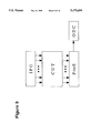
- FIG. 9 is a block diagram of a hardware model used to verify the performance of the invention.
- FIG. 10 is a block diagram of a two stage linear feedback shift register for checking two signatures.
- s n i.e., the ith signature s i is checked after l i bits of the sequence have been shifted into the LFSR.
- the check points are fixed, by logic simulation, one can easily determine the n corresponding fault-free signatures or references, r 1 , r 2 , . . . , r n .
- the ith signature s i is compared with its corresponding reference r i at the ith check point.
- the signatures and references must correspond on a one-to-one basis for a CUT to be declared good.
- CMS multiple signature
- FIG. 1 illustrates an implementation of such a prior art CMS scheme.
- ROM read only memory
- extra circuitry is required for generating ROM addresses and comparing ROM output with the signatures from the LFSR.
- extra circuitry requires more silicon area than the ROM itself. This is because implementing the address generator requires a form of counter, which is area-consuming compared to combinational circuits and ROM cells.
- comparing the references with the signatures requires either a parallel comparator or a serial comparator with some kind of parallel to serial converter to convert each k-bit reference into a serial k-bit sequence.
- a parallel comparator or a parallel to serial converter also takes considerable silicon area if k is not very small. Furthermore, connections among these functional blocks can also take much area.
- FMS Fuzzy Multiple Signature
- the FMS scheme also checks n signatures at check points, l 1 , l 2 , . . . , l n . But, unlike the CMS scheme where a signature s i is compared with a specific reference r i at check point l i , in the FMS scheme, each signature s i is compared with the whole set of references r 1 , r 2 , . . . , r n . A signature s i is considered good if it matches any of the references in the reference set.
- the FMS scheme for a CUT to be declared good, it suffices that the signature obtained from the LFSR at each check points corresponds to any of the references r 1 , r 2 , . . . , r n .
- the requirement for the one-to-one reference-to-signature correspondence is removed.
- This "fuzziness" introduced by allowing a multiple reference-to-signature correspondence may result in a small increase in aliasing compared to the CMS scheme for given k and n. But, this can be easily compensated for by the reduced complexity of the FMS scheme compared to the CMS scheme. Otherwise, the FMS scheme has all the advantages that the CMS scheme has over SS schemes.
- the FMS scheme requires a Signature Observer ("SO") and a LFSR.
- the LFSR collects signatures.
- the SO checks each signature, and generates Pass/Fail signals.
- the SO outputs a Pass signal, say logic 0. Otherwise, the SO outputs a Fail signal, say logic 1.
- the Fail signal can be fed to a test controller to terminate the testing and declare the CUT as faulty. If the SO outputs Pass signals at all of the predetermined check points, the CUT is declared good.
- the SO is a k-input, 1-output combinational circuit which outputs a 0 when its input vector belongs to the reference set, and outputs a 1 otherwise.
- the SO can be implemented with two 2-input NAND gates as shown in FIG. 3.
- the SO can be easily implemented with a k-input, 1-output, m-cube programmable logic array ("PLA"), or other non-PLA-type logic structures.
- PLA m-cube programmable logic array
- logic minimization can be used to reduce the area of the SO, as illustrated in Example 1.
- the number of references m that need to be included in the set of references can be reduced using the techniques described below, thereby reducing the hardware requirements of the SO.
- the number of aliased error sequences for such case is thus m ⁇ 2 l-k -1. Since there are 2 l -1 possible error sequences, assuming all are equally likely, the aliasing probability when m distinct references are acceptable at a single check point is: ##EQU3##
- the FMS scheme checks n signatures at check points l 1 , l 2 , . . . , l n against a set of m references, with m ⁇ n because there can be at most n distinct references if n signatures are checked. However, some references may happen to be, or be made identical, thus making m ⁇ n.
- L e FMS FMS scheme equivalent length
- P SS ⁇ 2 -k and P FMS ⁇ [n2 -k ] n P SS ⁇ 2 -k ] n
- L e CMS nk
- L e SS k
- L e FMS L e FMS -nlog 2 (n) for given n and k.
- the SS scheme requires a k-bit LFSR.
- the FMS scheme only requires a (k/n+log2(n)) bit LFSR plus the silicon area for the signature observer.
- a PLA implementation of the SO is assumed. Since each PLA input variable corresponds to two lines in the AND plane of a PLA, and since the drivers in the PLA take an area of about 8 cubes, the normalized area of a k-input, s-output, n-cube PLA is (n+8) ⁇ (k ⁇ 2+s) units.
- Area estimate comparisons are based on the actual layout of a PLA and a 16-bit LFSR, using the CadenceTM automatic place and route tool, and 3 um double-metal CMOS technology.
- the LFSR was built with static standard cell D flip-flops, and measured about 1.38 ⁇ 10 6 um 2 .
- the following example illustrates the comparison of the FMS and SS schemes.
- the required hardware is a 9-stage LFSR, and a 9-input, 1-output, 32-cube PLA to implement the SO.
- FIG. 5 More examples are summarized in FIG. 5, where the area for achieving a given aliasing probability is given in terms of equivalent LFSR sizes. As shown in FIG. 5, with the FMS scheme, small aliasing can be obtained against very small hardware overhead compared to what is required in the case of a SS scheme.
- the PLA is used to implement the ROM and comparator functions while the address generator is implemented using a log 2 n-bit counter if n signatures are checked.
- the PLA has k+log 2 n inputs, 1 output and n cubes.
- the PLA's inputs are the k-bit signature from the LFSR (as in the FMS scheme) and a log 2 n-bit index from the counter.
- the area overhead of the CMS scheme consists of the PLA and the counter.
- the area overhead is simply a k-input, 1-output, n-cube PLA that implements the SO if n k-bit signatures are checked.
- the area overhead of the FMS and CMS schemes will now be compared, given a desired aliasing probability.
- checking n signatures in the FMS scheme achieves the same aliasing probability P al as checking n-n/klog 2 n signatures in the CMS scheme.
- P al the number of signatures required can be determined for the FMS and CMS schemes respectively.
- the area required for the FMS and CMS schemes, respectively can be determined.
- a "zero" detector may be used, as shown in FIG. 7, to detect the Pass/Fail signal output by the SO.
- the "zero" detector Prior to testing a CUT, the "zero" detector is preset to "1", thus setting the Pass/Fail pin to 0.
- the controller temporarily sets the chk signal to 1. This sensitizes the "zero" detector to the SO output.
- a Fail signal (a "1" at the SO output) is detected, the detector outputs and keeps a Fail signal, "1", at the Pass/Fail pin.
- the "zero" detector can be shared by all self-testable blocks on an IC chip. When shared, the detector outputs and keeps a Fail signal if any of the self-testable blocks is found faulty. This Fail signal can be used to terminate testing, thereby reducing test time.
- test result of each self-testable block may consist of a single-bit flag stored in a status register. Once a faulty signature from a self-testable block is detected, the flag for the block is set. The status can be accessed through the IEEE 1149.1 Test Access Port. In this case, the flag can be used as the "zero" detector discussed above for the first case.
- the controller required for the FMS scheme is the same as for the CMS scheme. It will be shown that the hardware overhead of the FMS scheme's controller can be made as small as that required for the control of a SS scheme.
- an on-chip counter or LFSR (which may be simultaneously used for pseudo random pattern generation) is required to count the applied test vectors. When the final count is reached, a decoder detects this final count and generates a signal to stop the test and perform final signature evaluation.
- the check points are arbitrary, i.e., the test length between check points l i and l i+1 can be arbitrarily selected.
- an on-chip counter is required to count the applied test vectors.
- a decoder detects the corresponding count and outputs a chk signal to enable the evaluation of a signature.
- the decoder in this case must decode all the counts corresponding to the check points, and is thus considerably larger. This is the worst case in terms of hardware overhead among the possible implementations of the FMS scheme's controller.
- the scheduling of the check points follows a regular equidistant pattern, i.e., the test length between l i and l i+1 is constant for all i.
- a convenient constant is 2 q , where q is an integer.
- the counter required in the SS scheme is simply split into two smaller ones, say C 1 and C 2 .
- C 1 is a q-bit counter which counts the test length between two adjacent check points i.e., 2 q .
- C 2 counts the number of signatures to be checked. Assume the final count to be 0 for both C 1 and C 2 .
- a decoder decodes the 0 and generates the chk signal to enable the evaluation of a signature. If the signature is incorrect testing can be terminated and the CUT declared faulty. Otherwise, C 2 is decremented by 1, and testing continues. When both C 1 and C 2 reach the 0 state, the test is complete.
- the hardware requirement of the controller in this case is almost the same as that for the SS scheme since the total length of C 1 and C 2 is the same as that of the counter used in the SS scheme, and the total complexity of the two decoders to decode the 0's from C 1 and C 2 is the same as that of the decoder in the SS scheme. This is the best case in terms of hardware overhead among the possible implementations of the FMS scheme's controller.
- the third case lies between the first two, i.e., the check points are selected such that the test length between two adjacent check points, l i and l i+1 , is variable but constrained to values of 2 qi , where q i is an integer.
- counters C 1 and C 2 can again be used to count the applied test vectors.
- a LFSR random pattern generator can be shared as a counter to count the applied test vectors, e.g., as in the BIST controller of the Intel 80386 (see: Gelsinger, P. P, "Built In Self Test of the 80386," Proc. ICCD, 1986, pp. 169-173).
- the FMS control implementation described above applies equally well to the case where the conventional counter is replaced by a LFSR-type counter.
- the split of the LFSR into two smaller LFSR-based counters, C 1 and C 2 will not affect the randomness of the input pattern generator if concatenable polynomials are used (see: Bhavsar, D. K., "Concatenable Polydividers: Bit-sliced LFSR Chips for Board Self-Test," Proc. Int. Test Conf., 1985, pp. 88-93).
- FIG. 8 depicts the hardware model used, where "IPG” is an input pattern generator implemented with a LFSR, “ODC” is a output data compactor, and “MINSR” is a multiple input nonfeedback shift register that performs space compaction. Single stuck-at faults were assumed.
- an 8-bit primitive LFSR was used as the data compactor.
- the equidistant check point scheduling is the worst of the control strategies described in Section 4.2.
- the area requirement for the control of the FMS scheme in this case is the same as that required for a SS scheme.
- the corresponding hardware overhead in addition to that required for the SS scheme is about the size of a 2.16-bit LFSR.
- the total silicon area of the FMS scheme in the experiments is thus about equivalent to that of a 10.16-bit LFSR, as opposed to an 8-bit LFSR for the SS scheme.
- Table 1 shows the exact fault coverage before signature analysis (the "NC" column), and the coverage with the SS and the FMS schemes, respectively for a test length of 1,024 random vectors. In all cases, the coverage of the FMS scheme is either the same or very close to that of the no-compaction case, and higher than that of the SS scheme.
- Table 2 shows the CPU time required to perform the above fault simulations. From Table 2, the CPU time required to perform the fault simulations with the FMS scheme is always close to that of the no-compaction case, which constitutes a lower bound (see: Lambidonis, D., Agarwal, V. K., Ivanov, A. and Xavier, D., "Computation of Exact Fault Coverage for Compact Testing Schemes," Proc. ISCAS, June 1991, pp. 1873-1876). In the case of the SS scheme, however, the fault simulation time is always one order of magnitude longer. In Table 2, the column “Time Savings" shows the CPU time saved from using the FMS scheme rather than the SS scheme.
- the number of test vectors simulated is small, and the check point scheduling is the worst case in reducing fault simulation time. If longer test length, larger circuits, and optimal scheduling of the check points were considered, the fault simulation time saved from using the FMS scheme rather than a SS scheme would be even much more significant.
- checking n signatures requires n references. These references must be somehow stored in a ROM as in the CMS scheme, or built in the SO as in the FMS scheme. However, if all the references are made identical, say all equal to 0, then only one reference needs to be stored. Thus, the hardware requirement for checking identical multiple signatures can be as small as that for any single signature scheme, and is independent of the number of checked signatures. The control of the signature checking does not result in extra hardware overhead to the conventional BIST controller if the check points are equidistantly scheduled. Having one constant reference signature for all check points is a fundamental aspect of the invention. A technique for achieving identical reference signatures that does not entail any hardware overhead nor any circuit modification will now be discussed.
- the signatures are allowed to be any one of the 2 k possible values as long as they are identical, then this probability becomes 2 - (n-1)k. This probability is very small for practical values of n and k. Thus, in general, it is unlikely that the n signatures would be identical.
- the probability that one of these sequences yields n identical signatures at the predetermined check points can be very high. As shown above, given one sequence, the probability is 2 -nk+k . Given a choice between two sequences, the probability that at least one of the two yields n identical signatures follows a geometric distribution, i.e., the probability is 2 -nk+k +(1-2 -nk+k )2 -nk+k . Given L possible fault-free sequences, the probability that at least one of the sequences yields n identical k-bit signatures is: ##EQU5##
- C L ,n,k is a measure of confidence of finding at least one sequence from L sequences that yields n identical signatures. Obviously, C L ,n,k ⁇ 1 as L ⁇ . Therefore, n identical signatures can be highly probable if L can be made sufficiently large. The feasibility of this scheme rests upon how efficiently the L fault-free sequences can be obtained, as well as how large L must be, as discussed below.
- a simple way to generate L fault-free sequences is to apply L different sets of random vectors to the CUT and choose the set of random vectors that generates n identical signatures as the test vector set.
- To generate L sequences one may try L input pattern generator ("IPG") LFSRs with different feedback polynomials, or try L different seeds of the IPG LFSR.
- IPG L input pattern generator
- both of these methods imply simulating the CUT L times, each for l test vectors.
- the corresponding time complexity is O(l L ) (disregarding the dependency of the simulation on the CUT parameters), which may become unacceptable for large l and L.
- the above method for generating fault-free sequences can also be applied to the case where the P-to-S converter is a scan chain. With a scan chain of length m, each input vector yields m output bits to compact. In this case, the IPG LFSR requires only (l+L-1)/m shifts to generate L fault-free sequences. Thus, the sequence generation time complexity is only O( ⁇ l+L ⁇ / ⁇ m ⁇ ) if the P-to-S is a m-stage scan chain.
- a fault-free sequence of length l+L-1 yields a choice of L sequences of length l.
- Each of the latter sequences is actually a subsequence of the (l+L-1)-bit sequence.
- an efficient algorithm to search for an adequate subsequence of length l that yields identical signatures is now presented.
- the eight transient LFSR states, starting with seed (01), when the subsequence (1 1 0 1 0 1 1 0) is applied are shown below:
- C, L and k are directly related to the desired confidence, allowed CPU time overhead, and affordable hardware area, respectively.
- the expected number of identical signatures can be found by solving Eqnuation 10 for n.
- the aliasing probability is: ##EQU6## 6.4.2 CPU Time Overhead
- the CPU time required to implement the preferred embodiment involves two aspects. One is the effort in generating the L fault-free sequences; the other is the effort spent in searching an adequate sequence among the L sequences. With the algorithm presented above, the searching requires only a negligible amount of CPU time. Thus, the major CPU time required is that of generating the L fault-free sequences, which is in fact the CPU time required for simulating the fault-free CUT to get L-1 extra output bits. Disregarding the dependency of the simulation on the CUT parameters, the required CPU time for obtaining L-1 extra output bits is proportional to L. Similarly, the CPU time for simulating a CUT to get a l-bit fault-free sequence is proportional to l. Thus, the CPU time overhead is L/l relative to the effort required to generate an l-bit fault-free output sequence by logic simulation.
- the CPU time overhead can be further reduced by combining the logic simulation for fault-free sequence generation with the searching for identical signatures, i.e., generating a fault-free sequence and concurrently determining whether any of its subsequences generated so far yields n identical signatures. Once such a subsequence is found, the process terminates.
Abstract
A method of testing a digital integrated circuit for faults. A plurality of n check points l1, l2, . . . , ln are established to define a test sequence. A set of m references r1, r2, . . . , rm are predefined, corresponding to the signatures which the circuit would produce at the corresponding check points in the absence of any faults. A test sequence is applied to the circuit and an output signature si is derived from the circuit at the corresponding check point li. The output signature is compared with each member of the set of references. The circuit is declared "good" if the signature matches at least one member of the set of references, or "bad" if a signature matches no members of the set of references. Testing proceeds in similar fashion at the next check point, until the circuit has been tested at all check points.
Description
This application pertains to the testing of large scale digital integrated circuits for detection of circuit faults. A "fuzzy" multiple signature analysis approach eliminates the need for strict one-to-one correspondence between each signature obtained from the circuit under test and a reference signature. Signatures obtained from the circuit under test need only correspond to any one of a set of reference signatures.
Built-In Self-Test ("BIST") is an increasingly popular means of testing large scale digital integrated circuits ("ICs") for circuit faults. A test pattern is generated on the IC to be tested; and, output data obtained by subjecting the IC to the test pattern is evaluated on the IC itself. The output data evaluation generally consists of (i) data compaction, whereby the output sequences produced by the circuit under test ("CUT") are compacted into a single signature of a few bits, and (ii) comparison of the signature with a predetermined fault-free signature to determine whether the CUT is good. However, due to the information loss through data compaction, some error responses may be mapped to the fault-free signature, thus causing some faulty circuits to escape detection. This problem is called aliasing. Usually, fault coverage before compaction can be detected by fault simulation. But, fault coverage after data compaction can usually only be estimated since exact fault simulation is not computationally feasible for large circuits. Although many probabilistic techniques have been developed, they can not be used with confidence for a specific CUT because of statistical uncertainties.
At least two kinds of signature analysis have been proposed: single signature ("SS") analysis and multiple signature ("MS") analysis (see: Bardell, P. H., McAnney, W. H. and Savir, J., "Built-In Test for VLSI: Pseudorandom Techniques", John Wiley & Sons, Inc., 1987). In the SS scheme, only a single final signature is checked at the end of a test session. In the MS scheme, however, in addition to the final signature, some intermediate signatures are checked as well. The MS scheme is known to significantly reduce aliasing. Recently, it has been shown that, besides reducing aliasing, checking multiple signatures has many other advantages over the SS scheme. For example, by checking multiple signatures, exact fault coverage after data compaction can be easily computed for large CUTs by fault simulation. Average test time can be greatly reduced by checking multiple signatures since a faulty CUT's testing session can be terminated as soon as any incorrect intermediate signature is detected. Fault diagnosability also improves with multiple signatures.
A major problem with MS schemes is that they require complex implementation and large associated hardware overhead. In "A Multiple Signature Scheme for BIST", Proc. Cdn. Conf. on VLSI 1991, the present inventors proposed a multiple signature compaction scheme for BIST. By sharing some of the circuitry required by standard single signature BIST schemes, the scheme achieves very small aliasing at the expense of small silicon area. Unfortunately, the scheme's silicon area requirements increase with test length. This makes the scheme less attractive as CUTs get larger and require long test sets. The present invention provides a new output data compaction scheme for BIST which is simple to implement and requires little hardware overhead, even compared with SS schemes, and yet has all the advantages of conventional MS schemes.
In accordance with the preferred embodiment, the invention provides a method of testing a digital integrated circuit for faults. A plurality of n check points l1, l2, . . . in are established at specific points within the test output sequence. A set of m references r1, r2, . . . , rm are predefined. This set of m references includes at least all of the signatures which the circuit would produce at the corresponding check points in the absence of any fault or faults. A test sequence is applied to the circuit and an output signature si is derived from the circuit at the corresponding check point li. The output signature is compared with each member of the set of references. If the signature does not match any member of the set of references, the circuit is declared "bad" and testing may be terminated. If the signature matches any member of the reference set, testing proceeds in similar fashion to the next check point. The circuit may be declared "good" if the signature corresponding to each of the pre-defined check points matches at least one member of the reference set.
FIG. 1 is a block diagram representation of a conventional prior art multiple signature compaction scheme having a parallel comparator.
FIG. 2 is a block diagram representation of a multiple signature data compaction scheme in accordance with the present invention.
FIG. 3 depicts a three bit signature observer for use with references 111, 110 and 100.
FIG. 4 is a graph illustrating the aliasing performance of the invention.
FIG. 5 is a graphical comparison of the silicon area overhead requirements of a multiple signature data compaction scheme in accordance with the present invention with those of conventional single and multiple signature schemes.
FIG. 6 is a graphical comparison of the silicon area overhead requirements of a multiple signature data compaction scheme in accordance with the present invention with those of a conventional multiple signature scheme.
FIG. 7 is a schematic diagram of a detector circuit for detecting a Pass/Fail signal produced by a signature observer.
FIG. 8 is a block diagram of a hardware model used to study the fault coverage performance of a multiple signature data compaction scheme in accordance with the present invention.
FIG. 9 is a block diagram of a hardware model used to verify the performance of the invention.
FIG. 10 is a block diagram of a two stage linear feedback shift register for checking two signatures.
1.0 Conventional Signature Analysis
1.1 Single Signature Schemes
In BIST with signature analysis, to compact an output sequence, the sequence is shifted bit by bit into a signature analyzer implemented by a linear feedback shift register ("LFSR"). At the end of the test session, the contents of the LFSR form the signature. Denoting the output sequence length by l and the number of the LFSR stages by k, under the assumption of the equally likely error model of Bardell et al (supra) the aliasing probability Pal is: ##EQU1## Assuming l>>k yields Pal ≈2-k. This asymptotic result is well-known, and is also true for unequally likely error models.
1.2 Multiple Signature Schemes
Assuming the equally likely error model, it has been shown that if two signatures are checked, i.e., an intermediate signature after the first l1 bits of the sequence have been shifted into the signature analyzer, and a second signature at the end of the sequence of length l, then the aliasing probability is: ##EQU2##
Assuming l>>k yields Pal (2)≈2-2k. It is easy to prove that Pal (n)≈2-nk if n signatures are checked at positions l1, l2, . . . , ln, respectively, and assuming k<<l1 <l2 < . . . <ln =l, where li is the position of the ith signature. These positions are called "check points". Assume the n signatures generated by the LFSR at the check points l1, l2, . . . , ln are s1, s2, . . . , sn, i.e., the ith signature si is checked after li bits of the sequence have been shifted into the LFSR. Once the check points are fixed, by logic simulation, one can easily determine the n corresponding fault-free signatures or references, r1, r2, . . . , rn. When testing the CUT, the ith signature si is compared with its corresponding reference ri at the ith check point. Thus, in this prior art scheme, the signatures and references must correspond on a one-to-one basis for a CUT to be declared good. Such a one-to-one correspondence between specific references and signatures at specific check points makes conventional multiple signature ("CMS") schemes complicated and expensive to implement.
FIG. 1 illustrates an implementation of such a prior art CMS scheme. As shown, in addition to a read only memory ("ROM") for storing the n references, extra circuitry is required for generating ROM addresses and comparing ROM output with the signatures from the LFSR. Usually, such extra circuitry requires more silicon area than the ROM itself. This is because implementing the address generator requires a form of counter, which is area-consuming compared to combinational circuits and ROM cells. Also, comparing the references with the signatures requires either a parallel comparator or a serial comparator with some kind of parallel to serial converter to convert each k-bit reference into a serial k-bit sequence. A parallel comparator or a parallel to serial converter also takes considerable silicon area if k is not very small. Furthermore, connections among these functional blocks can also take much area.
2.0 Fuzzy Multiple Signature Analysis
As mentioned above, the complexity of checking multiple signatures is mainly due to the need for one-to-one correspondence between the references and signatures. Removal of this strict requirement significantly simplifies the data compactor. This essential concept, which underlies the present invention, is referred to as a Fuzzy Multiple Signature ("FMS") scheme since it consists of checking multiple signatures, without requiring one-to-one correspondence between each reference and signature.
2.1 Basis
Like the CMS scheme, the FMS scheme also checks n signatures at check points, l1, l2, . . . , ln. But, unlike the CMS scheme where a signature si is compared with a specific reference ri at check point li, in the FMS scheme, each signature si is compared with the whole set of references r1, r2, . . . , rn. A signature si is considered good if it matches any of the references in the reference set. Therefore, in the FMS scheme, for a CUT to be declared good, it suffices that the signature obtained from the LFSR at each check points corresponds to any of the references r1, r2, . . . , rn. Thus, in the FMS scheme, the requirement for the one-to-one reference-to-signature correspondence is removed. This "fuzziness" introduced by allowing a multiple reference-to-signature correspondence may result in a small increase in aliasing compared to the CMS scheme for given k and n. But, this can be easily compensated for by the reduced complexity of the FMS scheme compared to the CMS scheme. Otherwise, the FMS scheme has all the advantages that the CMS scheme has over SS schemes.
2.2 Implementation
Since one-to-one correspondence between references and signatures is unecessary, implementing the FMS scheme is very simple. As shown in FIG. 2, the FMS scheme requires a Signature Observer ("SO") and a LFSR. The LFSR collects signatures. The SO checks each signature, and generates Pass/Fail signals. At each check point, if the signature generated by the LFSR matches any of the references, the SO outputs a Pass signal, say logic 0. Otherwise, the SO outputs a Fail signal, say logic 1. The Fail signal can be fed to a test controller to terminate the testing and declare the CUT as faulty. If the SO outputs Pass signals at all of the predetermined check points, the CUT is declared good. The SO is a k-input, 1-output combinational circuit which outputs a 0 when its input vector belongs to the reference set, and outputs a 1 otherwise.
Assume n=k=3, i.e., to check three 3-bit signatures. If the references are r1 =111, r2 110, and r3 =100, denoting the three bits of the references by b1, b2, and b3, respectively, the function of the SO can be described as:
Pass/Fail=b.sub.1 b.sub.2 b.sub.3 +b.sub.1 b.sub.2 b.sub.3 +b.sub.1 b.sub.2 b.sub.3 =b.sub.1 b.sub.2 +b.sub.1 b.sub.3 = (3)
Thus, the SO can be implemented with two 2-input NAND gates as shown in FIG. 3.
In general, to check n k-bit signatures, the SO can be easily implemented with a k-input, 1-output, m-cube programmable logic array ("PLA"), or other non-PLA-type logic structures. However, logic minimization can be used to reduce the area of the SO, as illustrated in Example 1. Furthermore, the number of references m that need to be included in the set of references can be reduced using the techniques described below, thereby reducing the hardware requirements of the SO.
2.3 FMS Aliasing Performance Analysis
Assume the compaction of a l-bit random sequence into a k-bit signature, and r1 to be the only valid reference. The total number of sequences (including the fault-free one) that map to r1 is 2l-k. If it is assumed that distinct references r1 and r2 are both acceptable, then the total number of sequences that map to either r1 or r2 is 2×2l-k since the sequences that map to one will not map to the other. Thus, assuming that m distinct references, r1, r2, . . . , rm are acceptable, the total number of l-bit sequences that map to any one of the m references is m×2l-k. Excluding the fault-free sequence, the number of aliased error sequences for such case is thus m×2l-k -1. Since there are 2l -1 possible error sequences, assuming all are equally likely, the aliasing probability when m distinct references are acceptable at a single check point is: ##EQU3##
Assuming l>>k yields Pal ≈m2-k.
The FMS scheme checks n signatures at check points l1, l2, . . . , ln against a set of m references, with m≦n because there can be at most n distinct references if n signatures are checked. However, some references may happen to be, or be made identical, thus making m<n. Using the arguments presented above in Section 1.2 for the aliasing probability of CMS schemes, the following aliasing probability results for the FMS scheme: ##EQU4## where li is the ith check point.
Assuming li >>k yields:
P.sub.FMS ≈[m2.sup.-k ].sup.n (6)
Clearly, for fixed k and n, the best-case aliasing occurs for m=1. The worst case aliasing occurs when m=n, for which PFMS ≈[n2-k ]n.
The following analysis assumes the worst-case scenario (i.e., m=n). To study the aliasing performance of the FMS scheme a "FMS scheme equivalent length" Le FMS is defined as a figure of merit. For a given aliasing probability in the FMS scheme, define Le FMS to be the length of a LFSR that yields the same aliasing probability in a SS scheme. Ideally, Le FMS should be as large as possible to minimize aliasing. Assume Le FMS to be a continuous variable. Since PSS ≈2-k and PFMS ≈[n2-k ]n, then
2.sup.-L.sbsp.e.spsp.FMS ≈[n2.sup.-k ].sup.n (7)
Solving for Le FMS yields:
L.sub.e.sup.FMS =n(k-log.sub.2 (n)) (8)
In comparison, the equivalent length of a CMS scheme is Le CMS =nk; while that of a SS scheme is Le SS =k. Thus, Le FMS =Le FMS -nlog2 (n) for given n and k.
Assuming k=16 and n=4, Le SS =16, Le CMS =64, and Le FMS =64-4×2=56. Thus, PCMS =2-64, PFMS =2-56, and PSS =2-16. Here, the aliasing probability of the FMS scheme is 2 orders of magnitude greater than that of the CMS scheme, but still 12 orders of magnitude smaller than that of the SS scheme.
With the CMS scheme, the equivalent length increases linearly with both k and n. With the FMS scheme, however, the equivalent length increases linearly with k but not with n. For fixed k, as n increases, Le FMS peaks and then decreases. When n=2k, Le FMS =0. FIG. 4 shows an example of the Le FMS as a function of n for k=8, k=9, k=12 and k=16.
3.0 Comparative Evaluation of the FMS Scheme
The aliasing performance and hardware requirements of the FMS scheme will now be compared with those of the SS and CMS schemes, respectively. The worst case of the FMS scheme, i.e., m=n is again considered, and no logic minimization is performed for the SO's function.
3.1 FMS vs. SS
To achieve an aliasing probability of 2-k, the SS scheme requires a k-bit LFSR. To achieve the same aliasing probability, the FMS scheme only requires a (k/n+log2(n)) bit LFSR plus the silicon area for the signature observer. For the following more detailed area comparisons, a PLA implementation of the SO is assumed. Since each PLA input variable corresponds to two lines in the AND plane of a PLA, and since the drivers in the PLA take an area of about 8 cubes, the normalized area of a k-input, s-output, n-cube PLA is (n+8)×(k×2+s) units. Area estimate comparisons are based on the actual layout of a PLA and a 16-bit LFSR, using the Cadence™ automatic place and route tool, and 3 um double-metal CMOS technology. The LFSR was built with static standard cell D flip-flops, and measured about 1.38×10⁶ um2. Actual layout revealed that a 12-input, 4-output, 64-cube PLA takes about the same area as a 16-bit LFSR. According to the above analysis, this PLA requires an area of (64+8)×(12×2+4)=2016 units. Therefore, it is assumed that a PLA of 2016 units corresponds to the area of a 16-bit LFSR. The following example illustrates the comparison of the FMS and SS schemes.
If k=9 and n=32, PFMS =[32×2-9 ]32 =2-128. In this case, the required hardware is a 9-stage LFSR, and a 9-input, 1-output, 32-cube PLA to implement the SO. The PLA requires (32+8)×(9×2+1)=760 units of area, which is about 37.7% of the size of a 16-bit LFSR, or about the size of a 6-bit LFSR. Thus, the total area overhead for the FMS scheme to achieve PFMS =2-128 is approximately the area of a 6+9=15 bit LFSR. In comparison, a SS scheme would require a 128-bit LFSR to achieve PSS =2-128. More examples are summarized in FIG. 5, where the area for achieving a given aliasing probability is given in terms of equivalent LFSR sizes. As shown in FIG. 5, with the FMS scheme, small aliasing can be obtained against very small hardware overhead compared to what is required in the case of a SS scheme.
3.2 FMS VS. CMS
To simplify the comparison of the FMS and CMS schemes, for the CMS scheme assume a PLA is used to implement the ROM and comparator functions while the address generator is implemented using a log2 n-bit counter if n signatures are checked. To check n k-bit signatures with the CMS scheme, the PLA has k+log2 n inputs, 1 output and n cubes. The PLA's inputs are the k-bit signature from the LFSR (as in the FMS scheme) and a log2 n-bit index from the counter. Here, one need only measure the area overhead beyond that required by a SS scheme (in other words, the area of the LFSR is not measured, since it is the same for both the FMS and CMS schemes). Thus, the area overhead of the CMS scheme consists of the PLA and the counter. For the FMS scheme, the area overhead is simply a k-input, 1-output, n-cube PLA that implements the SO if n k-bit signatures are checked. The area overhead of the FMS and CMS schemes will now be compared, given a desired aliasing probability.
From the analysis in Section 2.2, for a given signature length k, checking n signatures in the FMS scheme achieves the same aliasing probability Pal as checking n-n/klog2 n signatures in the CMS scheme. Thus, given k and a desired Pal, the number of signatures required can be determined for the FMS and CMS schemes respectively. Then, using a calculation similar to that used in Section 3.1, the area required for the FMS and CMS schemes, respectively can be determined.
FIG. 6 illustrates the area overhead of the FMS and CMS schemes for k=8 and k=12. In FIG. 6, the area overhead is given in terms of equivalent LFSR sizes. From FIG. 6, when k=8, the FMS scheme requires less area overhead, compared to the CMS scheme, as Pal >2-120. When k=12, and for Pal greater than 2-500 approximately, the FMS scheme requires less area overhead than the CMS scheme. If k=16, for Pal greater than about 2-1000 approximately, the FMS scheme requires less overhead also. For a fixed k, when Pal is smaller than a certain value, the area overhead of the FMS scheme becomes higher. This is because the aliasing probability of the FMS scheme is not a linear function of n when k is fixed (see FIG. 4).
4.0 Observation and Control
4.1 Test Result Observation
Two different cases are considered for observation of the test results. First, if there is a Pass/Fail pin available, a "zero" detector may be used, as shown in FIG. 7, to detect the Pass/Fail signal output by the SO. Prior to testing a CUT, the "zero" detector is preset to "1", thus setting the Pass/Fail pin to 0. When a signature is checked, the controller temporarily sets the chk signal to 1. This sensitizes the "zero" detector to the SO output. Once a Fail signal (a "1" at the SO output) is detected, the detector outputs and keeps a Fail signal, "1", at the Pass/Fail pin. The "zero" detector can be shared by all self-testable blocks on an IC chip. When shared, the detector outputs and keeps a Fail signal if any of the self-testable blocks is found faulty. This Fail signal can be used to terminate testing, thereby reducing test time.
In the second case, where a specific protocol for control and observation of BIST is available (see, for example, Scholz, H. et al., "ASIC Implementations of Boundary-Scan and BIST," Int. Custom Microelectronics Conf., London, UK, Nov. 1988, pp. 43.0-43.9) the test result of each self-testable block may consist of a single-bit flag stored in a status register. Once a faulty signature from a self-testable block is detected, the flag for the block is set. The status can be accessed through the IEEE 1149.1 Test Access Port. In this case, the flag can be used as the "zero" detector discussed above for the first case.
4.2 Control Implementation
The controller required for the FMS scheme is the same as for the CMS scheme. It will be shown that the hardware overhead of the FMS scheme's controller can be made as small as that required for the control of a SS scheme. For the control of a SS scheme, an on-chip counter or LFSR (which may be simultaneously used for pseudo random pattern generation) is required to count the applied test vectors. When the final count is reached, a decoder detects this final count and generates a signal to stop the test and perform final signature evaluation.
For the control of the FMS scheme, three possible cases are considered, depending on the scheduling of the check points. In the first case, the check points are arbitrary, i.e., the test length between check points li and li+1 can be arbitrarily selected. To control the FMS scheme, like the SS scheme, an on-chip counter is required to count the applied test vectors. When a check point is reached, a decoder detects the corresponding count and outputs a chk signal to enable the evaluation of a signature. Unlike a SS scheme's controller where the decoder detects only the final count, the decoder in this case must decode all the counts corresponding to the check points, and is thus considerably larger. This is the worst case in terms of hardware overhead among the possible implementations of the FMS scheme's controller.
In the second case, the scheduling of the check points follows a regular equidistant pattern, i.e., the test length between li and li+1 is constant for all i. A convenient constant is 2q, where q is an integer. To control the FMS scheme in this case, the counter required in the SS scheme is simply split into two smaller ones, say C1 and C2. C1 is a q-bit counter which counts the test length between two adjacent check points i.e., 2q. C2 counts the number of signatures to be checked. Assume the final count to be 0 for both C1 and C2. Every time C1 decrements to 0, a decoder decodes the 0 and generates the chk signal to enable the evaluation of a signature. If the signature is incorrect testing can be terminated and the CUT declared faulty. Otherwise, C2 is decremented by 1, and testing continues. When both C1 and C2 reach the 0 state, the test is complete. The hardware requirement of the controller in this case is almost the same as that for the SS scheme since the total length of C1 and C2 is the same as that of the counter used in the SS scheme, and the total complexity of the two decoders to decode the 0's from C1 and C2 is the same as that of the decoder in the SS scheme. This is the best case in terms of hardware overhead among the possible implementations of the FMS scheme's controller.
The third case lies between the first two, i.e., the check points are selected such that the test length between two adjacent check points, li and li+1, is variable but constrained to values of 2qi, where qi is an integer. In this case, counters C1 and C2 can again be used to count the applied test vectors. C1 must be of length qs, where qs =min qi. Two decoders are required. One decodes the 0 state from C1, while the other decodes the counts of 2qi-qs from C2, i=1, . . . , n-1. Every time C1 reaches 0, and C2 reaches 2qi-qs, i ε (1, . . . , n-1), a signature is checked. The hardware overhead in this case is between that of the first two cases, since the decoder for C1 detects only one count, but the decoder for C.sub. 2 has to detect n counts corresponding to the check points.
The foregoing assumes a counter for controlling the FMS scheme. A LFSR random pattern generator can be shared as a counter to count the applied test vectors, e.g., as in the BIST controller of the Intel 80386 (see: Gelsinger, P. P, "Built In Self Test of the 80386," Proc. ICCD, 1986, pp. 169-173). The FMS control implementation described above applies equally well to the case where the conventional counter is replaced by a LFSR-type counter. The split of the LFSR into two smaller LFSR-based counters, C1 and C2, will not affect the randomness of the input pattern generator if concatenable polynomials are used (see: Bhavsar, D. K., "Concatenable Polydividers: Bit-sliced LFSR Chips for Board Self-Test," Proc. Int. Test Conf., 1985, pp. 88-93).
5.0 Fault Simulation Experiments
To study the fault coverage performance of the FMS scheme, exact fault simulation of the ISCAS'85 benchmark circuits (see: Brglez, F. and Fujiwara, H., "A Neutral Netlist of 10 Combinational Benchmark Circuits and a Target Translator in FORTRAN," Proc. IEEE Int. Symp. Circuits and Systems, 1985, pp. 151-158) were performed with output data compaction. FIG. 8 depicts the hardware model used, where "IPG" is an input pattern generator implemented with a LFSR, "ODC" is a output data compactor, and "MINSR" is a multiple input nonfeedback shift register that performs space compaction. Single stuck-at faults were assumed. In the case of the SS scheme, an 8-bit primitive LFSR was used as the data compactor. For the FMS scheme, 8 signatures were checked at equidistant check points, and each was generated by the 8-bit LFSR, i.e., k=8 and n=8. In terms of fault simulation time reduction, the equidistant check point scheduling is the worst of the control strategies described in Section 4.2. But the area requirement for the control of the FMS scheme in this case is the same as that required for a SS scheme. The corresponding hardware overhead in addition to that required for the SS scheme is about the size of a 2.16-bit LFSR. The total silicon area of the FMS scheme in the experiments is thus about equivalent to that of a 10.16-bit LFSR, as opposed to an 8-bit LFSR for the SS scheme.
Table 1 shows the exact fault coverage before signature analysis (the "NC" column), and the coverage with the SS and the FMS schemes, respectively for a test length of 1,024 random vectors. In all cases, the coverage of the FMS scheme is either the same or very close to that of the no-compaction case, and higher than that of the SS scheme.
              TABLE 1
______________________________________
Circuit    No.     Fault-Coverage (%)
Name       Fault   NC         FMS   SS
______________________________________
C432        562    99.24      99.244
                                    99.11
C499        732    98.90      98.907
                                    97.95
C880       1171    95.64      95.645
                                    95.38
C1355      1820    98.64      98.640
                                    98.13
C1908      2015    94.65      94.615
                                    93.69
C2670      2781    82.65      82.659
                                    82.05
C3540      4035    93.45      93.451
                                    93.33
C5315      5982    96.23      96.230
                                    96.17
C7552      8408    93.01      93.010
                                    n/a
______________________________________
Table 2 shows the CPU time required to perform the above fault simulations. From Table 2, the CPU time required to perform the fault simulations with the FMS scheme is always close to that of the no-compaction case, which constitutes a lower bound (see: Lambidonis, D., Agarwal, V. K., Ivanov, A. and Xavier, D., "Computation of Exact Fault Coverage for Compact Testing Schemes," Proc. ISCAS, June 1991, pp. 1873-1876). In the case of the SS scheme, however, the fault simulation time is always one order of magnitude longer. In Table 2, the column "Time Savings" shows the CPU time saved from using the FMS scheme rather than the SS scheme. Here, the number of test vectors simulated is small, and the check point scheduling is the worst case in reducing fault simulation time. If longer test length, larger circuits, and optimal scheduling of the check points were considered, the fault simulation time saved from using the FMS scheme rather than a SS scheme would be even much more significant.
              TABLE 2
______________________________________
Circuit  No of    Fault Simulation Time
                                    Time
Name     Faults   NC      FMS    SS     Sav
______________________________________
C432     562      2.25    6.96   48.90  85.77%
C499     732      3.70    11.32  72.64  84.42%
C880     1171     14.30   34.26  191.37 82.10%
C1355    1820     29.39   64.54  380.36 83.03%
C1908    2015     63.66   108.00 465.29 76.79%
C2670    2781     202.5   361.37 124    70.91%
C3540    4035     268.2   420.38 1823.  76.95%
C5315    5982     419.8   841.02 499    83.15%
C7552    8408     126     1865.72
                                 n/a    n/a
______________________________________
6.0 Multiple Signature Analysis with a Single Reference
6.1 Basis of the Scheme
Usually, checking n signatures requires n references. These references must be somehow stored in a ROM as in the CMS scheme, or built in the SO as in the FMS scheme. However, if all the references are made identical, say all equal to 0, then only one reference needs to be stored. Thus, the hardware requirement for checking identical multiple signatures can be as small as that for any single signature scheme, and is independent of the number of checked signatures. The control of the signature checking does not result in extra hardware overhead to the conventional BIST controller if the check points are equidistantly scheduled. Having one constant reference signature for all check points is a fundamental aspect of the invention. A technique for achieving identical reference signatures that does not entail any hardware overhead nor any circuit modification will now be discussed.
6.2 Achieving Identical Reference Signatures
Assume a set of random vectors is applied to a fault-free CUT such that a fault-free sequence of length l results. Assume the checking of n k-bit signatures at the predetermined check points l1, l2, . . . , ln (these check points can be arbitrary). For a fault-free sequence, if it is assumed that each of the sequence bits is statistically independent and equally likely to be 0 or 1, then the probability for each signature to be equal to a given value, say equal to 0 . . . 0, is 2-k. Thus, for such a arbitrary fault-free sequence, the probability that all signatures be identical and equal to a specific value is 2-nk. If the value of the single reference is unrestricted, i.e., the signatures are allowed to be any one of the 2k possible values as long as they are identical, then this probability becomes 2-(n-1)k. This probability is very small for practical values of n and k. Thus, in general, it is unlikely that the n signatures would be identical.
However, if there exists a choice of many different fault-free sequences, which is possible by applying different sets of random vectors to the CUT, then the probability that one of these sequences yields n identical signatures at the predetermined check points can be very high. As shown above, given one sequence, the probability is 2-nk+k. Given a choice between two sequences, the probability that at least one of the two yields n identical signatures follows a geometric distribution, i.e., the probability is 2-nk+k +(1-2-nk+k)2-nk+k. Given L possible fault-free sequences, the probability that at least one of the sequences yields n identical k-bit signatures is: ##EQU5##
The probability CL,n,k is a measure of confidence of finding at least one sequence from L sequences that yields n identical signatures. Obviously, CL,n,k →1 as L→∞. Therefore, n identical signatures can be highly probable if L can be made sufficiently large. The feasibility of this scheme rests upon how efficiently the L fault-free sequences can be obtained, as well as how large L must be, as discussed below.
6.3 Sequence Generation and Selection
As shown above, L will in practice tend to be large. Thus, successful implementation of the invention depends on the efficiency of generating the fault-free sequences by logic simulation, and of searching the sequences for one that yields identical signatures. Techniques for these tasks will now be described.
6.3.1 Efficient Generation of Fault-Free Sequences
A simple way to generate L fault-free sequences is to apply L different sets of random vectors to the CUT and choose the set of random vectors that generates n identical signatures as the test vector set. To generate L sequences, one may try L input pattern generator ("IPG") LFSRs with different feedback polynomials, or try L different seeds of the IPG LFSR. However, both of these methods imply simulating the CUT L times, each for l test vectors. Thus, the corresponding time complexity is O(lL) (disregarding the dependency of the simulation on the CUT parameters), which may become unacceptable for large l and L. A more efficient technique is presented next.
First, consider the case where the P-to-S converter in FIG. 9 is such that every input pattern to the CUT results in a single bit output, i.e., l patterns yield l output bits. Denote the fault-free output sequence by b1, b2, . . . , bl. Shifting the IPG LFSR one more time, which is equivalent to simulating the CUT for a total of l+1 test vectors, yields one more output bit bl+1. From the (l+1)-bit sequence, there exists two possible sequences of 1 consecutive bits. One is the sequence b1, b2, . . . , bl. The other is b2, b3, . . . , bl+1. These two sequences are very unlikely to be the same since the probability for the two sequences to be identical is extremely small (approximately 2-l). Clearly, shifting the IPG LFSR L-1 more times, i.e., simulating the CUT with a total of l+L-1 test vectors, yields l+L-1 output bits, b1, b2, . . . , bl+L-1. Such a l+L-1 bit sequence yields the choice of L fault-free sequences of length l. The time complexity of this generation technique is only O(l+L), which is simply a linear increase in the necessary time to generate a single l-bit fault-free output sequence.
The above method for generating fault-free sequences can also be applied to the case where the P-to-S converter is a scan chain. With a scan chain of length m, each input vector yields m output bits to compact. In this case, the IPG LFSR requires only (l+L-1)/m shifts to generate L fault-free sequences. Thus, the sequence generation time complexity is only O({l+L}/{m}) if the P-to-S is a m-stage scan chain.
6.3.2 Adequate Sequence Selection
As shown above, a fault-free sequence of length l+L-1 yields a choice of L sequences of length l. Each of the latter sequences is actually a subsequence of the (l+L-1)-bit sequence. Given a (l+L-1)-bit fault-free sequence, an efficient algorithm to search for an adequate subsequence of length l that yields identical signatures is now presented.
The following example shows the basic concept of the way in which an adequate sequence can be selected.
Example: Use the 2-stage LFSR shown in FIG. 10 to check 2 signatures. Assume the initial state of the LFSR is (00), l=8, and L=4. If l1 =4, and l2 =l=8, i.e., check a signature after every four bits being shifted into the LFSR. Given the (l+L-1)-bit sequence to compact as:
1 1 1 1 0 1 0 1 1 0 0
the eleven transient LFSR states after every shift are shown below:
(10 ) (01) (00)(10) (11) (11) (0) (00) (10) (11) (01)
An examination of the transient states shows that starting with the seed (01) the 8-bit subsequence (1 1 0 1 0 1 1 0) would yield two identical signatures at l1 =4 and l2 =8. The value of the signatures is (11). The eight transient LFSR states, starting with seed (01), when the subsequence (1 1 0 1 0 1 1 0) is applied are shown below:
(00) (10) (11) (11) (01) (00) (10) (11)
In the above example, all the transient LFSR states are pre-calculated and stored. Storing these states may require a large memory space. An efficient searching algorithm which is based on a similar idea as shown in the example, but which avoids the requirement of storing these transient states, will now be described. Assume the (l+L-1)-bit fault-free sequence is M=b1, b2, . . . , bl+L-1, where b1 is the first bit to compact. To simplify the algorithm, denote the initial seed to the signature LFSR by s0. The searching algorithm is shown in the following pseudo-procedure:
______________________________________
search.process(M, L, n, k, l.sub.1, l.sub.2, ..., l.sub.n)
seed = s.sub.0 = 0; l.sub.0 = 0;
         for(i=1 to n) do
           initialize the signature LFSR with seed;
           j = i - 1;
           calculate the signature s.sub.i by shifting the
           sequence bits
           b.sub.lj+1, b.sub.lj+2, ..., b.sub.lj+li into the LFSR;
           seed = s.sub.i ;
         endoffor
         i = 1;
         while((the signatures s.sub.1, s.sub.2, ..., s.sub.n are not
         identical)&&(i ≦ L)) do
           for(j = 0 to n) do
             initialize the signature LFSR to the
             value of s.sub.j ;
             calculate a new s.sub.j by shifting bit b.sub.i+lj
             into the signature LFSR;
           endoffor
           i = i + 1;
         endofwhile
         if(i > L) then print "fail to find an adequate
         sequence";
         else print the results i, the value of the signa-
         tures, and the signature LFSR seed that results
         in the identical signatures, i.e., s.sub.0 ;
endofsearch.
______________________________________
This search is very fast, and takes little memory. For example, when l=216 and L=22 20, the search takes only a few seconds on a Sun SparcStation™ 2.
6.4 Feasibility and Aliasing Performance of the Scheme
The magnitude of L required to ensure certain confidence for successfully using the invention (i.e. the amount of CPU time overhead required to implement the invention) is now discussed.
6.4.1 Required L vs. Aliasing Performance of the Scheme
Given n, k, and a desired confidence C of success in finding an adequate sequence, the required L can be obtained by solving Equation 10 with CL,n,k =C. Some results are shown in Table 3:
TABLE 3 ______________________________________ L C (%) ______________________________________ 2.sup.nk-k+ 1 86.47 2.sup.nk-k+2 98.17 2.sup.nk-k+3 99.97 ______________________________________
From Table 1, if nk-k=16, L=217 is required to ensure 86% confidence, and L=218 is required for a confidence of 98%. With nk-k=16, some examples of n, k, and corresponding aliasing probability Pat, are shown in Table 4.
              TABLE 4
______________________________________
k               n           P.sub.a1
______________________________________
1               17          2.sup.-17
2               9           2.sup.-18
4               5           2.sup.-20
8               3           2.sup.-24
16              2           2.sup.-32
______________________________________
From Tables 3 and 4, if L=217, one has 86% confidence of finding five identical signatures each of length 4, which corresponds to an aliasing probability Pal =2-20 ; or, with the same confidence, one can find two identical 16-bit signatures thus Pal =2-32. If L=218, the confidence goes up to 98%.
C, L and k are directly related to the desired confidence, allowed CPU time overhead, and affordable hardware area, respectively. Given C, L and k, the expected number of identical signatures can be found by solving Eqnuation 10 for n. In terms of these parameters, the aliasing probability is: ##EQU6## 6.4.2 CPU Time Overhead
The CPU time required to implement the preferred embodiment involves two aspects. One is the effort in generating the L fault-free sequences; the other is the effort spent in searching an adequate sequence among the L sequences. With the algorithm presented above, the searching requires only a negligible amount of CPU time. Thus, the major CPU time required is that of generating the L fault-free sequences, which is in fact the CPU time required for simulating the fault-free CUT to get L-1 extra output bits. Disregarding the dependency of the simulation on the CUT parameters, the required CPU time for obtaining L-1 extra output bits is proportional to L. Similarly, the CPU time for simulating a CUT to get a l-bit fault-free sequence is proportional to l. Thus, the CPU time overhead is L/l relative to the effort required to generate an l-bit fault-free output sequence by logic simulation.
Assuming an output sequence length l=220, which is not too long in practice, especially when a scan chain is used, yields 12.5% CPU time overhead for L=217, and 25% overhead for L=218. For example, with 25% CPU time overhead, there is over 98% confidence of achieving Pal =2-20 with k=8, or Pal =2-32 with k=16. Such percentages of CPU time overhead are acceptable in practice. For example, it takes only 0.2 minutes to simulate a 40,000 gate fault-free CUT with 220 test vectors. Thus, in this case, L=218 means only 3 seconds of extra CPU time. When only a fault-free sequence is required, simulation techniques based on higher-level circuit descriptions, e.g., functional or behavioral level descriptions, can be used, thus making the simulation process much faster. In some cases, if some "proven" fault-free circuits ("golden circuits") are available, the required fault-free sequence can be obtained by running these circuits.
The CPU time overhead can be further reduced by combining the logic simulation for fault-free sequence generation with the searching for identical signatures, i.e., generating a fault-free sequence and concurrently determining whether any of its subsequences generated so far yields n identical signatures. Once such a subsequence is found, the process terminates. In this case, the average CPU time overhead can be significantly reduced, since the average number of extra output bits that must be generated is much smaller than L. This average number is 2k-k, which is the mean value of a random variable characterized by a geometric distribution with parameter 2-nk+k [10]. For the cases shown in Table 4, where nk-k=16, the average CPU time overhead can be reduced to 6.25% from 12.5% or 25%.
6.5 Special Case: k=1
A special case arises for k=1, which yields Pal =2-n if n 1-bit signatures are checked. In this case, the hardware requirement is only a 1-stage LFSR. Moreover, the storage of the single reference required in the general case can be avoided if the state of the 1-stage LFSR at each check point is directly used as a go/nogo signal. The case where k=1 can be considered as a minimal hardware requirement for signature analysis.
When Pal =2-n is desired, from Table 3, L=2n is required to ensure 86% confidence, or L=2n+1 for a confidence of over 98%. Theoretically, with a 1-stage LFSR, the invention can achieve arbitrarily small aliasing if L is sufficiently large. Assuming k=1 and l=220, achieving the typical aliasing probability of 2-16 requires 6.25% CPU time overhead for 86% confidence, or 12.5% overhead for 98% confidence. Similarly to the discussion above, the average CPU time overhead in this case is only 3.125%.
7.0 Experimental Results for Achieving Identical References
To verify the feasibility of the invention, 150 experiments on the ISCAS'85 benchmark circuits (Brglez et al, supra) were performed. In the experiments, a multiple input nonfeedback shift register ("MINSR") was used as the P-to-S converter shown in FIG. 9. The signatures are checked at equidistant check points. This makes the corresponding hardware requirements for the control of checking multiple signatures as small as that for the control of any single signature scheme. In the experiments, for each given set of n and k, three trials were performed with each of the circuits. Table 5 shows the experimental results when nk-k=16:
              TABLE 5
______________________________________
        Log.sub.2 of the number of extra output bits
Circuit   n = 17,  n = 9,  n = 5,
                                 n = 3,
                                       n = 2,
Name      k = 1    k = 2   k = 4 k = 8 k = 16
______________________________________
C432      15.79    14.94   16.19 15.87 17.01
C499      14.07    15.29   15.72 14.65 15.08
C880      16.49    16.15   14.46 15.61 16.27
C1355     14.07    15.29   15.72 14.65 15.08
C1908     15.86    15.57   16.36 15.81 16.08
C2670     16.95    15.36   15.64 16.21 14.06
C3540     15.46    14.50   17.22 15.08 17.26
C5315     14.38    17.21   16.49 16.68 15.60
C6288     16.79    15.35   15.64 16.23 15.34
C7552     16.98    16.87   16.67 16.50 15.72
averages  15.68    15.65   16.01 15.73 15.75
Average = 15.76
______________________________________
As shown in Table 5, to find 17 identical 1-bit signatures, yielding Pal =2-17, requires the generation of 215.68 extra output bits on average. To find 2 identical 16-bit signatures thus yielding Pal =2-32, requires 215.75 extra output bits on average. Theoretically, the average number of extra output bits that must be generated is 2nk-k =216. In comparison, the last row of Table 5 shows that the average number of the required extra output bits over the 150 experiments is 215.76. This result is very close to the theoretical expectation. If l=220, 216 extra output bits translates into a CPU time overhead of only 6.25%, and 215.76 represents a CPU time overhead of 5.29%.
8.0 A General Technique to Reduce m
The foregoing techniques for generating fault-free sequences can be used not only to select an adequate sequence but also to reduce the number of references in the FMS scheme, i.e., to make 1<m<n, as will now be explained.
The FMS scheme eliminates the one-to-one correspondence between the references and the checked signatures. This makes it possible to can use fewer references than signatures, i.e., m<n. In this case, n-m of the n references used in the conventional case are made identical. To do so, the techniques described above for fault-free sequence generation can be used. A suitable technique for adequate sequence selection will now be described. Assume the (L+l-1)-bit fault-free sequence to be M=b1, b2, . . . , bl+L-1, where b1 is the first bit to compact. To simplify the algorithm, denote the initial seed to the signature LFSR by s0. For given m and n, the searching algorithm is as follows:
______________________________________
search.process(M, L, m, n, k, l.sub.1, l.sub.2, ..., l.sub.n)
seed = s.sub.0 = 0; l.sub.0 = 0;
for(i=1 to n) do
         initialize the signature LFSR with seed;
         j = i-1;
         calculate the signature s.sub.i by shifting the
         sequence bits
         b.sub.lj+1, b.sub.lj+2, ..., b.sub.lj+li into the LFSR;
           seed = s.sub.i ;
         endoffor
         i = 1;
         while((the number of identical signatures is
         smaller than n-m)&&(i ≦ L)) do
           for(j=0 to n) do
             initialize the signature LFSR to the
             value of s.sub.j ;
             calculate a new s.sub.j by shifting bit b.sub.i+lj
             into the signature LFSR;
           endoffor
           i = i + 1;
         endofwhile
         if(i > L) then print "fail to find an adequate
         sequence";
         else print the results i, and s.sub.0, s.sub.1, s.sub.2, ...,
         s.sub.n ;
endofsearch.
______________________________________
9.0 Augmentation of the FMS Scheme's Reference Set
It is possible to use the FMS scheme while making the reference set also include members that do not correspond to any of the reference signatures that would produced at the n check points by a circuit in the absence of one or more faults. This insertion of such extra "dummy" members into the reference set could could lead to a situation wherein m would exceed n. There could be situations in which such augmentation of the set of references would result in a preferred implementation of the SO.
10.0 Alternatives to LFSRs for Computing Signatures
The previous sections have all assumed that the structure which computes the signatures from a CUT would be a LFSR. However, there exist many other known structures for compacting CUT test output responses, e.g., cellular automata, counters (ones, edges, transitions) etc. The latter alternative structures may be linear or non linear and circuit specific or independent. The FMS and similar reference signature schemes described in the preceding sections can be applied regardless of the type of compactor used to generate the signatures. The above analysis has assumed LFSRs, which are currently the most commonly used type of compactors for testing digital integrated circuits. Nevertheless, alternative compactors may be preferred in some applications.
As will be apparent to those skilled in the art in the light of the foregoing disclosure, many alterations and modifications are possible in the practice of this invention without departing from the spirit or scope thereof. Accordingly, the scope of the invention is to be construed in accordance with the substance defined by the following claims.
Claims (18)
1. A method of testing a digital integrated circuit for faults, said digital integrated circuit comprising one or more inputs and one or more outputs, wherein the state of said one or more outputs of said digital integrated circuit is responsive to signals at said one or more inputs, said method comprising the steps of:
(a) providing a means to apply a sequence of test vectors to said one or more inputs of said digital integrated circuit;
(b) providing a means to generate a signature si determined by a sequence of states of said one or more outputs of said digital integrated circuit;
(c) selecting a sequence of test vectors;
(d) establishing a plurality of n check points l1, l2, . . . , ln, where n>1, in said sequence of test vectors;
(e) defining a set of m reference vectors, r1, r2, . . . , rm, where m>1, said set of m reference vectors corresponding to signatures produced by said digital integrated circuit at said check points l1, l2, . . . , ln in the absence of any faults in said digital integrated circuit,
(f) applying said sequence of test vectors to said one or more inputs of said digital integrated circuit to cause said one or more outputs of said digital integrated circuit to pass through a sequence of states of said one or more outputs;
(g) at each check point li, where l≦i≦n, of said plurality of n check points:
(i) deriving a signature si from a sub-sequence of states of said one or more outputs of said digital integrated circuit said sub-sequence of states ending at said check point li ;
(ii) comparing said derived signature si with reference vectors from said set of m reference vectors;
(iii) rejecting said digital integrated circuit if said derived signature does not match any of said set of m reference vectors; and
(h) passing said digital integrated circuit if each derived signature si matches at least one member of said set of m reference vectors.
2. The method of claim 1 wherein said means to generate a signature si representative of a sequence of states of said one or more outputs of said digital integrated circuit comprises a data compactor and said step of deriving a signature si from said sub-sequence of states of said outputs of said digital integrated circuit at said check point li comprises compacting a vector corresponding to said sub-sequence of states of said one or more outputs of said digital integrated circuit in said data compactor.
3. The method of claim 2 where m=n.
4. The method of claim 2 where m>n.
5. The method of claim 2 where 1<m<n.
6. The method of claim 2 where m=1 and n is greater than 1.
7. A method of testing a digital integrated circuit for faults, comprising the steps of:
(a) establishing a plurality of n check points l1, l2, . . . , ln, where n>1 in a test sequence;
(b) defining a set of m references, r1, r2, . . . , rm, where m>1, said set of m references corresponding to signatures produced by said digital integrated circuit at said plurality of n check points l1, l2, . . . , ln in the absence of any faults in said digital integrated circuit;
(c) applying said test sequence to said digital integrated circuit;
(d) for each check point li, where 1≦i≦n, of said plurality of n check points:
(i) deriving a signature si from said digital integrated circuit at said check point li ;
(ii) comparing said derived signature si with members of said set of m references;
(iii) rejecting said digital integrated circuit if said derived signature does not match any of said members of said set of m references; and
(e) passing said digital integrated circuit if each derived signature si matches at least one member of said set of m references.
8. The method of claim 7 where m=n.
9. The method of claim 7 where m>n.
10. The method of claim 7 where 1<m<n.
11. The method of claim 7 where m=1 and n is greater than 1.
12. A method of testing a digital integrated circuit for faults, said method comprising the steps of:
(a) selecting a sequence of test vectors to apply to said digital integrated circuit;
(b) breaking said sequence of test vectors into a plurality of n sub-sequences, each of said plurality of n sub-sequences terminating at one of a plurality of n check points l1, l2, . . . , ln ;
(c) defining a set of m references r1, r2, . . . , rm corresponding to signatures produced by said digital integrated circuit at said plurality of n check points l1, l2, . . . , ln in the absence of any faults in said digital integrated circuit;
(d) applying said sequence of test vectors to said digital integrated circuit and, at each check point li, where 1≦i≦n, of said plurality of n check points:
(i) deriving a signature si from said digital integrated circuit at said check point li ;
(ii) comparing said derived signature si with said set of m references to determine whether or not said derived signature si matches any member of said set of m references;
(iii) passing said digital integrated circuit if, at all of said plurality of n check points, said derived signature si matches at least one member of said set of m references; and,
(iv) rejecting said digital integrated circuit if, at any of said plurality of n check points, said derived signature si matches no members of said set of m references.
13. The method of claim 12 where m=n.
14. The method of claim 12 where m>n.
15. The method of claim 12 where 1<m<n.
16. The method of claim 12 where m=1 and n is greater than 1.
17. The method of claim 12 wherein said sub-sequences are not all identical.
18. The method of claim 12 wherein said sub-sequences are not all equal in length.
Priority Applications (1)
| Application Number | Priority Date | Filing Date | Title |
|---|---|---|---|
| US08/005,357 US5475694A (en) | 1993-01-19 | 1993-01-19 | Fuzzy multiple signature compaction scheme for built-in self-testing of large scale digital integrated circuits |
Applications Claiming Priority (1)
| Application Number | Priority Date | Filing Date | Title |
|---|---|---|---|
| US08/005,357 US5475694A (en) | 1993-01-19 | 1993-01-19 | Fuzzy multiple signature compaction scheme for built-in self-testing of large scale digital integrated circuits |
Publications (1)
| Publication Number | Publication Date |
|---|---|
| US5475694A true US5475694A (en) | 1995-12-12 |
Family
ID=21715455
Family Applications (1)
| Application Number | Title | Priority Date | Filing Date |
|---|---|---|---|
| US08/005,357 Expired - Fee Related US5475694A (en) | 1993-01-19 | 1993-01-19 | Fuzzy multiple signature compaction scheme for built-in self-testing of large scale digital integrated circuits |
Country Status (1)
| Country | Link |
|---|---|
| US (1) | US5475694A (en) |
Cited By (32)
| Publication number | Priority date | Publication date | Assignee | Title |
|---|---|---|---|---|
| US5757820A (en) * | 1997-01-17 | 1998-05-26 | International Business Machines Corporation | Method for testing interconnections between integrated circuits using a dynamically generated interconnect topology model |
| WO1998032025A1 (en) * | 1997-01-17 | 1998-07-23 | Rockwell International Corporation | Internal testability system for microprocessor-based integrated circuit |
| US5831992A (en) * | 1995-08-17 | 1998-11-03 | Northern Telecom Limited | Methods and apparatus for fault diagnosis in self-testable systems |
| US5949798A (en) * | 1996-02-06 | 1999-09-07 | Nec Corporation | Integrated circuit fault testing system based on power spectrum analysis of power supply current |
| WO2000004449A2 (en) * | 1998-07-16 | 2000-01-27 | Telefonaktiebolaget Lm Ericsson | Fault detection in digital system |
| US6105155A (en) * | 1998-01-21 | 2000-08-15 | International Business Machines Corporation | Method and apparatus for performing on-chip function checks and locating detected anomalies within a nested time interval using CRCs or the like |
| US6185707B1 (en) * | 1998-11-13 | 2001-02-06 | Knights Technology, Inc. | IC test software system for mapping logical functional test data of logic integrated circuits to physical representation |
| US6199184B1 (en) * | 1997-09-08 | 2001-03-06 | Samsung Electronics Co., Ltd. | Parallel signature compression circuit and method for designing the same |
| US6367029B1 (en) * | 1998-11-03 | 2002-04-02 | Sun Microsystems, Inc. | File server system tolerant to software and hardware failures |
| US6590929B1 (en) * | 1999-06-08 | 2003-07-08 | International Business Machines Corporation | Method and system for run-time logic verification of operations in digital systems |
| US6687866B2 (en) * | 1999-12-27 | 2004-02-03 | Nec Electronics Corporation | LSI having a built-in self-test circuit |
| US6728318B2 (en) | 2001-03-02 | 2004-04-27 | Redrock Semiconductor, Ltd. | Error recovery of corrupted MPEG-4 bitstreams using fuzzy decoding of start codes and resync markers |
| US6754864B2 (en) * | 2001-02-22 | 2004-06-22 | International Business Machines Corporation | System and method to predetermine a bitmap of a self-tested embedded array |
| US6831647B1 (en) * | 2000-09-28 | 2004-12-14 | Rockwell Automation Technologies, Inc. | Raster engine with bounded video signature analyzer |
| US20050222816A1 (en) * | 2004-03-31 | 2005-10-06 | Wu-Tung Cheng | Compactor independent fault diagnosis |
| US7036014B2 (en) | 1997-02-10 | 2006-04-25 | The Regents Of The University Of California | Probabilistic signature scheme |
| US20060111873A1 (en) * | 2004-03-31 | 2006-05-25 | Yu Huang | Compactor independent direct diagnosis of test hardware |
| US20070100586A1 (en) * | 2004-03-31 | 2007-05-03 | Wu-Tung Cheng | Direct fault diagnostics using per-pattern compactor signatures |
| WO2007069098A1 (en) | 2005-11-04 | 2007-06-21 | Nxp B.V. | Integrated circuit test method and test apparatus |
| US20070168808A1 (en) * | 2001-09-28 | 2007-07-19 | Inapac Technology, Inc. | Integrated circuit testing module including data compression |
| US20080244345A1 (en) * | 2007-03-30 | 2008-10-02 | Fujitsu Limited | Failure diagnostic apparatus, failure diagnostic system, and failure diagnostic method |
| US20080260199A1 (en) * | 2004-08-13 | 2008-10-23 | Ingenia Technology Limited | Authenticity Verification Methods, Products and Apparatuses |
| US7483824B1 (en) | 2006-03-03 | 2009-01-27 | Azul Systems, Inc. | Self-checking test generator for partially-modeled processors by propagating fuzzy states |
| US20100161529A1 (en) * | 2008-12-19 | 2010-06-24 | Ingenia Holdings (Uk) Limited | Self-Calibration |
| US20110108618A1 (en) * | 2004-03-12 | 2011-05-12 | Ingenia Holdings Limited | System And Method For Article Authentication Using Encoded Signatures |
| US8497983B2 (en) | 2005-12-23 | 2013-07-30 | Ingenia Holdings Limited | Optical authentication |
| US8620511B2 (en) * | 1997-10-28 | 2013-12-31 | Snap-On Incorporated | System for dynamic diagnosis of apparatus operating conditions |
| US8682076B2 (en) | 2008-12-19 | 2014-03-25 | Ingenia Holdings Limited | Signature generation for use in authentication and verification using a non-coherent radiation source |
| US8699088B2 (en) | 2004-03-12 | 2014-04-15 | Ingenia Holdings Limited | Methods and apparatuses for creating authenticatable printed articles and subsequently verifying them |
| US8892556B2 (en) | 2009-11-10 | 2014-11-18 | Ingenia Holdings Limited | Optimisation |
| US9818249B1 (en) | 2002-09-04 | 2017-11-14 | Copilot Ventures Fund Iii Llc | Authentication method and system |
| US11175338B2 (en) | 2019-12-31 | 2021-11-16 | Alibaba Group Holding Limited | System and method for compacting test data in many-core processors |
Citations (9)
| Publication number | Priority date | Publication date | Assignee | Title |
|---|---|---|---|---|
| DE303107C (en) * | ||||
| US4510572A (en) * | 1981-12-28 | 1985-04-09 | Data I/O Corporation | Signature analysis system for testing digital circuits |
| SU1411750A1 (en) * | 1986-12-10 | 1988-07-23 | Казанский Авиационный Институт Им.А.Н.Туполева | Device for checking digital blocks |
| US4768196A (en) * | 1986-10-28 | 1988-08-30 | Silc Technologies, Inc. | Programmable logic array |
| US4817093A (en) * | 1987-06-18 | 1989-03-28 | International Business Machines Corporation | Method of partitioning, testing and diagnosing a VLSI multichip package and associated structure |
| US4855670A (en) * | 1985-03-15 | 1989-08-08 | Tektronix, Inc. | Method of providing information useful in identifying defects in electronic circuits |
| US4864570A (en) * | 1987-06-29 | 1989-09-05 | International Business Machines Corporation | Processing pulse control circuit for use in device performing signature analysis of digital circuits |
| US4897842A (en) * | 1987-11-05 | 1990-01-30 | Ampex Corporation | Integrated circuit signature analyzer for testing digital circuitry |
| SU1566353A1 (en) * | 1988-03-10 | 1990-05-23 | Предприятие П/Я В-2129 | Device for checking multioutput digit units |
-
1993
- 1993-01-19 US US08/005,357 patent/US5475694A/en not_active Expired - Fee Related
Patent Citations (9)
| Publication number | Priority date | Publication date | Assignee | Title |
|---|---|---|---|---|
| DE303107C (en) * | ||||
| US4510572A (en) * | 1981-12-28 | 1985-04-09 | Data I/O Corporation | Signature analysis system for testing digital circuits |
| US4855670A (en) * | 1985-03-15 | 1989-08-08 | Tektronix, Inc. | Method of providing information useful in identifying defects in electronic circuits |
| US4768196A (en) * | 1986-10-28 | 1988-08-30 | Silc Technologies, Inc. | Programmable logic array |
| SU1411750A1 (en) * | 1986-12-10 | 1988-07-23 | Казанский Авиационный Институт Им.А.Н.Туполева | Device for checking digital blocks |
| US4817093A (en) * | 1987-06-18 | 1989-03-28 | International Business Machines Corporation | Method of partitioning, testing and diagnosing a VLSI multichip package and associated structure |
| US4864570A (en) * | 1987-06-29 | 1989-09-05 | International Business Machines Corporation | Processing pulse control circuit for use in device performing signature analysis of digital circuits |
| US4897842A (en) * | 1987-11-05 | 1990-01-30 | Ampex Corporation | Integrated circuit signature analyzer for testing digital circuitry |
| SU1566353A1 (en) * | 1988-03-10 | 1990-05-23 | Предприятие П/Я В-2129 | Device for checking multioutput digit units |
Non-Patent Citations (68)
| Title |
|---|
| Agarwal, V. K. and Zorian, Y., "An Introduction To An Output Data Modification Scheme," in Development In Integrated Circuit Testing, Academic Press Limited, 1987, pp. 219-256. |
| Agarwal, V. K. and Zorian, Y., An Introduction To An Output Data Modification Scheme, in Development In Integrated Circuit Testing, Academic Press Limited, 1987, pp. 219 256. * |
| Agarwal, V. K., "Increasing Effectiveness of Built-In Self-Test by Output Data-Modification," Proc. IEEE 14th Symp. on Fault-Tolerant Computing, 1983, pp. 227-234. |
| Agarwal, V. K., Increasing Effectiveness of Built In Self Test by Output Data Modification, Proc. IEEE 14th Symp. on Fault Tolerant Computing, 1983, pp. 227 234. * |
| Aitken, R. C. and Agarwal, V. K., "Aliasing Probability of Non-Exhaustive Randomized Syndrome Tests," Proc. Intl. Conf. CAD., 1988. |
| Aitken, R. C. and Agarwal, V. K., Aliasing Probability of Non Exhaustive Randomized Syndrome Tests, Proc. Intl. Conf. CAD., 1988. * |
| Bardell, P. H., McAnney, W. H. and Savir, J., Built In Test for VLSI: Pseudorandom Techniques, John Wiley & Sons, Inc., 1987, pp. 140 145 and 278 313. * |
| Bardell, P. H., McAnney, W. H. and Savir, J., Built-In Test for VLSI: Pseudorandom Techniques, John Wiley & Sons, Inc., 1987, pp. 140-145 and 278-313. |
| Bhavsar, D. K. and Krishnamurthy, B., "Can We Eliminate Fault Escape in Self Testing By Polynomial Division?," Proc. Int. Test Conf., 1985, pp. 134-139. |
| Bhavsar, D. K. and Krishnamurthy, B., Can We Eliminate Fault Escape in Self Testing By Polynomial Division , Proc. Int. Test Conf., 1985, pp. 134 139. * |
| Bhavsar, D. K., "Concatenable Polydividers: Bit-sliced LFSR Chips for Board Self-Test," Proc. Int. Test Conf., 1985, pp. 88-93. |
| Bhavsar, D. K., Concatenable Polydividers: Bit sliced LFSR Chips for Board Self Test, Proc. Int. Test Conf., 1985, pp. 88 93. * |
| Breuer, M. A., Gupta, R. and Lien, J., "Concurrent Control of Multiple BIT Structures", Proc. Int. Test Conf., 1988, pp. 431-442. |
| Breuer, M. A., Gupta, R. and Lien, J., Concurrent Control of Multiple BIT Structures , Proc. Int. Test Conf., 1988, pp. 431 442. * |
| Gelsinger, P. P., "Built In Self Test of the 80386," Proc. ICCD, 1986, pp. 169-173. |
| Gelsinger, P. P., Built In Self Test of the 80386, Proc. ICCD, 1986, pp. 169 173. * |
| Gelsinger, P., Iyengar, S., Krauskopf, J., and Nadir, J., "Computer Aided Design and Built-In Self-Test on the i486TM CPU," Proc. ICCD, Oct. 1989, pp. 199-201. |
| Gelsinger, P., Iyengar, S., Krauskopf, J., and Nadir, J., Computer Aided Design and Built In Self Test on the i486TM CPU, Proc. ICCD, Oct. 1989, pp. 199 201. * |
| Gupta, S. K., Pradhan, D. K. and Reddy, S. M., "Zero Aliasing Compression," Proc. IEEE 20th Symp. on Fault-Tolerant Computing, 1990, pp. 254-263. |
| Gupta, S. K., Pradhan, D. K. and Reddy, S. M., Zero Aliasing Compression, Proc. IEEE 20th Symp. on Fault Tolerant Computing, 1990, pp. 254 263. * |
| Hassan, S. and McCluskey, E., "Increased Fault Coverage through Multiple Signatures," Proc. FTCS-14, Jun. 1984, pp. 354-359. |
| Hassan, S. and McCluskey, E., Increased Fault Coverage through Multiple Signatures, Proc. FTCS 14, Jun. 1984, pp. 354 359. * |
| IEEE 1149.1 Standard Test Access Port and Boundary Scan Architecture, IEEE Standards Office, N.J., May 1990, pp. 720 725. * |
| IEEE 1149.1 Standard Test Access Port and Boundary-Scan Architecture, IEEE Standards Office, N.J., May 1990, pp. 720-725. |
| Ivanov, A. and Pilarski, S., "Performance of Signature Analysis: a survey of bounds, exact, and heuristic algorithms," Integration, the VLSI J., 13, 1992, pp. 17-38. |
| Ivanov, A. and Pilarski, S., Performance of Signature Analysis: a survey of bounds, exact, and heuristic algorithms, Integration, the VLSI J., 13, 1992, pp. 17 38. * |
| Katoozi, M. and Nordsieck, A., "Built-In Testable Error Detection and Correction," IEEE J. of Solid-State Circuits, vol. 27, No. 1, Jan. 1992, pp. 59-66. |
| Katoozi, M. and Nordsieck, A., Built In Testable Error Detection and Correction, IEEE J. of Solid State Circuits, vol. 27, No. 1, Jan. 1992, pp. 59 66. * |
| Keller, B. L. and Snethen, T. J., "Built-in Self-test Support in the IBM Engineering Design System," IBM J. Res. & Develop., vol. 34, No. 2/3, Mar./May 1990, pp. 406-415. |
| Keller, B. L. and Snethen, T. J., Built in Self test Support in the IBM Engineering Design System, IBM J. Res. & Develop., vol. 34, No. 2/3, Mar./May 1990, pp. 406 415. * |
| Keller, B., Carlson, D., and Maloney, W., "The Compiled Logic Simulator," IEEE J. of Design & Test, Mar. 1991, pp. 21-34. |
| Keller, B., Carlson, D., and Maloney, W., The Compiled Logic Simulator, IEEE J. of Design & Test, Mar. 1991, pp. 21 34. * |
| Kuban, J. R. and Bruce, W. C., "Self-Testing the Motorola MC6804P2," IEEE J. of Design & Test, May, 1984, pp. 33-41. |
| Kuban, J. R. and Bruce, W. C., Self Testing the Motorola MC6804P2, IEEE J. of Design & Test, May, 1984, pp. 33 41. * |
| Lambidonis, D., Agarwal, V. K., Ivanov, A. and Xavier, D., "Computation of Exact Fault Coverage for Compact Testing Schemes," Proc. ISCAS, Jun. 1991, pp. 1873-1876. |
| Lambidonis, D., Agarwal, V. K., Ivanov, A. and Xavier, D., Computation of Exact Fault Coverage for Compact Testing Schemes, Proc. ISCAS, Jun. 1991, pp. 1873 1876. * |
| Lee, Y. H. and Krishna, C. M., "Optimal Scheduling of Signature Analysis for VLSI Testing," Proc. Int. Test Conf., 1988, pp. 443-447. |
| Lee, Y. H. and Krishna, C. M., Optimal Scheduling of Signature Analysis for VLSI Testing, Proc. Int. Test Conf., 1988, pp. 443 447. * |
| Li, Y. K. and Robinson, J. P., "Space Compression Methods with Output Data Modification," IEEE Trans. on CAD, vol. CAD-6, No. 2, Mar. 1987, pp. 290-294. |
| Li, Y. K. and Robinson, J. P., Space Compression Methods with Output Data Modification, IEEE Trans. on CAD, vol. CAD 6, No. 2, Mar. 1987, pp. 290 294. * |
| McAnney, W. and Savir, J., "Built-In Checking of the Correct Self-Test Signature," Proc. Int. Test Conf., 1986, pp. 54-58. |
| McAnney, W. and Savir, J., Built In Checking of the Correct Self Test Signature, Proc. Int. Test Conf., 1986, pp. 54 58. * |
| Mead, C., and Conway, L., Introduction to VLSI Systems, Addison Wesley Publishing Company, 1980. * |
| Mead, C., and Conway, L., Introduction to VLSI Systems, Addison-Wesley Publishing Company, 1980. |
| Pomeranz, I., Reddy, S. M. and Tangirala, R., On Achieving Zero Aliasing for Modeled Faults, Proc. European Design Auto. Conf., 1992. * |
| Robinson, J. P. and Saxena, N. R., "Simultaneous Signature and Syndrome Compression," IEEE trans. CAD., May 1988, pp. 584-589. |
| Robinson, J. P. and Saxena, N. R., Simultaneous Signature and Syndrome Compression, IEEE trans. CAD., May 1988, pp. 584 589. * |
| Scholz, H. et al., "ASIC Implementations of Boundary-Scan and BIST," Int. Custom Microelectronics Conf., London, UK, Nov. 1988, pp. 43.0-43.9. |
| Scholz, H. et al., ASIC Implementations of Boundary Scan and BIST, Int. Custom Microelectronics Conf., London, UK, Nov. 1988, pp. 43.0 43.9. * |
| Waicukauski, J. A., Gupta, V. P. and Patel, S. T., "Diagnosis of BIST Failures by PPSFP Simulation," Proc. Int. Test Conf., 1987, pp. 480-484. |
| Waicukauski, J. A., Gupta, V. P. and Patel, S. T., Diagnosis of BIST Failures by PPSFP Simulation, Proc. Int. Test Conf., 1987, pp. 480 484. * |
| Wu, Y. and Ivanov, A., "A Fuzzy Multiple Signature Compaction Scheme for BIST," Proc. 1st Asian Test Symp., Nov. 1992, Japan, pp. 247-252. |
| Wu, Y. and Ivanov, A., "A Minimal Hardware Overhead BIST Data Compaction Scheme", Proc. Int. Conf. ASIC, Rochester, N.Y., SeP. 1992. |
| Wu, Y. and Ivanov, A., "A Multiple Signature Compaction Scheme for BIST," Proc. Canadian Conf. on VLSI, 1991, pp. 2.2.1-2.2.7 (also published in the Microelectronics Journal, vol. 23, 1992, pp. 205-214, Elsevier Science Publishers Ltd.). |
| Wu, Y. and Ivanov, A., "A Multiple Signature Scheme for BIST", Proc. Canadian Conf. on VLSI, 1991, pp. 2.2.1-2.2.7. |
| Wu, Y. and Ivanov, A., "Minimal Hardware Multiple Signature Analysis for BIST," Proc. 11th IEEE VLSI Test Symp., Apr. 1993, pp. 17-20. |
| Wu, Y. and Ivanov, A., A Fuzzy Multiple Signature Compaction Scheme for BIST, Proc. 1st Asian Test Symp., Nov. 1992, Japan, pp. 247 252. * |
| Wu, Y. and Ivanov, A., A Minimal Hardware Overhead BIST Data Compaction Scheme , Proc. Int. Conf. ASIC, Rochester, N.Y., SeP. 1992. * |
| Wu, Y. and Ivanov, A., A Multiple Signature Compaction Scheme for BIST, Proc. Canadian Conf. on VLSI, 1991, pp. 2.2.1 2.2.7 (also published in the Microelectronics Journal, vol. 23, 1992, pp. 205 214, Elsevier Science Publishers Ltd.). * |
| Wu, Y. and Ivanov, A., A Multiple Signature Scheme for BIST , Proc. Canadian Conf. on VLSI, 1991, pp. 2.2.1 2.2.7. * |
| Wu, Y. and Ivanov, A., Minimal Hardware Multiple Signature Analysis for BIST, Proc. 11th IEEE VLSI Test Symp., Apr. 1993, pp. 17 20. * |
| Yih, J. and Mazumder, P., "Circuit Behavior Modeling and Compact Testing Performance Evaluation," IEEE J. of Solid-State Circuits, vol. 26, No. 1, Jan. 1991, pp. 62-66. |
| Yih, J. and Mazumder, P., Circuit Behavior Modeling and Compact Testing Performance Evaluation, IEEE J. of Solid State Circuits, vol. 26, No. 1, Jan. 1991, pp. 62 66. * |
| Youn, H. Y., Compact Testing with Intermediate Signature Analysis, Proc. 1991 IEEE VLSI Test Symposium, Apr. 1991. * |
| Zorian, Y. and Agarwal, V. K., "Optimizing Error Masking in BIST by Output Data Modification", Journal of Electronic Testing: Theory and Applications, Kluwev Academic Press, 1, 59-71 (1990). |
| Zorian, Y. and Agarwal, V. K., Optimizing Error Masking in BIST by Output Data Modification , Journal of Electronic Testing: Theory and Applications, Kluwev Academic Press, 1, 59 71 (1990). * |
| Zorian, Y., "Automated Built-In Self-Test for Embedded Macrocells," Proc. ATE and Instrumentation, Anaheim, Calif., Jan. 1991, pp. 57-62. |
| Zorian, Y., Automated Built In Self Test for Embedded Macrocells, Proc. ATE and Instrumentation, Anaheim, Calif., Jan. 1991, pp. 57 62. * |
Cited By (60)
| Publication number | Priority date | Publication date | Assignee | Title |
|---|---|---|---|---|
| US5831992A (en) * | 1995-08-17 | 1998-11-03 | Northern Telecom Limited | Methods and apparatus for fault diagnosis in self-testable systems |
| US5949798A (en) * | 1996-02-06 | 1999-09-07 | Nec Corporation | Integrated circuit fault testing system based on power spectrum analysis of power supply current |
| US5757820A (en) * | 1997-01-17 | 1998-05-26 | International Business Machines Corporation | Method for testing interconnections between integrated circuits using a dynamically generated interconnect topology model |
| WO1998032025A1 (en) * | 1997-01-17 | 1998-07-23 | Rockwell International Corporation | Internal testability system for microprocessor-based integrated circuit |
| US5790561A (en) * | 1997-01-17 | 1998-08-04 | Rockwell International Corporation | Internal testability system for microprocessor-based integrated circuit |
| US7036014B2 (en) | 1997-02-10 | 2006-04-25 | The Regents Of The University Of California | Probabilistic signature scheme |
| US6199184B1 (en) * | 1997-09-08 | 2001-03-06 | Samsung Electronics Co., Ltd. | Parallel signature compression circuit and method for designing the same |
| US8620511B2 (en) * | 1997-10-28 | 2013-12-31 | Snap-On Incorporated | System for dynamic diagnosis of apparatus operating conditions |
| US9562830B2 (en) | 1997-10-28 | 2017-02-07 | Snap-On Incorporated | System for dynamic diagnosis of apparatus operating conditions |
| US6105155A (en) * | 1998-01-21 | 2000-08-15 | International Business Machines Corporation | Method and apparatus for performing on-chip function checks and locating detected anomalies within a nested time interval using CRCs or the like |
| WO2000004449A3 (en) * | 1998-07-16 | 2000-04-20 | Ericsson Telefon Ab L M | Fault detection in digital system |
| WO2000004449A2 (en) * | 1998-07-16 | 2000-01-27 | Telefonaktiebolaget Lm Ericsson | Fault detection in digital system |
| US6457145B1 (en) | 1998-07-16 | 2002-09-24 | Telefonaktiebolaget Lm Ericsson | Fault detection in digital system |
| US6367029B1 (en) * | 1998-11-03 | 2002-04-02 | Sun Microsystems, Inc. | File server system tolerant to software and hardware failures |
| US6185707B1 (en) * | 1998-11-13 | 2001-02-06 | Knights Technology, Inc. | IC test software system for mapping logical functional test data of logic integrated circuits to physical representation |
| US6590929B1 (en) * | 1999-06-08 | 2003-07-08 | International Business Machines Corporation | Method and system for run-time logic verification of operations in digital systems |
| US6687866B2 (en) * | 1999-12-27 | 2004-02-03 | Nec Electronics Corporation | LSI having a built-in self-test circuit |
| US6831647B1 (en) * | 2000-09-28 | 2004-12-14 | Rockwell Automation Technologies, Inc. | Raster engine with bounded video signature analyzer |
| US6754864B2 (en) * | 2001-02-22 | 2004-06-22 | International Business Machines Corporation | System and method to predetermine a bitmap of a self-tested embedded array |
| US6728318B2 (en) | 2001-03-02 | 2004-04-27 | Redrock Semiconductor, Ltd. | Error recovery of corrupted MPEG-4 bitstreams using fuzzy decoding of start codes and resync markers |
| US20070168808A1 (en) * | 2001-09-28 | 2007-07-19 | Inapac Technology, Inc. | Integrated circuit testing module including data compression |
| US7370256B2 (en) * | 2001-09-28 | 2008-05-06 | Inapac Technology, Inc. | Integrated circuit testing module including data compression |
| US9818249B1 (en) | 2002-09-04 | 2017-11-14 | Copilot Ventures Fund Iii Llc | Authentication method and system |
| US8502668B2 (en) | 2004-03-12 | 2013-08-06 | Ingenia Holdings Limited | System and method for article authentication using blanket illumination |
| US20110109429A1 (en) * | 2004-03-12 | 2011-05-12 | Ingenia Holdings Limited | System and Method for Article Authentication Using Thumbnail Signatures |
| US9019567B2 (en) | 2004-03-12 | 2015-04-28 | Ingenia Holdings Limited | Methods and apparatuses for creating authenticatable printed articles and subsequently verifying them |
| US8896885B2 (en) | 2004-03-12 | 2014-11-25 | Ingenia Holdings Limited | Creating authenticatable printed articles and subsequently verifying them based on scattered light caused by surface structure |
| US8766800B2 (en) | 2004-03-12 | 2014-07-01 | Ingenia Holdings Limited | Authenticity verification methods, products, and apparatuses |
| US8757493B2 (en) | 2004-03-12 | 2014-06-24 | Ingenia Holdings Limited | System and method for article authentication using encoded signatures |
| US8749386B2 (en) | 2004-03-12 | 2014-06-10 | Ingenia Holdings Limited | System and method for article authentication using signatures |
| US8699088B2 (en) | 2004-03-12 | 2014-04-15 | Ingenia Holdings Limited | Methods and apparatuses for creating authenticatable printed articles and subsequently verifying them |
| US8421625B2 (en) | 2004-03-12 | 2013-04-16 | Ingenia Holdings Limited | System and method for article authentication using thumbnail signatures |
| US20110109428A1 (en) * | 2004-03-12 | 2011-05-12 | Ingenia Holdings Limited | System and Method for Article Authentication Using Signatures |
| US20110109430A1 (en) * | 2004-03-12 | 2011-05-12 | Ingenia Holdings Limited | System And Method For Article Authentication Using Blanket Illumination |
| US20110108618A1 (en) * | 2004-03-12 | 2011-05-12 | Ingenia Holdings Limited | System And Method For Article Authentication Using Encoded Signatures |
| US20100306606A1 (en) * | 2004-03-31 | 2010-12-02 | Yu Huang | Compactor independent direct diagnosis of test hardware |
| US20070100586A1 (en) * | 2004-03-31 | 2007-05-03 | Wu-Tung Cheng | Direct fault diagnostics using per-pattern compactor signatures |
| US20050222816A1 (en) * | 2004-03-31 | 2005-10-06 | Wu-Tung Cheng | Compactor independent fault diagnosis |
| US20060111873A1 (en) * | 2004-03-31 | 2006-05-25 | Yu Huang | Compactor independent direct diagnosis of test hardware |
| US7239978B2 (en) * | 2004-03-31 | 2007-07-03 | Wu-Tung Cheng | Compactor independent fault diagnosis |
| US8280687B2 (en) | 2004-03-31 | 2012-10-02 | Mentor Graphics Corporation | Direct fault diagnostics using per-pattern compactor signatures |
| US20070283202A1 (en) * | 2004-03-31 | 2007-12-06 | Wu-Tung Cheng | Compactor independent fault diagnosis |
| US8280688B2 (en) | 2004-03-31 | 2012-10-02 | Mentor Graphics Corporation | Compactor independent direct diagnosis of test hardware |
| US8301414B2 (en) | 2004-03-31 | 2012-10-30 | Mentor Graphics Corporation | Compactor independent fault diagnosis |
| US7729884B2 (en) | 2004-03-31 | 2010-06-01 | Yu Huang | Compactor independent direct diagnosis of test hardware |
| US20080260199A1 (en) * | 2004-08-13 | 2008-10-23 | Ingenia Technology Limited | Authenticity Verification Methods, Products and Apparatuses |
| US20090077439A1 (en) * | 2005-11-04 | 2009-03-19 | Nxp B.V. | Integrated circuit test method and test apparatus |
| WO2007069098A1 (en) | 2005-11-04 | 2007-06-21 | Nxp B.V. | Integrated circuit test method and test apparatus |
| US8281197B2 (en) | 2005-11-04 | 2012-10-02 | Nxp B.V. | Integrated circuit test method and test apparatus |
| CN101300499B (en) * | 2005-11-04 | 2011-05-18 | Nxp股份有限公司 | Integrated circuit test method and test apparatus |
| JP2009515161A (en) * | 2005-11-04 | 2009-04-09 | エヌエックスピー ビー ヴィ | Integrated circuit test method and test apparatus |
| US8497983B2 (en) | 2005-12-23 | 2013-07-30 | Ingenia Holdings Limited | Optical authentication |
| US7483824B1 (en) | 2006-03-03 | 2009-01-27 | Azul Systems, Inc. | Self-checking test generator for partially-modeled processors by propagating fuzzy states |
| US20080244345A1 (en) * | 2007-03-30 | 2008-10-02 | Fujitsu Limited | Failure diagnostic apparatus, failure diagnostic system, and failure diagnostic method |
| US8086926B2 (en) * | 2007-03-30 | 2011-12-27 | Fujitsu Semiconductor Limited | Failure diagnostic apparatus, failure diagnostic system, and failure diagnostic method |
| US8615475B2 (en) * | 2008-12-19 | 2013-12-24 | Ingenia Holdings Limited | Self-calibration |
| US8682076B2 (en) | 2008-12-19 | 2014-03-25 | Ingenia Holdings Limited | Signature generation for use in authentication and verification using a non-coherent radiation source |
| US20100161529A1 (en) * | 2008-12-19 | 2010-06-24 | Ingenia Holdings (Uk) Limited | Self-Calibration |
| US8892556B2 (en) | 2009-11-10 | 2014-11-18 | Ingenia Holdings Limited | Optimisation |
| US11175338B2 (en) | 2019-12-31 | 2021-11-16 | Alibaba Group Holding Limited | System and method for compacting test data in many-core processors |
Similar Documents
| Publication | Publication Date | Title |
|---|---|---|
| US5475694A (en) | Fuzzy multiple signature compaction scheme for built-in self-testing of large scale digital integrated circuits | |
| US5938784A (en) | Linear feedback shift register, multiple input signature register, and built-in self test circuit using such registers | |
| US5258986A (en) | Tightly coupled, low overhead RAM built-in self-test logic with particular applications for embedded memories | |
| US5138619A (en) | Built-in self test for integrated circuit memory | |
| US5612963A (en) | Hybrid pattern self-testing of integrated circuits | |
| US5383143A (en) | Self re-seeding linear feedback shift register (LFSR) data processing system for generating a pseudo-random test bit stream and method of operation | |
| EP1241678B1 (en) | Built-in self test circuit employing a linear feedback shift register | |
| US3961252A (en) | Testing embedded arrays | |
| US6668347B1 (en) | Built-in self-testing for embedded memory | |
| EP0541537B1 (en) | Method and apparatus for high precision weighted random pattern generation | |
| US6553530B1 (en) | Integrated circuit devices that include self-test apparatus for testing a plurality of functional blocks and methods of testing same | |
| US20020194557A1 (en) | Built-in self test circuit using linear feedback shift register | |
| WO2006019433A2 (en) | Externally-loaded weighted random test pattern compression | |
| Chatterjee et al. | A BIST pattern generator design for near-perfect fault coverage | |
| EP0499671B1 (en) | Integrated circuit chip with built-in self-test for logic fault detection | |
| KR100717207B1 (en) | Weighted random pattern test using pre-stored weights | |
| US5636225A (en) | Memory test circuit | |
| US5566186A (en) | Test control device | |
| KR100301980B1 (en) | Test circuit | |
| US7062659B2 (en) | Apparatus for protecting code ROM data in code ROM test | |
| KR100349683B1 (en) | Rom test device using plural multiple input shift register(misr) | |
| JPH06102327A (en) | Memory built-in type semiconductor integrated circuit and logical design method therefor | |
| KR100206124B1 (en) | Circuit for built-in test | |
| KR20010004112A (en) | Apparatus for testing internal rom in chip | |
| JP4025301B2 (en) | Electronic circuit test circuit, electronic circuit test apparatus, and electronic circuit test method |
Legal Events
| Date | Code | Title | Description |
|---|---|---|---|
| AS | Assignment |
Owner name: UNIVERSITY OF BRITISH COLUMBIA, THE, CANADA Free format text: ASSIGNMENT OF ASSIGNORS INTEREST.;ASSIGNORS:IVANOV, ANDRE;WU, YUEJIAN;REEL/FRAME:006405/0420 Effective date: 19930118 |
|
| FEPP | Fee payment procedure |
Free format text: PAYOR NUMBER ASSIGNED (ORIGINAL EVENT CODE: ASPN); ENTITY STATUS OF PATENT OWNER: SMALL ENTITY |
|
| FPAY | Fee payment |
Year of fee payment: 4 |
|
| CC | Certificate of correction | ||
| LAPS | Lapse for failure to pay maintenance fees | ||
| STCH | Information on status: patent discontinuation |
Free format text: PATENT EXPIRED DUE TO NONPAYMENT OF MAINTENANCE FEES UNDER 37 CFR 1.362 |
|
| FP | Lapsed due to failure to pay maintenance fee |
Effective date: 20031212 |