US5492229A - Vertical boat and a method for making the same - Google Patents

Vertical boat and a method for making the same Download PDF

Info

Publication number
US5492229A
US5492229A US08/151,386 US15138693A US5492229A US 5492229 A US5492229 A US 5492229A US 15138693 A US15138693 A US 15138693A US 5492229 A US5492229 A US 5492229A
Authority
US
United States
Prior art keywords
wafer
support
vertical boat
members
projections
Prior art date
Legal status (The legal status is an assumption and is not a legal conclusion. Google has not performed a legal analysis and makes no representation as to the accuracy of the status listed.)
Expired - Lifetime
Application number
US08/151,386
Inventor
Takashi Tanaka
Jun Yoshikawa
Eiichi Toya
Atsuo Kitazawa
Kazunori Meguro
Tatsuo Nozawa
Yutaka Ishizuka
Yoshiyuki Watanabe
Masaru Seino
Hideo Nakanishi
Current Assignee (The listed assignees may be inaccurate. Google has not performed a legal analysis and makes no representation or warranty as to the accuracy of the list.)
Coorstek KK
Original Assignee
Toshiba Ceramics Co Ltd
Priority date (The priority date is an assumption and is not a legal conclusion. Google has not performed a legal analysis and makes no representation as to the accuracy of the date listed.)
Filing date
Publication date
Priority claimed from JP33955392A external-priority patent/JP3280437B2/en
Priority claimed from JP34106092A external-priority patent/JP3332168B2/en
Application filed by Toshiba Ceramics Co Ltd filed Critical Toshiba Ceramics Co Ltd
Assigned to TOSHIBA CERAMICS CO., LTD. reassignment TOSHIBA CERAMICS CO., LTD. ASSIGNMENT OF ASSIGNORS INTEREST (SEE DOCUMENT FOR DETAILS). Assignors: MEGURO, KAZUNORI, TANAKA, TAKASHI, TOYA, EIICHI, ISHIZUKA, YUTAKA, KITAZAWA, ATSUO, NOZAWA, TATSUO, SEINO, MASARU, WATANABE, YOSHIYUKI, NAKANISHI, HIDEO, YOSHIKAWA, JUN
Application granted granted Critical
Publication of US5492229A publication Critical patent/US5492229A/en
Assigned to COVALENT MATERIALS CORPORATION reassignment COVALENT MATERIALS CORPORATION MERGER (SEE DOCUMENT FOR DETAILS). Assignors: TOSHIBA CERAMICS CO., LTD.
Anticipated expiration legal-status Critical
Expired - Lifetime legal-status Critical Current

Links

Images

Classifications

    • HELECTRICITY
    • H01ELECTRIC ELEMENTS
    • H01LSEMICONDUCTOR DEVICES NOT COVERED BY CLASS H10
    • H01L21/00Processes or apparatus adapted for the manufacture or treatment of semiconductor or solid state devices or of parts thereof
    • H01L21/67Apparatus specially adapted for handling semiconductor or electric solid state devices during manufacture or treatment thereof; Apparatus specially adapted for handling wafers during manufacture or treatment of semiconductor or electric solid state devices or components ; Apparatus not specifically provided for elsewhere
    • H01L21/68Apparatus specially adapted for handling semiconductor or electric solid state devices during manufacture or treatment thereof; Apparatus specially adapted for handling wafers during manufacture or treatment of semiconductor or electric solid state devices or components ; Apparatus not specifically provided for elsewhere for positioning, orientation or alignment
    • HELECTRICITY
    • H01ELECTRIC ELEMENTS
    • H01LSEMICONDUCTOR DEVICES NOT COVERED BY CLASS H10
    • H01L21/00Processes or apparatus adapted for the manufacture or treatment of semiconductor or solid state devices or of parts thereof
    • H01L21/67Apparatus specially adapted for handling semiconductor or electric solid state devices during manufacture or treatment thereof; Apparatus specially adapted for handling wafers during manufacture or treatment of semiconductor or electric solid state devices or components ; Apparatus not specifically provided for elsewhere
    • H01L21/673Apparatus specially adapted for handling semiconductor or electric solid state devices during manufacture or treatment thereof; Apparatus specially adapted for handling wafers during manufacture or treatment of semiconductor or electric solid state devices or components ; Apparatus not specifically provided for elsewhere using specially adapted carriers or holders; Fixing the workpieces on such carriers or holders
    • H01L21/67303Vertical boat type carrier whereby the substrates are horizontally supported, e.g. comprising rod-shaped elements
    • H01L21/67309Vertical boat type carrier whereby the substrates are horizontally supported, e.g. comprising rod-shaped elements characterized by the substrate support
    • CCHEMISTRY; METALLURGY
    • C30CRYSTAL GROWTH
    • C30BSINGLE-CRYSTAL GROWTH; UNIDIRECTIONAL SOLIDIFICATION OF EUTECTIC MATERIAL OR UNIDIRECTIONAL DEMIXING OF EUTECTOID MATERIAL; REFINING BY ZONE-MELTING OF MATERIAL; PRODUCTION OF A HOMOGENEOUS POLYCRYSTALLINE MATERIAL WITH DEFINED STRUCTURE; SINGLE CRYSTALS OR HOMOGENEOUS POLYCRYSTALLINE MATERIAL WITH DEFINED STRUCTURE; AFTER-TREATMENT OF SINGLE CRYSTALS OR A HOMOGENEOUS POLYCRYSTALLINE MATERIAL WITH DEFINED STRUCTURE; APPARATUS THEREFOR
    • C30B31/00Diffusion or doping processes for single crystals or homogeneous polycrystalline material with defined structure; Apparatus therefor
    • C30B31/06Diffusion or doping processes for single crystals or homogeneous polycrystalline material with defined structure; Apparatus therefor by contacting with diffusion material in the gaseous state
    • C30B31/14Substrate holders or susceptors

Definitions

  • the invention relates to a vertical boat for holding a plurality of semiconductor wafers and a method for making the same, which comprises two end members and a plurality of support members vertically mounted on the end members.
  • a wafer boat supporting a plurality of semiconductor wafers is transferred into a diffusion furnace, and the wafers are subjected to a predetermined heat treatment.
  • Either a vertical boat or a horizontal boat is selected according to the type of the diffusion furnace.
  • a conventional vertical boat has two end plates and a plurality of, for example four, vertical support bar members fixed between and to the end plates.
  • a plurality of wafers are held in a horizontal or somewhat inclined manner on the vertical boat.
  • a plurality of slits are formed on each vertical support member at a predetermined interval for receiving the semiconductor wafers.
  • each vertical support member usually has a uniform configuration in cross section.
  • the vertical support member is, for instance, a triangle bar or a rectangle bar.
  • Each slit formed on each vertical support member has an arc-shaped inner bottom corresponding to the periphery of the wafer.
  • a support surface formed on each slit has only a small extension in the circumferential direction of the wafer.
  • Japanese Utility Model laid open No. 62-128633 discloses a boat which comprises circular arc plates fixed on support bars, wherein the loading stress of the large wafer can be somewhat relaxed.
  • this boat is expensive because the circular arc plates must have a very accurate surface on which the wafer is to be placed.
  • the load of the wafers is not equally distributed among the vertical support members. In other words the load is concentrated to a specific support member or members. As a result, the larger the wafer is, the more frequently slips take place.
  • two front vertical support members located on the wafer inserting side are spaced somewhat larger than the outer diameter of the wafer for forming a space between the two front vertical support members large enough to insert and to take out the wafers.
  • the angle between a line linking a front edge of the front vertical support members to the gravity center of the wafers and the wafer inserting direction is about 90 degrees.
  • the gravity center of the wafer is approximately located between the front edges of the two front vertical support members so that the load of the wafers is biased on the two front vertical support members.
  • the two front vertical support members share, for example, 70-90% of the weight of the wafers.
  • An object of the present invention is to provide a vertical boat wherein no slip dislocation is caused and the deflection of the wafers is considerably decreased even when large wafers are held thereon.
  • a vertical boat for holding a plurality of semiconductor wafers comprises two end members positioned at the top and the bottom of the vertical boat, and a plurality of support members vertically fixed to the end members for supporting the wafers, wherein each support member is a plate-like member having a series of slits formed thereon in such a manner that a plurality of support arms are defined by the slits at a predetermined interval, each support arm having a support projection formed at the end thereof, and wherein the inner portion of each wafer is to be supported by the support projection whereas the periphery of the wafer does not contact the support arms of the support members.
  • Each slit extends over preferably 2/3 of the width of the support member or more, and preferably it extends over 3/4 of the width of the support member or more.
  • the inner portions of the wafer are supported by the support projections and are preferably concentric about the center of the wafer. And the inner portions are preferably spaced from the center of the wafer by 50-90%, more preferably 65-85%, of the radius of the wafer.
  • the inner portions of the wafers are preferably positioned in such a manner that the load of the wafers are almost equally distributed among the support members.
  • the section modulus of each support member is preferably 0.3-3.0, more preferably 0.5-2.5, cubic centimeters.
  • deflection and curvature of the wafer is considerably decreased, and slip is effectively inhibited. Therefore when the wafers held on the boat are subjected to a heat treatment, quality of the wafers and the yield thereof can be improved, and the time required for the heat treatment can be decreased.
  • the support projections support the wafers not at the periphery portions thereof but at the inner portions thereof so that the periphery portion of each of the wafers does not engage with the support members.
  • the load concentration on any specific support member can be decreased. It is because when the wafer is placed properly on the boat, the gravity center of the wafer can be properly positioned so as to be substantially equally spaced from all support members. In other words, the load of the wafer can be almost equally distributed among all support members. Therefore slip dislocation of the wafer is effectively inhibited.
  • deflection of the wafer by its own gravity is decreased, because the support projects support the wafer not at the peripheral portions thereof but at the inner portions thereof. Consequently crystal dislocation in the wafer can be inhibited even if the wafer is large, which in the prior art is caused by deformation or stress of the wafer. As a result the yield is improved.
  • temperature differences and heat stress on each wafer can be effectively decreased, which are mainly caused by direct heat transfer from the peripheral portion of the wafer engaging with the support members in the prior art. It is because the support members support the wafers at the small inner portions thereof, while the peripheral portions of the wafer do not engage the support members. Therefore crystal dislocation in the wafers can be more effectively inhibited, and the yield is further improved.
  • a process for producing a vertical boat comprises the steps of forming a series of first slit portions on a plate-like member at a predetermined interval in such a manner that two longitudinal side walls of the plate-like member remain, and forming a series of second slit portions on one of the longitudinal side walls at the same interval in such a manner that the first and the second slit portions are connected to each other so as to define a series of arms each having a small support projection at an end thereof near the center axis of the vertical boat.
  • the plate-like member is, for example, a plane plate, a pipe, a pipe-like plate and so on.
  • the plate-like member can have a J-shaped, a U-shaped, a C-shaped, an L-shaped, or a V-shaped cross section.
  • a corner angle of the plate-like member is arranged to, for example, 45-150 degrees.
  • a vertical boat having very accurate slits can be produced.
  • the width and the interval of the slits can be formed with high accuracy.
  • FIG. 1 is a schematic sectional view showing a first embodiment of a vertical boat according to the present invention
  • FIG. 2 is a sectional view showing one of the support members of the vertical boat of FIG. 1;
  • FIG. 3 is a schematic sectional view, taken along lines I--I in FIG. 4, showing a second embodiment of the present invention
  • FIG. 4 is a schematic front view showing the vertical boat of FIG. 3, wherein slits on the upper and lower portions thereof are illustrated but slits on the middle portion thereof are omitted;
  • FIG. 5 is a left side view showing the vertical boat of FIG. 3, wherein slits on the middle portion thereof are omitted;
  • FIGS. 6A and 6B are views showing a process of producing one of the support members of FIG. 3, wherein FIG. 6A shows a left side of the support members of FIG. 6B and FIG. 6B shows a section taken along lines IV--IV of FIG. 6A;
  • FIGS. 7A and 7B are views showing one of the support members of FIG. 3, wherein FIG. 7A shows a left side of the support members of FIG. 7B and FIG. 7B shows a section taken along lines V--V of FIG. 7A;
  • FIGS. 8A and 8B are views showing a process of producing the other support member of FIG. 3, wherein FIG. 8A shows a left side of the support members of FIG. 8B and FIG. 8B shows a section taken along lines VI--VI of FIG. 8A;
  • FIGS. 9A and 9B are views showing the other support member of FIG. 3, wherein FIG. 9A shows a left side of the support member of FIG. 9B and FIG. 9B shows a section taken long lines V--V of FIG. 9A;
  • FIG. 10 is a schematic sectional view showing partially a third embodiment of the present invention.
  • FIGS. 1 and 2 show a first embodiment of a vertical boat according to the present invention.
  • the vertical boat for holding a plurality of wafers 1 comprises two end plates 2 located at the top and the bottom of the boat, and three or more, normally four, support members 5, 6 are mounted vertically between and to the end plates 2. Only the bottom end plate 2 is shown in FIG. 1.
  • Each of the support members 5, 6 is generally a plate whose cross section is a long rectangle.
  • a series of slits 9, 10 for receiving the wafers 1 are formed on each support member 5, 6.
  • the slits 9, 10 extend over 2/3 or more, preferably 3/4 or more, of the width of the support members 5, 6.
  • a plurality of arms 100 for supporting the wafers 1 are defined as shown in FIG. 2, which extend horizontally and are parallel to one another.
  • a small support projection 13, 14 is formed at the end of each arm 100 in such a manner that the support projections 13, 14 support the wafer 1 at the inner portions P thereof, whereas the arms 100 extend over the peripheral portion of the wafer in non-contact manner.
  • the inner portions P of the wafer 1 to be supported by the support projections 13, 14 are preferably ranged or spaced from the center 1a of the wafer 1 by 50-90% of the radius of the wafer 1.
  • the inner portions P of the wafer 1 are preferably arranged in a concentric manner around the center 1a of the wafer 1 as shown in FIGS. 1 and 2.
  • peripheral portions of the wafer 1 never contact the support projections 13, 14 of the arms 100 so that the heat does not transfer directly via the peripheral portion of the wafer 1 from the support members 5, 6 to the wafer 1. Also, stress concentration on the peripheral portion of the wafer 1 is decreased.
  • each support projection 13, 14 is preferably 0.3-3 mm so as to ensure proper gas circulation.
  • the width of each slit 9, 10 is large enough to restrain heat transfer from the boat to the wafers and to prevent gas from stagnating between the wafer and the arm 100.
  • the vertical boat may be made of silica glass, silicon carbide, carbon, monocrystal silicon, polycrystal silicon, silicon carbide impregnated with silicon and so on, which preferably has a high purity, a large heat resistance and a large corrosion resistance.
  • silica glass welding is convenient for connecting the members, while in the other cases they may be assembled in a predetermined manner.
  • Two types of support members 5, 6 are used in this embodiment, and they are vertically mounted and fixed to the end members 2 parallel to each other.
  • the support members 5,6 have different lengths and different widths in cross section.
  • Two front support members 5 are located on the wafer inserting side and are formed in the shape of a relatively thin plate.
  • the cross section of the plate 5 has generally a wedge-shape.
  • the slits 9 are formed at predetermined intervals on the support member 5 as shown in FIG. 2.
  • the slits 9 are parallel to each other and extend over approximately 4/5 of the width of the support member 5.
  • a plurality of arms 100 are defined by the slits 9 so that the support member 5 looks like a comb.
  • Each slit 9 has a first slit portion 9a and a second slit portion 9a and a second slit portion 9b as shown in FIG. 2.
  • the first slit portion 9a is longer and wider than the second slit portion 9b.
  • a small support projection 13 is formed at the end of each arm 100.
  • the support projection 13 has relatively a small area, for instance, 12 square millimeters.
  • Two support members 5,5 are positioned so as to face each other.
  • the other two support members 6, 6 at the rear side are formed in the shape of a thicker plate in comparison with the support member 5.
  • the cross section of the plate 6 has generally a wedge-shape.
  • the slits 10 are formed at predetermined intervals on the support members 6,6 in a similar manner in the support member 5.
  • the slits 10 are parallel to each other and extend over approximately 3/4 of the width of the support member 6.
  • a plurality of arms 100 are defined by the slits 10 so that the support member 6 looks like a comb.
  • the slits 10 are formed in a similar manner in the slit 9.
  • a support projection 14 is also formed at the end of each arm 100.
  • the support projection 14 has relatively a small area, for instance, 12 square millimeters.
  • the support members 6,6 are positioned so as to face the center 1a of the wafer 1.
  • the wafer 1 is supported by the support members 5,6 in such a manner that the inner portion P of the wafer 1 is supported by the support projections 13,14, whereas the periphery portion of the wafer never contacts the arms 100 of the support member 5,6 and the support projections 13,14.
  • the slit 9 of the front support member 5 is so formed that the slit bottom 9c is parallel to the wafer inserting direction X.
  • the slits 10 of the rear support member 6 are so formed that the slit bottom 10a thereof is parallel to the tangent line of the circumscribing circle of the wafer 1.
  • the support projections 9,10 support the wafer not at the peripheral portion thereof but at the inner portion P thereof.
  • the support portion P is preferably concentric around the center 1a of the wafer 1, and spaced from the center 1a of the wafer 1 by 50%-90%, preferably 65%-85%, of the radius of the wafer 1.
  • the support portions P of the wafer 1 to be supported by the support projections 13,14 are arranged or distributed in a circumferential direction in such a manner that the angle between a line linking the support projection 14 of the rear support member 6 to the center 1a of the wafer 1 and the wafer inserting direction X is 75-180 degrees, preferably 95-140 degrees.
  • the angle defined by a line linking the support projection 13 of the front support member 5 to the center 1a of the wafer 1 and the inserting direction X is 30-120 degrees, preferably 30-80 degrees.
  • the support projections 13,14 can be arranged in any other manner.
  • the two projections 13,13 of the front support members 9,9 and the two projections 14,14 of the rear support members 10,10 may be positioned so as to be symmetric relative to lines M and N as shown in FIG. 1.
  • the line M passes through the center 1a of the wafer 1 and is parallel to the wafer inserting direction X.
  • the line N passes through the center 1a of the wafer 1 and is perpendicular to the wafer inserting direction X.
  • the wafer 1 is placed on the boat in such a manner that the center 1a of the wafer approximately coincides with the center line of the vertical boat.
  • the support members 5,6 can be produced in the following manner. First, a plate member 5 or 6 is prepared, whose cross section has generally a wedge-shape as shown in FIG. 1. Then a series of first slit portions 9a, of which size is for example 29 ⁇ 5.35 mm, are formed on the plate member 9 or 10 between two sides thereof at a predetermined interval, for example 3 mm, by water jet, for example. A plurality of windows are formed in series along a longitudinal direction of the plate member 5 and side walls 5a,5b are retained. One side wall 5b is, for example, two or three times thicker than the other side wall 5a.
  • second slit portions 9b are formed on the thin side wall 5a at predetermined intervals, for example 3 mm, by a diamond cutter.
  • the second slit portion 9b has a small width and is connected to the corresponding first slit portion 9b.
  • a series of arms 100 each having a support projection 13 or 14 at the end thereof are defined by the first and the second slit portions 9a,9b.
  • the arms 100 horizontally protrude from the thick side wall 5b so that the thick side wall 5b acts as a support column.
  • the support projection 13 or 14 is, for example, 1 mm in height and has a small top surface for supporting the inner portions P of the wafer 1.
  • comb-shaped support members 9, 10 as shown in FIG. 2 are formed.
  • the plate members After the first slit portions are formed on the plate members, the plate members can be fixed on one or two end members. After that the second slit portions can be formed on the plate members. By this method, the slits can be formed with good accuracy.
  • the plates can be impregnated with Si and then the second slits can be formed. In this manner, the second slit portions can be easily machined.
  • the slits are formed on the support members in said manner, the slits can be formed with high accuracy because the cut volume is very small in the second step.
  • FIGS. 3-9 and FIG. 10 show second and third embodiments of the vertical boat according to the present invention, respectively.
  • the vertical boat in each case, comprises two end plates located on the top and the bottom of the boat, and three or more, normally four, support members 3,4,104 vertically mounted on the end plates.
  • Each support member 3,4,104 has a series of slits 7,8,108 at predetermined intervals along a longitudinal direction thereof.
  • Each support member 3,4,104 is generally a long plate or a long plate-like member.
  • the slits 7,8,108 extend over 2/3 or more, preferably 3/4 or more, of the width of the support members 3,4,104.
  • a series of arms 200 are defined on the support members 3,4,104.
  • Each arm 200 has support projections 11,12,112 at the end thereof in such a manner that the support projections 11,12,112 support the inner portion P of the wafer 1, while the arms 200 extend over the periphery of the wafer in non-contact manner.
  • Said inner portion P of the wafer 1 to be supported by the support projections 11,12,112 is preferably concentric about the center 1a of the wafer 1, and preferably spaced or arranged from the center 1a of the wafer 1 by 50%-90% of the radius of the wafer 1.
  • each support member 3,4 has an arc or circular arc cross section.
  • the cross section of the support member can be in an L-shape, a J-shape, a boomerang-shape or other curved-shape.
  • the support members 3,4 can be formed by longitudinally cut pipe.
  • the support member 104 is generally a pipe in the third embodiment.
  • the thickness of each support member 3,4 104 is constant over its full length, but it can be decreased gradually toward their ends.
  • the support members can be modified in various forms, and the structure of the support members is not restricted to the illustrated embodiments.
  • peripheral portions of the wafer never contact the support projections 11,12,112 of the support members 3,4,104 so that heat does not transfer via the peripheral portions from the support members to the wafers.
  • the weight concentration on the peripheral portion of the wafer is decreased.
  • each support projection 11,12,112 can be selected such that the periphery of the wafer does not contact the arms 200 of the support members 3,4,104. It is preferably 0.3-3 mm for ensuring proper gas circulation.
  • the slits have a relatively large size so that the heat transfer from the boat to the wafer is restrained and gas is prevented from stagnating between the wafer and the arms.
  • the support projections 11,12,112 are preferably positioned in such a manner that the load of the wafer 1 is equally distributed among all the support members 3,4, 104 and the deflection of each wafer 1 is considerably decreased.
  • the vertical boat has two kinds of support members 3,4.
  • the support members 3,4 are generally semi-circular arc plates having different radii of curvature.
  • Two front support members 3,3 are located near the wafer inserting side and faces each other.
  • the radius of curvature of the support member 3 is larger than that of the support member 4.
  • the support member 3 has a plurality of slits 7 at an interval D1 as shown in FIGS. 4 and 5.
  • the slits 7 extend over about 5/6 of the width of the support member 3.
  • a plurality of arms 200 are defined by the slits 7.
  • Each arm 200 has at its end a small support projection 11.
  • the support projection 11 has at its top a small support surface, the area of which is for example 10-150 square millimeters.
  • the support projection 11 is formed so as to support the inner portion P of the wafer 1, whereas the other portions of the arm 200 do not contact the periphery of the wafer 1.
  • the support member 4 has a plurality of slits 8 at a predetermined interval D2 as shown in FIGS. 6 and 7.
  • the slits 8 extend over about 4/5 of the width of the support member 4.
  • a plurality of arms 200 are defined by the slits 8.
  • Each arm 200 has at its end a small support projection 12.
  • the support projection 12 has at its top a small support surface, the area of which is for example 10-50 square millimeters.
  • the support projection 12 is formed so as to support the inner portion P of the wafer 1, whereas the other portions of the arms 200 do not contact the periphery of the wafer 1.
  • the slit 7 is formed by a first long slit portion 7a with relatively a large width and a second short slit portion 7b with relatively a small width.
  • the slit 8 is also formed by a first long slit portion 8a with relatively a large width and a second short slit portion 8b with relatively a small width.
  • the inner portion P of the wafer 1 to be supported by the support projections 11,12 is preferably located concentric about the center 1a of the wafer 1, and is preferably arranged or spaced from the center 1a of the wafer 1 by 50-90%, more preferably 65-85%, of the radius of the wafer 1. Therefore the periphery portion of the wafer 1 is not supported by the support projections 11,12.
  • the support projections 11,12 are preferably distributed in a circumferential direction in such a manner that the angle A between the wafer inserting direction X and a line linking the support projection 12 of the rear support member 4 to the center 1a of the wafer 1 is 75-180 degrees, more preferably 95-140 degrees.
  • the angle B between the wafer inserting direction X and a line linking the support projection 11 of the front support member 3 to the center 1a of the wafer 1 is preferably 30-120 degrees, more preferably 30-80 degrees.
  • the support projections 11,12 can be distributed in any other manner.
  • the two projections 11,11 of the front support members 3,3 and the two projections 12,12 of the rear support members 4,4 can be symmetrical with respect to the line M and the line N shown in FIG. 3.
  • the line M passes through the center 1a of the wafer 1 and is parallel to the wafer inserting direction X
  • the line N passes through the center 1a of the wafer 1 and is perpendicular to the wafer inserting direction X.
  • the load of the wafer 1 is distributed equally among four support projections 11,12 whereby the wafer 1 can be supported in a good balanced manner.
  • the support member 3 of the second embodiment shown in FIGS. 3-9 can be produced in the following manner. First a pipe member having a relatively large diameter is vertically cut so as to provide a long plate member having a cross section in the shape of an approximately quarter-circular arc.
  • the pipe member has, for example, an outer radius R1 of 40 mm and an inner radius R2 of 34 mm.
  • the long plate member extends circumferentially over, for example, 100 degrees around the center 01 in cross section.
  • first slit portions 7a are formed at the interval D1, for example 12.7 mm, on the plate member.
  • the first slit portions 7a have a width of W1, for example 7 mm, and extend circumferentially over 60-80 degrees around the center 01, which corresponds to the length L1 in FIG. 4.
  • the length L1 is for example 30 mm.
  • the first slit portion can be formed by a laser beam machine, a high pressure jet, a milling cutter, a lather, a diamond cutter and so on.
  • Both longitudinal side walls 3b,3c are retained as shown in FIGS. 6A and 6B.
  • the side wall 3c is thicker than the other side wall 3b so as to act as a column.
  • the thinner wall 3b extends circumferentially over several degrees around the center 01.
  • a series of second slit portions 7b are formed on the side wall 3b by a diamond cutter.
  • the second slit 7b has a width W2 of 3.2 mm, for example.
  • the second slit portion 7b is cut from the outer surface 3b so as to be connected to the corresponding first slit portion 7a.
  • a series of arms 200 each having a support projection 11 at the end thereof are defined by the first slit portions 7a and the second slit portions 7b as shown in FIGS. 7A and 7B.
  • the support projection 11 has a height of H, for example 1.9 mm, and has a small support surface.
  • the other support member 4 in FIGS. 3-9 can be produced in the following manner. First a pipe member having a relatively small diameter is vertically cut so as to provide a long plate member having a cross section of a semi-circular arc.
  • the pipe member has an outer radius R3 of 17.5 mm and an inner radius R4 of 10 mm.
  • the long plate member extends circumferentially over, for example, 225 degrees around the center 02 in cross section.
  • first slit portions 8a are formed at the interval D2, for example 12.7 mm, corresponding to the interval D1 of the slit 7 on the plate member 3.
  • the first slit portions 8a have a width of W3, for example 7 mm, and extends circumferentially over 180 degrees around the center 01.
  • the first slit portion can be formed by a laser beam machine, a high pressure jet, a milling cutter, a lather, a diamond cutter and so on.
  • Both vertical side walls 4b,4c are retained as shown in FIGS. 8A and 8B.
  • the side wall 4c is thicker than the other side wall 4b so as to act as a column.
  • the thin wall 4b extends circumferentially over 20 degrees around the center 02, while the thick wall 4c extends over 40 degrees.
  • a series of second slit portions 8b are formed at intervals D2, for example 12.7 mm, on the side wall 4b by a diamond cutter.
  • the second slit portion 8b has for instance a width W4 of 3.2 mm.
  • the second slit portion 8b is cut from the outer surface 4a so as to be connected to the corresponding first slit portion 8a.
  • a series of arms 200 each having a support projection 12 at the end thereof are defined by the first slit portions 8a and the second slit portions 8b as shown in FIGS. 9A and 9B.
  • the support projection 12 has, for example a height of 1.9 mm, and a width W5 of 3 mm.
  • Four support members 3,4 and the slits 7,8 are symmetrical with respect to the plane including the central axis of the boat and parallel to the wafer inserting direction X. However they can be positioned in other manners.
  • FIG. 10 shows the third embodiment of the present invention.
  • Four pipe-shaped support members 104 are vertically mounted on two end members 2 located at the top and the bottom of the vertical boat.
  • Two front support members 104 are located on the wafer inserting side and have a relatively large diameter for forming a space large enough to insert and to take out the wafers, whereas two rear support members 104 are located on the rear side and have a relatively small diameter for realizing a light-weight construction.
  • all support members 104 can have the same diameter.
  • the thickness of the support members can be varied by taking into account mechanical strength. In any case section modulus of the support member 104 is preferably 0.3-3.0 cubic centimeter, more preferably 0.52.5 cubic centimeter.
  • the support members 104 have a series of slits 108 formed at the same interval.
  • the slit 108 can be formed in the following manner. First two series of first slit portions are formed at the same interval from both sides on the pipe member 5. The first slit portion extends over 2/3 and 3/4 of the diameter of the pipe member 5 in the front and the rear support members, respectively. Two side walls are retained.
  • a series of second slit portions are formed on one of the walls at the same interval as the first slit portions by a diamond cutter.
  • Each second slit portion is connected to the corresponding first slit portion.
  • the second slit portion has a smaller width than the first slit portion.
  • the second slit portion has a width of 3.2 mm, for example.
  • a series of arms 200 each having a support projection 112 formed at the end portion near the central axis of the vertical boat are defined by the first and second slit portions.
  • the support projection 112 has a small support surface formed at the top thereof. It has the area of for example 5-50 square millimeters.
  • the wafer is supported in such a manner that the inner portion of the wafer is supported by the support projections 112 whereas the periphery of the wafer does not contact the arms defined by the slits 108.
  • the inner portion of the wafer is preferably positioned about the center 1a of the wafer 1 and arranged or spaced from the center 1a by 50-90% of the radius of the wafer so that the periphery of the wafer is not supported by the support projections 112 of the arms.
  • the circumferential positioning manner of the support projections 112 is the same as that of the support projections 11,12 of the second embodiment.
  • the support members 3,4,104 After the first slit portions are formed on the plate-like members, all plate members can be fixed on one of or both of the end members and then the second slit portions can be formed on the plate-like members. In this method, the slits can be formed with good accuracy.
  • the plate-like members can be impregnated with Si and then the second slits can be formed. In this manner, the second slit portions can be easily machined.
  • a vertical boat for 8-inch wafers was formed from monocrystal silicon.
  • the boat had the same construction as the boat shown in FIGS. 3-9. Also, a conventional vertical boat having four support members was prepared for comparative tests.
  • a value of deflection of the wafer was calculated by a computer-assisted simulation and actual values were detected by a laser micrometer in cases of the boat of this invention and the conventional boat, respectively.
  • the test results are shown in Table 1.
  • Table 1 the wafer held on the conventional boat was deflected by 30 microns or more, whereas the wafer held on the boat of the invention was deflected by 5 microns or less.
  • the deflection of the wafer was much smaller than that in the prior art.

Abstract

A vertical boat for holding a plurality of semiconductor wafers comprising two end members (2) positioned at the top and the bottom of the vertical boat, and a plurality of support members (3,4,5,6,104) vertically mounted on the end members (2) for supporting the wafers, wherein each support member (3,4,5,6,104) is formed by a plate-like member having a series of slits (9,10,7,8,108) formed thereon in such a manner that a plurality of support arms are defined by the slits (9,10,7,8,108) at a predetermined interval, each support arm having a support projection (11,12,13,14,112) formed at the end thereof, and wherein the inner portions (P) of the wafer (1) is to be supported by the support projections (11,12,13,14,112) whereas the periphery of the wafer (1) does not contact the arms of the support members (3,4,5,6,104). The slits can be formed in two steps: forming a series of first slit portions on the plate-like member at a predetermined interval so as to retain two side walls of the plate-like member; and forming a series of second small slit portions on one of the side walls at the same interval so as to connect each second slit portion to the corresponding first slit portion.

Description

BACKGROUND OF THE INVENTION
The invention relates to a vertical boat for holding a plurality of semiconductor wafers and a method for making the same, which comprises two end members and a plurality of support members vertically mounted on the end members.
In an oxidation and/or a diffusion process, a wafer boat supporting a plurality of semiconductor wafers is transferred into a diffusion furnace, and the wafers are subjected to a predetermined heat treatment.
Either a vertical boat or a horizontal boat is selected according to the type of the diffusion furnace.
A conventional vertical boat has two end plates and a plurality of, for example four, vertical support bar members fixed between and to the end plates. A plurality of wafers are held in a horizontal or somewhat inclined manner on the vertical boat. A plurality of slits are formed on each vertical support member at a predetermined interval for receiving the semiconductor wafers.
In the conventional vertical boat, all vertical support members usually have a uniform configuration in cross section. The vertical support member is, for instance, a triangle bar or a rectangle bar. Each slit formed on each vertical support member has an arc-shaped inner bottom corresponding to the periphery of the wafer. Thus, a support surface formed on each slit has only a small extension in the circumferential direction of the wafer.
On the other hand, Japanese Utility Model laid open No. 62-128633 discloses a boat which comprises circular arc plates fixed on support bars, wherein the loading stress of the large wafer can be somewhat relaxed. However this boat is expensive because the circular arc plates must have a very accurate surface on which the wafer is to be placed.
During heat treatments not only wafers but also the boat, regardless of its shape, is heated to a high temperature. The larger the wafer is, the more it is apt to be deflected by its own weight when heated to such a high temperature. It is because the wafer is supported only at its peripheral portion by the conventional vertical boat. Thus the wafer is apt to be deformed and sometimes slipped, and a crystal dislocation therein is caused. Consequently the yield will go down. The term "slip" is used in reference to a crystal defect or a crystal dislocation.
On the other hand, the load of the wafers is not equally distributed among the vertical support members. In other words the load is concentrated to a specific support member or members. As a result, the larger the wafer is, the more frequently slips take place.
In the above-stated conventional boat, two front vertical support members located on the wafer inserting side are spaced somewhat larger than the outer diameter of the wafer for forming a space between the two front vertical support members large enough to insert and to take out the wafers. When the wafers are properly loaded on the vertical support members, the angle between a line linking a front edge of the front vertical support members to the gravity center of the wafers and the wafer inserting direction is about 90 degrees. In such a position, the gravity center of the wafer is approximately located between the front edges of the two front vertical support members so that the load of the wafers is biased on the two front vertical support members. As a result the two front vertical support members share, for example, 70-90% of the weight of the wafers.
There is also a thermal stress resulting from a temperature difference between the wafers and the slit portions of the vertical support member engaging the wafers.
Therefore the larger the wafers are, more frequently slip dislocations are caused.
When the wafers are subjected to a heat treatment, heat is transferred to the wafers not only by radiation from the diffusion furnace but also by direct heat transfer from the slit portions of the vertical support members engaging with the wafers. The latter, particularly, results in a partial temperature difference on each wafer. Stress caused on the wafer not only by its own weight but also by the temperature difference leads to slip dislocation of the wafers especially near the two front vertical support members. As a result, during heat treatments, the yield of wafers will go down.
SUMMARY OF THE INVENTION
An object of the present invention is to provide a vertical boat wherein no slip dislocation is caused and the deflection of the wafers is considerably decreased even when large wafers are held thereon.
According to the present invention, a vertical boat for holding a plurality of semiconductor wafers comprises two end members positioned at the top and the bottom of the vertical boat, and a plurality of support members vertically fixed to the end members for supporting the wafers, wherein each support member is a plate-like member having a series of slits formed thereon in such a manner that a plurality of support arms are defined by the slits at a predetermined interval, each support arm having a support projection formed at the end thereof, and wherein the inner portion of each wafer is to be supported by the support projection whereas the periphery of the wafer does not contact the support arms of the support members.
Each slit extends over preferably 2/3 of the width of the support member or more, and preferably it extends over 3/4 of the width of the support member or more.
The inner portions of the wafer are supported by the support projections and are preferably concentric about the center of the wafer. And the inner portions are preferably spaced from the center of the wafer by 50-90%, more preferably 65-85%, of the radius of the wafer.
The inner portions of the wafers are preferably positioned in such a manner that the load of the wafers are almost equally distributed among the support members.
The section modulus of each support member is preferably 0.3-3.0, more preferably 0.5-2.5, cubic centimeters.
According to the invention, deflection and curvature of the wafer is considerably decreased, and slip is effectively inhibited. Therefore when the wafers held on the boat are subjected to a heat treatment, quality of the wafers and the yield thereof can be improved, and the time required for the heat treatment can be decreased.
According to the present invention, the support projections support the wafers not at the periphery portions thereof but at the inner portions thereof so that the periphery portion of each of the wafers does not engage with the support members. As a result, the load concentration on any specific support member can be decreased. It is because when the wafer is placed properly on the boat, the gravity center of the wafer can be properly positioned so as to be substantially equally spaced from all support members. In other words, the load of the wafer can be almost equally distributed among all support members. Therefore slip dislocation of the wafer is effectively inhibited.
According to the invention, deflection of the wafer by its own gravity is decreased, because the support projects support the wafer not at the peripheral portions thereof but at the inner portions thereof. Consequently crystal dislocation in the wafer can be inhibited even if the wafer is large, which in the prior art is caused by deformation or stress of the wafer. As a result the yield is improved.
According to this invention, temperature differences and heat stress on each wafer can be effectively decreased, which are mainly caused by direct heat transfer from the peripheral portion of the wafer engaging with the support members in the prior art. It is because the support members support the wafers at the small inner portions thereof, while the peripheral portions of the wafer do not engage the support members. Therefore crystal dislocation in the wafers can be more effectively inhibited, and the yield is further improved.
According to the present invention, a process for producing a vertical boat comprises the steps of forming a series of first slit portions on a plate-like member at a predetermined interval in such a manner that two longitudinal side walls of the plate-like member remain, and forming a series of second slit portions on one of the longitudinal side walls at the same interval in such a manner that the first and the second slit portions are connected to each other so as to define a series of arms each having a small support projection at an end thereof near the center axis of the vertical boat.
The plate-like member is, for example, a plane plate, a pipe, a pipe-like plate and so on. The plate-like member can have a J-shaped, a U-shaped, a C-shaped, an L-shaped, or a V-shaped cross section. In case of an L-shaped or a V-shaped cross section, a corner angle of the plate-like member is arranged to, for example, 45-150 degrees.
According to the invention, a vertical boat having very accurate slits can be produced. The width and the interval of the slits can be formed with high accuracy.
BRIEF DESCRIPTION OF THE DRAWINGS
Embodiments of the present invention will now be described, by way of example only, with reference to the accompanying drawings of which:
FIG. 1 is a schematic sectional view showing a first embodiment of a vertical boat according to the present invention;
FIG. 2 is a sectional view showing one of the support members of the vertical boat of FIG. 1;
FIG. 3 is a schematic sectional view, taken along lines I--I in FIG. 4, showing a second embodiment of the present invention;
FIG. 4 is a schematic front view showing the vertical boat of FIG. 3, wherein slits on the upper and lower portions thereof are illustrated but slits on the middle portion thereof are omitted;
FIG. 5 is a left side view showing the vertical boat of FIG. 3, wherein slits on the middle portion thereof are omitted; FIGS. 6A and 6B are views showing a process of producing one of the support members of FIG. 3, wherein FIG. 6A shows a left side of the support members of FIG. 6B and FIG. 6B shows a section taken along lines IV--IV of FIG. 6A;
FIGS. 7A and 7B are views showing one of the support members of FIG. 3, wherein FIG. 7A shows a left side of the support members of FIG. 7B and FIG. 7B shows a section taken along lines V--V of FIG. 7A;
FIGS. 8A and 8B are views showing a process of producing the other support member of FIG. 3, wherein FIG. 8A shows a left side of the support members of FIG. 8B and FIG. 8B shows a section taken along lines VI--VI of FIG. 8A;
FIGS. 9A and 9B are views showing the other support member of FIG. 3, wherein FIG. 9A shows a left side of the support member of FIG. 9B and FIG. 9B shows a section taken long lines V--V of FIG. 9A;
FIG. 10 is a schematic sectional view showing partially a third embodiment of the present invention.
DESCRIPTION OF THE PREFERRED EMBODIMENTS
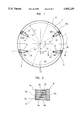
FIGS. 1 and 2 show a first embodiment of a vertical boat according to the present invention. The vertical boat for holding a plurality of wafers 1 comprises two end plates 2 located at the top and the bottom of the boat, and three or more, normally four, support members 5, 6 are mounted vertically between and to the end plates 2. Only the bottom end plate 2 is shown in FIG. 1. Each of the support members 5, 6 is generally a plate whose cross section is a long rectangle. A series of slits 9, 10 for receiving the wafers 1 are formed on each support member 5, 6.
The slits 9, 10 extend over 2/3 or more, preferably 3/4 or more, of the width of the support members 5, 6. By the slits 9, 10 a plurality of arms 100 for supporting the wafers 1 are defined as shown in FIG. 2, which extend horizontally and are parallel to one another. A small support projection 13, 14 is formed at the end of each arm 100 in such a manner that the support projections 13, 14 support the wafer 1 at the inner portions P thereof, whereas the arms 100 extend over the peripheral portion of the wafer in non-contact manner. The inner portions P of the wafer 1 to be supported by the support projections 13, 14 are preferably ranged or spaced from the center 1a of the wafer 1 by 50-90% of the radius of the wafer 1. And the inner portions P of the wafer 1 are preferably arranged in a concentric manner around the center 1a of the wafer 1 as shown in FIGS. 1 and 2.
The peripheral portions of the wafer 1 never contact the support projections 13, 14 of the arms 100 so that the heat does not transfer directly via the peripheral portion of the wafer 1 from the support members 5, 6 to the wafer 1. Also, stress concentration on the peripheral portion of the wafer 1 is decreased.
The height of each support projection 13, 14 is preferably 0.3-3 mm so as to ensure proper gas circulation. The width of each slit 9, 10 is large enough to restrain heat transfer from the boat to the wafers and to prevent gas from stagnating between the wafer and the arm 100.
The vertical boat may be made of silica glass, silicon carbide, carbon, monocrystal silicon, polycrystal silicon, silicon carbide impregnated with silicon and so on, which preferably has a high purity, a large heat resistance and a large corrosion resistance. In the case of silica glass, welding is convenient for connecting the members, while in the other cases they may be assembled in a predetermined manner.
Two types of support members 5, 6 are used in this embodiment, and they are vertically mounted and fixed to the end members 2 parallel to each other.
The support members 5,6 have different lengths and different widths in cross section. Two front support members 5 are located on the wafer inserting side and are formed in the shape of a relatively thin plate. The cross section of the plate 5 has generally a wedge-shape. The slits 9 are formed at predetermined intervals on the support member 5 as shown in FIG. 2. The slits 9 are parallel to each other and extend over approximately 4/5 of the width of the support member 5. A plurality of arms 100 are defined by the slits 9 so that the support member 5 looks like a comb. Each slit 9 has a first slit portion 9a and a second slit portion 9a and a second slit portion 9b as shown in FIG. 2. The first slit portion 9a is longer and wider than the second slit portion 9b. A small support projection 13 is formed at the end of each arm 100. The support projection 13 has relatively a small area, for instance, 12 square millimeters. Two support members 5,5 are positioned so as to face each other.
The other two support members 6, 6 at the rear side are formed in the shape of a thicker plate in comparison with the support member 5. The cross section of the plate 6 has generally a wedge-shape. The slits 10 are formed at predetermined intervals on the support members 6,6 in a similar manner in the support member 5. The slits 10 are parallel to each other and extend over approximately 3/4 of the width of the support member 6. A plurality of arms 100 are defined by the slits 10 so that the support member 6 looks like a comb. The slits 10 are formed in a similar manner in the slit 9. A support projection 14 is also formed at the end of each arm 100. The support projection 14 has relatively a small area, for instance, 12 square millimeters. The support members 6,6 are positioned so as to face the center 1a of the wafer 1.
The wafer 1 is supported by the support members 5,6 in such a manner that the inner portion P of the wafer 1 is supported by the support projections 13,14, whereas the periphery portion of the wafer never contacts the arms 100 of the support member 5,6 and the support projections 13,14.
The slit 9 of the front support member 5 is so formed that the slit bottom 9c is parallel to the wafer inserting direction X. The slits 10 of the rear support member 6 are so formed that the slit bottom 10a thereof is parallel to the tangent line of the circumscribing circle of the wafer 1.
When the wafer 1 is placed properly in the boat, the support projections 9,10 support the wafer not at the peripheral portion thereof but at the inner portion P thereof. The support portion P is preferably concentric around the center 1a of the wafer 1, and spaced from the center 1a of the wafer 1 by 50%-90%, preferably 65%-85%, of the radius of the wafer 1.
The support portions P of the wafer 1 to be supported by the support projections 13,14 are arranged or distributed in a circumferential direction in such a manner that the angle between a line linking the support projection 14 of the rear support member 6 to the center 1a of the wafer 1 and the wafer inserting direction X is 75-180 degrees, preferably 95-140 degrees. The angle defined by a line linking the support projection 13 of the front support member 5 to the center 1a of the wafer 1 and the inserting direction X is 30-120 degrees, preferably 30-80 degrees.
The support projections 13,14 can be arranged in any other manner. For example, the two projections 13,13 of the front support members 9,9 and the two projections 14,14 of the rear support members 10,10 may be positioned so as to be symmetric relative to lines M and N as shown in FIG. 1. The line M passes through the center 1a of the wafer 1 and is parallel to the wafer inserting direction X. The line N passes through the center 1a of the wafer 1 and is perpendicular to the wafer inserting direction X. In this manner the load of the wafer 1 is distributed equally among the four support projections 13,14 so that the wafer 1 can be supported in a good balanced manner. The wafer 1 is placed on the boat in such a manner that the center 1a of the wafer approximately coincides with the center line of the vertical boat.
The support members 5,6 can be produced in the following manner. First, a plate member 5 or 6 is prepared, whose cross section has generally a wedge-shape as shown in FIG. 1. Then a series of first slit portions 9a, of which size is for example 29×5.35 mm, are formed on the plate member 9 or 10 between two sides thereof at a predetermined interval, for example 3 mm, by water jet, for example. A plurality of windows are formed in series along a longitudinal direction of the plate member 5 and side walls 5a,5b are retained. One side wall 5b is, for example, two or three times thicker than the other side wall 5a.
Next, second slit portions 9b are formed on the thin side wall 5a at predetermined intervals, for example 3 mm, by a diamond cutter. The second slit portion 9b has a small width and is connected to the corresponding first slit portion 9b. A series of arms 100 each having a support projection 13 or 14 at the end thereof are defined by the first and the second slit portions 9a,9b. The arms 100 horizontally protrude from the thick side wall 5b so that the thick side wall 5b acts as a support column. The support projection 13 or 14 is, for example, 1 mm in height and has a small top surface for supporting the inner portions P of the wafer 1. Thus comb-shaped support members 9, 10 as shown in FIG. 2 are formed.
After the first slit portions are formed on the plate members, the plate members can be fixed on one or two end members. After that the second slit portions can be formed on the plate members. By this method, the slits can be formed with good accuracy.
After the first slit portions are formed on the plate members, the plates can be impregnated with Si and then the second slits can be formed. In this manner, the second slit portions can be easily machined.
When the slits are formed on the support members in said manner, the slits can be formed with high accuracy because the cut volume is very small in the second step.
FIGS. 3-9 and FIG. 10 show second and third embodiments of the vertical boat according to the present invention, respectively. The vertical boat, in each case, comprises two end plates located on the top and the bottom of the boat, and three or more, normally four, support members 3,4,104 vertically mounted on the end plates. Each support member 3,4,104 has a series of slits 7,8,108 at predetermined intervals along a longitudinal direction thereof. Each support member 3,4,104 is generally a long plate or a long plate-like member.
The slits 7,8,108 extend over 2/3 or more, preferably 3/4 or more, of the width of the support members 3,4,104. By the slits 7,8,108 a series of arms 200 are defined on the support members 3,4,104. Each arm 200 has support projections 11,12,112 at the end thereof in such a manner that the support projections 11,12,112 support the inner portion P of the wafer 1, while the arms 200 extend over the periphery of the wafer in non-contact manner. Said inner portion P of the wafer 1 to be supported by the support projections 11,12,112 is preferably concentric about the center 1a of the wafer 1, and preferably spaced or arranged from the center 1a of the wafer 1 by 50%-90% of the radius of the wafer 1.
In the second embodiment each support member 3,4 has an arc or circular arc cross section. The cross section of the support member can be in an L-shape, a J-shape, a boomerang-shape or other curved-shape. The support members 3,4 can be formed by longitudinally cut pipe. The support member 104 is generally a pipe in the third embodiment. The thickness of each support member 3,4 104 is constant over its full length, but it can be decreased gradually toward their ends. The support members can be modified in various forms, and the structure of the support members is not restricted to the illustrated embodiments.
The peripheral portions of the wafer never contact the support projections 11,12,112 of the support members 3,4,104 so that heat does not transfer via the peripheral portions from the support members to the wafers. The weight concentration on the peripheral portion of the wafer is decreased.
The height of each support projection 11,12,112 can be selected such that the periphery of the wafer does not contact the arms 200 of the support members 3,4,104. It is preferably 0.3-3 mm for ensuring proper gas circulation. The slits have a relatively large size so that the heat transfer from the boat to the wafer is restrained and gas is prevented from stagnating between the wafer and the arms.
The support projections 11,12,112 are preferably positioned in such a manner that the load of the wafer 1 is equally distributed among all the support members 3,4, 104 and the deflection of each wafer 1 is considerably decreased.
Further the second and third embodiments will be explained hereinafter.
In the second embodiment shown in FIGS. 3-9 the vertical boat has two kinds of support members 3,4. The support members 3,4 are generally semi-circular arc plates having different radii of curvature. Two front support members 3,3 are located near the wafer inserting side and faces each other. The radius of curvature of the support member 3 is larger than that of the support member 4. The support member 3 has a plurality of slits 7 at an interval D1 as shown in FIGS. 4 and 5. The slits 7 extend over about 5/6 of the width of the support member 3. A plurality of arms 200 are defined by the slits 7. Each arm 200 has at its end a small support projection 11. The support projection 11 has at its top a small support surface, the area of which is for example 10-150 square millimeters. The support projection 11 is formed so as to support the inner portion P of the wafer 1, whereas the other portions of the arm 200 do not contact the periphery of the wafer 1.
Other support members 4,4 are located on the rear side and have relatively small radii of curvature. The support member 4 has a plurality of slits 8 at a predetermined interval D2 as shown in FIGS. 6 and 7. The slits 8 extend over about 4/5 of the width of the support member 4. A plurality of arms 200 are defined by the slits 8. Each arm 200 has at its end a small support projection 12. The support projection 12 has at its top a small support surface, the area of which is for example 10-50 square millimeters. The support projection 12 is formed so as to support the inner portion P of the wafer 1, whereas the other portions of the arms 200 do not contact the periphery of the wafer 1.
The slit 7 is formed by a first long slit portion 7a with relatively a large width and a second short slit portion 7b with relatively a small width. The slit 8 is also formed by a first long slit portion 8a with relatively a large width and a second short slit portion 8b with relatively a small width.
The inner portion P of the wafer 1 to be supported by the support projections 11,12 is preferably located concentric about the center 1a of the wafer 1, and is preferably arranged or spaced from the center 1a of the wafer 1 by 50-90%, more preferably 65-85%, of the radius of the wafer 1. Therefore the periphery portion of the wafer 1 is not supported by the support projections 11,12.
The support projections 11,12 are preferably distributed in a circumferential direction in such a manner that the angle A between the wafer inserting direction X and a line linking the support projection 12 of the rear support member 4 to the center 1a of the wafer 1 is 75-180 degrees, more preferably 95-140 degrees. On the other hand the angle B between the wafer inserting direction X and a line linking the support projection 11 of the front support member 3 to the center 1a of the wafer 1 is preferably 30-120 degrees, more preferably 30-80 degrees.
The support projections 11,12 can be distributed in any other manner. For example, the two projections 11,11 of the front support members 3,3 and the two projections 12,12 of the rear support members 4,4 can be symmetrical with respect to the line M and the line N shown in FIG. 3. The line M passes through the center 1a of the wafer 1 and is parallel to the wafer inserting direction X, while the line N passes through the center 1a of the wafer 1 and is perpendicular to the wafer inserting direction X. In this manner the load of the wafer 1 is distributed equally among four support projections 11,12 whereby the wafer 1 can be supported in a good balanced manner.
The support member 3 of the second embodiment shown in FIGS. 3-9 can be produced in the following manner. First a pipe member having a relatively large diameter is vertically cut so as to provide a long plate member having a cross section in the shape of an approximately quarter-circular arc. The pipe member has, for example, an outer radius R1 of 40 mm and an inner radius R2 of 34 mm. The long plate member extends circumferentially over, for example, 100 degrees around the center 01 in cross section.
Next a series of first slit portions 7a are formed at the interval D1, for example 12.7 mm, on the plate member. The first slit portions 7a have a width of W1, for example 7 mm, and extend circumferentially over 60-80 degrees around the center 01, which corresponds to the length L1 in FIG. 4. The length L1 is for example 30 mm. The first slit portion can be formed by a laser beam machine, a high pressure jet, a milling cutter, a lather, a diamond cutter and so on. Both longitudinal side walls 3b,3c are retained as shown in FIGS. 6A and 6B. The side wall 3c is thicker than the other side wall 3b so as to act as a column. The thinner wall 3b extends circumferentially over several degrees around the center 01.
Further, a series of second slit portions 7b are formed on the side wall 3b by a diamond cutter. The second slit 7b has a width W2 of 3.2 mm, for example. The second slit portion 7b is cut from the outer surface 3b so as to be connected to the corresponding first slit portion 7a. A series of arms 200 each having a support projection 11 at the end thereof are defined by the first slit portions 7a and the second slit portions 7b as shown in FIGS. 7A and 7B. The support projection 11 has a height of H, for example 1.9 mm, and has a small support surface.
The other support member 4 in FIGS. 3-9 can be produced in the following manner. First a pipe member having a relatively small diameter is vertically cut so as to provide a long plate member having a cross section of a semi-circular arc. For example, the pipe member has an outer radius R3 of 17.5 mm and an inner radius R4 of 10 mm. And the long plate member extends circumferentially over, for example, 225 degrees around the center 02 in cross section.
Next a series of first slit portions 8a are formed at the interval D2, for example 12.7 mm, corresponding to the interval D1 of the slit 7 on the plate member 3. The first slit portions 8a have a width of W3, for example 7 mm, and extends circumferentially over 180 degrees around the center 01. The first slit portion can be formed by a laser beam machine, a high pressure jet, a milling cutter, a lather, a diamond cutter and so on. Both vertical side walls 4b,4c are retained as shown in FIGS. 8A and 8B. The side wall 4c is thicker than the other side wall 4b so as to act as a column. The thin wall 4b extends circumferentially over 20 degrees around the center 02, while the thick wall 4c extends over 40 degrees.
A series of second slit portions 8b are formed at intervals D2, for example 12.7 mm, on the side wall 4b by a diamond cutter. The second slit portion 8b has for instance a width W4 of 3.2 mm. The second slit portion 8b is cut from the outer surface 4a so as to be connected to the corresponding first slit portion 8a. A series of arms 200 each having a support projection 12 at the end thereof are defined by the first slit portions 8a and the second slit portions 8b as shown in FIGS. 9A and 9B. The support projection 12 has, for example a height of 1.9 mm, and a width W5 of 3 mm.
Four support members 3,4 and the slits 7,8 are symmetrical with respect to the plane including the central axis of the boat and parallel to the wafer inserting direction X. However they can be positioned in other manners.
FIG. 10 shows the third embodiment of the present invention. Four pipe-shaped support members 104 are vertically mounted on two end members 2 located at the top and the bottom of the vertical boat. Two front support members 104 are located on the wafer inserting side and have a relatively large diameter for forming a space large enough to insert and to take out the wafers, whereas two rear support members 104 are located on the rear side and have a relatively small diameter for realizing a light-weight construction. However all support members 104 can have the same diameter. On the other hand, the thickness of the support members can be varied by taking into account mechanical strength. In any case section modulus of the support member 104 is preferably 0.3-3.0 cubic centimeter, more preferably 0.52.5 cubic centimeter.
The support members 104 have a series of slits 108 formed at the same interval. The slit 108 can be formed in the following manner. First two series of first slit portions are formed at the same interval from both sides on the pipe member 5. The first slit portion extends over 2/3 and 3/4 of the diameter of the pipe member 5 in the front and the rear support members, respectively. Two side walls are retained.
Next a series of second slit portions are formed on one of the walls at the same interval as the first slit portions by a diamond cutter. Each second slit portion is connected to the corresponding first slit portion. The second slit portion has a smaller width than the first slit portion. The second slit portion has a width of 3.2 mm, for example. A series of arms 200 each having a support projection 112 formed at the end portion near the central axis of the vertical boat are defined by the first and second slit portions.
The support projection 112 has a small support surface formed at the top thereof. It has the area of for example 5-50 square millimeters. The wafer is supported in such a manner that the inner portion of the wafer is supported by the support projections 112 whereas the periphery of the wafer does not contact the arms defined by the slits 108. The inner portion of the wafer is preferably positioned about the center 1a of the wafer 1 and arranged or spaced from the center 1a by 50-90% of the radius of the wafer so that the periphery of the wafer is not supported by the support projections 112 of the arms.
The circumferential positioning manner of the support projections 112 is the same as that of the support projections 11,12 of the second embodiment.
In producing the support members 3,4,104, after the first slit portions are formed on the plate-like members, all plate members can be fixed on one of or both of the end members and then the second slit portions can be formed on the plate-like members. In this method, the slits can be formed with good accuracy.
On the other hand after the first slit portions are formed on the plate-like members, the plate-like members can be impregnated with Si and then the second slits can be formed. In this manner, the second slit portions can be easily machined.
EXAMPLE
A vertical boat for 8-inch wafers was formed from monocrystal silicon. The boat had the same construction as the boat shown in FIGS. 3-9. Also, a conventional vertical boat having four support members was prepared for comparative tests.
A value of deflection of the wafer was calculated by a computer-assisted simulation and actual values were detected by a laser micrometer in cases of the boat of this invention and the conventional boat, respectively. The test results are shown in Table 1. As shown in Table 1, the wafer held on the conventional boat was deflected by 30 microns or more, whereas the wafer held on the boat of the invention was deflected by 5 microns or less. Thus in the invention, the deflection of the wafer was much smaller than that in the prior art.
Next values of curvature during a heat treatment were detected. The results are shown in Table 2. The heat treatment was an oxidation process at the temperature of 1000 degrees celsius for 100 hours. Values of curvature were detected by a laser micrometer.
Also, the number of the slips and the length thereof caused during heat treatments (1)-(3) were detected. The results are shown in Table 3. The heat treatments (1)-(3) were carried out according to Table 4.
As shown in Tables 2,3, in case of the invention, the curvature was smaller than that in the prior art. In this invention, slips rarely occurred.
Thus, by using a vertical boat according to the present invention, deflection and curvature of the wafer was decreased, and slip was effectively inhibited during heat treatments. It is mainly because the inner portions of the wafer were supported by the support projections of the arms whereas the periphery portion of the wafer did not contact the arms of the support members.
              TABLE 1                                                     
______________________________________                                    
                         the present                                      
             the prior art                                                
                         invention                                        
______________________________________                                    
computer-assisted                                                         
               30-180 microns                                             
                             5 microns                                    
simulation                                                                
laser micrometer                                                          
               150 microns   less than 5                                  
                             microns                                      
______________________________________                                    
              TABLE 2                                                     
______________________________________                                    
the prior art     the present invention                                   
______________________________________                                    
500 microns       less than 5 microns                                     
______________________________________                                    
              TABLE 3                                                     
______________________________________                                    
         number of                                                        
                 number of wafers                                         
                              length of the                               
         wafers  having slips slip                                        
______________________________________                                    
heat treatment (1)                                                        
           70        0            --                                      
           (70)      (70)         (10)                                    
heat treatment (2)                                                        
           70        0            --                                      
           (70)      (20)         (5)                                     
heat treatment (3)                                                        
           70        0            --                                      
           (70)       (6)         (1)                                     
______________________________________                                    
 () designates the prior.                                                 
              TABLE 4                                                     
______________________________________                                    
heat treatment (1)                                                        
           insert→800° C.→1000° C.→1100
           ° C.                                                    
(rate: degree/min)    10    6                                             
         →1250° C.→1100° C.→800°
          C.                                                              
         3         3    5                                                 
                                   →discharge                      
heat treatment (2)                                                        
           insert→800° C.→1000° C.→1100
           ° C.                                                    
(rate: degree/min)                                                        
                  10    3                                                 
         →1250° C.→1100° C.→800°
          C.                                                              
         2         2    3                                                 
                                   →discharge                      
heat treatment (3)                                                        
           insert→800° C.→1000° C.→1100
           ° C.                                                    
(rate: degree/min)                                                        
                   5    2                                                 
         →1250° C.→1100° C.→800°
          C.                                                              
         1         1    3                                                 
                                   →discharge                      
______________________________________                                    
 *The heat treatment was performed with an atmosphere of N.sub.2 + O.sub.2

Claims (18)

What is claimed is:
1. A vertical boat for supporting a plurality of semiconductor wafers, each wafer having a peripheral portion and an inner portion therearound, the boat having a top portion and a bottom portion, comprising:
two end members p1aced at the top portion and the bottom portion of the vertical boat; and
a plurality of support members vertically extending between the end members for supporting the wafers,
each of the support members being a plate-like member having a series of slits formed at a predetermined interval thereon,
a plurality of support arms being defined by the slits, the support arms having support projections in such a manner that the inner portion of the wafer contacts and is supported by the support projections whereas the peripheral portion of the wafer does not contact the support projections and the arms of the support members wherein
the inner portion of the wafer to be supported by the support projections ranges from a center of the wafer by 50%-90% of the radius of the wafer,
the vertical boat is made of a material selected from a group consisting of silica glass, silicon carbide, carbon, monocrystal silicon, polycrystal silicon, and silicon carbide impregnated with silicon, and
the support arms and the support projections of the support members are integral with each other so as to constitute a monoblock body.
2. A vertical boat according to claim 1, wherein the inner portion of the wafer to be supported by the support projections ranges from a center of the wafer by 65%-85% of the radius of the wafer.
3. A vertical boat according to c1aim 1, wherein the inner portion of the wafer to be supported by the support projections is positioned about a center of the wafer.
4. A vertical boat according to c1aim 1, wherein the slits extend over 2/3 or more of the width of the plate-like member.
5. A vertical boat according to claim 1, wherein the slits extend over 3/4 or more of the width of the plate-like member.
6. A vertical boat according to claim 1, wherein the slits extend over 4/5 or more of the width of the plate-like member.
7. A vertical boat according to claim 1, wherein the support members include two front support members and two rear support members, the four support members being symmetrical with respect to a plane including a central axis of the vertical boat and parallel to a wafer inserting direction.
8. A vertical boat according to claim 7, wherein the inner portion of the wafer to be supported by the support projections is arranged in a circumferential direction in such a manner that an angle formed by the wafer inserting direction and a line linking the support projection of the rear support member to the center of the wafer is 75-180 degrees, and that an angle formed by the wafer inserting direction and a line linking the support projection of the front support member to a center of the wafer is 30-120 degrees.
9. A vertical boat according to claim 7, wherein the inner portion of the wafer to be supported by the support projections is arranged in a circumferential direction in such a manner that an angle formed between the wafer inserting direction and a line linking the support projection of the rear support member to the center of the wafer is 95-140 degrees, and that an angle formed between the wafer inserting direction and a line linking the support projection of the front support member to a center of the wafer is 30-80 degrees.
10. A vertical boat according to claim 7, wherein the inner portion of the wafer to be supported by the support projections is symmetrical with respect to a plane including a central axis of the vertical boat and perpendicular to a wafer inserting direction.
11. A vertical boat according to claim 1, wherein a section modulus of the support member is 0.3-3.0 cubic centimeters.
12. A vertical boat according to claim 11, wherein a section modulus of the support member is 0.5-2.5 cubic centimeters.
13. A method for producing a vertical boat according to claim 1 comprising the steps of:
forming a series of first slit portions on a plate-like member at a predetermined interval along a longitudinal direction thereof so that two side walls of the plate-like member remain; and
forming a series of second small slit portions on one of the side walls at the same interval so as to connect each second slit portion to the corresponding first slit portion.
14. A method according to claim 13, wherein the second slit portions are formed by a diamond cutter.
15. A method according to claim 13, wherein after said forming of the first slit portions, the plate-like members are mounted on one or two end members, and the second slit portions are formed thereafter.
16. A method according to claim 13, wherein after said forming of the first slit portions, the plate-like members are impregnated with Si, and the second slit portions are formed thereafter.
17. A vertical boat for supporting a plurality of semiconductor wafers, each wafer having a peripheral portion and an inner portion therearound, the boat having a top portion and a bottom portion, comprising:
two end members placed at the top portion and the bottom portion of the vertical boat; and
a plurality of support members vertically extending between the end members for supporting the wafers,
each of the support members being a plate-like member having a series of slits integrally formed at a predetermined interval thereon,
a plurality of support arms being defined by the slits, the support arms having support projections in such a manner that the inner portion of the wafer contacts and is supported by the support projections whereas the peripheral portion of the wafer does not contact the support projections and the arms of the support members.
18. A vertical boat according to claim 17, wherein
the inner portion of the wafer to be supported by the support projections ranges from a center of the wafer by 50%-90% of the radius of the wafer,
the vertical boat is made of a material selected from a group consisting of silica g1ass, silicon carbide, carbon, monocrystal silicon, polycrystal silicon, and silicon carbide impregnated with silicon, and
the support arms and the support projections of the support members are integral with each other so as to constitute a monoblock body.
US08/151,386 1992-11-27 1993-11-12 Vertical boat and a method for making the same Expired - Lifetime US5492229A (en)

Applications Claiming Priority (4)

Application Number Priority Date Filing Date Title
JP33955392A JP3280437B2 (en) 1992-11-27 1992-11-27 Vertical boat
JP4-339553 1992-11-27
JP4-341060 1992-11-30
JP34106092A JP3332168B2 (en) 1992-11-30 1992-11-30 Vertical boat and manufacturing method thereof

Publications (1)

Publication Number Publication Date
US5492229A true US5492229A (en) 1996-02-20

Family

ID=26576449

Family Applications (1)

Application Number Title Priority Date Filing Date
US08/151,386 Expired - Lifetime US5492229A (en) 1992-11-27 1993-11-12 Vertical boat and a method for making the same

Country Status (4)

Country Link
US (1) US5492229A (en)
KR (1) KR0129656B1 (en)
DE (1) DE4340288C2 (en)
GB (1) GB2272964B (en)

Cited By (53)

* Cited by examiner, † Cited by third party
Publication number Priority date Publication date Assignee Title
WO1996035228A1 (en) * 1995-05-05 1996-11-07 Saint-Gobain Industrial Ceramics, Inc. Slip free vertical rack design
US5584401A (en) * 1994-07-29 1996-12-17 Yodogawa Kasei Kabushiki Kaisha Substrate-supporting side boards and a cassette utilizing the boards
US5669513A (en) * 1995-09-25 1997-09-23 Samsung Electronics Co., Ltd. Wafer carriage
FR2750963A1 (en) * 1996-07-12 1998-01-16 Fluoroware Inc CONTAINER FOR SLICES, IN PARTICULAR SEMICONDUCTORS
US5718574A (en) * 1995-03-01 1998-02-17 Tokyo Electron Limited Heat treatment apparatus
US5752609A (en) * 1996-02-06 1998-05-19 Tokyo Electron Limited Wafer boat
US5779797A (en) * 1995-11-15 1998-07-14 Nec Corporation Wafer boat for vertical diffusion and vapor growth furnace
US5841515A (en) * 1995-09-27 1998-11-24 Dainippon Screen Mfg. Co., Ltd. Substrate container cassette, interface mechanism, and substrate processing
US5858103A (en) * 1996-05-17 1999-01-12 Asahi Glass Company Ltd. Vertical wafer boat
US5890598A (en) * 1997-01-22 1999-04-06 Nec Corporation Substrate cassette
US5931666A (en) * 1998-02-27 1999-08-03 Saint-Gobain Industrial Ceramics, Inc. Slip free vertical rack design having rounded horizontal arms
WO1999050606A1 (en) * 1998-04-01 1999-10-07 Applied Materials, Inc. Substrate support for a thermal processing chamber
US6074479A (en) * 1996-06-28 2000-06-13 Sumitomo Metal Industries Ltd. Silicon single crystal wafer annealing method and equipment, and silicon single crystal wafer and manufacturing method related thereto
US6099645A (en) * 1999-07-09 2000-08-08 Union Oil Company Of California Vertical semiconductor wafer carrier with slats
WO2000063952A1 (en) * 1999-04-15 2000-10-26 Integrated Materials, Inc. Silicon fixtures for wafer processing and method of fabrication
US6171400B1 (en) 1998-10-02 2001-01-09 Union Oil Company Of California Vertical semiconductor wafer carrier
US6196211B1 (en) * 1999-04-15 2001-03-06 Integrated Materials, Inc. Support members for wafer processing fixtures
US6205993B1 (en) 1999-04-15 2001-03-27 Integrated Materials, Inc. Method and apparatus for fabricating elongate crystalline members
US6225594B1 (en) * 1999-04-15 2001-05-01 Integrated Materials, Inc. Method and apparatus for securing components of wafer processing fixtures
US6340090B1 (en) * 1999-01-07 2002-01-22 Tooltek Engineering Corporation Substrate fixturing device
WO2002003428A3 (en) * 2000-06-30 2002-04-11 Integrated Materials Inc Silicon fixtures for supporting wafers during thermal processing and method of fabrication
US20020119641A1 (en) * 2001-02-26 2002-08-29 Zehavi Raanan Y. High temperature hydrogen anneal of silicon wafers supported on a silicon fixture
US6450346B1 (en) 2000-06-30 2002-09-17 Integrated Materials, Inc. Silicon fixtures for supporting wafers during thermal processing
US6455395B1 (en) 2000-06-30 2002-09-24 Integrated Materials, Inc. Method of fabricating silicon structures including fixtures for supporting wafers
US6488497B1 (en) * 2001-07-12 2002-12-03 Saint-Gobain Ceramics & Plastics, Inc. Wafer boat with arcuate wafer support arms
US6497403B2 (en) 2000-12-28 2002-12-24 Memc Electronic Materials, Inc. Semiconductor wafer holder
GB2330944B (en) * 1997-10-20 2003-01-22 Fluoroware Inc Wafer carrier with minimal contact
US6576064B2 (en) 1997-07-10 2003-06-10 Sandia Corporation Support apparatus for semiconductor wafer processing
US6582221B1 (en) 2002-07-19 2003-06-24 Asm International N.V. Wafer boat and method for treatment of substrates
US20030180125A1 (en) * 2002-03-15 2003-09-25 Van Den Berg Jannes Remco Method and apparatus for batch processing of wafers in a furnace
US20040040632A1 (en) * 2002-08-30 2004-03-04 Oosterlaken Theodorus Gerardus Maria Susceptor plate for high temperature heat treatment
US6776289B1 (en) 1996-07-12 2004-08-17 Entegris, Inc. Wafer container with minimal contact
US6799940B2 (en) 2002-12-05 2004-10-05 Tokyo Electron Limited Removable semiconductor wafer susceptor
US20040197174A1 (en) * 2003-04-02 2004-10-07 Van Den Berg Jannes Remco Method and apparatus for loading a batch of wafers into a wafer boat
US20050023231A1 (en) * 2003-08-01 2005-02-03 Chui-Kai Huang Substrate supporting rod and substrate cassette using the same
US20050205502A1 (en) * 2004-03-18 2005-09-22 Brown Steven A Rails for semiconductor wafer carriers
US20060060145A1 (en) * 2004-09-17 2006-03-23 Van Den Berg Jannes R Susceptor with surface roughness for high temperature substrate processing
US20060065634A1 (en) * 2004-09-17 2006-03-30 Van Den Berg Jannes R Low temperature susceptor cleaning
US20060113806A1 (en) * 2004-11-29 2006-06-01 Asm Japan K.K. Wafer transfer mechanism
US20060150906A1 (en) * 2005-01-07 2006-07-13 Selen Louis J M Wafer boat for reduced shadow marks
US20060208434A1 (en) * 2003-03-31 2006-09-21 Sumco Corporation Silicon wafer heat treatment jig, and silicon wafer heat treatment method
US20070020885A1 (en) * 2001-05-18 2007-01-25 Integrated Materials, Inc. Tube Formed of Bonded Silicon Staves
US7181132B2 (en) 2003-08-20 2007-02-20 Asm International N.V. Method and system for loading substrate supports into a substrate holder
US20100200962A1 (en) * 2006-10-16 2010-08-12 Takayuki Kihara Silocon wafer supporting method, heat treatment jig and heat-treated wafer
US20110309562A1 (en) * 2010-06-18 2011-12-22 Tokyo Electron Limited Support structure and processing apparatus
US20120125808A1 (en) * 2005-07-08 2012-05-24 Bonora Anthony C Workpiece support structures and apparatus for accessing same
US20120240857A1 (en) * 2010-09-29 2012-09-27 Tokyo Electron Limited Vertical heat treatment apparatus
US20140302447A1 (en) * 2013-04-09 2014-10-09 Asm Ip Holding B.V. Wafer boat having dual pitch
US20170110353A1 (en) * 2015-10-20 2017-04-20 Taiwan Semiconductor Manufacturing Co., Ltd. Wafer boat, annealing tool and annealing method
US20170287758A1 (en) * 2014-09-26 2017-10-05 Miraial Co., Ltd Substrate storing container
TWI609749B (en) * 2014-05-16 2018-01-01 Nidec Sankyo Corp Industrial robot hand and industrial robot
US20180019144A1 (en) * 2016-07-15 2018-01-18 Coorstek Kk Vertical wafer boat
US10008402B1 (en) * 2017-02-21 2018-06-26 Coorstek Kk Vertical wafer boat

Families Citing this family (3)

* Cited by examiner, † Cited by third party
Publication number Priority date Publication date Assignee Title
JP3280438B2 (en) * 1992-11-30 2002-05-13 東芝セラミックス株式会社 Vertical boat
GB2348634B (en) * 1996-07-12 2000-12-06 Fluoroware Inc Wafer carrier
NL1010321C2 (en) * 1997-10-20 1999-09-08 Fluoroware Inc Wafer carrier.

Citations (6)

* Cited by examiner, † Cited by third party
Publication number Priority date Publication date Assignee Title
US4153164A (en) * 1978-06-13 1979-05-08 Kasper Instruments, Inc. Carrier for semiconductive wafers
US4407654A (en) * 1982-01-21 1983-10-04 The Potters Supply Company Handling and support system for kiln fired ware
US4412812A (en) * 1981-12-28 1983-11-01 Mostek Corporation Vertical semiconductor furnace
JPS62128633A (en) * 1985-11-29 1987-06-10 Fujitsu Ltd Generating circuit for staff synchronizing clock
WO1992006342A1 (en) * 1990-10-09 1992-04-16 Groom Bryan Ltd Ware support apparatus
US5219079A (en) * 1991-10-11 1993-06-15 Rohm Co., Ltd. Wafer jig

Family Cites Families (2)

* Cited by examiner, † Cited by third party
Publication number Priority date Publication date Assignee Title
JPS60107843A (en) * 1983-11-16 1985-06-13 Tekunisuko:Kk Assembly type supporter
JPH0715138Y2 (en) * 1986-02-07 1995-04-10 信越石英株式会社 Vertical storage jig

Patent Citations (6)

* Cited by examiner, † Cited by third party
Publication number Priority date Publication date Assignee Title
US4153164A (en) * 1978-06-13 1979-05-08 Kasper Instruments, Inc. Carrier for semiconductive wafers
US4412812A (en) * 1981-12-28 1983-11-01 Mostek Corporation Vertical semiconductor furnace
US4407654A (en) * 1982-01-21 1983-10-04 The Potters Supply Company Handling and support system for kiln fired ware
JPS62128633A (en) * 1985-11-29 1987-06-10 Fujitsu Ltd Generating circuit for staff synchronizing clock
WO1992006342A1 (en) * 1990-10-09 1992-04-16 Groom Bryan Ltd Ware support apparatus
US5219079A (en) * 1991-10-11 1993-06-15 Rohm Co., Ltd. Wafer jig

Cited By (82)

* Cited by examiner, † Cited by third party
Publication number Priority date Publication date Assignee Title
US5584401A (en) * 1994-07-29 1996-12-17 Yodogawa Kasei Kabushiki Kaisha Substrate-supporting side boards and a cassette utilizing the boards
US5718574A (en) * 1995-03-01 1998-02-17 Tokyo Electron Limited Heat treatment apparatus
US5865321A (en) * 1995-05-05 1999-02-02 Saint-Gobain/Norton Industrial Ceramics Corp. Slip free vertical rack design
WO1996035228A1 (en) * 1995-05-05 1996-11-07 Saint-Gobain Industrial Ceramics, Inc. Slip free vertical rack design
US5669513A (en) * 1995-09-25 1997-09-23 Samsung Electronics Co., Ltd. Wafer carriage
US5841515A (en) * 1995-09-27 1998-11-24 Dainippon Screen Mfg. Co., Ltd. Substrate container cassette, interface mechanism, and substrate processing
US5779797A (en) * 1995-11-15 1998-07-14 Nec Corporation Wafer boat for vertical diffusion and vapor growth furnace
US5752609A (en) * 1996-02-06 1998-05-19 Tokyo Electron Limited Wafer boat
US5858103A (en) * 1996-05-17 1999-01-12 Asahi Glass Company Ltd. Vertical wafer boat
US6074479A (en) * 1996-06-28 2000-06-13 Sumitomo Metal Industries Ltd. Silicon single crystal wafer annealing method and equipment, and silicon single crystal wafer and manufacturing method related thereto
FR2750963A1 (en) * 1996-07-12 1998-01-16 Fluoroware Inc CONTAINER FOR SLICES, IN PARTICULAR SEMICONDUCTORS
US6776289B1 (en) 1996-07-12 2004-08-17 Entegris, Inc. Wafer container with minimal contact
US5890598A (en) * 1997-01-22 1999-04-06 Nec Corporation Substrate cassette
US6576064B2 (en) 1997-07-10 2003-06-10 Sandia Corporation Support apparatus for semiconductor wafer processing
GB2330944B (en) * 1997-10-20 2003-01-22 Fluoroware Inc Wafer carrier with minimal contact
US5931666A (en) * 1998-02-27 1999-08-03 Saint-Gobain Industrial Ceramics, Inc. Slip free vertical rack design having rounded horizontal arms
WO1999050606A1 (en) * 1998-04-01 1999-10-07 Applied Materials, Inc. Substrate support for a thermal processing chamber
US6280183B1 (en) * 1998-04-01 2001-08-28 Applied Materials, Inc. Substrate support for a thermal processing chamber
US6532642B1 (en) 1998-10-02 2003-03-18 Union Oil Company Of California Method of making a silicon carbide rail for use in a semiconductor wafer carrier
US6171400B1 (en) 1998-10-02 2001-01-09 Union Oil Company Of California Vertical semiconductor wafer carrier
US6357604B1 (en) 1998-10-02 2002-03-19 Larry S. Wingo Long tooth rails for semiconductor wafer carriers
US6340090B1 (en) * 1999-01-07 2002-01-22 Tooltek Engineering Corporation Substrate fixturing device
US6225594B1 (en) * 1999-04-15 2001-05-01 Integrated Materials, Inc. Method and apparatus for securing components of wafer processing fixtures
US6357432B2 (en) 1999-04-15 2002-03-19 Integrated Materials, Inc. Silicon support members for wafer processing fixtures
US6205993B1 (en) 1999-04-15 2001-03-27 Integrated Materials, Inc. Method and apparatus for fabricating elongate crystalline members
US6196211B1 (en) * 1999-04-15 2001-03-06 Integrated Materials, Inc. Support members for wafer processing fixtures
US6617540B2 (en) 1999-04-15 2003-09-09 Integrated Materials, Inc. Wafer support fixture composed of silicon
WO2000063952A1 (en) * 1999-04-15 2000-10-26 Integrated Materials, Inc. Silicon fixtures for wafer processing and method of fabrication
US6099645A (en) * 1999-07-09 2000-08-08 Union Oil Company Of California Vertical semiconductor wafer carrier with slats
US20040040885A1 (en) * 2000-06-30 2004-03-04 Boyle James E. Silicon wafer tower with inclined support teeth
US6617225B2 (en) * 2000-06-30 2003-09-09 Integrated Materials, Inc. Method of machining silicon
EP1297558B1 (en) * 2000-06-30 2011-04-20 Integrated Materials, Inc. Silicon fixtures for supporting wafers during thermal processing and method of fabrication
US6455395B1 (en) 2000-06-30 2002-09-24 Integrated Materials, Inc. Method of fabricating silicon structures including fixtures for supporting wafers
WO2002003428A3 (en) * 2000-06-30 2002-04-11 Integrated Materials Inc Silicon fixtures for supporting wafers during thermal processing and method of fabrication
US6450346B1 (en) 2000-06-30 2002-09-17 Integrated Materials, Inc. Silicon fixtures for supporting wafers during thermal processing
US6497403B2 (en) 2000-12-28 2002-12-24 Memc Electronic Materials, Inc. Semiconductor wafer holder
US6727191B2 (en) * 2001-02-26 2004-04-27 Integrated Materials, Inc. High temperature hydrogen anneal of silicon wafers supported on a silicon fixture
US20040197974A1 (en) * 2001-02-26 2004-10-07 Zehavi Raanan Y Silicon fixture supporting silicon wafers during high temperature processing
US6979659B2 (en) 2001-02-26 2005-12-27 Integrated Materials, Inc. Silicon fixture supporting silicon wafers during high temperature processing
US20020119641A1 (en) * 2001-02-26 2002-08-29 Zehavi Raanan Y. High temperature hydrogen anneal of silicon wafers supported on a silicon fixture
US7854974B2 (en) * 2001-05-18 2010-12-21 Integrated Materials, Inc. Tube formed of bonded silicon staves
US20070020885A1 (en) * 2001-05-18 2007-01-25 Integrated Materials, Inc. Tube Formed of Bonded Silicon Staves
WO2003007336A3 (en) * 2001-07-12 2003-07-03 Saint Gobain Ceramics Wafer boat with arcuate wafer support arms
US6488497B1 (en) * 2001-07-12 2002-12-03 Saint-Gobain Ceramics & Plastics, Inc. Wafer boat with arcuate wafer support arms
CN100412489C (en) * 2001-07-12 2008-08-20 圣戈本陶瓷及塑料股份有限公司 Wafer boat with arcuate wafer support arms
US6835039B2 (en) 2002-03-15 2004-12-28 Asm International N.V. Method and apparatus for batch processing of wafers in a furnace
US20030180125A1 (en) * 2002-03-15 2003-09-25 Van Den Berg Jannes Remco Method and apparatus for batch processing of wafers in a furnace
US6582221B1 (en) 2002-07-19 2003-06-24 Asm International N.V. Wafer boat and method for treatment of substrates
US7256375B2 (en) 2002-08-30 2007-08-14 Asm International N.V. Susceptor plate for high temperature heat treatment
US20040040632A1 (en) * 2002-08-30 2004-03-04 Oosterlaken Theodorus Gerardus Maria Susceptor plate for high temperature heat treatment
US6799940B2 (en) 2002-12-05 2004-10-05 Tokyo Electron Limited Removable semiconductor wafer susceptor
US20060208434A1 (en) * 2003-03-31 2006-09-21 Sumco Corporation Silicon wafer heat treatment jig, and silicon wafer heat treatment method
US7481888B2 (en) 2003-03-31 2009-01-27 Sumco Corporation Heat treatment jig and heat treatment method for silicon wafer
US8026182B2 (en) 2003-03-31 2011-09-27 Sumco Corporation Heat treatment jig and heat treatment method for silicon wafer
CN1768421B (en) * 2003-03-31 2010-04-28 株式会社上睦可 Silicon wafer heat treatment jig, and silicon wafer heat treatment method
US20090127746A1 (en) * 2003-03-31 2009-05-21 Sumco Corporation Heat treatment jig and heat treatment method for silicon wafer
US20040197174A1 (en) * 2003-04-02 2004-10-07 Van Den Berg Jannes Remco Method and apparatus for loading a batch of wafers into a wafer boat
US7033126B2 (en) 2003-04-02 2006-04-25 Asm International N.V. Method and apparatus for loading a batch of wafers into a wafer boat
US20050023231A1 (en) * 2003-08-01 2005-02-03 Chui-Kai Huang Substrate supporting rod and substrate cassette using the same
US7334690B2 (en) * 2003-08-01 2008-02-26 Foxsemicon Integrated Technology, Inc. Substrate supporting rod and substrate cassette using the same
US7181132B2 (en) 2003-08-20 2007-02-20 Asm International N.V. Method and system for loading substrate supports into a substrate holder
US7570876B2 (en) 2003-08-20 2009-08-04 Asm International N.V. Method and system for loading substrate supports into a substrate holder
US20050205502A1 (en) * 2004-03-18 2005-09-22 Brown Steven A Rails for semiconductor wafer carriers
WO2005091341A1 (en) * 2004-03-18 2005-09-29 Poco Graphite, Inc. Improved rails for semiconductor wafer carriers
US20060060145A1 (en) * 2004-09-17 2006-03-23 Van Den Berg Jannes R Susceptor with surface roughness for high temperature substrate processing
US20060065634A1 (en) * 2004-09-17 2006-03-30 Van Den Berg Jannes R Low temperature susceptor cleaning
US20060113806A1 (en) * 2004-11-29 2006-06-01 Asm Japan K.K. Wafer transfer mechanism
US20060150906A1 (en) * 2005-01-07 2006-07-13 Selen Louis J M Wafer boat for reduced shadow marks
US20120125808A1 (en) * 2005-07-08 2012-05-24 Bonora Anthony C Workpiece support structures and apparatus for accessing same
US8800774B2 (en) * 2005-07-08 2014-08-12 Brooks Automation, Inc. Workpiece support structures and apparatus for accessing same
US8067820B2 (en) * 2006-10-16 2011-11-29 Sumco Corporation Silocon wafer supporting method, heat treatment jig and heat-treated wafer
US20100200962A1 (en) * 2006-10-16 2010-08-12 Takayuki Kihara Silocon wafer supporting method, heat treatment jig and heat-treated wafer
US20110309562A1 (en) * 2010-06-18 2011-12-22 Tokyo Electron Limited Support structure and processing apparatus
US20120240857A1 (en) * 2010-09-29 2012-09-27 Tokyo Electron Limited Vertical heat treatment apparatus
US20140302447A1 (en) * 2013-04-09 2014-10-09 Asm Ip Holding B.V. Wafer boat having dual pitch
US10008401B2 (en) * 2013-04-09 2018-06-26 Asm Ip Holding B.V. Wafer boat having dual pitch
TWI609749B (en) * 2014-05-16 2018-01-01 Nidec Sankyo Corp Industrial robot hand and industrial robot
US20170287758A1 (en) * 2014-09-26 2017-10-05 Miraial Co., Ltd Substrate storing container
US10535540B2 (en) * 2014-09-26 2020-01-14 Miraial Co., Ltd. Substrate storing container
US20170110353A1 (en) * 2015-10-20 2017-04-20 Taiwan Semiconductor Manufacturing Co., Ltd. Wafer boat, annealing tool and annealing method
US20180019144A1 (en) * 2016-07-15 2018-01-18 Coorstek Kk Vertical wafer boat
US10008402B1 (en) * 2017-02-21 2018-06-26 Coorstek Kk Vertical wafer boat

Also Published As

Publication number Publication date
GB2272964B (en) 1997-02-05
GB9324463D0 (en) 1994-01-12
DE4340288A1 (en) 1994-06-01
DE4340288C2 (en) 1996-10-02
KR0129656B1 (en) 1998-04-06
KR940012571A (en) 1994-06-23
GB2272964A (en) 1994-06-01

Similar Documents

Publication Publication Date Title
US5492229A (en) Vertical boat and a method for making the same
US6357604B1 (en) Long tooth rails for semiconductor wafer carriers
US6099645A (en) Vertical semiconductor wafer carrier with slats
KR100235078B1 (en) Wafer boat for vertical diffusion and vapor growth furnace
JP4467028B2 (en) Vertical wafer support jig
US5931666A (en) Slip free vertical rack design having rounded horizontal arms
US4653636A (en) Wafer carrier and method
US6110285A (en) Vertical wafer boat
US5507873A (en) Vertical boat
JPH10284429A (en) Wafer supporting device
KR100424428B1 (en) Vertical furnace and wafer boat for vertical furnace
JPH09260296A (en) Wafer retainer
CN213184238U (en) Silicon boat with chamfer on edge of groove tooth
JPH06168902A (en) Vertical boat
JP3332168B2 (en) Vertical boat and manufacturing method thereof
KR20010062144A (en) Substrate holder for heat treatment, heat treatment apparatus and method of substrate
JP3507624B2 (en) Heat treatment boat and heat treatment equipment
US5711808A (en) Boat for vertical diffusion furnace
JP2001176811A (en) Wafer support device
JPH05234925A (en) Wafer retaining boat
JPH0117244B2 (en)
JPH1140659A (en) Heat treating vertical boat for semiconductor wafer
JPH0438718B2 (en)
JPH0824140B2 (en) Silicon wafer processing jig
JPH0220830Y2 (en)

Legal Events

Date Code Title Description
AS Assignment

Owner name: TOSHIBA CERAMICS CO., LTD., JAPAN

Free format text: ASSIGNMENT OF ASSIGNORS INTEREST;ASSIGNORS:TANAKA, TAKASHI;YOSHIKAWA, JUN;TOYA, EIICHI;AND OTHERS;REEL/FRAME:006859/0942;SIGNING DATES FROM 19931209 TO 19931221

STCF Information on status: patent grant

Free format text: PATENTED CASE

FPAY Fee payment

Year of fee payment: 4

FEPP Fee payment procedure

Free format text: PAYOR NUMBER ASSIGNED (ORIGINAL EVENT CODE: ASPN); ENTITY STATUS OF PATENT OWNER: LARGE ENTITY

FPAY Fee payment

Year of fee payment: 8

FPAY Fee payment

Year of fee payment: 12

AS Assignment

Owner name: COVALENT MATERIALS CORPORATION, JAPAN

Free format text: MERGER;ASSIGNOR:TOSHIBA CERAMICS CO., LTD.;REEL/FRAME:019817/0749

Effective date: 20070601