US5495594A - Technique for automatically adapting a peripheral integrated circuit for operation with a variety of microprocessor control signal protocols - Google Patents
Technique for automatically adapting a peripheral integrated circuit for operation with a variety of microprocessor control signal protocols Download PDFInfo
- Publication number
- US5495594A US5495594A US08/248,468 US24846894A US5495594A US 5495594 A US5495594 A US 5495594A US 24846894 A US24846894 A US 24846894A US 5495594 A US5495594 A US 5495594A
- Authority
- US
- United States
- Prior art keywords
- signal
- microprocessor
- pin
- state
- storage means
- Prior art date
- Legal status (The legal status is an assumption and is not a legal conclusion. Google has not performed a legal analysis and makes no representation as to the accuracy of the status listed.)
- Expired - Lifetime
Links
Images


Classifications
-
- G—PHYSICS
- G06—COMPUTING; CALCULATING OR COUNTING
- G06F—ELECTRIC DIGITAL DATA PROCESSING
- G06F13/00—Interconnection of, or transfer of information or other signals between, memories, input/output devices or central processing units
- G06F13/38—Information transfer, e.g. on bus
- G06F13/42—Bus transfer protocol, e.g. handshake; Synchronisation
- G06F13/4204—Bus transfer protocol, e.g. handshake; Synchronisation on a parallel bus
- G06F13/4208—Bus transfer protocol, e.g. handshake; Synchronisation on a parallel bus being a system bus, e.g. VME bus, Futurebus, Multibus
- G06F13/4213—Bus transfer protocol, e.g. handshake; Synchronisation on a parallel bus being a system bus, e.g. VME bus, Futurebus, Multibus with asynchronous protocol
Definitions
- This invention relates generally to the recognition and interpretation of the operational and control signals used by a computer system microprocessor, by its peripheral chips, and, more specifically, to providing peripheral chips that operate with several different types of microprocessors having various signaling protocols.
- peripheral circuit chips typically function to provide parallel input-output, serial input-output, interface with system memory, memory management, direct memory access (“DMA”) control, event counting and timing circuits, high speed numerical processing, and various other similar functions that need to be provided along with the MPU in order to form a complete computer system.
- DMA direct memory access
- semiconductor manufacturers designed their own techniques and signal protocols for controlling operation of the peripheral circuits from the microprocessor. Although these techniques had many common aspects, they also had many differences that prevented a peripheral circuit of one semiconductor manufacturer from working with a microprocessor of another, or at least without the addition of translation or "glue” logic between them.
- peripheral circuits Over time, as the number of types of peripheral circuits being provided increased dramatically, along with an increasing number of microprocessor types, it became impossible for any single semiconductor manufacturer to provide a full line of peripherals for all of its own microprocessors. Also, as certain peripheral parts became popular because of better designs and more complete functions, computer system designers began to use peripheral devices of one semiconductor manufacturer family with a microprocessor of another. The trend lately has been for semiconductor manufacturers to design both microprocessors that can be more easily interfaced to an increasing number of peripheral devices, and to also design peripheral devices that can be more easily used with a variety of microprocessors from different manufacturers.
- Each popular microprocessor still has its own particular interfacing requirements, including specific signal protocols, but there is a considerable commonality between them and the differences are now well defined. Examples of such differences include the use by some microprocessors of an 8-bit wide data bus and use by others of a 16-bit wide data bus. In the case of a 16-bit wide data bus, some microprocessors use the least significant address line (A0) to designate which half of the bus is being used to transfer a single byte of data, along with a single data strobe to transfer that byte, while other microprocessors use separate data strobes for transferring bytes on the lower and upper byte data bus lines. Further, microprocessors that so utilize the A0 line do so with different polarities.
- A0 least significant address line
- microprocessors in communicating with peripheral devices is in designating whether data is to be written from the data bus to the peripheral device or read from it.
- separate read and write strobe signals are provided.
- one signal is provided to designate whether a read or write operation is to take place, and another signal acts as a data strobe to implement that operation.
- microprocessors also differ in the polarities used to designate the read-write control signal.
- a peripheral circuit often needs to delay and slow down the operation of the microprocessor to allow the peripheral enough time to capture write data or provide read data asked of it by the microprocessor.
- Typical situations where this occurs is when the peripheral device is unable to provide read data to the microprocessor within the time required to maintain full speed operation of the microprocessor, or when the peripheral device is unable to accept and capture write data provided by the microprocessor quickly enough to allow the microprocessor to move on to its next operation at its full speed.
- Two alternative techniques have emerged for allowing the peripheral device to slow down the microprocessor in such circumstances.
- One method is for the peripheral device to emit a WAIT signal as soon as it recognizes that it is not going to be able to complete its designated task before the microprocessor will want to move on to its next operation.
- An alternative technique is for the peripheral device to emit an acknowledge (ACK) signal when it begins to perform an operation requested of it by the microprocessor and then terminate that signal when the task has been completed.
- ACK acknowledge
- control register having fields whose bits determine which among various signaling protocols is to be used on a group of control signal pins.
- the control register is loaded each time the computer system in which the peripherals are used is initialized or reset. This technique is limited in its flexibility in that the operation of loading the control register is itself accomplished using at least some of the control signals being defined.
- a peripheral device includes several control signal pins that are each connectable to different types of control signals and protocols used by various microprocessors, circuits being provided as part of the device to automatically recognize which signals and protocols are being used by the microprocessor. This is done by monitoring the signals during the first few operations performed by the microprocessor after initialization or reset of the computer system. After this initialization learning process is completed, the recognized one of the various different signals and protocols that can be connected to these pins is automatically converted within the peripheral circuit to a common protocol and set of signals. This protocol and signals are then utilized to control operation of the peripheral device circuitry, including, for example, control of its data bus configuration and transfers of data over it and a designation of the type of speed matching signaling that is to be utilized.
- a plurality of latches are connected through appropriate logic to a number of control signal pins including those which are designed to operate with different signal protocols.
- the state of several of these latches is set upon observing the types of signals used by the microprocessor during its first operations after initialization. Examples of such latches include one for determining whether the data bus is 8 or 16 bits wide, whether the A0 address line is utilized, and which read/write control signal protocol is used.
- the states of another set of latches observing many of the same microprocessor signals are set upon the first access by the microprocessor to the specific peripheral chip, specific constraints being set on the nature of the first access.
- Examples of information stored in this second set of latches is the polarity convention of the A0 signal, if used, and the polarity convention of a read/write signal, if used.
- a logic system receives the outputs of these latches and other incoming control signals to generate internal control signals that have the same protocol for any of the microprocessor signals that may be connected to the multipurpose control signal pins.
- Yet another latch learns whether the wait or acknowledge speed matching protocol is used by the microprocessor, and the information stored there connects either a wait logic circuit or an acknowledge logic circuit to a common pin.
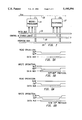
- FIG. 1 shows in very general terms a portion of a computer system having a microprocessor and a peripheral connected to operate together;
- FIG. 2 is a block diagram of the peripheral circuit of FIG. 1;
- FIG. 3 is a circuit diagram of one of the blocks shown in FIG. 2;
- FIG. 4 is a circuit diagram of one of the blocks shown in FIG. 3;
- FIGS. 5(A) and 5(B) provide waveforms to illustrate one existing read-write signaling protocol
- FIGS. 6(A) and 6(B) provide waveforms to illustrate another existing read-write protocol
- FIG. 7 is a set of waveforms that illustrates a wait control signal protocol
- FIG. 8 is a set of waveforms that shows an acknowledge signal protocol
- FIG. 9 is a circuit diagram illustrating another of the blocks of the circuit of FIG. 2.
- a microprocessor integrated circuit device 11 is illustrated to be of a type that utilizes a data bus 13 that is separate from an address bus 15, although the invention can be used with a multiplexed address/data bus by simply capturing the state of address line 0 in a demultiplexing latch, the output of which is then connected to the A0 signal shown in the drawings.
- a peripheral integrated circuit device 17 is shown to be connected to those same busses.
- a number of system control and status lines 19 are also connected to each of the microprocessor 11 and peripheral 17, as is a voltage supply line 21.
- a complete computer system will include a number of additional peripheral integrated circuit devices, memories, timing circuits and the like, not shown in FIG. 1.
- a primary portion 23 of the peripheral circuit performs the functions for which the circuit is utilized, such as a parallel input-output device, serial input-output device, memory interface, and the like. Any such circuit 23 may be connected through a plurality of package pins 25, in this case seven, to the system address bus, designated in this example as A0-A6, or it may be connected to the outputs of a plurality of demultiplexing latches that capture address information.
- circuit portion 23 is connectable to a system data bus which may or may not also carry multiplexed addresses. Since one of the capabilities of a peripheral device using the present invention is to transfer data 16 bits at a time, circuit 23 includes an internal data bus that is 16 bits wide, and is divided into two 8-bit groups INT D15-8 and INT D7-0.
- One set of 8 device pins 27 is provided for connecting to an 8-bit system data bus D7-0 or to 8 lines of a system data bus that includes 16 or more data lines.
- Another set of 8 device pins 29 is provided for connecting to 8 more lines of a system data bus that includes 16 or more data lines. If the device is configured for 8-bit data only, the pins 29 can be used for other functions.
- the data bus pins are connected to the INT D15-8 and INT D7-0 through a plurality of gated directional buffer amplifiers (drivers and receivers).
- An amplifier 31 when gated on by the output of an AND-gate 33, drives the state of the D7-0 pins onto INT D7-0 during a write operation.
- such a buffer 35 drives, in response to the output of an AND-gate 37, the state of INT D7-0 onto the D7-0 pins during a read operation.
- a write buffer 39 gated by an output of an AND-gate 41
- a read buffer 43 gated by an output of an AND-gate 45
- Another set of such buffers 47 and 49 are gated from the outputs of respective AND-gates 51 and 53 for transferring between INT D15-8 and the D7-0 pins, which is required when the external system data bus is only 8 bits wide.
- the primary functional circuit portion 23 will likely have a plurality of lines 55 that are connected to separate pins, a number depending upon the function of the circuit portion 23. For example, if it is a serial input-output device, lines 55 may be connected to another computer system, a printer, or a display terminal. For proper operation, the circuit also requires connection with at least a majority of the control and status lines 19 of the computer system.
- a pin 57 is designated for receiving a RESET* signal from the microprocessor 11.
- a pin 59 is designated for receiving a chip select (CS*) signal from external address-decoding logic. Both of the pins 57 and 59 are connected directly to the main circuit portion 23.
- the asterisk (*) used after the signal names herein is intended to identify those signals that are active when in their low voltage state.)
- at least one pin 61 needs to be provided for a voltage supply V CC ,
- the main functional circuit portion 23 likely requires connection with a number of the other system control and status lines 19 in order to operate, and certainly control signals are required from the microprocessor in order to direct the flow of data over the data bus by appropriately gating the various buffer amplifiers that are provided in the path of the data bus, as described above.
- Three pins 63, 65 and 67 are designated for connecting with three additional of the system control and status lines 19. But each of these three pins is intended to be connected to different control signals depending upon the type of microprocessor 11 with which the peripheral circuit is being used. Therefore, before signals from these pins are utilized within the peripheral circuit, they are passed through circuits indicated by a block 69.
- a primary purpose of the circuits 69 which are described below with respect to FIG.
- circuits 69 are able to recognize various different microprocessor control signals related to transfers of data over the data bus and translate those control signals into a form on lines 73-77 which is the same no matter which of the various microprocessor control signal protocols is being utilized.
- each of the data bus AND-gates 33, 37, 51, 53, 41 and 45 receive as an input a chip select (CS) signal in a line 79, a result of an inverter 81 receiving the CS* signal from the pin 59. This then limits any data transactions on the data bus to occur only when the microprocessor addresses this particular circuit for operation.
- the chip select signal (CS*) is received at pin 59 from an external logic circuit that decodes the peripheral's address from the system address bus.
- FIG. 3 An example of the bus adaptation circuit 69 is shown in FIG. 3.
- the different protocols of control signals which may be connected to the pins 63, 65 and 67 will first be explained.
- Pins 63 and 65 are designed for connection with the two control lines in the microprocessor 11 which designate whether the peripheral is to be read from or written to.
- one of the control signals is a read (RD*) signal and the other is a separate write (WR*) signal.
- RD* read
- WR* separate write
- FIG. 5(A) a read operation occurs when the read (RD*) control signal goes low while the write (WR*) signal remains high.
- FIG. 5(B) With this protocol, the RD* control signal from the microprocessor is connected to the pin 63, while the WR* signal is connected to the pin 65.
- control signals are a direction line, which may be designated R/W or W/R, and one or more data strobes, designated DS* or UDS* and LDS*.
- R/W a direction line
- data strobes designated DS* or UDS* and LDS*.
- FIG. 6(A) a signal designated R/W remains high when a read operation is occurring, and, as shown in FIG. 6(B), drops low when a write operation is occurring.
- the data strobe signal(s) DS* or UDS* and LDS* work(s) the same in either a read or write operation, simply to designate when one or the other function is to be executed.
- the R/W signal from a microprocessor utilizing this protocol is connected to a pin 63, while the DS* or LDS* signal is connected to the pin 65.
- a W/R signal is also indicated as an alternative to be connected to the pin 63.
- the W/R notation indicates an reverse polarity of the R/W signal, which is a variation of the protocol illustrated in FIG. 6. This variation is also detected and the circuit adapted to it, in the manner explained below.
- pin 67 is then connected permanently to a high voltage such as V CC . If a 16-bit data bus, any one of the control signals indicated in FIG. 3 that is utilized by the microprocessor of the system is connected to the pin 67.
- UDS* upper data strobe
- BHE* bus high enable
- B/W byte/word select
- One of these standard control signals possibly in conjunction with the A0 address pin 71, specifies how bytes of data are transferred on the lower and upper byte data bus portions when a 16-bit wide system bus is being used.
- pin 71 should be connected to a fixed logic level (e.g., V CC or ground).
- Circuit 83 learns about the system control signal protocols being utilized during the first cycles of operation of the system after initialization or reset, which are typically directed to system read-only-memory (ROM) and random-access-memory (RAM). Circuit 85 learns more about the system control signal protocols from the first cycle directed to this peripheral 17, which needs to be one in which the microprocessor writes a byte to the peripheral on the D7-0 data bus pins.
- ROM read-only-memory
- RAM random-access-memory
- the bus type detection circuits 83 include three latches 87, 89, and 91. All three latches are cleared/reset when the RESET* signal becomes active. This occurs at the beginning of any system initialization cycle, and places the latches of the circuit 83 in an initial state.
- the latch 87 will remain reset, giving a signal in an output line 93 that indicates an 8-bit bus is being utilized, unless the signal on the pin 67 goes active low. In the latter case, the latch 87 is set and the signal in the line 93 indicates that a 16-bit bus is being utilized.
- the second latch 89 is clocked by any rising transition that might occur on the A0 line 71, which causes the voltage V CC to be latched and presented at an output 95 if there is any activity on the A0 line. If there is, that indicates that microprocessor uses the A0 line and the signal in the line 95 provides that information. If not, the latch 89 remains in a cleared state and its output in line 95 indicates that.
- the third latch 91 is set by the signals on the pins 63 and 65 both being active, as detected by the gate 97. If both signals are active at the same time, the state which is latched and presented on the signal 99 indicates that a direction line and one or more data strobes are being utilized as in FIG. 6, since only in FIG. 6(B) do both of the signals on those pins become active at the same time. If the signals at the pins 65 and 63 are never simultaneously low, this indicates that separate read and write strobes are being utilized as in FIG. 5, and the state of the latch 91 remains reset and provides an indication of that in the line 99.
- the polarity adaption circuit 85 learns more about the protocols being used.
- Another latch 101 is enabled through an AND-gate 103, the first time after a Reset that the signal levels on the pins 63 and 65 are both low, to latch the voltage level in the A0 address line 71 and give an indication in line 105 as to whether A0 was high or low in said first cycle. Since this is occurring during a write operation to this peripheral using the lower data byte D7-0 of the data bus, the polarity of the A0 signal that designates the lower byte is thus captured. In microprocessor systems that use the A0 line to control whether the upper or lower data bus bytes are being used, the polarity protocol to designate each is thus learned.
- Another latch 107 is similarly enabled and latches the voltage state of the pin 63 and presents that at an output 109. Since the first cycle is known to be a write, a low voltage level so latched indicates that if the read/write protocol of FIG. 6 is being utilized, the polarity on the pin 63 to indicate a write is low, as indicated in FIG. 6(B). However, if that voltage is high, it indicates a W/R signal, rather than an R/W signal, is connected to the pin 63, so that a write operation is indicated by a high and a read operation by a low.
- another latch 111 connected to be cleared when a system RESET* signal is asserted low, is connected to disable the AND-gate 103 after the first write cycle directed toward this peripheral, thereby assuring that the state of the latches 101 and 107 is not altered during subsequent operation of the peripheral.
- Outputs of the learning latches, in lines 93, 95, 99, 105 and 109, as well as connections from the pins 63, 65 and 67, and from the address A0 line 71, are all combined in a logic circuit 113 to provide the internal control signals 73-77 which have a common protocol no matter which of the various control signal protocols discussed above is being used by the system microprocessor 11.
- the logical function to be executed by the circuit 113 is given by the following equations; wherein the symbol "! is used to indicate logical negation (inversion), the symbol "+” is used to indicate logical inclusive ORing, and the symbol "&" is used to indicate logical ANDing:
- FIG. 4 An example of a logic circuit for the block 113 of FIG. 3, which implements the logic equations given above and provides the foregoing outputs in response to the learned states held in the various latches, is given in FIG. 4.
- circuits indicated as a block 121 which operate separately from the bus type adaption circuit 69.
- the circuits 121 provide the capability of learning in a first cycle, directed to a memory or another peripheral device, which of two microprocessor/peripheral speed matching signaling protocols is used.
- the circuits adapt a single pin 123 to operate with either the standard wait protocol indicated in FIG. 7 or the standard acknowledge protocol indicated in FIG. 8.
- An example implementation of the circuit 121 is given in FIG. 9.
- the circuit automatically adapts to either of the wait or acknowledge protocols by asserting the appropriate signals in a single pin 123 that is connected to provide signals to the speed matching pin of the microprocessor.
- a latch 125 Central to the learning capability of the circuit 121, as illustrated in FIG. 9, is a latch 125 that is initially preset to the "one" state by a RESET* signal that is made active at the beginning of any computer initialization process.
- An OR-gate 127 generates in a line 129 a "cycle strobe" signal that is active when either a read or write operation is occurring somewhere in the computer system, by having lines 76 and 77 as inputs.
- the rising (trailing) edge of the speed matching signal observed at pin 123 causes the latch 125 to capture at its output 131 the state of the cycle strobe signal in line 129 at that instant.
- a rising edge 133 of the wait signal occurs during an active cycle strobe in line 129, and thus leaves the output 131 in its "one" state as after Reset. If the signal received at the pin 123 is the acknowledge type, as shown in FIG. 8, a rising edge 135 occurs after termination of the cycle strobe in line 129 and thus forces the output 131 of the latch 125 to its "zero" state.
- the timing of the alternative wait or acknowledge signals from a memory or another peripheral in the system exists as a result of one of those standards being used and is simply being observed by the circuits 121 in order to set itself to operate in accordance with that standard.
- the selection of the WAIT* signal alternative when RESET* is asserted is significant in that a WAIT* signal may not be asserted during the initial cycles in a system using that protocol, but an ACK* signal is always asserted for each cycle in such a system.
- the latch 125 Once the latch 125 has learned which standard is being employed by the system, its output 131 sets a switch (multiplexer) 137 to connect the input of a driver 139 to an output of either a wait logic circuit 141 or an acknowledge logic circuit 143.
- the driver 139 makes its output low while the selected signal is active.
- the wait logic circuits 141 cause the driver 139 to drive its output low as indicated in FIG. 7 for the WAIT* signal.
- the acknowledgement logic circuit 143 makes the driver 139 generate the ACK* pulse of FIG. 8. The selection of one of those circuits causes the appropriate speed matching signal to appear at the pin 123 when a read or write operation is occurring and the current peripheral is selected by a CS* signal at the pin 59.
Abstract
Description
______________________________________
D16 (line 93)
           true/high for a 16-bit data bus (false/low for
           an 8-bit bus)
USEA0 (line 95)
           true/high if A0 is being used (false/low for
           UDS*-LDS* system)
DIRDS (line 99)
           true/high for a system with a direction line
           and a common data strobe (false/low for
           separate read and write strobes)
FirstA0 (line 105)
           the state of A0 as of the first cycle with this
           device after a Reset, which must be an 8-bit
           write on the D7-0 lines
FirstDir (line 109)
           the state of RD*-R/W-W/R as of the first
           cycle with this device after a Reset, which
           must be an 8-bit write on the D7-0 lines.
______________________________________
______________________________________
DHi =   !UDS*-BHE*-B/W + (D16 & USEA0 & XA0)
DSwap = !D16 & XA0
DLo =   (!WR*-DS*-LDS* & !USEA0) + (!D16 &!XA0) +
        (USEA0 &!XA0) +
        USEA0 & !UDS*-BHE*-B/W & !A0
RD =    (!RD*-R/W-W/R & !DIRDS) + (R/W & DS)
WR =    (!WR*-DS*-LDS* & !DIRDS) + (!R/W & DS)
______________________________________
______________________________________
XA0 =    A0 xor FirstA0
R/W =    RD*-R/W-W/R xor FirstDir
DS =     (!WR*-DS*-LDS* &
         DIRDS) + (!UDS*-BHE*-B/W & !USEA0)
______________________________________
______________________________________
DHi (line 75)
           true/high if the D15-8 pins should be
           connected to the INT.sub.-- D15-8 bus
DSwap (line 74)
           true/high if the D7-0 pins should be
           connected to the INT.sub.-- D15-8 bus
DLo (line 73)
           true/high if the D7-0 pins should be
           connected to the INT.sub.-- D7-0 bus
RD (line 76)
           true/high for a Read cycle
WR (line 77)
           true/high for a Write cycle
______________________________________
Claims (3)
Priority Applications (1)
| Application Number | Priority Date | Filing Date | Title |
|---|---|---|---|
| US08/248,468 US5495594A (en) | 1991-07-12 | 1994-05-24 | Technique for automatically adapting a peripheral integrated circuit for operation with a variety of microprocessor control signal protocols |
Applications Claiming Priority (2)
| Application Number | Priority Date | Filing Date | Title |
|---|---|---|---|
| US72942391A | 1991-07-12 | 1991-07-12 | |
| US08/248,468 US5495594A (en) | 1991-07-12 | 1994-05-24 | Technique for automatically adapting a peripheral integrated circuit for operation with a variety of microprocessor control signal protocols |
Related Parent Applications (1)
| Application Number | Title | Priority Date | Filing Date |
|---|---|---|---|
| US72942391A Continuation | 1991-07-12 | 1991-07-12 |
Publications (1)
| Publication Number | Publication Date |
|---|---|
| US5495594A true US5495594A (en) | 1996-02-27 |
Family
ID=24930956
Family Applications (1)
| Application Number | Title | Priority Date | Filing Date |
|---|---|---|---|
| US08/248,468 Expired - Lifetime US5495594A (en) | 1991-07-12 | 1994-05-24 | Technique for automatically adapting a peripheral integrated circuit for operation with a variety of microprocessor control signal protocols |
Country Status (1)
| Country | Link |
|---|---|
| US (1) | US5495594A (en) |
Cited By (50)
| Publication number | Priority date | Publication date | Assignee | Title |
|---|---|---|---|---|
| US5608877A (en) * | 1995-03-24 | 1997-03-04 | Cirrus Logic, Inc. | Reset based computer bus identification method and circuit resilient to power transience |
| US5905882A (en) * | 1995-02-06 | 1999-05-18 | Sony Corporation | Electronic-equipment control apparatus, electronic-equipment control method and electronic-equipment control system |
| US6691201B1 (en) * | 2000-06-21 | 2004-02-10 | Cypress Semiconductor Corp. | Dual mode USB-PS/2 device |
| US20050097237A1 (en) * | 2003-09-26 | 2005-05-05 | Infineon Technologies Ag | Line-conducted interface arrangement and a method for operating a line-conducted interface arrangement between a host and a device |
| US6901457B1 (en) * | 1998-11-04 | 2005-05-31 | Sandisk Corporation | Multiple mode communications system |
| WO2006035410A2 (en) * | 2004-09-29 | 2006-04-06 | Koninklijke Philips Electronics N.V. | Two-phase data transfer protocol |
| US7099818B1 (en) * | 2002-03-29 | 2006-08-29 | Cypress Semiconductor Corporation | System and method for automatically matching components in a debugging system |
| US20060294523A1 (en) * | 2005-06-23 | 2006-12-28 | Paul Beard | Touch wake for electronic devices |
| US20080258760A1 (en) * | 2007-04-17 | 2008-10-23 | Cypress Semiconductor Corporation | System level interconnect with programmable switching |
| US20080258804A1 (en) * | 2007-04-17 | 2008-10-23 | Cypress Semiconductor Corporation | Numerical band gap |
| US20080288755A1 (en) * | 2007-04-17 | 2008-11-20 | Cypress Semiconductor Corporation | Clock driven dynamic datapath chaining |
| US20080301619A1 (en) * | 2001-11-19 | 2008-12-04 | Cypress Semiconductor Corporation | System and method for performing next placements and pruning of disallowed placements for programming an integrated circuit |
| US7526422B1 (en) | 2001-11-13 | 2009-04-28 | Cypress Semiconductor Corporation | System and a method for checking lock-step consistency between an in circuit emulation and a microcontroller |
| US7653123B1 (en) | 2004-09-24 | 2010-01-26 | Cypress Semiconductor Corporation | Dynamic data rate using multiplicative PN-codes |
| US7689724B1 (en) | 2002-08-16 | 2010-03-30 | Cypress Semiconductor Corporation | Apparatus, system and method for sharing data from a device between multiple computers |
| US7737724B2 (en) | 2007-04-17 | 2010-06-15 | Cypress Semiconductor Corporation | Universal digital block interconnection and channel routing |
| US7761845B1 (en) | 2002-09-09 | 2010-07-20 | Cypress Semiconductor Corporation | Method for parameterizing a user module |
| US7765344B2 (en) | 2002-09-27 | 2010-07-27 | Cypress Semiconductor Corporation | Apparatus and method for dynamically providing hub or host operations |
| US7765095B1 (en) | 2000-10-26 | 2010-07-27 | Cypress Semiconductor Corporation | Conditional branching in an in-circuit emulation system |
| US7770113B1 (en) | 2001-11-19 | 2010-08-03 | Cypress Semiconductor Corporation | System and method for dynamically generating a configuration datasheet |
| US7774190B1 (en) | 2001-11-19 | 2010-08-10 | Cypress Semiconductor Corporation | Sleep and stall in an in-circuit emulation system |
| US20100275173A1 (en) * | 2004-08-13 | 2010-10-28 | Cypress Semiconductor Corporation | Model For a Hardware Device-Independent Method of Defining Embedded Firmware for Programmable Systems |
| US7825688B1 (en) | 2000-10-26 | 2010-11-02 | Cypress Semiconductor Corporation | Programmable microcontroller architecture(mixed analog/digital) |
| US7893724B2 (en) | 2004-03-25 | 2011-02-22 | Cypress Semiconductor Corporation | Method and circuit for rapid alignment of signals |
| US7913015B2 (en) * | 2005-07-29 | 2011-03-22 | Medtronic, Inc. | Implantable medical device bus system and method |
| US8040266B2 (en) | 2007-04-17 | 2011-10-18 | Cypress Semiconductor Corporation | Programmable sigma-delta analog-to-digital converter |
| US8049569B1 (en) | 2007-09-05 | 2011-11-01 | Cypress Semiconductor Corporation | Circuit and method for improving the accuracy of a crystal-less oscillator having dual-frequency modes |
| US8069405B1 (en) | 2001-11-19 | 2011-11-29 | Cypress Semiconductor Corporation | User interface for efficiently browsing an electronic document using data-driven tabs |
| US8069436B2 (en) | 2004-08-13 | 2011-11-29 | Cypress Semiconductor Corporation | Providing hardware independence to automate code generation of processing device firmware |
| US8067948B2 (en) | 2006-03-27 | 2011-11-29 | Cypress Semiconductor Corporation | Input/output multiplexer bus |
| US8069428B1 (en) | 2001-10-24 | 2011-11-29 | Cypress Semiconductor Corporation | Techniques for generating microcontroller configuration information |
| US8078894B1 (en) | 2007-04-25 | 2011-12-13 | Cypress Semiconductor Corporation | Power management architecture, method and configuration system |
| US8078970B1 (en) | 2001-11-09 | 2011-12-13 | Cypress Semiconductor Corporation | Graphical user interface with user-selectable list-box |
| US8085100B2 (en) | 2005-02-04 | 2011-12-27 | Cypress Semiconductor Corporation | Poly-phase frequency synthesis oscillator |
| US8085067B1 (en) | 2005-12-21 | 2011-12-27 | Cypress Semiconductor Corporation | Differential-to-single ended signal converter circuit and method |
| US8092083B2 (en) | 2007-04-17 | 2012-01-10 | Cypress Semiconductor Corporation | Temperature sensor with digital bandgap |
| US8103497B1 (en) | 2002-03-28 | 2012-01-24 | Cypress Semiconductor Corporation | External interface for event architecture |
| US8103496B1 (en) | 2000-10-26 | 2012-01-24 | Cypress Semicondutor Corporation | Breakpoint control in an in-circuit emulation system |
| US8120408B1 (en) | 2005-05-05 | 2012-02-21 | Cypress Semiconductor Corporation | Voltage controlled oscillator delay cell and method |
| US8149048B1 (en) | 2000-10-26 | 2012-04-03 | Cypress Semiconductor Corporation | Apparatus and method for programmable power management in a programmable analog circuit block |
| US8160864B1 (en) | 2000-10-26 | 2012-04-17 | Cypress Semiconductor Corporation | In-circuit emulator and pod synchronized boot |
| US8176296B2 (en) | 2000-10-26 | 2012-05-08 | Cypress Semiconductor Corporation | Programmable microcontroller architecture |
| US8402313B1 (en) | 2002-05-01 | 2013-03-19 | Cypress Semiconductor Corporation | Reconfigurable testing system and method |
| US8499270B1 (en) | 2007-04-25 | 2013-07-30 | Cypress Semiconductor Corporation | Configuration of programmable IC design elements |
| US8527949B1 (en) | 2001-11-19 | 2013-09-03 | Cypress Semiconductor Corporation | Graphical user interface for dynamically reconfiguring a programmable device |
| US9448964B2 (en) | 2009-05-04 | 2016-09-20 | Cypress Semiconductor Corporation | Autonomous control in a programmable system |
| US9564902B2 (en) | 2007-04-17 | 2017-02-07 | Cypress Semiconductor Corporation | Dynamically configurable and re-configurable data path |
| US9720805B1 (en) | 2007-04-25 | 2017-08-01 | Cypress Semiconductor Corporation | System and method for controlling a target device |
| US10698662B2 (en) | 2001-11-15 | 2020-06-30 | Cypress Semiconductor Corporation | System providing automatic source code generation for personalization and parameterization of user modules |
| CN113534723A (en) * | 2021-09-15 | 2021-10-22 | 美核电气(济南)股份有限公司 | Communication transmission device for heavy water reactor control system |
Citations (9)
| Publication number | Priority date | Publication date | Assignee | Title |
|---|---|---|---|---|
| US4964074A (en) * | 1986-03-31 | 1990-10-16 | Ando Electric Co., Ltd. | In-circuit emulator |
| US4967346A (en) * | 1988-03-14 | 1990-10-30 | Advanced Micro Devices, Inc. | Universal microprocessor interface circuit |
| US4991085A (en) * | 1988-04-13 | 1991-02-05 | Chips And Technologies, Inc. | Personal computer bus interface chip with multi-function address relocation pins |
| US5014236A (en) * | 1988-01-29 | 1991-05-07 | International Business Machines Corporation | Input/output bus expansion interface |
| US5025412A (en) * | 1988-02-17 | 1991-06-18 | Zilog, Inc. | Universal bus interface |
| US5155839A (en) * | 1989-09-29 | 1992-10-13 | Allen-Bradley Company, Inc. | Apparatus using in undifferentiated strobe output to interface either of two incompatible memory access signal types to a memory |
| US5165037A (en) * | 1988-09-09 | 1992-11-17 | Compaq Computer Corporation | System for controlling the transferring of different widths of data using two different sets of address control signals |
| US5321827A (en) * | 1989-08-02 | 1994-06-14 | Advanced Logic Research, Inc. | Computer system with modular upgrade capability |
| US5325490A (en) * | 1991-12-18 | 1994-06-28 | Intel Corporation | Method and apparatus for replacement of an original microprocessor with a replacement microprocessor in a computer system having a numeric processor extension |
-
1994
- 1994-05-24 US US08/248,468 patent/US5495594A/en not_active Expired - Lifetime
Patent Citations (9)
| Publication number | Priority date | Publication date | Assignee | Title |
|---|---|---|---|---|
| US4964074A (en) * | 1986-03-31 | 1990-10-16 | Ando Electric Co., Ltd. | In-circuit emulator |
| US5014236A (en) * | 1988-01-29 | 1991-05-07 | International Business Machines Corporation | Input/output bus expansion interface |
| US5025412A (en) * | 1988-02-17 | 1991-06-18 | Zilog, Inc. | Universal bus interface |
| US4967346A (en) * | 1988-03-14 | 1990-10-30 | Advanced Micro Devices, Inc. | Universal microprocessor interface circuit |
| US4991085A (en) * | 1988-04-13 | 1991-02-05 | Chips And Technologies, Inc. | Personal computer bus interface chip with multi-function address relocation pins |
| US5165037A (en) * | 1988-09-09 | 1992-11-17 | Compaq Computer Corporation | System for controlling the transferring of different widths of data using two different sets of address control signals |
| US5321827A (en) * | 1989-08-02 | 1994-06-14 | Advanced Logic Research, Inc. | Computer system with modular upgrade capability |
| US5155839A (en) * | 1989-09-29 | 1992-10-13 | Allen-Bradley Company, Inc. | Apparatus using in undifferentiated strobe output to interface either of two incompatible memory access signal types to a memory |
| US5325490A (en) * | 1991-12-18 | 1994-06-28 | Intel Corporation | Method and apparatus for replacement of an original microprocessor with a replacement microprocessor in a computer system having a numeric processor extension |
Cited By (76)
| Publication number | Priority date | Publication date | Assignee | Title |
|---|---|---|---|---|
| US5905882A (en) * | 1995-02-06 | 1999-05-18 | Sony Corporation | Electronic-equipment control apparatus, electronic-equipment control method and electronic-equipment control system |
| US5608877A (en) * | 1995-03-24 | 1997-03-04 | Cirrus Logic, Inc. | Reset based computer bus identification method and circuit resilient to power transience |
| US7360003B2 (en) | 1998-11-04 | 2008-04-15 | Sandisk Corporation | Multiple mode communication system |
| US6901457B1 (en) * | 1998-11-04 | 2005-05-31 | Sandisk Corporation | Multiple mode communications system |
| US6691201B1 (en) * | 2000-06-21 | 2004-02-10 | Cypress Semiconductor Corp. | Dual mode USB-PS/2 device |
| US10261932B2 (en) | 2000-10-26 | 2019-04-16 | Cypress Semiconductor Corporation | Microcontroller programmable system on a chip |
| US8736303B2 (en) | 2000-10-26 | 2014-05-27 | Cypress Semiconductor Corporation | PSOC architecture |
| US8103496B1 (en) | 2000-10-26 | 2012-01-24 | Cypress Semicondutor Corporation | Breakpoint control in an in-circuit emulation system |
| US8358150B1 (en) | 2000-10-26 | 2013-01-22 | Cypress Semiconductor Corporation | Programmable microcontroller architecture(mixed analog/digital) |
| US7825688B1 (en) | 2000-10-26 | 2010-11-02 | Cypress Semiconductor Corporation | Programmable microcontroller architecture(mixed analog/digital) |
| US10248604B2 (en) | 2000-10-26 | 2019-04-02 | Cypress Semiconductor Corporation | Microcontroller programmable system on a chip |
| US10020810B2 (en) | 2000-10-26 | 2018-07-10 | Cypress Semiconductor Corporation | PSoC architecture |
| US9843327B1 (en) | 2000-10-26 | 2017-12-12 | Cypress Semiconductor Corporation | PSOC architecture |
| US8149048B1 (en) | 2000-10-26 | 2012-04-03 | Cypress Semiconductor Corporation | Apparatus and method for programmable power management in a programmable analog circuit block |
| US8555032B2 (en) | 2000-10-26 | 2013-10-08 | Cypress Semiconductor Corporation | Microcontroller programmable system on a chip with programmable interconnect |
| US9766650B2 (en) | 2000-10-26 | 2017-09-19 | Cypress Semiconductor Corporation | Microcontroller programmable system on a chip with programmable interconnect |
| US8176296B2 (en) | 2000-10-26 | 2012-05-08 | Cypress Semiconductor Corporation | Programmable microcontroller architecture |
| US8160864B1 (en) | 2000-10-26 | 2012-04-17 | Cypress Semiconductor Corporation | In-circuit emulator and pod synchronized boot |
| US10725954B2 (en) | 2000-10-26 | 2020-07-28 | Monterey Research, Llc | Microcontroller programmable system on a chip |
| US7765095B1 (en) | 2000-10-26 | 2010-07-27 | Cypress Semiconductor Corporation | Conditional branching in an in-circuit emulation system |
| US10466980B2 (en) | 2001-10-24 | 2019-11-05 | Cypress Semiconductor Corporation | Techniques for generating microcontroller configuration information |
| US8793635B1 (en) | 2001-10-24 | 2014-07-29 | Cypress Semiconductor Corporation | Techniques for generating microcontroller configuration information |
| US8069428B1 (en) | 2001-10-24 | 2011-11-29 | Cypress Semiconductor Corporation | Techniques for generating microcontroller configuration information |
| US8078970B1 (en) | 2001-11-09 | 2011-12-13 | Cypress Semiconductor Corporation | Graphical user interface with user-selectable list-box |
| US7526422B1 (en) | 2001-11-13 | 2009-04-28 | Cypress Semiconductor Corporation | System and a method for checking lock-step consistency between an in circuit emulation and a microcontroller |
| US10698662B2 (en) | 2001-11-15 | 2020-06-30 | Cypress Semiconductor Corporation | System providing automatic source code generation for personalization and parameterization of user modules |
| US8533677B1 (en) | 2001-11-19 | 2013-09-10 | Cypress Semiconductor Corporation | Graphical user interface for dynamically reconfiguring a programmable device |
| US8527949B1 (en) | 2001-11-19 | 2013-09-03 | Cypress Semiconductor Corporation | Graphical user interface for dynamically reconfiguring a programmable device |
| US8370791B2 (en) | 2001-11-19 | 2013-02-05 | Cypress Semiconductor Corporation | System and method for performing next placements and pruning of disallowed placements for programming an integrated circuit |
| US7844437B1 (en) | 2001-11-19 | 2010-11-30 | Cypress Semiconductor Corporation | System and method for performing next placements and pruning of disallowed placements for programming an integrated circuit |
| US8069405B1 (en) | 2001-11-19 | 2011-11-29 | Cypress Semiconductor Corporation | User interface for efficiently browsing an electronic document using data-driven tabs |
| US7774190B1 (en) | 2001-11-19 | 2010-08-10 | Cypress Semiconductor Corporation | Sleep and stall in an in-circuit emulation system |
| US7770113B1 (en) | 2001-11-19 | 2010-08-03 | Cypress Semiconductor Corporation | System and method for dynamically generating a configuration datasheet |
| US20080301619A1 (en) * | 2001-11-19 | 2008-12-04 | Cypress Semiconductor Corporation | System and method for performing next placements and pruning of disallowed placements for programming an integrated circuit |
| US8103497B1 (en) | 2002-03-28 | 2012-01-24 | Cypress Semiconductor Corporation | External interface for event architecture |
| US7099818B1 (en) * | 2002-03-29 | 2006-08-29 | Cypress Semiconductor Corporation | System and method for automatically matching components in a debugging system |
| US8402313B1 (en) | 2002-05-01 | 2013-03-19 | Cypress Semiconductor Corporation | Reconfigurable testing system and method |
| US7689724B1 (en) | 2002-08-16 | 2010-03-30 | Cypress Semiconductor Corporation | Apparatus, system and method for sharing data from a device between multiple computers |
| US7761845B1 (en) | 2002-09-09 | 2010-07-20 | Cypress Semiconductor Corporation | Method for parameterizing a user module |
| US7765344B2 (en) | 2002-09-27 | 2010-07-27 | Cypress Semiconductor Corporation | Apparatus and method for dynamically providing hub or host operations |
| US20050097237A1 (en) * | 2003-09-26 | 2005-05-05 | Infineon Technologies Ag | Line-conducted interface arrangement and a method for operating a line-conducted interface arrangement between a host and a device |
| US7893724B2 (en) | 2004-03-25 | 2011-02-22 | Cypress Semiconductor Corporation | Method and circuit for rapid alignment of signals |
| US8539398B2 (en) | 2004-08-13 | 2013-09-17 | Cypress Semiconductor Corporation | Model for a hardware device-independent method of defining embedded firmware for programmable systems |
| US20100275173A1 (en) * | 2004-08-13 | 2010-10-28 | Cypress Semiconductor Corporation | Model For a Hardware Device-Independent Method of Defining Embedded Firmware for Programmable Systems |
| US8069436B2 (en) | 2004-08-13 | 2011-11-29 | Cypress Semiconductor Corporation | Providing hardware independence to automate code generation of processing device firmware |
| US8286125B2 (en) | 2004-08-13 | 2012-10-09 | Cypress Semiconductor Corporation | Model for a hardware device-independent method of defining embedded firmware for programmable systems |
| US7653123B1 (en) | 2004-09-24 | 2010-01-26 | Cypress Semiconductor Corporation | Dynamic data rate using multiplicative PN-codes |
| WO2006035410A2 (en) * | 2004-09-29 | 2006-04-06 | Koninklijke Philips Electronics N.V. | Two-phase data transfer protocol |
| WO2006035410A3 (en) * | 2004-09-29 | 2006-07-27 | Koninkl Philips Electronics Nv | Two-phase data transfer protocol |
| US8085100B2 (en) | 2005-02-04 | 2011-12-27 | Cypress Semiconductor Corporation | Poly-phase frequency synthesis oscillator |
| US8120408B1 (en) | 2005-05-05 | 2012-02-21 | Cypress Semiconductor Corporation | Voltage controlled oscillator delay cell and method |
| US8089461B2 (en) | 2005-06-23 | 2012-01-03 | Cypress Semiconductor Corporation | Touch wake for electronic devices |
| US20060294523A1 (en) * | 2005-06-23 | 2006-12-28 | Paul Beard | Touch wake for electronic devices |
| US7913015B2 (en) * | 2005-07-29 | 2011-03-22 | Medtronic, Inc. | Implantable medical device bus system and method |
| US8085067B1 (en) | 2005-12-21 | 2011-12-27 | Cypress Semiconductor Corporation | Differential-to-single ended signal converter circuit and method |
| US8067948B2 (en) | 2006-03-27 | 2011-11-29 | Cypress Semiconductor Corporation | Input/output multiplexer bus |
| US8717042B1 (en) | 2006-03-27 | 2014-05-06 | Cypress Semiconductor Corporation | Input/output multiplexer bus |
| US20080288755A1 (en) * | 2007-04-17 | 2008-11-20 | Cypress Semiconductor Corporation | Clock driven dynamic datapath chaining |
| US20080258804A1 (en) * | 2007-04-17 | 2008-10-23 | Cypress Semiconductor Corporation | Numerical band gap |
| US8092083B2 (en) | 2007-04-17 | 2012-01-10 | Cypress Semiconductor Corporation | Temperature sensor with digital bandgap |
| US8026739B2 (en) | 2007-04-17 | 2011-09-27 | Cypress Semiconductor Corporation | System level interconnect with programmable switching |
| US7737724B2 (en) | 2007-04-17 | 2010-06-15 | Cypress Semiconductor Corporation | Universal digital block interconnection and channel routing |
| US8516025B2 (en) | 2007-04-17 | 2013-08-20 | Cypress Semiconductor Corporation | Clock driven dynamic datapath chaining |
| US8130025B2 (en) | 2007-04-17 | 2012-03-06 | Cypress Semiconductor Corporation | Numerical band gap |
| US9564902B2 (en) | 2007-04-17 | 2017-02-07 | Cypress Semiconductor Corporation | Dynamically configurable and re-configurable data path |
| US8040266B2 (en) | 2007-04-17 | 2011-10-18 | Cypress Semiconductor Corporation | Programmable sigma-delta analog-to-digital converter |
| US20080258760A1 (en) * | 2007-04-17 | 2008-10-23 | Cypress Semiconductor Corporation | System level interconnect with programmable switching |
| US8476928B1 (en) | 2007-04-17 | 2013-07-02 | Cypress Semiconductor Corporation | System level interconnect with programmable switching |
| US8909960B1 (en) | 2007-04-25 | 2014-12-09 | Cypress Semiconductor Corporation | Power management architecture, method and configuration system |
| US8499270B1 (en) | 2007-04-25 | 2013-07-30 | Cypress Semiconductor Corporation | Configuration of programmable IC design elements |
| US9720805B1 (en) | 2007-04-25 | 2017-08-01 | Cypress Semiconductor Corporation | System and method for controlling a target device |
| US8078894B1 (en) | 2007-04-25 | 2011-12-13 | Cypress Semiconductor Corporation | Power management architecture, method and configuration system |
| US8049569B1 (en) | 2007-09-05 | 2011-11-01 | Cypress Semiconductor Corporation | Circuit and method for improving the accuracy of a crystal-less oscillator having dual-frequency modes |
| US9448964B2 (en) | 2009-05-04 | 2016-09-20 | Cypress Semiconductor Corporation | Autonomous control in a programmable system |
| CN113534723A (en) * | 2021-09-15 | 2021-10-22 | 美核电气(济南)股份有限公司 | Communication transmission device for heavy water reactor control system |
| CN113534723B (en) * | 2021-09-15 | 2021-12-14 | 美核电气(济南)股份有限公司 | Communication transmission device for heavy water reactor control system |
Similar Documents
| Publication | Publication Date | Title |
|---|---|---|
| US5495594A (en) | Technique for automatically adapting a peripheral integrated circuit for operation with a variety of microprocessor control signal protocols | |
| US6393576B1 (en) | Apparatus and method for communication between integrated circuit connected to each other by a single line | |
| US5991841A (en) | Memory transactions on a low pin count bus | |
| US6119189A (en) | Bus master transactions on a low pin count bus | |
| US4447878A (en) | Apparatus and method for providing byte and word compatible information transfers | |
| US7689756B2 (en) | Apparatus and system for an address translation device | |
| US6131127A (en) | I/O transactions on a low pin count bus | |
| US4967398A (en) | Read/write random access memory with data prefetch | |
| US4271466A (en) | Direct memory access control system with byte/word control of data bus | |
| EP1021756B1 (en) | Direct memory access (dma) transactions on a low pin count bus | |
| US20020078287A1 (en) | Data transfer control circuit with interrupt status register | |
| US6044412A (en) | Integrated circuit pin sharing method and apparatus for diverse memory devices by multiplexing subsets of pins in accordance with operation modes | |
| EP0658852A2 (en) | Computer system with derived local bus | |
| US6636904B2 (en) | Dynamic PCI device identification redirection on a configuration space access conflict | |
| US5566345A (en) | SCSI bus capacity expansion controller using gating circuits to arbitrate DMA requests from a plurality of disk drives | |
| US4757439A (en) | Memory bus architecture | |
| US5978878A (en) | Selective latency reduction in bridge circuit between two busses | |
| KR900015008A (en) | Data processor | |
| US5467461A (en) | Multiprocessor computer system having bus control circuitry for transferring data between microcomputers | |
| US5892930A (en) | Target peripheral device detection | |
| US6898659B2 (en) | Interface device having variable data transfer mode and operation method thereof | |
| US5414815A (en) | Method and apparatus for transferring data directly between a memory device and a peripheral device in a single address cycle under the control of a processor | |
| US5371863A (en) | High speed processor bus extension | |
| US5023831A (en) | Intelligent disk drive having configurable controller subsystem providing drive-status information via host-computer expansion bus | |
| US5355452A (en) | Dual bus local area network interfacing system |
Legal Events
| Date | Code | Title | Description |
|---|---|---|---|
| STCF | Information on status: patent grant |
Free format text: PATENTED CASE |
|
| AS | Assignment |
Owner name: STATE STREET BANK AND TRUST COMPANY, CONNECTICUT Free format text: SECURITY INTEREST;ASSIGNOR:ZILOG, INC.;REEL/FRAME:009089/0001 Effective date: 19980227 |
|
| FPAY | Fee payment |
Year of fee payment: 4 |
|
| FPAY | Fee payment |
Year of fee payment: 8 |
|
| FPAY | Fee payment |
Year of fee payment: 12 |
|
| AS | Assignment |
Owner name: ZILOG, INC., CALIFORNIA Free format text: U.S. BANKRUPTCY COURT FOR NORTHERN DISTRICT OF CALIFORNIA ORDER RELEASING ALL LIENS;ASSIGNOR:STATE STREET BANK AND TRUST COMPANY;REEL/FRAME:022868/0934 Effective date: 20020430 |
|
| AS | Assignment |
Owner name: IXYS CH GMBH, SWITZERLAND Free format text: ASSIGNMENT OF ASSIGNORS INTEREST;ASSIGNOR:ZILOG, INC.;REEL/FRAME:024964/0132 Effective date: 20100217 |
|
| AS | Assignment |
Owner name: IXYS INTL LIMITED, CAYMAN ISLANDS Free format text: ASSIGNMENT OF ASSIGNORS INTEREST;ASSIGNOR:IXYS CH GMBH;REEL/FRAME:035663/0618 Effective date: 20150515 |