US5502321A - Flash memory having inclined channel - Google Patents
Flash memory having inclined channel Download PDFInfo
- Publication number
- US5502321A US5502321A US08/327,910 US32791094A US5502321A US 5502321 A US5502321 A US 5502321A US 32791094 A US32791094 A US 32791094A US 5502321 A US5502321 A US 5502321A
- Authority
- US
- United States
- Prior art keywords
- gate electrode
- region
- insulating film
- floating gate
- drain region
- Prior art date
- Legal status (The legal status is an assumption and is not a legal conclusion. Google has not performed a legal analysis and makes no representation as to the accuracy of the status listed.)
- Expired - Lifetime
Links
- 230000015654 memory Effects 0.000 title claims abstract description 172
- 238000007667 floating Methods 0.000 claims abstract description 126
- 239000000758 substrate Substances 0.000 claims abstract description 86
- 239000004065 semiconductor Substances 0.000 claims abstract description 20
- 239000011229 interlayer Substances 0.000 claims abstract description 7
- 238000000034 method Methods 0.000 claims description 83
- 239000012535 impurity Substances 0.000 claims description 77
- 238000002955 isolation Methods 0.000 claims description 49
- 238000007254 oxidation reaction Methods 0.000 claims description 44
- 230000003647 oxidation Effects 0.000 claims description 43
- 239000010408 film Substances 0.000 description 329
- 239000010410 layer Substances 0.000 description 65
- 230000008569 process Effects 0.000 description 51
- 238000004519 manufacturing process Methods 0.000 description 46
- 150000002500 ions Chemical class 0.000 description 43
- 238000002513 implantation Methods 0.000 description 34
- 229910052710 silicon Inorganic materials 0.000 description 34
- 239000010703 silicon Substances 0.000 description 34
- XUIMIQQOPSSXEZ-UHFFFAOYSA-N Silicon Chemical compound [Si] XUIMIQQOPSSXEZ-UHFFFAOYSA-N 0.000 description 33
- 229910021420 polycrystalline silicon Inorganic materials 0.000 description 31
- 229920005591 polysilicon Polymers 0.000 description 31
- ZOXJGFHDIHLPTG-UHFFFAOYSA-N Boron Chemical group [B] ZOXJGFHDIHLPTG-UHFFFAOYSA-N 0.000 description 23
- 230000015572 biosynthetic process Effects 0.000 description 23
- 229910052796 boron Inorganic materials 0.000 description 23
- 229910052581 Si3N4 Inorganic materials 0.000 description 22
- HQVNEWCFYHHQES-UHFFFAOYSA-N silicon nitride Chemical compound N12[Si]34N5[Si]62N3[Si]51N64 HQVNEWCFYHHQES-UHFFFAOYSA-N 0.000 description 21
- VYPSYNLAJGMNEJ-UHFFFAOYSA-N Silicium dioxide Chemical compound O=[Si]=O VYPSYNLAJGMNEJ-UHFFFAOYSA-N 0.000 description 16
- 230000005684 electric field Effects 0.000 description 16
- 238000005530 etching Methods 0.000 description 16
- 238000005468 ion implantation Methods 0.000 description 16
- 238000009792 diffusion process Methods 0.000 description 15
- 238000005229 chemical vapour deposition Methods 0.000 description 12
- 229910052814 silicon oxide Inorganic materials 0.000 description 11
- 239000003963 antioxidant agent Substances 0.000 description 10
- 230000003078 antioxidant effect Effects 0.000 description 10
- 239000002784 hot electron Substances 0.000 description 9
- 241000293849 Cordylanthus Species 0.000 description 8
- 230000008901 benefit Effects 0.000 description 8
- 238000000137 annealing Methods 0.000 description 7
- 230000008878 coupling Effects 0.000 description 7
- 238000010168 coupling process Methods 0.000 description 7
- 238000005859 coupling reaction Methods 0.000 description 7
- 238000002347 injection Methods 0.000 description 7
- 239000007924 injection Substances 0.000 description 7
- 229910052698 phosphorus Inorganic materials 0.000 description 7
- OAICVXFJPJFONN-UHFFFAOYSA-N Phosphorus Chemical compound [P] OAICVXFJPJFONN-UHFFFAOYSA-N 0.000 description 6
- 239000011574 phosphorus Substances 0.000 description 6
- 125000006850 spacer group Chemical group 0.000 description 6
- 239000000969 carrier Substances 0.000 description 5
- 238000007796 conventional method Methods 0.000 description 5
- 230000000694 effects Effects 0.000 description 5
- 239000000463 material Substances 0.000 description 5
- 230000015556 catabolic process Effects 0.000 description 4
- 238000001312 dry etching Methods 0.000 description 4
- 230000001965 increasing effect Effects 0.000 description 4
- 239000011159 matrix material Substances 0.000 description 4
- 230000002265 prevention Effects 0.000 description 4
- 230000005641 tunneling Effects 0.000 description 4
- 238000001039 wet etching Methods 0.000 description 4
- 230000004913 activation Effects 0.000 description 3
- 229910052785 arsenic Inorganic materials 0.000 description 3
- 230000004888 barrier function Effects 0.000 description 3
- 229910052681 coesite Inorganic materials 0.000 description 3
- 229910052906 cristobalite Inorganic materials 0.000 description 3
- 230000006872 improvement Effects 0.000 description 3
- 238000005259 measurement Methods 0.000 description 3
- 238000001465 metallisation Methods 0.000 description 3
- 238000002161 passivation Methods 0.000 description 3
- 238000001020 plasma etching Methods 0.000 description 3
- 239000000377 silicon dioxide Substances 0.000 description 3
- 239000000243 solution Substances 0.000 description 3
- 229910052682 stishovite Inorganic materials 0.000 description 3
- 229910052905 tridymite Inorganic materials 0.000 description 3
- XKRFYHLGVUSROY-UHFFFAOYSA-N Argon Chemical compound [Ar] XKRFYHLGVUSROY-UHFFFAOYSA-N 0.000 description 2
- KRHYYFGTRYWZRS-UHFFFAOYSA-N Fluorane Chemical compound F KRHYYFGTRYWZRS-UHFFFAOYSA-N 0.000 description 2
- RQNWIZPPADIBDY-UHFFFAOYSA-N arsenic atom Chemical compound [As] RQNWIZPPADIBDY-UHFFFAOYSA-N 0.000 description 2
- -1 boron ions Chemical class 0.000 description 2
- 230000001143 conditioned effect Effects 0.000 description 2
- 230000007547 defect Effects 0.000 description 2
- 238000013461 design Methods 0.000 description 2
- 238000010586 diagram Methods 0.000 description 2
- 230000002708 enhancing effect Effects 0.000 description 2
- 230000002349 favourable effect Effects 0.000 description 2
- 238000005247 gettering Methods 0.000 description 2
- 239000011521 glass Substances 0.000 description 2
- 239000007943 implant Substances 0.000 description 2
- 238000000691 measurement method Methods 0.000 description 2
- 229910021421 monocrystalline silicon Inorganic materials 0.000 description 2
- 238000000059 patterning Methods 0.000 description 2
- 239000000126 substance Substances 0.000 description 2
- 239000002344 surface layer Substances 0.000 description 2
- 239000010409 thin film Substances 0.000 description 2
- 230000005945 translocation Effects 0.000 description 2
- 230000005689 Fowler Nordheim tunneling Effects 0.000 description 1
- 229910001218 Gallium arsenide Inorganic materials 0.000 description 1
- 229910007237 Si2 O3 Inorganic materials 0.000 description 1
- BOTDANWDWHJENH-UHFFFAOYSA-N Tetraethyl orthosilicate Chemical compound CCO[Si](OCC)(OCC)OCC BOTDANWDWHJENH-UHFFFAOYSA-N 0.000 description 1
- 239000001089 [(2R)-oxolan-2-yl]methanol Substances 0.000 description 1
- 238000010521 absorption reaction Methods 0.000 description 1
- 238000009825 accumulation Methods 0.000 description 1
- 229910052786 argon Inorganic materials 0.000 description 1
- QVGXLLKOCUKJST-UHFFFAOYSA-N atomic oxygen Chemical compound [O] QVGXLLKOCUKJST-UHFFFAOYSA-N 0.000 description 1
- 238000004140 cleaning Methods 0.000 description 1
- 230000003749 cleanliness Effects 0.000 description 1
- 239000011248 coating agent Substances 0.000 description 1
- 238000000576 coating method Methods 0.000 description 1
- 239000002131 composite material Substances 0.000 description 1
- 230000003750 conditioning effect Effects 0.000 description 1
- 238000010276 construction Methods 0.000 description 1
- 238000011109 contamination Methods 0.000 description 1
- 239000013078 crystal Substances 0.000 description 1
- 238000007599 discharging Methods 0.000 description 1
- 238000007688 edging Methods 0.000 description 1
- 239000003792 electrolyte Substances 0.000 description 1
- 238000011156 evaluation Methods 0.000 description 1
- 230000001747 exhibiting effect Effects 0.000 description 1
- 230000006870 function Effects 0.000 description 1
- 239000007789 gas Substances 0.000 description 1
- 238000010438 heat treatment Methods 0.000 description 1
- BHEPBYXIRTUNPN-UHFFFAOYSA-N hydridophosphorus(.) (triplet) Chemical compound [PH] BHEPBYXIRTUNPN-UHFFFAOYSA-N 0.000 description 1
- 230000010354 integration Effects 0.000 description 1
- 238000005304 joining Methods 0.000 description 1
- 238000010030 laminating Methods 0.000 description 1
- 230000014759 maintenance of location Effects 0.000 description 1
- 238000012986 modification Methods 0.000 description 1
- 230000004048 modification Effects 0.000 description 1
- 239000001301 oxygen Substances 0.000 description 1
- 229910052760 oxygen Inorganic materials 0.000 description 1
- 230000003071 parasitic effect Effects 0.000 description 1
- 238000001259 photo etching Methods 0.000 description 1
- 238000004886 process control Methods 0.000 description 1
- 238000012545 processing Methods 0.000 description 1
- 230000001737 promoting effect Effects 0.000 description 1
- 230000009467 reduction Effects 0.000 description 1
- 230000003252 repetitive effect Effects 0.000 description 1
- 239000000523 sample Substances 0.000 description 1
- 238000005204 segregation Methods 0.000 description 1
- 238000000926 separation method Methods 0.000 description 1
- LIVNPJMFVYWSIS-UHFFFAOYSA-N silicon monoxide Chemical compound [Si-]#[O+] LIVNPJMFVYWSIS-UHFFFAOYSA-N 0.000 description 1
- 238000003860 storage Methods 0.000 description 1
- 230000001629 suppression Effects 0.000 description 1
- 229910052715 tantalum Inorganic materials 0.000 description 1
- GUVRBAGPIYLISA-UHFFFAOYSA-N tantalum atom Chemical compound [Ta] GUVRBAGPIYLISA-UHFFFAOYSA-N 0.000 description 1
- BSYVTEYKTMYBMK-UHFFFAOYSA-N tetrahydrofurfuryl alcohol Chemical compound OCC1CCCO1 BSYVTEYKTMYBMK-UHFFFAOYSA-N 0.000 description 1
- 231100000331 toxic Toxicity 0.000 description 1
- 230000002588 toxic effect Effects 0.000 description 1
- 230000007704 transition Effects 0.000 description 1
- 238000003949 trap density measurement Methods 0.000 description 1
- 238000009279 wet oxidation reaction Methods 0.000 description 1
Images


Classifications
-
- H—ELECTRICITY
- H10—SEMICONDUCTOR DEVICES; ELECTRIC SOLID-STATE DEVICES NOT OTHERWISE PROVIDED FOR
- H10B—ELECTRONIC MEMORY DEVICES
- H10B69/00—Erasable-and-programmable ROM [EPROM] devices not provided for in groups H10B41/00 - H10B63/00, e.g. ultraviolet erasable-and-programmable ROM [UVEPROM] devices
-
- H—ELECTRICITY
- H01—ELECTRIC ELEMENTS
- H01L—SEMICONDUCTOR DEVICES NOT COVERED BY CLASS H10
- H01L29/00—Semiconductor devices adapted for rectifying, amplifying, oscillating or switching, or capacitors or resistors with at least one potential-jump barrier or surface barrier, e.g. PN junction depletion layer or carrier concentration layer; Details of semiconductor bodies or of electrodes thereof ; Multistep manufacturing processes therefor
- H01L29/66—Types of semiconductor device ; Multistep manufacturing processes therefor
- H01L29/66007—Multistep manufacturing processes
- H01L29/66075—Multistep manufacturing processes of devices having semiconductor bodies comprising group 14 or group 13/15 materials
- H01L29/66227—Multistep manufacturing processes of devices having semiconductor bodies comprising group 14 or group 13/15 materials the devices being controllable only by the electric current supplied or the electric potential applied, to an electrode which does not carry the current to be rectified, amplified or switched, e.g. three-terminal devices
- H01L29/66409—Unipolar field-effect transistors
- H01L29/66477—Unipolar field-effect transistors with an insulated gate, i.e. MISFET
- H01L29/66825—Unipolar field-effect transistors with an insulated gate, i.e. MISFET with a floating gate
-
- H—ELECTRICITY
- H01—ELECTRIC ELEMENTS
- H01L—SEMICONDUCTOR DEVICES NOT COVERED BY CLASS H10
- H01L29/00—Semiconductor devices adapted for rectifying, amplifying, oscillating or switching, or capacitors or resistors with at least one potential-jump barrier or surface barrier, e.g. PN junction depletion layer or carrier concentration layer; Details of semiconductor bodies or of electrodes thereof ; Multistep manufacturing processes therefor
- H01L29/02—Semiconductor bodies ; Multistep manufacturing processes therefor
- H01L29/06—Semiconductor bodies ; Multistep manufacturing processes therefor characterised by their shape; characterised by the shapes, relative sizes, or dispositions of the semiconductor regions ; characterised by the concentration or distribution of impurities within semiconductor regions
- H01L29/10—Semiconductor bodies ; Multistep manufacturing processes therefor characterised by their shape; characterised by the shapes, relative sizes, or dispositions of the semiconductor regions ; characterised by the concentration or distribution of impurities within semiconductor regions with semiconductor regions connected to an electrode not carrying current to be rectified, amplified or switched and such electrode being part of a semiconductor device which comprises three or more electrodes
- H01L29/1025—Channel region of field-effect devices
- H01L29/1029—Channel region of field-effect devices of field-effect transistors
- H01L29/1033—Channel region of field-effect devices of field-effect transistors with insulated gate, e.g. characterised by the length, the width, the geometric contour or the doping structure
-
- H—ELECTRICITY
- H01—ELECTRIC ELEMENTS
- H01L—SEMICONDUCTOR DEVICES NOT COVERED BY CLASS H10
- H01L29/00—Semiconductor devices adapted for rectifying, amplifying, oscillating or switching, or capacitors or resistors with at least one potential-jump barrier or surface barrier, e.g. PN junction depletion layer or carrier concentration layer; Details of semiconductor bodies or of electrodes thereof ; Multistep manufacturing processes therefor
- H01L29/40—Electrodes ; Multistep manufacturing processes therefor
- H01L29/41—Electrodes ; Multistep manufacturing processes therefor characterised by their shape, relative sizes or dispositions
- H01L29/423—Electrodes ; Multistep manufacturing processes therefor characterised by their shape, relative sizes or dispositions not carrying the current to be rectified, amplified or switched
- H01L29/42312—Gate electrodes for field effect devices
- H01L29/42316—Gate electrodes for field effect devices for field-effect transistors
- H01L29/4232—Gate electrodes for field effect devices for field-effect transistors with insulated gate
- H01L29/42324—Gate electrodes for transistors with a floating gate
-
- H—ELECTRICITY
- H01—ELECTRIC ELEMENTS
- H01L—SEMICONDUCTOR DEVICES NOT COVERED BY CLASS H10
- H01L29/00—Semiconductor devices adapted for rectifying, amplifying, oscillating or switching, or capacitors or resistors with at least one potential-jump barrier or surface barrier, e.g. PN junction depletion layer or carrier concentration layer; Details of semiconductor bodies or of electrodes thereof ; Multistep manufacturing processes therefor
- H01L29/66—Types of semiconductor device ; Multistep manufacturing processes therefor
- H01L29/68—Types of semiconductor device ; Multistep manufacturing processes therefor controllable by only the electric current supplied, or only the electric potential applied, to an electrode which does not carry the current to be rectified, amplified or switched
- H01L29/76—Unipolar devices, e.g. field effect transistors
- H01L29/772—Field effect transistors
- H01L29/78—Field effect transistors with field effect produced by an insulated gate
- H01L29/788—Field effect transistors with field effect produced by an insulated gate with floating gate
- H01L29/7881—Programmable transistors with only two possible levels of programmation
- H01L29/7884—Programmable transistors with only two possible levels of programmation charging by hot carrier injection
- H01L29/7885—Hot carrier injection from the channel
Definitions
- the present invention relates to a flash memory and a method for manufacturing the same. More particularly, the invention relates to an electrically writable and erasable flash memory having a floating gate electrode, and a method for manufacturing the same.
- flash memories and methods for realizing the same have been proposed, which memories allow data to be electrically written therein and erased therefrom.
- One of the flash memories noted quite recently uses what is called a hot electron injection.
- Such flash memory provides a floating gate electrode in a gate insulating film located under a control gate electrode wherein a high voltage is applied to a space between a source and a drain region, and a high voltage is also applied to the control gate electrode so that a hot carrier thus generated is absorbed by an electric field in the control gate electrode and is then injected into the floating gate electrode.
- U.S. Pat. No. 4,963,825 and Japanese unexamined Patent Application No. SHO 61-127179 disclose flash memories which are most noted as a memory having a typical structure. FIGS. 40 through 42 show such typical structure of the flash memory.
- FIGS. 40 through 42 are sectional views showing a structure of a so-called single memory cell of a self-aligned type which has the most simple structure among flash memories. On a practical level, such flash memories take more complicated structure, but for simplicity the flash memory will be detailed with respect to FIGS. 40 through 42. Referring to FIGS.
- reference numeral 101 designates a P-type silicon substrate, 102 a second gate insulating film, 103 a first gate insulating film, 104 a first polysilicon layer (floating gate electrode), 105 a third gate insulating film, 106 a second polysilicon layer (control gate electrode), 107 a source region (N + type impurity region), 108 a drain region (N + type impurity region), 109 a device isolation oxide film (LOCOS).
- LOC device isolation oxide film
- Such structure is called the self-aligned type because the floating gate electrode 104 and the control gate electrode 106 are formed in such a manner that the floating gate electrode 104 and the control gate electrode 106 are flush at the ends thereof (in self-alignment) in the longitudinal direction of the channel.
- the source region 107 assumes a lightly dope diffusion layer (LDD) or a double dope diffusion layer (DDD) structure so that a pressure resistance is improved in the erasing operation.
- FIG. 41 shows the LDD structure whereas FIG. 42 the DDD structure.
- Data can be written into the memory cell when a high voltage is applied to the drain region 108 and the control gate electrode 106.
- the control gate electrode 106 absorbs a carrier generated by an avalanche breakdown in a region joining with the drain region 108 in the channel, and then the floating gate electrode accumulates the carrier thus generated.
- data is erased from the memory cell by applying a high voltage to the source region with the control gate 106 being grounded, and discharging by the Fowler-Nordheim (F-N) tunnel injection an electric load accumulated in the floating gate 104.
- F-N Fowler-Nordheim
- This operation discharges an electric load through the first gate insulating film 103 thinner than the second gate insulating film 102, which is very likely to cause the F-N tunneling injection. Besides, increasing the thickness of the second gate insulating film prevents erroneous data erasure caused by the read disturb mode from the drain side during data reading.
- a buffer oxide film is grown to a thickness of 3000 ⁇ on the P-type silicon substrate 101. Then on the buffer oxide film a 3000 ⁇ thick silicon nitride film is deposited which constitutes an antioxidant film.
- a resist pattern is formed which is open to a region where a device isolation oxide film is formed to isolate a device region into an island-like configuration. The selective removal of the silicon nitride film with this pattern as a mask results in the formation of a silicon nitride film pattern which is open at a portion where the device isolation oxide film is formed.
- boron ions are implanted with the silicon nitride film pattern as a mask (an injection energy; 40 KeV: a dose amount; 5 ⁇ 10 13 ions/cm 2 ) thereby forming a field dope layer.
- a silicon oxide film is grown on an exposed surface of the P-type silicon substrate to form a device isolation oxide film 109.
- activation and redistribution of boron atoms in the field dope layer leads to the formation of a reverse prevention layer on the lower layer of the device isolation oxide film 109.
- the silicon nitride film pattern is removed with dry etching.
- the buffer oxide film is further removed with wet etching.
- thermal oxidation by which the second gate insulating film 102 is grown to a thickness of 20 nm on the exposed surface of the P-type silicon substrate.
- the resist is coated on the entire surface of the substrate so that the resist pattern is formed with the photoetching method, the pattern being open in a region which provide a gate insulating film on the side of the source region.
- Part of the second gate insulating film 103 is removed with hydrofluoric acid with the resist pattern as a mask.
- the second gate insulating film 103 is formed with thermal oxidation.
- the second gate insulating film 102 is additionally oxidized.
- the second gate insulating film having a rather thick thickness is formed.
- the thickness of the first gate insulating film 103 is controlled to a thickness on the order of 10 nm in the same manner as the gate insulating film of a normal flash memory.
- the thickness of the second gate insulating film 102 is set to 25 to 35 nm.
- polysilicon film is grown to a thickness of 1500 ⁇ . on the entire surface of the substrate by chemical vapor deposition (CVD). After N-type impurities such as phosphorus or the like are introduced by thermal oxidation or ion implantation, the polysilicon film is etched with the resist pattern to form a floating gate electrode 104.
- the surface of the floating gate electrode 104 is oxidized to form a 20 to 30 nm thick interlayer insulating film comprising an silicon oxide film.
- about 2500 ⁇ thick polysilicon film is formed on the entire surface of the substrate by CVD or the like.
- the polysilicon film is doped with phosphorus just as the floating gate electrode 104.
- about 1500 ⁇ thick silicon oxide film is formed by, for example, the CVD.
- the silicon oxide film and polysilicon film are etched with a mask comprising a resist film so that the silicon oxide film and the polysilicon film are consecutively patterned to form a control gate electrode 106.
- a portion of a floating gate electrode projecting from the lower portion of the control gate electrode 106 in the lengthwise direction of the channel is etched so that the floating gate electrode 104 and the control gate electrode 106 are formed in self-alignment.
- an oxide film is formed on the entire surface thereof, and arsenic (As) ions are implanted at a low energy using the control gate 106 and the floating gate electrode 104 as a mask so that a low concentration diffusion layer (107a and 107b) is formed in a region where a source region is formed.
- a CVD silicon oxide film is etched back by reactive ion etching (RIE) with the result that a side wall is formed on the side of the control gate electrode 106 and the floating gate electrode 104.
- RIE reactive ion etching
- ions are implanted at implantation energy of 40 KeV and in the dose amount of 5 ⁇ 10 15 ions/cm 2 using the control gate electrode 106, the floating gate electrode 104 and the side wall as a mask and then substrate is annealed so that a source and drain regions (107 and 108) are formed. Thereafter, an interlayer insulating film is formed in accordance with a normal process followed by providing a contact hole and performing a metallization to form a passivation film thereby completing a flash memory having the most basic structure.
- the flash memory exchanges very frequently electric loads through an extremely thin oxide film located between the channel region, the low concentration diffusion layer and the floating gate electrode.
- An efficiency at which carriers are exchanged largely affects the heightening of the speed at which the device can operate.
- it is not too much to say that the endurance and the reliability of the flash memory depends on how such thin film can be formed.
- the aforementioned conventional structure of the flash memory and conventional method for manufacturing the flash memory have the following drawbacks.
- a process for forming a thin oxide film below the floating gate electrode comprises a plurality of steps such as:
- U.S. Pat. No. 4,964,080 and U.S. Pat. No. 5,049,515 describe flash memories having a select gate structure in which a select gate electrode is formed so that the control gate electrode closely contacts a channel region (vertical region) via an insulating film.
- these flash memories have a drawback of finding a difficulty of high integration compared with a flash memory in which the control gate electrode and the floating gate electrode are formed in self-alignment.
- the present invention provides an electrically erasable and programmable memory comprising:
- control gate electrode provided with an interlayer insulating film sandwiched therebetween so that the control gate electrode at least partially laminates the floating gate electrode
- the channel region and the main surface having an inclined portion and the source region being provided relatively on or below the drain region.
- the present invention provides a method for forming an electrically erasable and programmable memory comprising the steps of:
- control gate electrode so that the control gate electrode is patterned in such a manner that the control gate at least partially laminates the floating gate electrode
- FIG.1 is a schematic sectional view of a flash memory of the present invention.
- FIG. 2 is a schematic sectional view showing part of a process for manufacturing a flash memory shown in FIG. 1.
- FIG. 3 is a schematic sectional view showing part of the process for manufacturing a flash memory shown in FIG. 1.
- FIG. 4 is a schematic sectional view showing part of the process for manufacturing a flash memory shown in FIG. 1.
- FIG. 5 is a schematic sectional view showing part of the process for manufacturing a flash memory shown in FIG. 1.
- FIG. 6 is a schematic sectional view showing part of the process for manufacturing a flash memory shown in FIG. 1.
- FIG. 7 is a schematic sectional view showing part of the process for manufacturing a flash memory shown in FIG. 1.
- FIG. 8 is a schematic sectional view showing part of the process for manufacturing a flash memory shown in FIG. 1.
- FIG. 9 is a schematic sectional view showing part of the process for manufacturing a flash memory shown in FIG. 1.
- FIG. 10 is a schematic sectional view showing part of the process for manufacturing a flash memory shown in FIG. 1.
- FIG. 11 is a schematic sectional view showing part of the process for manufacturing a flash memory shown in FIG. 1.
- FIG. 12 is a schematic sectional view showing part of the process for manufacturing a flash memory shown in FIG. 1.
- FIG. 13 is a schematic sectional view showing part of the process for manufacturing a flash memory shown in FIG. 1.
- FIG. 14 is a schematic sectional view of a flash memory according to the present invention, the memory having a DDD structure.
- FIG. 15 is a schematic sectional view of an offset type flash memory of the present invention.
- FIG. 16 is a schematic sectional view of the flash memory of the present invention.
- FIG. 17 is a schematic sectional view of the flash memory of the present invention.
- FIG. 18 is a schematic sectional view of the flash memory of the present invention.
- FIG. 19 is schematic sectional view of the flash memory of the preset invention, the flash memory having an increased coupled capacity.
- FIG. 20 is schematic sectional view of the flash memory of the present invention, the flash memory having an increased coupled capacity.
- FIG. 21 is schematic sectional view of the flash memory of the present invention, the flash memory having an increased coupled capacity.
- FIG. 22 is a schematic sectional view of a device in which the flash memory of the present invention.
- FIG. 23 is a schematic sectional view of a flash memory of the present invention.
- FIG. 24 (a) is a schematic view of the flash memory of the present invention.
- FIG. 24 (b) is an expanded view of portion A in FIG. 24 (a).
- FIG. 24 (c) is a view further expanding the inclined portion of the channel region in the present invention.
- FIG. 25 is a schematic sectional view of a flash memory of the present intention.
- FIG. 26 is a schematic sectional view showing part of the process for manufacturing the flash memory shown in FIG. 25.
- FIG. 27 is a schematic sectional view showing part of the process for manufacturing the flash memory shown in FIG. 25.
- FIG. 28 is a schematic sectional view showing part of the process for manufacturing the flash memory shown in FIG. 25.
- FIG. 29 is a schematic sectional view showing part of the process for manufacturing the flash memory shown in FIG. 25.
- FIG. 30 is a schematic sectional view showing part of the process for manufacturing the flash memory shown in FIG. 25.
- FIG. 31 is a schematic sectional view showing part of the process for manufacturing the flash memory shown in FIG.
- FIG. 32 is a schematic sectional view showing part of the process for manufacturing the flash memory shown in FIG. 25.
- FIG. 33 is a model view showing a flow of electrons during writing of the flash memory of the present invention.
- FIG. 34 is a model view showing a flow of electrons during the erasing of the flash memory of the present invention.
- FIG. 35 is a model view showing a flow of electrons during the writing of the offset type flash memory of the present invention.
- FIG. 36 is a wiring diagram in which the flash memory of the present invention is arranged in matrix configuration.
- FIG. 37 is a view for illustrating an electric connection of the flash memory of the present invention.
- FIG. 38 is a view for illustrating an electric connection of the flash memory of the present invention.
- FIG. 39 is a view for illustrating an electric connection of the flash memory of the present invention.
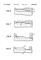
- FIG. 40 is a schematic sectional view of a conventional flash memory
- FIG. 41 is a schematic sectional view of a conventional flash memory.
- FIG. 42 is a schematic sectional view of a conventional flash memory.
- FIG. 43 is a schematic sectional view showing part of a process for manufacturing a flash memory shown in FIG. 24 (a).
- FIG. 44 is a schematic sectional view showing part of a process for manufacturing a flash memory shown in FIG. 24 (a).
- FIG. 45 is a schematic sectional view showing part of a process for manufacturing a flash memory shown in FIG. 24 (a).
- FIG. 46 is a schematic sectional view showing part of a process for manufacturing a flash memory shown in FIG. 24 (a).
- FIG. 47 is a schematic sectional view showing part of a process for manufacturing a flash memory shown in FIG. 24 (a).
- FIG. 48 is a schematic sectional view showing part of a process for manufacturing a flash memory shown in FIG. 24 (a).
- FIG. 49 is a schematic sectional view showing part of a process for manufacturing a flash memory shown in FIG. 24 (a) .
- FIG. 50 is a schematic sectional view showing part of a process for manufacturing a flash memory shown in FIG. 24 (a).
- FIG. 51 is a schematic sectional view showing part of a process for manufacturing a flash memory shown in FIG. 24 (a).
- FIG. 52 is a schematic sectional view showing part of a process for manufacturing a flash memory shown in FIG. 24 (a).
- FIG. 53 is a wiring diagram in which the flash memory of the present invention is arranged in matrix configuration.
- EEPROM electrically erasable and programable memory
- the present invention improves the charge retention characteristic of the floating gate electrode.
- a semiconductor substrate for a flash memory of the present invention one that can be used in normal flash memories can be used.
- Such semiconductor substrates include silicon substrate, GaAs substrate and the like.
- a semiconductor substrate can be used which contains either a p-type or an n-type impurity in advance.
- impurities include boron and the like as p-type impurities and phosphorus and the like as n-type impurities.
- a substrate is preferably used which is deprived of toxic impurities and defects by gettering.
- an inclined portion is provided on the substrate.
- the inclined portion has a height of 100 to 5000 ⁇ and a width of 200 to 8000 ⁇ . The height can be adjusted so that resolution is not deteriorated in exposure. The height is preferably shorter.
- the flash memory of the present invention is also characterized by the fact that the position of one of the two regions is considerably higher than the position of the other region.
- An explanation will be given hereinbelow with respect to a semiconductor in which a source region is located at a position considerably lower than a drain region. However, it goes without saying that the same manufacturing method will be used with respect to a semiconductor device in which a drain region is located at a position considerably lower than the position of the source region.
- the semiconductor device provides a channel region between the source region and the drain region.
- arranging the source region up to the inclined portion allows formation of a device having a short channel.
- Impurities having a conductive type opposite to the substrate are implanted in the source region and the drain region.
- the impurity concentration is 10 19 to 10 21 ions/cm 3 .
- a region having a higher impurity concentration than the bulk and the same conductive type can be provided in the neighborhood of the drain region. Providing such region improves the efficiency of hot electron generation thereby raising the writing speed.
- the channel region can be formed to a sufficient depth which allows the semiconductor device to be free from an influence of profiles that is caused when another impurity region is formed. Preferably such depth assumes Rp 0.1 to 0.4 ⁇ m.
- a floating gate electrode and a control gate electrode are laminated in this order in such a manner that the floating gate electrode and the control gate electrode stretch over the source region and the drain region.
- a gate insulating film is arranged between the substrate and the floating gate electrode, and between the floating gate electrode and the control gate electrode.
- known materials can be used which include polysilicon and the like.
- the impurities concentration or the conductive type thereof can be varied by diffusion or ion implantation.
- the thickness of the floating gate electrode and the control gate electrode is 3000 to 5000 ⁇ .
- the storage capacitance may have a configuration in which the floating gate electrode overlaps the source region.
- a known material can be used as a gate insulating film such as, for example, a film comprising silicon oxide, silicon nitride, tantalum or dielectric substance.
- the gate insulating film may be formed of silicon oxide film-silicon nitride film-silicon oxide film (ONO structure).
- the gate insulating film between the substrate and the floating gate electrode is thinner on the side of the source region than on the side of the drain region (the thinner gate insulating film on the side of the source region is referred to as a first gate insulating film whereas the thicker gate insulating film on the side of the drain region is referred to as the second gate insulating film).
- the thickness of the first gate insulating film and the second gate insulating film ranges between 70 to 100 ⁇ and 100 to 200 ⁇ respectively.
- the thickness of a gate oxide film (the oxide film is hereinafter referred to as a third gate insulating film) between the floating gate electrode and the control gate electrode ranges between 150 to 300 ⁇ both inclusive.
- the third gate insulating film may be thin on the side of the drain region and thick on the side of the source region to improve the lead-in effect.
- an SiN film may be used in one layer of the insulating film. This can prevent an error in erasure by means of internal photoemission or the like.
- a flash memory according to the present invention comprises the above construction.
- the source region may have an LDD structure, DDD structure or profiled lightly doped drain (PLD) structure.
- LDD structure a low concentration region is further formed on the side of a channel region.
- the impurity concentration in the low concentration region ranges between 10 17 to 10.sup. ions/cm 3 both inclusive.
- DDD structure the low concentration region is formed so as to cover the source region.
- the impurity concentration in the low concentration region is 10 18 to 10 19 ions/cm 3 .
- the DDD structure has an advantage that the punch-through is hardly generated compared with the LDD structure.
- an impurity region is formed in such a manner that the region covers the low concentration region of the LDD structure and the source region.
- the impurity concentration in impurity region ranges between 10 17 to 10 19 ions/cm 3 both inclusive.
- These structures serve to improve dielectric strength in erasing operation.
- a damaged region formed in ion implantation in a dose amount of 1 to 9 ⁇ 10 14 ions/cm 2 ) may be diffused so that the region may not overlap another region because of ion implantation for the formation of the low concentration and the high concentration region.
- a smooth side wall spacer may be extended over a side wall of the antioxidant film so that ions are implanted through the side wall spacer. This prevents the overlapping of the region damaged by the profile formed by ion implantation to the silicon immediately below the edge of the antioxidant film.
- This side wall spacer can be easily formed by anisotropic etching or using a two-layer film having a different etching rate.
- the flash memory in the above example takes a two-layer polysilicon structure
- the flash memory can take a three-layer polysilicon structure.
- the flash memory can include an erasing gate.
- a device can be isolated with a gate electrode in place of using a device isolation oxide film.
- a embedded diffusion layer may be provided under the device isolation oxide film.
- a method for manufacturing a flash memory according to the present invention will be detailed hereinbelow.
- a buffer oxide film having a thickness of 1000 ⁇ or more is formed by thermal oxidation.
- This buffer oxide film is formed for obtaining a length of a bird's beak having a good reproducibility, suppressing the generation of the translocation and slippage in the silicon substrate in this region, and alleviating the stress applied to the antioxidant film to be formed in the subsequent process.
- a resist is applied so that a pattern is formed in which only a region for device isolation is open.
- impurities are implanted into the semiconductor substrate.
- the impurities to be implanted may be boron or the like as a P-type impurity, and phosphorous or the like as an n-type impurity.
- the impurity implantation may be conditioned as follows: preferably, the dose amount is 10 12 to 10 13 ions/cm 2 and implantation energy 40 to 200 KeV since impurity ions have to be implanted to a sufficient depth so that the substrate might not be affected by the tail of the ion implantation profile.
- the dose amount and the implantation energy are very important because the hot electron implantation efficiency depends on the concentration.
- the surface concentration is controlled to about 1 to 3 ⁇ 10 16 cm 3 when the last step is completed.
- the subsequent process is to remove the resist, followed by forming an antioxidant film having a thickness of 700 to 1000 ⁇ by the CVD or the like.
- an antioxidant film having a thickness of 700 to 1000 ⁇ by the CVD or the like.
- a silicon nitride film is used as the antioxidant film. This is followed by selectively removing the antioxidant film, by etching using the resist, from the portion where a device isolation region is to be formed.
- the resist is removed, and a spin on glass (SOG) film, a TEOS (Si(OC 2 H 5 ) 4 ) film or the like are coated on the substrate which is followed by forming a side wall spacer on the side wall of the antioxidant film.
- a spin on glass (SOG) film, a TEOS (Si(OC 2 H 5 ) 4 ) film or the like are coated on the substrate which is followed by forming a side wall spacer on the side wall of the antioxidant film.
- impurities are implanted by an implantation energy of 100 to 150 KeV and in a dose amount of 10 13 to 10 14 ions/cm 2 .
- the side wall spacer restricts the implantation of impurities.
- the field dope layer can be formed only in a predetermined region.
- the device isolation oxide film is formed by thermal oxidation (Local Oxidizations method) at 1000° to 1100° C.
- the formation of the device isolation oxide film activates and redistributes the above field dope layer to an inversion prevention layer at the lower layer of the device separation oxide film.
- a layout is designed so that the main portion of the device might not be located therein.
- the antioxidant film is removed by a known method such as dry etching or the like.
- Impurities are implanted to the substrate at implantation energy of 10 to 20 KeV and at the dose amount of 10 15 to 10 16 ions/cm 2 .
- the ion implantation allows impurities to be implanted to a surface buffer oxide film of the substrate except for the region below the device isolation oxide film having a thick thickness.
- impurities that can be used may be such that can be easily taken into a first and a second gate insulating film when such first and second gate insulating films are formed in the later process. Boron is preferable.
- the substrate is annealed so that an active region is formed.
- the annealing is conditioned by a temperature at which impurities can freely activate the buffer oxide film.
- the temperature is such that it exceeds the interface level of a single crystal silicon while it does not exceed the interface level of silicon. This is because the silicon region required a volume of 0.43 to 0.44 (Si/SiO 2 ) for forming a unit volume of the first gate insulating film. Temperatures of 800° to 900° C. is used for the purpose.
- the active region and a region where a source region is to be formed are opened by using a resist or the like.
- the resist is used as a mask to remove the buffer oxide film and the device isolation region in the opening.
- a known method can be used for removing the device isolation region, but the use of an etchant that affects a silicon interface is not preferable. Nor dry etching is preferable. As a preferable etching method, for example wet etching using HF can be used.
- the inclined portion formed by oxidation assumes a smooth configuration as compared with the inclination formed by etching.
- the stepped portion can be more favorably coated, which allows reducing stress on a floating gate electrode or the like which will be formed in the subsequent step, thereby improving the reliability of a device that will be miniaturized.
- the oxidation has an advantage that it causes smaller damage to the silicon interface than etching thereby allowing manufacturing a stable device.
- the length of the bird's beak that affects the size of the inclined portion can be easily controlled by controlling the thickness of the buffer oxide film. Then, the minute measurement of the buffer oxide film can be easily adjusted.
- the insulating film can be formed by thermal oxidation.
- the method for oxidation can be determined in consideration of the kind of device and the alignment between processes.
- the method for oxidation include, for example, oxidation using dry O 2 , pyrogeneratic oxidation and the like.
- the oxidation temperature may be relatively low ranging between 850° and 950° C.
- the oxidation is performed at about 900° C. (in the oxidation at 900° C., since boron impurities are diffused, the resulting device has an inner channel structure).
- the oxide film formed by using the dry O 2 (the pyrogeneratic oxidation may be used to reduce the trap level) has many advantages such as the largest activated energy which allows easy control of the oxide film, excellent dielectric strength properties, no shift in the threshold value and no increase in the trap density in the oxide film.
- Such oxidation oxidizes exposed substrate with the result that the thickness of the oxide film of the inclined portion at a portion where the device isolation oxide film is removed becomes thinner than the thickness of the oxide film at the portion of the buffer oxide film.
- the insulating film at the inclined portion serves as the first gate insulating film whereas the insulating film at the buffer oxide film portion serves as the second gate insulating film.
- the impurities implanted in at the aforementioned step diffuse inside of the insulating film so that the first and the second gate insulating film contribute toward improving the properties as a tunnel insulating film with respect to the electric field, thereby exhibiting an advantage of enhancing endurance with respect to the repetitive rewriting operation.
- an inactive substance which can further thermal oxidation such as argon or the like, can be preliminarily implanted to a region where the second gate insulating film is formed either with or in combination with the aforementioned impurity implantation.
- Si ions may be implanted to a region where the second gate insulating film is formed so that the bonding force of Si crystal can be weakened.
- Such Si ion implantation is advantageous in suppressing diffusion of impurities into the substrate in the buffer oxide film.
- the substrate after the formation of the insulating film, the substrate can be subjected to annealing in the atmosphere of H 2 for adjusting the impurity concentration in the insulating film.
- the substrate Since the substrate is oxidized at relatively low temperature, a high interface fixing electric load is generated in the insulating film.
- the high electric load can be reduced by subjecting the substrate to annealing in the inactive atmosphere of N 2 , Ar or the like.
- the region where the first and the second gate insulating films are formed are subjected to sacrificial oxidation before the formation of the first and the second gate insulating films, more favorable insulating films can be formed.
- the tunnel insulating film may use a laminate layer of a HTO film and a thermal oxide film.
- polysilicon or the like is laminated on the entire surface of the substrate by CVD or the like followed by etching to form a floating gate electrode at a desired position of the substrate.
- a source and a drain region are formed with the floating gate electrode serving as a mask by impurity implantation.
- conditions for impurity implantation can be an implantation energy of 30 to 80 KeV, a dose amount of 10 15 to 10 16 ions/cm 2 .
- the impurity is also implanted into the floating gate electrode.
- the dose amount of the impurity depends on the area and the thickness of the insulating film so that the coupling capacity between the floating gate electrode and the periphery thereof assumes an appropriate value.
- a deeper channel region can be formed by implanting Si ions to the inclined portion of the channel region.
- a third gate insulating film is formed by subjecting the floating gate electrode to oxidation or by other methods.
- a control gate electrode is formed by laminating polysilicon or the like on the entire surface of the third gate insulating film, followed by etching the polysilicon or the like to form a control electrode. Furthermore, the entire surface on the substrate is subjected to oxidation to form an oxide film thereon. The subsequent step is to etch the floating gate electrode and the control gate electrode in self-alignment using the resist.
- an interlayer insulating film is laminated, a contact hole is opened, and a passivation film is formed by metallization which allows forming a flash memory having a self-alignment structure.
- An LDD structure can be formed by impurity implantation after the floating gate electrode and the control gate electrode are etched in self-alignment.
- the implantation conditions can be an implantation energy of 40 to 80 KeV and a dose amount of 10 14 to 10 16 ions/cm 2 .
- a DDD structure can be formed by ion implantation of a high concentration of 75 As + after ion implantation of a low concentration of 31 P + .
- the implantation condition of 75 As + is an implantation energy of 30 to 80 KeV and a dose amount of 10 14 to 10 16 ions/cm 2 .
- a PLD structure can be formed by gradually changing an implantation angle and an implantation energy.
- the implantation conditions can be an implantation energy of 20 to 100 KeV, an implantation angle of 30° to 70° and a dose amount of 10 13 to 10 16 ions/cm 2 .
- the implantation conditions may preferably be divided so that a peak concentration of the ion implantation profile assumes about 10 19 to 10 21 ions/cm 2 .
- what is important here is to set a sufficient cool-off period between implantations.
- As ions may be implanted at an implantation energy of 80 KeV and a dose amount of 2 ⁇ 10 15 ions/cm 2 , an implantation energy of 40 KeV and an dose amount of 1.5 ⁇ 10 15 ions/cm 2 and an implantation energy of 20 KeV and a dose amount of 7 ⁇ 10 14 ions/cm 2 .
- the method for forming a flash memory according to the present invention a process has been proposed in which the gate insulating film depends on the dose amount of the substrate.
- the method in accordance with the present invention is not so limited. It goes without saying that the flash memory of the present invention can be manufactured in the method identical to the conventional method. When the conventional method is used for manufacturing the flash memory of the present invention, further cleaning and automation processes as well as extremely severe process control will be necessary. Additionally, since the present invention does not use an offset gate, a bulk may be used in which a channel dope layer is formed to form with good accuracy an erasing gate insulating film.
- FIGS. 37 and 39 an electric connection of the flash memory according to the present invention will be explained hereinbelow.
- Vse designates a erasing voltage applied to the source region 10, Vfg an electric potential at the floating gate electrode 7, C4 a parasitic capacitance between the control gate electrode 9 and the floating gate electrode 7, C3 a capacitance between the floating gate electrode 7 and the substrate 37, C2 a capacitance between the floating gate 7 and the substrate 38 and C1 a capacitance between the floating gate electrode 7 and the drain region 11.
- the electric field Ee (erasing) applied to the inside of the second gate insulating film 6 can be briefly represented by the following equation (1):
- Erasing memory by using a tunnel effect requires controlling the appropriate thickness d2. This result in an extreme increase in C1 and reduction in Ee in the absence of the control of an area between the second insulating film 6 and the source region 10. Consequently, the present invention provides a simple method for manufacturing a flash memory, which method allows selecting optimal capacitances described above and securing a definite level of yield ratio to obtain a desired Ee.
- the present invention allows appropriately setting properties of each region for producing C1 to C4, such as an area, a thickness and quality of films and eliminating the non-uniformity in the manufacture of flash memories. Consequently, when memories become finer, writing and erasing properties can be maintained.
- a flash memory and a method for manufacturing the same will be explained in conjunction with the drawings when the flash memory is applied to a self-aligned flash memory cell transistor.
- FIG. 1 shows a view showing a structure of a cross section of a single cell in a flash memory according to a first example of the present invention.
- reference numeral 1 designates a P-type semiconductor substrate, 2 a field dope layer, 3 a device isolation oxide film (LOCOS), 4 a channel region, 5 a first gate insulating film, 6 a second insulating film provided on the inclined portion and formed from the channel region 4, 7 a first polysilicon layer (floating gate electrode), 8 a third gate insulating film, 9 a second polysilicon layer (control gate electrode), 10 a source region (N + type impurity region), 11 a drain region (N + type impurity region) and 12 an LDD region for improving the dielectric strength in the operation of erasing data in the memory.
- LOC device isolation oxide film
- Example 1 of the flash memory is that the second gate insulating film 6 which discharges an electric load at the time of erasing data in the memory is formed in the inclined portion of the length of the bird's beak (about 0.6-0.8 ⁇ m).
- the second gate insulating film 6 is characterized by being formed on the channel dope layer region 4 predetermined and controlled with high accuracy in the silicon substrate 1.
- data is written in the flash memory by the application of a high voltage to the drain region 11 and the control gate 9 followed by the absorption of the resulting hot carriers into the control gate 9 and the subsequent accumulation of the hot carriers in the floating gate electrode 7.
- data is erased by the application of a high voltage to the source region with the control gate electrode 9 grounded, followed by the discharge of the accumulated electric load in the floating gate electrode 7 using the F-N tunnel injection.
- the electric load is discharged at this time through the thin second gate insulating film 6 formed inside of the inclined portion.
- the source region 10 is formed in a region where are originally device isolated region.
- the carrier electric load takes a form of heading from the lower part of the drain region 11 to the Upper part thereof. In this manner, the carrier electric loads progresses with a definite angle relative to the first gate insulating film 5.
- the first gate insulating film is formed on the inclined portion of the silicon substrate formed by LOCOS oxidation, a pure insulating film can be formed which contains an extremely small amount of impurities.
- the second gate insulating film is formed on the silicon substrate with a surface direction 100, containing a high concentration of impurities such as boron or the like. As a consequence, a large amount of impurities are contained in the second gate insulating film. These impurities serve as hot carriers in the second gate insulating film, largely improving the properties of acquiring the electrons in the neighborhood of the pinch-off point to improve the efficiency at which data is written into the memory.
- a flash memory can be obtained which is excellent in writing and erasing properties, electric load holding properties and rewriting endurance.
- a thicker second gate insulating film and a thinner first gate insulating film improve the basic operation of the flash memory that is repeated in which data is written into the floating gate electrode with the electric field of the control gate electrode and data is erased with the electric field of the source electrode. Still furthermore, adjustment of the capacitance coupling of the insulating film with each electrode or source and drain regions allows improvement of the basic operation.
- the channel below the first gate insulating film is more strongly inverted than a channel below the second gate insulating film.
- electrons under the floating gate electrode can move more easily to facilitate the writing operation.
- FIGS. 2 through 13 are sectional views showing a single cell for use in illustrating a method for manufacturing a self-aligned non-volatile flash memory according to the present invention.
- the amount of the first gate electrode and the source region was appropriately adjusted in accordance with the design rule.
- a buffer oxide film 22 was grown to a thickness of 1000 ⁇ .
- the buffer oxide film was preferably formed to a thickness of 1000 ⁇ or more. In this particular example, 0.8 micron long bird's beak length was formed.
- a resist pattern 23 was formed which was open only in the device formation region.
- boron was implanted in a dose amount of 5 ⁇ 10 12 ions/cm 2 and at an implantation energy of 100 KeV to a sufficient depth (Rp 0.3 micron or more) which would not be affected by the tail of the profile formed by the implantation of a high concentration of boron.
- a channel dope layer 24 was formed. Ions has to be implanted with an extremely clean device and in an extremely clean environment. Thus an ion implantation equipment was used which does not sputter heavy ions.
- the resist pattern was removed to deposit to a thickness of 1000 ⁇ a silicon nitride film 25 which constitutes an antioxidant film. Then on the silicon nitride a resist pattern 26 was formed which was only open in a region where a device isolation oxide film was formed for isolating the device region into an island configuration. Selectively removing the silicon nitride film using the resist pattern 26 as a mask allowed the formation of a silicon nitride film pattern 25 which was open at a portion where the device isolation oxide film was formed.
- a side wall spacer 27 for restricting the passage of ion implantation was formed on the side wall of the open part of the silicon nitride film pattern 25.
- boron ions were implanted for the formation of a channel stopper at an implantation energy of 40 KeV and in a dose amount of 5 ⁇ 10 13 ions/cm 2 to form a field dope layer 28.
- the substrate was subjected to wet oxidation (so-called local oxidation method) at 1000° C. to grow a silicon oxide film on the exposed surface of the substrate 1, thereby forming a device isolation oxide film 29.
- the substrate on which the device isolation oxide film was formed to a thickness of about 1 ⁇ m is etched by about 4300 to 4400 ⁇ .
- boron atoms in the field dope layer 28 were activated and redistributed to form an inversion prevention layer 30 on the lower layer of the field channel oxide film 29.
- the silicon nitride film pattern 25 was removed by dry etching. Boron was implanted at an implantation energy of 15 KeV and in a dose amount of 5 ⁇ 10 15 ions/cm 2 into the buffer oxide film 22.
- the substrate was subjected to annealing at 850° C. to form a P + type impurity layer 31 on the surface of the device activation region. Boron was implanted in an environment of high degree of cleanliness.
- the substrate was annealed at the temperature at which boron was freely activated in the buffer oxide film 22 and at the temperature of the activation energy which exceeded the interface level of a single crystal silicon and did not exceed the counterpart of polysilicon.
- the P + -type impurity layer 31 was extremely similar to the deposited layer.
- the P + type impurity layer 31 boron was implanted in a high concentration (with a surface concentration of 3 ⁇ 10 15 ions/cm 2 or more) into a region in the neighborhood of a transition layer (SiO, SiO 2 O, Si 2 O 3 , SiOx layer) between the silicon substrate and the oxide film and an extremely shallow region having a thickness of about 100 ⁇ or the less on the surface layer on the side of the substrate.
- the P + type impurity layer 31 was an extremely thin layer whose surface resistance could not be measured by the four probe method. Thus, the conditions required for the formation of the P + type impurity layer 31 could not be theoretically determined, but they could be determined only from experience.
- this measurement method comprised forming on a wafer a TEG pattern for the hole measurement, selectively etching an layer to be evaluated with anode oxidation by using an electrolyte such as tetrahydrofurfuryl alcohol and measuring the thickness of the anode oxide film until reaching the silicon substrate to calculate the depth of the P + type impurity layer 31 from the measurement.
- the gate insulating film was formed at 900° C., which was the highest temperature in consideration of the inner diffusion constant of the P + type impurity layer 31 in the direction of the substrate. With respect to the generated oxide film properties resulting from the low temperature oxidation, adjusting alignment was required at the subsequent step.
- the process might be modified to one in which the silicon bonding force was weakened in an extremely shallow portion of the silicon to be oxidized by implanting a high concentration of silicon to a region where the P + type impurity layer was formed in place of implanting boron to the buffer oxide film 22.
- a resist pattern 32 was formed which was open at a device region where an active region and a source region were to be formed at the subsequent step.
- the buffer oxide film 22 and part of the device isolation oxide film was removed by wet etching using a clean HF solution, thereby forming an active region.
- the buffer oxide film region was overetched and the etching process required about 10 minutes. Part of the surface of the P + type impurity layer 31 was etched.
- the resist pattern 32 was peeled off, thermally oxidized, followed by forming a first and a second gate insulating film (33,34) on the exposed surface of the substrate in the same oxidation process.
- a first and a second gate insulating film 33,34
- the depth of the P + type impurity layer 31 could be adjusted, and a stable gate insulating film could be provided.
- the sacrificial oxidation was effective when combined with H 2 annealing after oixdation.
- the kind of oxidation to be used was determined in view of the kind of device and self-alignment of the process.
- This example adopted dry O 2 oxidation.
- the P + type impurity layer 31 was formed on the exposed surface other than a region where the device isolation oxide film was formed.
- the boron concentration on the surface of the layer was controlled to a concentration exceeding 3 ⁇ 10 20 ions/cm 2 .
- the surface boron concentration in the bird's beak length region was controlled to a level almost equal to that of the substrate concentration.
- the substrate was oxidized in dry O 2 using a vertical type furnace at 900° C. for 15 minutes thereby forming a second gate insulating film 33 having a thickness of about 10 nm in the channel region 24.
- a first gate insulating film 34 having a thickness of about 15 to 20 nm.
- the oxidation resulted in the depletion of silicon in the P + type impurity layer 31 formed on the surface of the substrate.
- boron had smaller segregation coefficient on the silicon interface compared with phosphorus and arsenic so that boron was incorporated in the thermal oxidation film.
- boron had a larger diffusion coefficient in the silicon oxidation film than in silicon, this degree of temperature promotes a little redistribution in silicon, thereby promoting diffusion of boron to the outside. Consequently, the first gate insulating film contained a large amount of boron.
- Impurities in these gate insulating film contribute to the improvement of properties of the tunnel oxide film with respect to the electric field unless the amount of impurities exceeds a certain level.
- the impurities exhibit an effect of enhancing the endurance against repeated rewriting of data in the memory.
- Adjustment of the boron concentration in the oxide film by annealing in H 2 after the formation of the gate insulating film provide still more stable rewriting properties.
- oxidation at low temperatures generates a high interface (fixing) electric load in the gate insulating oxide film.
- the high interface electric load can be reduced by annealing in inactive atmosphere (for example, N 2 , Ar or the like) after the formation of the gate insulating film (see FIG. 9).
- polysilicon film was grown to 1500 ⁇ on the entire surface by CVD.
- the polysilicon film was etched by using the resist pattern. After the floating gate electrode 35 was formed, the resist pattern was removed.
- a source region 36 and a drain region 37 were formed by ion implanting As ions at an implantation energy of 40 KeV and at dose amount of 5 ⁇ 10 15 ions using the device isolation oxide film and the floating gate as a mask.
- the floating gate electrode was doped with n-type impurities. An additional amount of the impurities might be implanted into the source region at higher energy. Otherwise, an additional amount of impurities might be implanted to the drain region which had a higher concentration than the channel region with the same conductive type as the channel region. Still otherwise, As and P ions might be simultaneously implanted.
- the surface of the floating gate electrode 35 was oxidized and the third gate insulating film 38 was formed to a thickness of about 20 to 30 nm.
- the third gate insulating film 38 with a favorable uniformity could be provided.
- polysilicon film was formed to a thickness of about 2500 ⁇ on the entire surface of the substrate by CVD or the like for the formation of a control gate electrode.
- the control gate electrode might comprise two layers of polysilicon and WSi.
- an oxide silicon film 40 was formed to a thickness of about 1500 ⁇ by CVD.
- the oxide silicon film and the polysilicon film were subsequently patterned by etching using a mask 41 comprising a resist film thereby forming a control gate 39.
- the floating gate electrode 35a extending from the lower part of the control gate electrode to the source region was etched to realize a self-aligned arrangement.
- the low concentration diffusion layer 42 overlapped the floating gate electrode at an appropriate portion by subsequent heat treatment.
- As ions might be implanted by rotating the substrate through an angle of about 60° so that the required overlap might be facilitated.
- the surface concentration of the source region which overlaps the gate electrode preferably assumes 10 18 /cm 3 or less in the low concentration layer and 10 19 /cm 3 or more in the high concentration layer when the gate oxide film has a thickness of 60 to 100 ⁇ .
- an interlayer insulating film 43 was formed in accordance with the normal process.
- a contact hole was opened on the substrate and the substrate was subjected to metallization 44 so that a passivation film (not shown in the drawings) was formed.
- a flash memory having a self-aligned structure was completed which used the present invention (see FIG. 1).
- the writing operation will be explained initially.
- a voltage of 5 V was applied to the drain region and a voltage of 12 V was applied to the control gate electrode after the source region was grounded, electrons flowed from the source region to the drain region at a high electric field, and electrons were then generated which could exceed an energy barrier from the silicon surface to the insulating film in the neighborhood of the drain region.
- the source region was formed at a region relatively lower than the drain region with the result that the electrons in the high electric field were directed to the insulating film in the neighborhood of the drain region at a predetermined angle. Consequently, the electrons were more easily absorbed into the electric field of the control gate electrode, which improved the writing performance of the flash memory.
- the erasing operation was performed in the same manner as the conventional method.
- Application of an erasing voltage resulted in the discharge of the electric field from the floating gate electrode to the side of the source region.
- the insulating film in the neighborhood of the source region could be thinned down to about 10 nm, so that the erasing speed could be heightened.
- Data could be read from the flash memory by checking the presence of current which flowed from the drain region when a voltage of 5 V was applied to the drain region and the control gate electrode.
- the gate insulating film was covered almost completely with a thick gate insulating film.
- the insulating film for erasure which was located in the neighborhood of the source region that had been thinned was formed with an inclination thereby making it difficult for F-N tunneling to be generated.
- the flash memory in the above embodiment assumes an LDD structure, but it can assume a DDD structure.
- symbol 110 designates a low concentration impurity area in the source region, and 112 a high concentration impurity area in the source region.
- FIG. 15 is a view showing an example in which a concept of the present invention is applied to a flash memory of an offset gate type.
- the insulating film for erasure was provided on an inclined region more steep than the flash memory of self-alignment type. Therefore, the bird's beak length was set to 0.7 micron (the buffer oxide film is set to 500 ⁇ .)
- FIG. 16 is a view showing the flash memory according to one example of the present invention. An area on the upper part of the floating gate electrode was enlarged to a size larger than an area under the lower part of the floating gate.
- the flash memory was manufactured in the same manner as Example 1 except that the flash memory was manufactured according to the following method.
- a floating gate electrode was formed and then an oxide film was formed thereon. Subsequently, a resist pattern was formed which had an opening on the floating gate electrode of the drain region side. The resist pattern was used as a mask to remove the oxide film at the opening by RIE. After polysilicon was laminated on the entire surface of the substrate, the substrate was etched back by anisotropic etching, thereby removing polysilicon deposited on a portion other than the side wall of the opening of the insulating film. Furthermore, the removal of the oxide film resulted in the formation of a floating gate electrode having a projecting part.
- FIG. 17 is a view showing one example in which the device isolation by the device isolation oxide film on one side was replaced by the device isolation by the gate electrode 51.
- a third gate insulating film is formed in such a manner that the insulating film was thin on the side of the drain region and thick on the side of the source region.
- the flash memory allowed improving the drawing efficiency with the control gate electrode.
- FIG. 18 is a view showing one example of the flash memory in which the same advantage was provided by selectively implanting phosphorus impurities and forming an insulating film having a different dielectric rate instead of changing the thickness of the first and the second gate insulating film.
- the dielectric rate of the first gate insulating film 65 was 3.5 whereas the counterpart of the second gate insulating film 66 was 3.9.
- a capacitance coupling between the floating gate electrode and the control gate electrode contributed largely to the selective writing properties.
- the capacity coupling between the floating gate electrode to which a writing signal is applied and drain region constitutes a very important factor.
- FIGS. 19 through 21 shows a device in which the floating gate electrode is extended on the drain region with an insulating film sandwiched therebetween, the drain region is used as a control gate electrode to increase the coupling capacity to improve the writing efficiency.
- uneven patterns are provided on the drain region, the coupling depth of the trench region is changed, and a trench is provided in the drain region to increase the capacity coupling.
- the same bias is applied to the drain region and the control gate electrode which makes it very difficult to stabilize the pinch-off.
- a ferroelectric film is preferably provided on the gate insulating film of the source side, and a high concentration of impurities more preferably dope in the channel region of the drain side.
- the device was isolated with the gate 53.
- the floating gate electrode and the device isolation gate were formed at the same step.
- the gate was used as a mask to form the source and drain regions.
- Such structure allowed conduction between source regions adjacent to the device isolation gate 53 to be realized in a flexible manner.
- the device isolation gate might be realized with the floating gate electrode and the control gate electrode. This enabled setting the degree of device isolation by selecting in advance the floating gate electrode to accumulate electric loads.
- a diffusion layer 52 was formed which had a little higher concentration than the channel region in such a manner that the diffusion layer covered the drain region 11 formed under the floating gate electrode 7. Symbol A designates a pinch-off point in FIG. 22.
- a device shown in FIG. 1 might be formed in a well 45.
- the conductive type of this well might be of the same as or the reverse of the substrate.
- FIGS. 24 (a) to (c) a device might be formed in which the source region was formed above the drain region.
- the substrate surface direction might be used for the channel region on the source side.
- FIG. 24 (a) is a schematic view of a cell
- FIG. 24 (b) is an expanded view of portion A of the floating gate electrode
- FIG. 24 (c) is a view further expanding the inclined portion of the channel region.
- reference numeral 201 designates a P-type semiconductor substrate, 204 a channel region, 205 a first gate oxide film, 206 a second gate insulating film provided on an inclined portion and formed in the semiconductor substrate, 207 a floating gate electrode, 208 a third gate insulating film, 209 a control gate electrode, 210 a source region, 211 a drain region, 212 a LDD region for improving dielectric strength at the erasing operation.
- the device shown in FIG. 24 (a) was manufactured in the following manner.
- the device isolation oxide film 29 below the silicon nitride film 25 was etched in a predetermined amount.
- the SOG (spin on glass) film 215 was coated through an appropriate etch-backing (see FIG. 45).
- gate insulating film 216 The entire surface thereof was thermal oxidized to form gate insulating film 216 (see FIG. 48).
- a polysilicon layer was formed on the entire surface thereof and the polysilicon layer was etched by using a resist pattern to form a floating gate electrode 217 (see FIG. 49).
- the device isolation oxide film 29 and the floating gate electrode 217 were used as a mask to implant a high concentration impurity to form the source region 210 and the drain region 211 (see FIG. 50).
- the source region was formed in a shallow configuration than the drain region 211 so that the source region 210 was formed by implanting impurities through the gate insulating film 216.
- the surface of the floating gate electrode 217 was oxidized to form the third gate insulating film 208.
- the polysilicon layer is formed on the entire surface.
- the resist pattern was used to etch the polysilicon layer thereby forming a control gate electrode 209 through the oxidation process (see FIG. 51).
- control gate electrode 209 and the end of the floating gate electrode 217 are aligned to each other to oxidize the entire surface thereof. Then, impurities are implanted in the diagonal direction while rotating the substrate to form an LDD region 212 below the floating gate electrode 217 on the side of the source region (see FIG. 52).
- the direction in which electrons that have been traveling through the channel being accelerated from the source region to the drain region are bent in the configuration of the channel region when the electrons enter into the inclined portion. Consequently, a high electric field is generated as a result of the bent progression direction of the electrons in the substrate (bent in the dislocation composite defect portion resulting from an edge stress at the LOCOS oxidation though it is difficult to describe in an accurate way) and the overlapping of the end portion of the depletion layer of the drain region onto the inclined portion.
- the high electric field and the bent of the progression direction of electrons promotes the generation of hot electrons.
- the inclined surface (approximate to a (111) surface) of the silicon substrate is used as a material to form a gate oxide film on the side of the drain region. Consequently, the top of the inclined surface on the drain region is formed thicker than the side of the source region in the same thermal oxidation process. This facilitates a countermeasure against an error in erasure at the time of reading data as compared with device in which the drain region is located above the source region. In other words, the process for forming the impurity layer 31 can be omitted which is regarded at the most difficult on the practical level.
- d1 designates a thickness of a gate insulating film in the planar channel region
- d2 a thickness of a gate insulating film in the inclined channel region
- ⁇ ox a conductive rate thereof
- ⁇ n a mobility of electrons
- W a channel width. It is assumed that the conductive rate of the gate insulating film in the planar channel region and that of the gate insulating film in the inclined channel region are the same.
- Vt designates a threshold value with respect to the floating gate electrode, which depends on the effective channel length I.
- Vf designates a potential of the floating gate electrode, which is represented by the following formula; ##EQU2##
- symbol Cfs designates a capacity between the floating gate electrode and the source region.
- Symbol Cfss1 designates a capacity between the floating gate electrode and the inclined channel region.
- Symbol Cfss2 designates a capacity between the floating gate electrode and the planar channel region.
- Symbol Cfd designates a capacity between the floating gate electrode and the drain region, and Cfc a capacity between the floating gate electrode and the control gate electrode.
- Symbol Qf designates an electric load generated in the floating gate electrode when current flowing through the channel region is accelerated in the electric field between the source and the drain regions and electrons which acquired a sufficient energy is injected into the floating gate electrode.
- the electric load designated by symbol Qf depends on the rate ⁇ at which hot carrier is injected into the gate insulating film.
- the time integral of ⁇ Id at the channel current of Id is given by the following formula: ##EQU3##
- Symbol S1 designates a sum of the overlapped area of effective channel length ( Ii+I2!W), the floating gate electrode and the source region.
- the writing time of the memory transistor Tw can be represented by the function of the following formula by integrating the sum. ##EQU7##
- Cfss1 and Cfss2 are determined by the thicknesses d1 and d2 and by the adjustment of I1 and I2 to an optimal value by process conditioning, the writing time adjustment can be facilitated than the conventional structure with the adjustment of this value. As described above, a bent is generated in the channel current with the result that the implantation efficiency can be improved at that portion.
- the rotation ion implantation method was used to secure a overlap amount with the floating gate electrode in the formation of a low concentration region in the source region.
- the approximately entire region of the inclined region could be a low concentration source region.
- a resist pattern 43 was formed which had an opening at least on part of the active region and on the device isolation region where the source region was formed with the silicon nitride pattern 25 left as it was.
- the resist pattern 43 and the silicon nitride film 25 are used as a mask to remove part of the device isolation oxide film 29 by wet etching with a clean HF solution of (see FIG. 27). Later, the resist pattern 43 was peeled off and the silicon nitride film pattern 25 was removed which was followed by implanting As ions at 10 KeV in a low concentration for the formation of the low concentration source region.
- the buffer oxide film 22 was etched with the clean HF solution, followed by thermal oxidation to form a gate insulating film 46 on the exposed surface of the substrate 1. Then, by CVD, a polysilicon film, an oxide film, a polysilicon film, an oxide film and a resist pattern 47 was formed in this order (see FIG. 31). After the resist pattern 47 was used as a mask to form a control gate electrode and a floating gate electrode, the resist pattern 47 was removed. After oxidation step, the device isolation film, the control gate electrode and the floating gate electrode were used as a mask to implant a high concentration of As ions thereby forming the source region 36 and the drain region 37 (see FIG. 32).
- a height difference between the upper surfaces of the source region 36 and the drain region 37 is preferably 5 ⁇ m or less.
- the bird's beak length is preferably 0.6 to 0.8 ⁇ m.
- data could be written into the memory by grounding the source region and then applying a voltage to the drain region and the control gate electrode.
- the applied voltage is shown in the following table.
- FIG. 33 is a model view showing the above writing operation.
- reference numeral 47 designates a row address line whereas 48 a column address line, and 49 a erasing line.
- FIG. 34 is a model view showing the above operation.
- FIG. 35 symbol--designates a hot electron in which arrows indicate that hot electrons at the pinch-off point progressed toward the floating gate electrode with a definite angle.
- FIG. 36 shows a memory cell array of NOR type.
- reference numeral 84 designates a memory site where the flash memory of the present invention was arranged, 85 a row address line, and a signal line wired from a row address decoder 86.
- Reference numeral 87 designates a column address line, and a signal line wired from a column address decoder 88.
- Reference numeral 89 designates an erasing line, and a signal line wired from a source decoder 90.
- either of the source region or the drain region is positioned below the rest thereof which enables substantially extending the length of the channel region. Therefore the present invention has an advantage that a punch-through hardly occurs as compared with the same two-dimension design rule.
- the present invention allows realization of a flash memory which has a small area, a rapid writing and erasing speed, and erroneous erasure of data can be prevented in reading operation. Since such flash memory is excellent in large amount production and miniaturization, and has an extremely excellent endurance against frequent writing, erasing and reading operation, the flash memory has an insurmountable industrial value as an image processing memory used for frequently executing simple operations of a large amount of data or as a device which can substitute a magnetic memory.
- each of these cells receives 13 V when data is erased from the memory thereby eliminating the electric load.
- cells can be formed having a thick gate insulating film on the drain side and a thin source side to be bilaterally arranged and connected centering on the drain region thereby forming a memory cell matrix.
Abstract
Description
Ee=Vse (c5+C4+c3+c2)/d2 (C1+C2+C3+C4+C5) Equation (1)
Vfg=Vgw (C4/(C4+C2+C3+C5+C1)) Equation (2)
______________________________________
source region       0 V       0 V
control gate electrode
                    10 V      12 V
drain region        4 V       6 V
______________________________________
______________________________________
source region       10 V       13 V
control gate electrode
                    0 V        0 V
drain region        open       open
______________________________________
Claims (17)
Priority Applications (1)
| Application Number | Priority Date | Filing Date | Title |
|---|---|---|---|
| US08/452,695 US5591652A (en) | 1993-11-08 | 1995-05-30 | Method of manufacturing flash memory with inclined channel region |
Applications Claiming Priority (2)
| Application Number | Priority Date | Filing Date | Title |
|---|---|---|---|
| JP5-278209 | 1993-11-08 | ||
| JP27820993A JP3159850B2 (en) | 1993-11-08 | 1993-11-08 | Nonvolatile semiconductor memory device and method of manufacturing the same |
Related Child Applications (1)
| Application Number | Title | Priority Date | Filing Date |
|---|---|---|---|
| US08/452,695 Division US5591652A (en) | 1993-11-08 | 1995-05-30 | Method of manufacturing flash memory with inclined channel region |
Publications (1)
| Publication Number | Publication Date |
|---|---|
| US5502321A true US5502321A (en) | 1996-03-26 |
Family
ID=17594122
Family Applications (2)
| Application Number | Title | Priority Date | Filing Date |
|---|---|---|---|
| US08/327,910 Expired - Lifetime US5502321A (en) | 1993-11-08 | 1994-10-24 | Flash memory having inclined channel |
| US08/452,695 Expired - Lifetime US5591652A (en) | 1993-11-08 | 1995-05-30 | Method of manufacturing flash memory with inclined channel region |
Family Applications After (1)
| Application Number | Title | Priority Date | Filing Date |
|---|---|---|---|
| US08/452,695 Expired - Lifetime US5591652A (en) | 1993-11-08 | 1995-05-30 | Method of manufacturing flash memory with inclined channel region |
Country Status (3)
| Country | Link |
|---|---|
| US (2) | US5502321A (en) |
| JP (1) | JP3159850B2 (en) |
| KR (1) | KR100221062B1 (en) |
Cited By (46)
| Publication number | Priority date | Publication date | Assignee | Title |
|---|---|---|---|---|
| US5556799A (en) * | 1995-11-13 | 1996-09-17 | United Microelectronics Corporation | Process for fabricating a flash EEPROM |
| US5569946A (en) * | 1994-09-12 | 1996-10-29 | United Microelectronics Corporation | Flash memory cell with self-aligned tunnel dielectric area above LDD structure |
| US5576569A (en) * | 1994-05-06 | 1996-11-19 | United Microelectronics Corporation | Electrically programmable and erasable memory device with depression in lightly-doped source |
| WO1997047047A1 (en) * | 1996-06-04 | 1997-12-11 | Advanced Micro Devices, Inc. | Short channel flash eeprom device having a double diffused source and method of manufacturing the same |
| US5721448A (en) * | 1996-07-30 | 1998-02-24 | International Business Machines Corporation | Integrated circuit chip having isolation trenches composed of a dielectric layer with oxidation catalyst material |
| US5741737A (en) * | 1996-06-27 | 1998-04-21 | Cypress Semiconductor Corporation | MOS transistor with ramped gate oxide thickness and method for making same |
| US5757059A (en) * | 1996-07-30 | 1998-05-26 | International Business Machines Corporation | Insulated gate field effect transistor |
| EP0847091A2 (en) * | 1996-12-06 | 1998-06-10 | Halo Lsi Design and Device Technology Inc. | Low voltage eeprom/nvram transistors and making method |
| US5777359A (en) * | 1995-12-27 | 1998-07-07 | Lg Semicon Co., Ltd. | Semiconductor flash memory device and fabrication method of same |
| US5780889A (en) * | 1995-11-22 | 1998-07-14 | Cypress Semiconductor Corp. | Gate overlap drain source flash structure |
| US5780893A (en) * | 1995-12-28 | 1998-07-14 | Nippon Steel Corporation | Non-volatile semiconductor memory device including memory transistor with a composite gate structure |
| US5844271A (en) * | 1995-08-21 | 1998-12-01 | Cypress Semiconductor Corp. | Single layer polycrystalline silicon split-gate EEPROM cell having a buried control gate |
| US5897354A (en) * | 1996-12-17 | 1999-04-27 | Cypress Semiconductor Corporation | Method of forming a non-volatile memory device with ramped tunnel dielectric layer |
| EP0935293A2 (en) * | 1998-01-16 | 1999-08-11 | Matsushita Electric Industrial Co., Ltd. | Nonvolatile semiconductor memory device and method for fabricating the same, and semiconductor integrated circuit device |
| US5982669A (en) * | 1998-11-04 | 1999-11-09 | National Semiconductor Corporation | EPROM and flash memory cells with source-side injection |
| US6103575A (en) * | 1998-03-30 | 2000-08-15 | Worldwide Semiconductor Manufacturing Corporation | Method of forming a single poly cylindrical flash memory cell having high coupling ratio |
| US6147379A (en) * | 1998-04-13 | 2000-11-14 | Matsushita Electric Industrial Co., Ltd. | Semiconductor device and method for fabricating the same |
| US6190926B1 (en) * | 1996-10-08 | 2001-02-20 | Ramtron International Corporation | Yield enhancement technique for integrated circuit processing to reduce effects of undesired dielectric moisture retention and subsequent hydrogen out-diffusion |
| US6190968B1 (en) | 1998-11-04 | 2001-02-20 | National Semiconductor Corporation | Method for forming EPROM and flash memory cells with source-side injection |
| US6211547B1 (en) * | 1997-11-24 | 2001-04-03 | Winbond Electronics Corporation | Semiconductor memory array with buried drain lines and processing methods therefor |
| US6232633B1 (en) * | 1998-06-08 | 2001-05-15 | International Business Machines Corporation | NVRAM cell using sharp tip for tunnel erase |
| US6262452B1 (en) * | 1997-09-26 | 2001-07-17 | Sanyo Electric Co., Ltd. | Nonvolatile semiconductor memory device and manufacturing method therefor |
| US6261910B1 (en) * | 1996-07-29 | 2001-07-17 | Hyundai Electronics Industries Co., Ltd. | Semiconductor device and method of manufacturing the same |
| US6278154B1 (en) * | 1996-11-08 | 2001-08-21 | Sony Corporation | Semiconductor apparatus and solid state imaging device |
| US6303438B1 (en) * | 1998-02-02 | 2001-10-16 | Matsushita Electric Industrial Co., Ltd. | Method for manufacturing a nonvolatile semiconductor memory device having increased hot electron injection efficiency |
| US6335243B1 (en) * | 1997-07-09 | 2002-01-01 | Lg Semicon Co., Ltd. | Method of fabricating nonvolatile memory device |
| US6362504B1 (en) | 1995-11-22 | 2002-03-26 | Philips Electronics North America Corporation | Contoured nonvolatile memory cell |
| US6368917B1 (en) * | 1998-08-13 | 2002-04-09 | National Semiconductor Corporation | Methods of fabricating floating gate semiconductor device with reduced erase voltage |
| US6413840B1 (en) * | 2001-03-28 | 2002-07-02 | Macronix International Co., Ltd. | Method of gettering layer for improving chemical-mechanical polishing process in flash memory production and semiconductor structure thereof |
| US20020123180A1 (en) * | 2001-03-01 | 2002-09-05 | Peter Rabkin | Transistor and memory cell with ultra-short gate feature and method of fabricating the same |
| US6538277B2 (en) * | 1998-12-10 | 2003-03-25 | Taiwan Semiconductor Manufacturing Company | Split-gate flash cell |
| US20030104665A1 (en) * | 2000-07-17 | 2003-06-05 | Fujitsu Limited | Nonvolatile memory device and method of manufacturing same |
| US20040175891A1 (en) * | 2002-12-30 | 2004-09-09 | Texas Instruments Deutschland Gmbh | EEPROM with reduced manufacturing complexity |
| US20040178438A1 (en) * | 2003-03-12 | 2004-09-16 | Texas Instruments Incorporated | Semiconductor device including a dielectric layer having a gettering material located therein and a method of manufacture therefor |
| US20050179096A1 (en) * | 2004-02-12 | 2005-08-18 | Robert Beach | Complimentary nitride transistors vertical and common drain |
| US20060028867A1 (en) * | 2004-08-03 | 2006-02-09 | Micron Technology, Inc. | Non-planar flash memory having shielding between floating gates |
| US20060028869A1 (en) * | 2004-08-03 | 2006-02-09 | Micron Technology, Inc. | High density stepped, non-planar flash memory |
| US20060035431A1 (en) * | 2004-08-11 | 2006-02-16 | Spansion Llc | Memory cell with reduced DIBL and Vss resistance |
| US20060033144A1 (en) * | 2004-08-11 | 2006-02-16 | Micron Technology, Inc. | Non-planar flash memory array with shielded floating gates on silicon mesas |
| US20060170034A1 (en) * | 2005-02-03 | 2006-08-03 | Samsung Electronics Co., Ltd. | Non-volatile memory device and method of manufacturing the same |
| US20060273393A1 (en) * | 2005-06-07 | 2006-12-07 | International Business Machines Corporation | Structure and method of making field effect transistor having multiple conduction states |
| US20080061356A1 (en) * | 2006-09-07 | 2008-03-13 | Jae-Hwang Kim | Eeprom device and methods of forming the same |
| US8723654B2 (en) | 2010-07-09 | 2014-05-13 | Cypress Semiconductor Corporation | Interrupt generation and acknowledgment for RFID |
| US20150118838A1 (en) * | 2012-05-09 | 2015-04-30 | Csmc Technologies Fab1 Co., Ltd. | Nor structure flash memory and manufacturing method thereof |
| US9092582B2 (en) | 2010-07-09 | 2015-07-28 | Cypress Semiconductor Corporation | Low power, low pin count interface for an RFID transponder |
| US9846664B2 (en) | 2010-07-09 | 2017-12-19 | Cypress Semiconductor Corporation | RFID interface and interrupt |
Families Citing this family (24)
| Publication number | Priority date | Publication date | Assignee | Title |
|---|---|---|---|---|
| US5780892A (en) * | 1995-03-21 | 1998-07-14 | Winbond Electronics Corporation | Flash E2 PROM cell structure with poly floating and control gates |
| KR100224710B1 (en) * | 1995-10-10 | 1999-10-15 | 윤종용 | Method for manufacturing of capacitor in semiconductor device |
| US5949117A (en) * | 1995-12-26 | 1999-09-07 | Micron Technology, Inc. | Highly efficient transistor for fast programming of flash memories |
| US6051465A (en) * | 1997-07-30 | 2000-04-18 | Matsushita Electronics Corporation | Method for fabricating nonvolatile semiconductor memory device |
| EP0926260A3 (en) * | 1997-12-12 | 2001-04-11 | Matsushita Electric Industrial Co., Ltd. | Using antibody - antigen interaction for formation of a patterened metal film |
| US6025240A (en) * | 1997-12-18 | 2000-02-15 | Advanced Micro Devices, Inc. | Method and system for using a spacer to offset implant damage and reduce lateral diffusion in flash memory devices |
| US6121655A (en) * | 1997-12-30 | 2000-09-19 | Matsushita Electric Industrial Co., Ltd. | Nonvolatile semiconductor memory device and method for fabricating the same and semiconductor integrated circuit |
| TW374246B (en) * | 1998-02-07 | 1999-11-11 | United Microelectronics Corp | Flash memory cell structure and method for manufacturing the same |
| JP3235565B2 (en) | 1998-04-30 | 2001-12-04 | 日本電気株式会社 | Manufacturing method of semiconductor nonvolatile memory device |
| KR100493004B1 (en) * | 1998-06-08 | 2006-04-21 | 삼성전자주식회사 | Non volatile memory device having improved program and erase effeciency and fabricating method therefor |
| KR100339025B1 (en) | 1998-10-27 | 2002-07-18 | 박종섭 | Method of manufacturing a flash memory cell |
| US6346441B1 (en) * | 1999-03-19 | 2002-02-12 | United Microelectronics Corp. | Method of fabricating flash memory cell using two tilt implantation steps |
| JP2002184877A (en) * | 2000-12-15 | 2002-06-28 | Matsushita Electric Ind Co Ltd | Non-volatile semiconductor storage device and manufacturing method thereof |
| AU2001242018B2 (en) * | 2001-03-07 | 2004-09-23 | Netscape Communications Corporation | Integration of e-mail with instant messaging services |
| TWI234275B (en) * | 2001-05-25 | 2005-06-11 | Amic Technology Taiwan Inc | Method of fabricating a flash memory cell |
| JP2003078041A (en) * | 2001-08-31 | 2003-03-14 | Matsushita Electric Ind Co Ltd | Semiconductor memory and its fabricating method |
| KR100742284B1 (en) | 2006-02-09 | 2007-07-24 | 삼성전자주식회사 | Nonvolatile memory device and method of forming the same |
| FR2898729B1 (en) * | 2006-03-17 | 2008-08-01 | St Microelectronics | SEMICONDUCTOR DEVICE AND METHOD FOR IMPLANTING DOPANTS IN A CHANNEL |
| KR101057189B1 (en) * | 2008-11-12 | 2011-08-16 | 주식회사 하이닉스반도체 | Transistor for suppressing short channel effect and manufacturing method thereof |
| KR20100071200A (en) * | 2008-12-19 | 2010-06-29 | 삼성전자주식회사 | Multiplexer and method of manufacturing the same |
| US8329545B1 (en) * | 2008-12-30 | 2012-12-11 | Micron Technology, Inc. | Method of fabricating a charge trap NAND flash memory |
| US8211774B2 (en) * | 2009-09-18 | 2012-07-03 | Vanguard International Semiconductor Corporation | Method for forming semiconductor structure |
| KR102142155B1 (en) * | 2014-03-21 | 2020-08-10 | 에스케이하이닉스 주식회사 | Non-volatile memory device with single layered floating gate and fabricating method for the same |
| KR102111526B1 (en) * | 2018-10-19 | 2020-06-04 | 성균관대학교산학협력단 | Selector inserted memory device |
Citations (11)
| Publication number | Priority date | Publication date | Assignee | Title |
|---|---|---|---|---|
| US4222062A (en) * | 1976-05-04 | 1980-09-09 | American Microsystems, Inc. | VMOS Floating gate memory device |
| JPS57111067A (en) * | 1980-12-27 | 1982-07-10 | Seiko Instr & Electronics Ltd | Nonvolatile memory |
| JPS61127179A (en) * | 1984-11-21 | 1986-06-14 | ローム・コーポレーション | Electric program type memory for single transistor and method for maunfacturing and using the same |
| US4622737A (en) * | 1984-09-25 | 1986-11-18 | Sgs-Ates Componeti Electtronici S.P.A. | Process for the fabrication of a nonvolatile memory cell with very small thin oxide area and cell |
| US4796228A (en) * | 1986-06-02 | 1989-01-03 | Texas Instruments Incorporated | Erasable electrically programmable read only memory cell using trench edge tunnelling |
| US4812885A (en) * | 1987-08-04 | 1989-03-14 | Texas Instruments Incorporated | Capacitive coupling |
| US4963825A (en) * | 1989-12-21 | 1990-10-16 | Intel Corporation | Method of screening EPROM-related devices for endurance failure |
| US4964080A (en) * | 1990-03-09 | 1990-10-16 | Intel Corporation | Three-dimensional memory cell with integral select transistor |
| US4990979A (en) * | 1988-05-13 | 1991-02-05 | Eurosil Electronic Gmbh | Non-volatile memory cell |
| US5049515A (en) * | 1990-03-09 | 1991-09-17 | Intel Corporation, Inc. | Method of making a three-dimensional memory cell with integral select transistor |
| US5341342A (en) * | 1992-12-18 | 1994-08-23 | National Semiconductor Corporation | Flash memory cell structure |
Family Cites Families (6)
| Publication number | Priority date | Publication date | Assignee | Title |
|---|---|---|---|---|
| US5352620A (en) * | 1984-05-23 | 1994-10-04 | Hitachi, Ltd. | Method of making semiconductor device with memory cells and peripheral transistors |
| JPS6292374A (en) * | 1985-10-18 | 1987-04-27 | Sony Corp | Memory element and manufacture thereof |
| US4878101A (en) * | 1986-12-29 | 1989-10-31 | Ning Hsieh | Single transistor cell for electrically-erasable programmable read-only memory and array thereof |
| US5376572A (en) * | 1994-05-06 | 1994-12-27 | United Microelectronics Corporation | Method of making an electrically erasable programmable memory device with improved erase and write operation |
| US5413946A (en) * | 1994-09-12 | 1995-05-09 | United Microelectronics Corporation | Method of making flash memory cell with self-aligned tunnel dielectric area |
| US5466624A (en) * | 1994-09-30 | 1995-11-14 | Intel Corporation | Isolation between diffusion lines in a memory array |
-
1993
- 1993-11-08 JP JP27820993A patent/JP3159850B2/en not_active Expired - Lifetime
-
1994
- 1994-10-24 US US08/327,910 patent/US5502321A/en not_active Expired - Lifetime
- 1994-11-07 KR KR1019940029291A patent/KR100221062B1/en not_active IP Right Cessation
-
1995
- 1995-05-30 US US08/452,695 patent/US5591652A/en not_active Expired - Lifetime
Patent Citations (11)
| Publication number | Priority date | Publication date | Assignee | Title |
|---|---|---|---|---|
| US4222062A (en) * | 1976-05-04 | 1980-09-09 | American Microsystems, Inc. | VMOS Floating gate memory device |
| JPS57111067A (en) * | 1980-12-27 | 1982-07-10 | Seiko Instr & Electronics Ltd | Nonvolatile memory |
| US4622737A (en) * | 1984-09-25 | 1986-11-18 | Sgs-Ates Componeti Electtronici S.P.A. | Process for the fabrication of a nonvolatile memory cell with very small thin oxide area and cell |
| JPS61127179A (en) * | 1984-11-21 | 1986-06-14 | ローム・コーポレーション | Electric program type memory for single transistor and method for maunfacturing and using the same |
| US4796228A (en) * | 1986-06-02 | 1989-01-03 | Texas Instruments Incorporated | Erasable electrically programmable read only memory cell using trench edge tunnelling |
| US4812885A (en) * | 1987-08-04 | 1989-03-14 | Texas Instruments Incorporated | Capacitive coupling |
| US4990979A (en) * | 1988-05-13 | 1991-02-05 | Eurosil Electronic Gmbh | Non-volatile memory cell |
| US4963825A (en) * | 1989-12-21 | 1990-10-16 | Intel Corporation | Method of screening EPROM-related devices for endurance failure |
| US4964080A (en) * | 1990-03-09 | 1990-10-16 | Intel Corporation | Three-dimensional memory cell with integral select transistor |
| US5049515A (en) * | 1990-03-09 | 1991-09-17 | Intel Corporation, Inc. | Method of making a three-dimensional memory cell with integral select transistor |
| US5341342A (en) * | 1992-12-18 | 1994-08-23 | National Semiconductor Corporation | Flash memory cell structure |
Cited By (91)
| Publication number | Priority date | Publication date | Assignee | Title |
|---|---|---|---|---|
| US5576569A (en) * | 1994-05-06 | 1996-11-19 | United Microelectronics Corporation | Electrically programmable and erasable memory device with depression in lightly-doped source |
| US5569946A (en) * | 1994-09-12 | 1996-10-29 | United Microelectronics Corporation | Flash memory cell with self-aligned tunnel dielectric area above LDD structure |
| US5844271A (en) * | 1995-08-21 | 1998-12-01 | Cypress Semiconductor Corp. | Single layer polycrystalline silicon split-gate EEPROM cell having a buried control gate |
| US5556799A (en) * | 1995-11-13 | 1996-09-17 | United Microelectronics Corporation | Process for fabricating a flash EEPROM |
| US5780889A (en) * | 1995-11-22 | 1998-07-14 | Cypress Semiconductor Corp. | Gate overlap drain source flash structure |
| US6362504B1 (en) | 1995-11-22 | 2002-03-26 | Philips Electronics North America Corporation | Contoured nonvolatile memory cell |
| US6087223A (en) * | 1995-12-27 | 2000-07-11 | Lg Semicon Co., Ltd. | Method of fabricating flash memory with dissymmetrical floating gate |
| US5777359A (en) * | 1995-12-27 | 1998-07-07 | Lg Semicon Co., Ltd. | Semiconductor flash memory device and fabrication method of same |
| US5780893A (en) * | 1995-12-28 | 1998-07-14 | Nippon Steel Corporation | Non-volatile semiconductor memory device including memory transistor with a composite gate structure |
| US6232182B1 (en) | 1995-12-28 | 2001-05-15 | Nippon Steel Corporation | Non-volatile semiconductor memory device including memory transistor with a composite gate structure and method of manufacturing the same |
| US5854108A (en) * | 1996-06-04 | 1998-12-29 | Advanced Micro Devices, Inc. | Method and system for providing a double diffuse implant junction in a flash device |
| WO1997047047A1 (en) * | 1996-06-04 | 1997-12-11 | Advanced Micro Devices, Inc. | Short channel flash eeprom device having a double diffused source and method of manufacturing the same |
| US5741737A (en) * | 1996-06-27 | 1998-04-21 | Cypress Semiconductor Corporation | MOS transistor with ramped gate oxide thickness and method for making same |
| US6707112B2 (en) | 1996-06-27 | 2004-03-16 | Cypress Semiconductor Corporation | MOS transistor with ramped gate oxide thickness |
| US6261910B1 (en) * | 1996-07-29 | 2001-07-17 | Hyundai Electronics Industries Co., Ltd. | Semiconductor device and method of manufacturing the same |
| US6362060B2 (en) | 1996-07-29 | 2002-03-26 | Hyundai Electronics Industries Co., Ltd. | Method for forming semiconductor device having a gate in the trench |
| US5721448A (en) * | 1996-07-30 | 1998-02-24 | International Business Machines Corporation | Integrated circuit chip having isolation trenches composed of a dielectric layer with oxidation catalyst material |
| US5757059A (en) * | 1996-07-30 | 1998-05-26 | International Business Machines Corporation | Insulated gate field effect transistor |
| US6190926B1 (en) * | 1996-10-08 | 2001-02-20 | Ramtron International Corporation | Yield enhancement technique for integrated circuit processing to reduce effects of undesired dielectric moisture retention and subsequent hydrogen out-diffusion |
| US6278154B1 (en) * | 1996-11-08 | 2001-08-21 | Sony Corporation | Semiconductor apparatus and solid state imaging device |
| EP0847091A3 (en) * | 1996-12-06 | 1998-10-07 | Halo Lsi Design and Device Technology Inc. | Low voltage eeprom/nvram transistors and making method |
| EP1548841A3 (en) * | 1996-12-06 | 2006-03-08 | Halo Lsi Design and Device Technology Inc. | Low voltate EEPROM/NVRAM transistors and making method |
| EP0847091A2 (en) * | 1996-12-06 | 1998-06-10 | Halo Lsi Design and Device Technology Inc. | Low voltage eeprom/nvram transistors and making method |
| US5897354A (en) * | 1996-12-17 | 1999-04-27 | Cypress Semiconductor Corporation | Method of forming a non-volatile memory device with ramped tunnel dielectric layer |
| US6335243B1 (en) * | 1997-07-09 | 2002-01-01 | Lg Semicon Co., Ltd. | Method of fabricating nonvolatile memory device |
| US6262452B1 (en) * | 1997-09-26 | 2001-07-17 | Sanyo Electric Co., Ltd. | Nonvolatile semiconductor memory device and manufacturing method therefor |
| US6211547B1 (en) * | 1997-11-24 | 2001-04-03 | Winbond Electronics Corporation | Semiconductor memory array with buried drain lines and processing methods therefor |
| US6323089B1 (en) | 1997-11-24 | 2001-11-27 | Winbond Electronics Corp. America | Semiconductor memory array with buried drain lines and processing methods therefor |
| EP0935293A3 (en) * | 1998-01-16 | 2000-06-28 | Matsushita Electric Industrial Co., Ltd. | Nonvolatile semiconductor memory device and method for fabricating the same, and semiconductor integrated circuit device |
| EP0935293A2 (en) * | 1998-01-16 | 1999-08-11 | Matsushita Electric Industrial Co., Ltd. | Nonvolatile semiconductor memory device and method for fabricating the same, and semiconductor integrated circuit device |
| US6184553B1 (en) * | 1998-01-16 | 2001-02-06 | Matsushita Electric Industrial Co., Ltd. | Nonvolatile semiconductor memory device and method for fabricating the same, and semiconductor integrated circuit device |
| US6358799B2 (en) | 1998-01-16 | 2002-03-19 | Matsushita Electric Industrial Co., Ltd. | Nonvolatile semiconductor memory device and method for fabricating the same, and semiconductor integrated circuit device |
| US6303438B1 (en) * | 1998-02-02 | 2001-10-16 | Matsushita Electric Industrial Co., Ltd. | Method for manufacturing a nonvolatile semiconductor memory device having increased hot electron injection efficiency |
| US6103575A (en) * | 1998-03-30 | 2000-08-15 | Worldwide Semiconductor Manufacturing Corporation | Method of forming a single poly cylindrical flash memory cell having high coupling ratio |
| US6147379A (en) * | 1998-04-13 | 2000-11-14 | Matsushita Electric Industrial Co., Ltd. | Semiconductor device and method for fabricating the same |
| US6232633B1 (en) * | 1998-06-08 | 2001-05-15 | International Business Machines Corporation | NVRAM cell using sharp tip for tunnel erase |
| US6368917B1 (en) * | 1998-08-13 | 2002-04-09 | National Semiconductor Corporation | Methods of fabricating floating gate semiconductor device with reduced erase voltage |
| US5982669A (en) * | 1998-11-04 | 1999-11-09 | National Semiconductor Corporation | EPROM and flash memory cells with source-side injection |
| US6190968B1 (en) | 1998-11-04 | 2001-02-20 | National Semiconductor Corporation | Method for forming EPROM and flash memory cells with source-side injection |
| US6538277B2 (en) * | 1998-12-10 | 2003-03-25 | Taiwan Semiconductor Manufacturing Company | Split-gate flash cell |
| US7462529B2 (en) | 2000-07-17 | 2008-12-09 | Spansion Llc | Nonvolatile memory device for storing multi-bit data |
| US20030104665A1 (en) * | 2000-07-17 | 2003-06-05 | Fujitsu Limited | Nonvolatile memory device and method of manufacturing same |
| US20060166449A1 (en) * | 2000-07-17 | 2006-07-27 | Fujitsu Limited | Nonvolatile memory device for storing multi-bit data |
| US7057229B2 (en) * | 2000-07-17 | 2006-06-06 | Fujitsu Limited | Nonvolatile memory device for storing multi-bit data |
| US8946003B2 (en) | 2001-03-01 | 2015-02-03 | SK Hynix Inc. | Method of forming transistors with ultra-short gate feature |
| US8288219B2 (en) | 2001-03-01 | 2012-10-16 | Hynix Semiconductor, Inc. | Method of forming a non-volatile memory cell using off-set spacers |
| US20020123180A1 (en) * | 2001-03-01 | 2002-09-05 | Peter Rabkin | Transistor and memory cell with ultra-short gate feature and method of fabricating the same |
| US20080166844A1 (en) * | 2001-03-01 | 2008-07-10 | Hynix Semiconductor, Inc. | Method of Forming a Non-volatile Memory Cell Using Off-set Spacers |
| US20070148873A1 (en) * | 2001-03-01 | 2007-06-28 | Hynix Semiconductor, Inc. | Method of Forming Transistors with Ultra-short Gate Feature |
| US6413840B1 (en) * | 2001-03-28 | 2002-07-02 | Macronix International Co., Ltd. | Method of gettering layer for improving chemical-mechanical polishing process in flash memory production and semiconductor structure thereof |
| US20040175891A1 (en) * | 2002-12-30 | 2004-09-09 | Texas Instruments Deutschland Gmbh | EEPROM with reduced manufacturing complexity |
| US20040178438A1 (en) * | 2003-03-12 | 2004-09-16 | Texas Instruments Incorporated | Semiconductor device including a dielectric layer having a gettering material located therein and a method of manufacture therefor |
| US7045418B2 (en) * | 2003-03-12 | 2006-05-16 | Texas Instruments Incorporated | Semiconductor device including a dielectric layer having a gettering material located therein and a method of manufacture therefor |
| US20050179096A1 (en) * | 2004-02-12 | 2005-08-18 | Robert Beach | Complimentary nitride transistors vertical and common drain |
| WO2005079366A3 (en) * | 2004-02-12 | 2007-01-11 | Int Rectifier Corp | Complimentary nitride transistors vertical and common drain |
| WO2005079366A2 (en) * | 2004-02-12 | 2005-09-01 | International Rectifier Corporation | Complimentary nitride transistors vertical and common drain |
| US8193612B2 (en) | 2004-02-12 | 2012-06-05 | International Rectifier Corporation | Complimentary nitride transistors vertical and common drain |
| CN1965412B (en) * | 2004-02-12 | 2010-08-25 | 国际整流器公司 | Complimentary nitride transistors vertical and common drain |
| US7164168B2 (en) * | 2004-08-03 | 2007-01-16 | Micron Technology, Inc. | Non-planar flash memory having shielding between floating gates |
| US20060028869A1 (en) * | 2004-08-03 | 2006-02-09 | Micron Technology, Inc. | High density stepped, non-planar flash memory |
| US20060028867A1 (en) * | 2004-08-03 | 2006-02-09 | Micron Technology, Inc. | Non-planar flash memory having shielding between floating gates |
| US7151294B2 (en) * | 2004-08-03 | 2006-12-19 | Micron Technology, Inc. | High density stepped, non-planar flash memory |
| US20060237776A1 (en) * | 2004-08-03 | 2006-10-26 | Micron Technology, Inc. | High density stepped, non-planar flash memory |
| US8017988B2 (en) * | 2004-08-03 | 2011-09-13 | Micron Technology, Inc. | High density stepped, non-planar flash memory |
| US20060208309A1 (en) * | 2004-08-03 | 2006-09-21 | Micron Technology, Inc. | Non-planar flash memory having shielding between floating gates |
| US7190020B2 (en) * | 2004-08-03 | 2007-03-13 | Micron Technology, Inc. | Non-planar flash memory having shielding between floating gates |
| US20090218611A1 (en) * | 2004-08-03 | 2009-09-03 | Micron Technology, Inc. | High density stepped, non-planar flash memory |
| US20060245255A1 (en) * | 2004-08-03 | 2006-11-02 | Micron Technology, Inc. | High density stepped, non-planar flash memory |
| US7550341B2 (en) * | 2004-08-03 | 2009-06-23 | Micron Technology, Inc. | High density stepped, non-planar flash memory |
| US7544989B2 (en) * | 2004-08-03 | 2009-06-09 | Micron Technology, Inc. | High density stepped, non-planar flash memory |
| US7339228B2 (en) | 2004-08-11 | 2008-03-04 | Micron Technology, Inc. | Non-planar flash memory array with shielded floating gates on silicon mesas |
| WO2006022907A1 (en) * | 2004-08-11 | 2006-03-02 | Spansion Llc | Floating gate memory cell |
| US20060035431A1 (en) * | 2004-08-11 | 2006-02-16 | Spansion Llc | Memory cell with reduced DIBL and Vss resistance |
| KR100838387B1 (en) * | 2004-08-11 | 2008-06-13 | 스펜션 엘엘씨 | Floating gate memory cell |
| US20080112228A1 (en) * | 2004-08-11 | 2008-05-15 | Micron Technology, Inc. | Non-planar flash memory array with shielded floating gates on silicon mesas |
| US7388251B2 (en) * | 2004-08-11 | 2008-06-17 | Micron Technology, Inc. | Non-planar flash memory array with shielded floating gates on silicon mesas |
| US20060033144A1 (en) * | 2004-08-11 | 2006-02-16 | Micron Technology, Inc. | Non-planar flash memory array with shielded floating gates on silicon mesas |
| US7672171B2 (en) | 2004-08-11 | 2010-03-02 | Micron Technology, Inc. | Non-planar flash memory array with shielded floating gates on silicon mesas |
| US7170130B2 (en) | 2004-08-11 | 2007-01-30 | Spansion Llc | Memory cell with reduced DIBL and Vss resistance |
| US20060145241A1 (en) * | 2004-08-11 | 2006-07-06 | Micron Technology, Inc. | Non-planar flash memory array with shielded floating gates on silicon mesas |
| CN1993817B (en) * | 2004-08-11 | 2011-11-02 | 斯班逊有限公司 | Floating gate memory cell |
| TWI382473B (en) * | 2004-08-11 | 2013-01-11 | Spansion Llc | Memory cell with reduced dibl and vss resistance |
| US20060170034A1 (en) * | 2005-02-03 | 2006-08-03 | Samsung Electronics Co., Ltd. | Non-volatile memory device and method of manufacturing the same |
| US20060273393A1 (en) * | 2005-06-07 | 2006-12-07 | International Business Machines Corporation | Structure and method of making field effect transistor having multiple conduction states |
| US8405165B2 (en) * | 2005-06-07 | 2013-03-26 | International Business Machines Corporation | Field effect transistor having multiple conduction states |
| US20080061356A1 (en) * | 2006-09-07 | 2008-03-13 | Jae-Hwang Kim | Eeprom device and methods of forming the same |
| US8723654B2 (en) | 2010-07-09 | 2014-05-13 | Cypress Semiconductor Corporation | Interrupt generation and acknowledgment for RFID |
| US9092582B2 (en) | 2010-07-09 | 2015-07-28 | Cypress Semiconductor Corporation | Low power, low pin count interface for an RFID transponder |
| US9846664B2 (en) | 2010-07-09 | 2017-12-19 | Cypress Semiconductor Corporation | RFID interface and interrupt |
| US20150118838A1 (en) * | 2012-05-09 | 2015-04-30 | Csmc Technologies Fab1 Co., Ltd. | Nor structure flash memory and manufacturing method thereof |
| US9520400B2 (en) * | 2012-05-09 | 2016-12-13 | Csmc Technologies Fabi Co., Ltd. | NOR structure flash memory and manufacturing method thereof |
Also Published As
| Publication number | Publication date |
|---|---|
| KR950015799A (en) | 1995-06-17 |
| JPH07130886A (en) | 1995-05-19 |
| KR100221062B1 (en) | 1999-09-15 |
| US5591652A (en) | 1997-01-07 |
| JP3159850B2 (en) | 2001-04-23 |
Similar Documents
| Publication | Publication Date | Title |
|---|---|---|
| US5502321A (en) | Flash memory having inclined channel | |
| KR0126235B1 (en) | A semiconductor memory device capable of electrically erasing/writing information and manufactureing method of the same | |
| EP0550404B1 (en) | A method of making a capacitive coupling device, especially in an EEPROM | |
| EP0573170B1 (en) | Method of manufacture of high density EEPROM cell array | |
| US6436765B1 (en) | Method of fabricating a trenched flash memory cell | |
| US7091091B2 (en) | Nonvolatile memory fabrication methods in which a dielectric layer underlying a floating gate layer is spaced from an edge of an isolation trench and/or an edge of the floating gate layer | |
| US6204126B1 (en) | Method to fabricate a new structure with multi-self-aligned for split-gate flash | |
| US5559048A (en) | Method of making a double layered floating gate EPROM with trench isolation | |
| US7015098B2 (en) | Methods and structure for an improved floating gate memory cell | |
| US20060043457A1 (en) | Nonvolatile semiconductor memory device having a recessed gate and a charge trapping layer and methods of forming the same, and methods of operating the same | |
| US20050130373A1 (en) | Floating trap type nonvolatile memory device and method of fabricating the same | |
| US6720611B2 (en) | Fabrication method for flash memory | |
| KR20000052310A (en) | Non-volatile semiconductor memory device and fabrication method thereof | |
| US5168335A (en) | Electrically programmable, electrically erasable memory array cell with field plate | |
| JPS63271973A (en) | Electrically programmable and electrically erasable memory cell and manufacture of the same | |
| EP0718895B1 (en) | Non-volatile memory and method for manufacturing the same | |
| JP2005538549A (en) | Method for manufacturing self-aligned nonvolatile memory cell | |
| US5057446A (en) | Method of making an EEPROM with improved capacitive coupling between control gate and floating gate | |
| US7560765B2 (en) | Nonvolatile memory device and method of fabricating the same | |
| JP3274785B2 (en) | Manufacturing method of nonvolatile memory | |
| US5151760A (en) | Integrated circuit with improved capacitive coupling | |
| US7510936B2 (en) | Nonvolatile memory device and methods of fabricating and driving the same | |
| KR100642900B1 (en) | Method for manufacturing of flash memory device | |
| US6303960B1 (en) | Low voltage flash memory cell | |
| EP0511628A2 (en) | Insulator for integrated circuits formed by high-pressure oxidation |
Legal Events
| Date | Code | Title | Description |
|---|---|---|---|
| AS | Assignment |
Owner name: SHARP KABUSHIKI KAISHA, JAPAN Free format text: ASSIGNMENT OF ASSIGNORS INTEREST;ASSIGNOR:MATSUSHITA, TADASHI;REEL/FRAME:007214/0315 Effective date: 19941011 |
|
| FEPP | Fee payment procedure |
Free format text: PAYOR NUMBER ASSIGNED (ORIGINAL EVENT CODE: ASPN); ENTITY STATUS OF PATENT OWNER: LARGE ENTITY |
|
| STCF | Information on status: patent grant |
Free format text: PATENTED CASE |
|
| FPAY | Fee payment |
Year of fee payment: 4 |
|
| FPAY | Fee payment |
Year of fee payment: 8 |
|
| FPAY | Fee payment |
Year of fee payment: 12 |
|
| AS | Assignment |
Owner name: INTELLECTUAL PROPERTIES I KFT., HUNGARY Free format text: ASSIGNMENT OF ASSIGNORS INTEREST;ASSIGNOR:SHARP KABUSHIKI KAISHA;REEL/FRAME:027387/0650 Effective date: 20111115 |
|
| AS | Assignment |
Owner name: SAMSUNG ELECTRONICS CO., LTD, KOREA, REPUBLIC OF Free format text: ASSIGNMENT OF ASSIGNORS INTEREST;ASSIGNOR:INTELLECTUAL PROPERTIES I KFT.;REEL/FRAME:035120/0878 Effective date: 20141222 |
|
| AS | Assignment |
Owner name: SAMSUNG ELECTRONICS CO., LTD., KOREA, REPUBLIC OF Free format text: CORRECTIVE ASSIGNMENT TO CORRECT THE ASSIGNEE NAME PREVIOUSLY RECORDED AT REEL: 035120 FRAME: 0878. ASSIGNOR(S) HEREBY CONFIRMS THE ASSIGNMENT;ASSIGNOR:INTELLECTUAL PROPERTIES I KFT.;REEL/FRAME:035837/0619 Effective date: 20141222 |