US5519829A - Data-array processing and memory systems - Google Patents
Data-array processing and memory systems Download PDFInfo
- Publication number
- US5519829A US5519829A US08/012,287 US1228793A US5519829A US 5519829 A US5519829 A US 5519829A US 1228793 A US1228793 A US 1228793A US 5519829 A US5519829 A US 5519829A
- Authority
- US
- United States
- Prior art keywords
- data
- memory
- elements
- page
- bits
- Prior art date
- Legal status (The legal status is an assumption and is not a legal conclusion. Google has not performed a legal analysis and makes no representation as to the accuracy of the status listed.)
- Expired - Lifetime
Links
Images


Classifications
-
- G—PHYSICS
- G06—COMPUTING; CALCULATING OR COUNTING
- G06F—ELECTRIC DIGITAL DATA PROCESSING
- G06F12/00—Accessing, addressing or allocating within memory systems or architectures
- G06F12/02—Addressing or allocation; Relocation
- G06F12/0207—Addressing or allocation; Relocation with multidimensional access, e.g. row/column, matrix
-
- G—PHYSICS
- G09—EDUCATION; CRYPTOGRAPHY; DISPLAY; ADVERTISING; SEALS
- G09G—ARRANGEMENTS OR CIRCUITS FOR CONTROL OF INDICATING DEVICES USING STATIC MEANS TO PRESENT VARIABLE INFORMATION
- G09G5/00—Control arrangements or circuits for visual indicators common to cathode-ray tube indicators and other visual indicators
- G09G5/36—Control arrangements or circuits for visual indicators common to cathode-ray tube indicators and other visual indicators characterised by the display of a graphic pattern, e.g. using an all-points-addressable [APA] memory
- G09G5/39—Control of the bit-mapped memory
-
- G—PHYSICS
- G09—EDUCATION; CRYPTOGRAPHY; DISPLAY; ADVERTISING; SEALS
- G09G—ARRANGEMENTS OR CIRCUITS FOR CONTROL OF INDICATING DEVICES USING STATIC MEANS TO PRESENT VARIABLE INFORMATION
- G09G2360/00—Aspects of the architecture of display systems
- G09G2360/12—Frame memory handling
- G09G2360/123—Frame memory handling using interleaving
Definitions
- This invention relates to a system for storing and processing an array of data-elements, such as pixel data.
- the invention is concerned with such a system which comprises a memory having a plurality of memory locations each having a capacity of a predetermined number B (e.g. 32) bits and a processing means for processing data elements and operable to read the data-elements from and/or write the data elements to the memory.
- B e.g. 32
- the memory and processing means are capable of dealing with the predetermined number B of bits (e.g. 32), in some applications, the data-elements may have a lesser resolution (e.g. 16 or 8 bits). In such cases, it would be possible to use only 16 or 8 bits of the 32 bits available for each data-element. However, the memory would not then be used to its full capacity. Also, in a demand-paged dual memory system in which pages are swapped from a paging memory into the first-mentioned memory, pages of data-elements would need to be swapped more often than is necessary.
- the predetermined number B of bits e.g. 32
- the data-elements may have a lesser resolution (e.g. 16 or 8 bits). In such cases, it would be possible to use only 16 or 8 bits of the 32 bits available for each data-element. However, the memory would not then be used to its full capacity. Also, in a demand-paged dual memory system in which pages are swapped from a paging memory into the first-
- the processing means is operable in a mode for processing data-elements having a predetermined number b (e.g. 16) bits not greater than half of said predetermined number B and being operable to read the data-elements from and/or write the data elements to different bit levels (e.g. L(0), L(1)) of the memory locations so that a plurality of data-elements can be stored at such a memory location and so that at no memory location is there stored data-elements from more than one page.
- a predetermined number b e.g. 16
- bit levels e.g. L(0), L(1)
- data elements which are adjacent in at least one direction in the data-array are stored at different bit levels in the memory.
- the data-elements are stored in the memory in aligned groups of N (e.g. 16) data-elements, and data elements of groups which are adjacent in at least one direction in the data-array are stored at different bit levels in the memory.
- N e.g. 16
- each memory location is divided into two, that is to say, the number b (e.g. 16) of bits of a data-element is half of the number B (e.g.
- each memory location is divided into four, that is to say the number b (e.g. 8) of bits of a data-element is a quarter of the number B (e.g. 32) of bits of a memory location, and the data-elements are arranged in patches of four groups with the pixels of the four groups being stored at four respective different bit levels (e.g. bits 0-7, bits 8-15, bits 16-23, bits 24-31).
- the system is operable in at least two modes selected from the divided-into-two mode, the divided-into-four mode, and a mode in which all B of the bits at a memory location are used to stored each data-element.
- the memory may be addressed by an address having bits whose significance varies in accordance with the selected mode of operation, and the system may further comprise a funnel shifter which receives the address bits whose significance can change and a mode selection signal and which outputs address bits appropriate to the selected mode and a level signal indicative of the bit level in the memory of the data-element to be accessed.
- the processing means may be operable to read all of the data at a memory location, the system further comprising means for supplying a shift signal dependent on the level signal to the processing means and the processing means may be operable to bit-shift the read data by an amount dependent on the shift signal to that the data-element to be processed occupies predetermined bit positions.
- the processing means is preferably operable to duplicate the bits to be written at the different levels and the system may comprise means for supplying a partial write-enable signal dependent on the level signal for controlling the memory so that the data-element is written only to the appropriate bit levels of the memory.
- the processing means comprises a plural number N (e.g. 16) of processors equal in number N to the number of data-elements in a group, where the processors are capable of accessing in parallel all of the data-elements of a group.
- N e.g. 16
- the shift signal supplying means is preferably operable to supply to the processors a respective shift signal for each data-element in the misaligned group which is dependent upon the position of the data-element in the group and the misalignment of the group.
- the partial write-enable signal supplying means is preferably operable to supply to the memory a respective partial write-enable signal for each data-element in the misaligned group which is dependent on the position of the data-element in the group and the misalignment of the group.
- FIGS. 4, 8, 16, and 25 to 41 are of major relevance to the present invention, and in which:
- FIG. 1 is a high-level schematic illustration of a computer system embodying the invention
- FIGS. 2 and 3 illustrations of modified forms of the system of FIG. 1;
- FIG. 4 is an illustration in greater detail of a renderer employed systems of FIGS. 1 to 3;
- FIG. 5 is an illustration in greater detail of a front-end processor board employed in the systems of FIGS. 1 to 3;
- FIGS. 6A and 6B show how patches of pixel data are made up
- FIGS. 7A and 7B show how pages of patch data, and groups or ⁇ superpages ⁇ of page data are made up;
- FIG. 8 is a schematic illustration of a physical image memory and the address lines therefor, used in the renderer of FIG. 4;
- FIG. 9A is a 3-D representation of an aligned patch of data within a single page in the image memory
- FIG. 9B is a 2-D representation of a page, showing the patch of FIG. 9A;
- FIG. 10A is a 3-D representation of a non-aligned patch of data within a single page in the image memory
- FIG. 10B is a 2-D representation of a page, showing the patch of FIG. 10A;
- FIG. 11A is a 2-D representation of four pages in a virtual memory, showing a non-aligned patch which crosses the page boundaries and an enlargement of the circled part of the page boundary intersection;
- FIG. 11B is a 2-D representation of the physical memory illustrating locations of the four pages shown in FIG. 11A;
- FIG. 11C is a 3-D representation of the non-aligned patch of FIG. 11A;
- FIG. 12 is a truth table showing how page selection is made for patches which cross page boundaries
- FIG. 13 shows two truth tables for selecting, respectively, X and Y patch address incrementation
- FIG. 14 is a schematic illustration in greater detail of part of the renderer of FIG. 4;
- FIG. 15 is a schematic illustration in greater detail of an address translator of FIG. 14;
- FIG. 16 is an illustration of the operation of a contents addressable memory used in the address translator of FIG. 15;
- FIG. 17 is a schematic illustration in greater detail of a read surface shifter used FIG. 14;
- FIG. 18 shows in greater detail an array of multiplexers forming part of the surface shifter of FIG. 17;
- FIG. 19 illustrates the translation made by the surface shifter of FIG. 17
- FIG. 20 is an illustration of the operation a least-recently-used superpage table which may be used with the address translator of FIG. 15;
- FIG. 21 is a schematic diagram showing a page fault table which may be used with the address translator of FIG. 15;
- FIG. 22 is a schematic diagram of an exchange and grid processor of the renderer of FIG. 4;
- FIG. 23 is a flow diagram illustrating the operation of the processors and a priority encoder of the grid processor of FIG. 22;
- FIG. 24 is a table giving an example of the operation of the priority encoder of FIG. 22;
- FIG. 25 illustrates the correlation between aligned memory cells and two levels of a patch in a 16-bit split patch system
- FIGS. 26 and 27 show how pages of patch data, and superpages of page data are made up in a 16-bit split patch system
- FIGS. 28 and 29 correspond to FIGS. 26 and 27 respectively in an 8-bit split patch system
- FIGS. 30A to C shows modifications of parts of the address translator of FIG. 15 used in the split patch system
- FIG. 31 is a table to explain the operation of a funnel shifter used in the circuit of FIG. 30A;
- FIGS. 32 and 33 illustrate non-aligned split patches in a 16-bit and an 8-bit patch system, respectively;
- FIG. 34 shows a further modification of part of the address translator of FIG. 15 used in the split patch system
- FIGS. 35A and 35B are tables which illustrate the operation of lookup tables in the circuit of FIG. 34;
- FIGS. 36A and 36B shows modifications of a near-page-edge table of FIG. 15A used in the split patch system
- FIG. 37 illustrates, in part, a modification to the exchange and grid processor of FIG. 22 used in the split patch system
- FIGS. 38 and 39 are tables which illustrate the operation of further tables in a further modification of part of the address translator of FIG. 15;
- FIG. 40 shows the further modification to FIG. 15
- FIG. 41 shows a modification to FIG. 8 which is made in addition to the modification shown in FIG. 40;
- FIG. 42 is a representation of the VRAM memory space, showing how pages of data are rendered in one section of the memory and then copied to another monitoring section of the memory;
- FIG. 43 shows a circuit for determining which pages need not be copied from the rendering section to the monitoring section and to the virtual memory
- FIG. 44 illustrates the setting and resetting of flags in a table of the circuit of FIG. 43;
- FIGS. 45A to 45C are flow diagrams illustrating the copying operations and FIG. 45D shows the notation used in FIGS. 45A to 45C;
- FIG. 46 is a circuit diagram of a modification to the exchange of FIG. 22;
- FIGS. 47A to 47C are simplified forms of the circuit of FIG. 46 when operating in three different modes
- FIG. 48 shows a modification to part of the flow diagram at FIG. 23;
- FIG. 49 is a schematic diagram of the processors and a microcode memory, with one of the processors shown in detail;
- FIGS. 50A to 50D illustrate three images (FIGS. 50A to C) which are processed to form a fourth image (FIG. 50D);
- FIG. 51 is a system diagram showing in particular a page filing system.
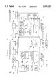
- FIGS. 1 to 3 show three different hardware configurations of computer systems embodying the invention.
- a host computer 10 has its own backplane in the form of a VME bus 12 which provides general purpose communications between various circuit boards of the computer, such as processor, memory and disk controller boards.
- VME bus 12 which provides general purpose communications between various circuit boards of the computer, such as processor, memory and disk controller boards.
- a renderer 16 and a video processor 18, a Futurebus+ 20, and a front-end board 22 is added to the renderer 16 and a video processor 18, a Futurebus+ 20, and a front-end board 22.
- the renderer 16 is connected to the VME bus 12 and the Futurebus+ 20, and also communicates with the video processor 18, which in turn drives an external colour monitor 24 having a high-resolution of, for example, 1280 ⁇ 1024 pixels.
- the front-end board 22 is also connected to the Futurebus+ 20 and can communicate with a selection of peripherals, which are illustrated collectively by the block 26.
- the configuration of FIG. 1 is of use when the host computer 10 has a VME backplane 12 and there is sufficient room in the computer housing 14 for the renderer 16, video processor 18, Futurebus+ 20 and front-end board 22, and may be used, for example, with a ⁇ Sun Workstation ⁇ .
- FIG. 2 In the case where the computer housing 14 is physically too small, or where the host computer 10 does not have a VME or Futurebus+ backplane, the configuration of FIG. 2 may be employed.
- a separate housing 28 is used for the renderer 16, video processor 18, front-end board 22 and Futurebus+ 20, as described above, together with a VME bus 12 and a remote interface 30.
- a host interface 32 is connected to the backplane 34 of the host computer 10, which may be of VME, Qbus, Sbus, Multibus II, MCA, PC/AT, etc. format.
- the host interface 32 and remote interface 30 are connected by an asynchronous differential bus 36 which provides reliable communication despite the physical separation of the host and remote interfaces.
- the configuration of FIG. 2 is appropriate when the host computer 10 is, for example, an ⁇ Apple Mackintosh ⁇ , ⁇ Sun Sparkstation ⁇ , ⁇ IBM-PC ⁇ , or Du Pont Pixel Systems bRISC'.
- FIG. 3 In the event that a host computer becomes available which has a Futurebus+ backplane and sufficient space in its housing for the additional components, then the configuration of FIG. 3 may be employed. In FIG. 3, the renderer 16 and the front-end board 22 are directly connected to the Futurebus+ backplane 20.
- the host computer 10 supplies data in the form of control information, high level commands and parameters therefor to the renderer 16 via the VME backplane (FIG. 1), via the backplane 34, host and remote interfaces 32, 30 and the VME bus 12 (FIG. 2), or via the Futurebus+ backplane 20 (FIG. 3). Some of this data may be forwarded to the front-end board via the Futurebus+ 20 (FIGS. 1 and 2), or sent direct via the Futurebus+ backplane 20 (FIG. 3) to the front-end board 22.
- the Futurebus+ 20 serves to communicate between the renderer 16 and the front-end processor 22 and is used, in preference to a VME bus or the like, in view of its high bit width of 128 bits and its high bandwidth of about 500 to 800 Mbytes/s.
- the renderer 16 includes an image memory, part of which is mapped to the monitor 24 by the video processor 18, and the renderer serves to perform image calculations and rendering, that is the drawing of polygons in the memory, in accordance with the commands and parameter supplied by the host computer 10 or the front-end board 22.
- the front-end board 22 serves a number of functions. It includes a large paging RAM, which also interfaces with external disk storage, to provide a massive paging memory, and pages of image data can be swapped between the paging RAM and the image memory of the renderer 16 via the Futurebus+ 20.
- the front-end board also has a powerful floating-point processing section which can be used for graphics transformation and shading operations. Furthermore, the front-end board may provide interfacing with peripherals such as a video camera or recorder, monitor, MIDI audio, microphone, SCSI disk and RS 232.
- the renderer 16, video processor 18 and front-end board 22 can accelerate pixel handling aspects of an application, and also accelerate other computation intensive aspects of an application.
- the renderer 16 and video processor 18 will now be described in greater detail with reference to FIG. 4, which shows the main elements of the renderer 16 and the main data and address pathways.
- the renderer 16 includes a 32-bit internal bus 300, a VME interface 301 which interfaces between the VME bus 12 (FIG. 1) or the remote interface 30 (FIG. 2) and the internal bus 300, and a Futurebus+ interface 302 which interfaces between the Futurebus+ 20 and the internal bus 300. Also connecting to the internal bus 300 are a control processor 314 implemented by an Intel 80960i, an EPROM 303, 4 or 16 Mbyte of DRAM 304, a real time clock and an I/O block 306 including a SCSI ports.
- a control processor 314 implemented by an Intel 80960i, an EPROM 303, 4 or 16 Mbyte of DRAM 304, a real time clock and an I/O block 306 including a SCSI ports.
- control processor 314 and the associated DRAM 304 and EPROM 303 are (a) to boot-up and configure the system; (b) to provide resource allocation for local PRAM 318, 322 of address and grid processors 310, 312 (described in detail below) to ensure that there is no memory space collision; (c) to control the leading of microcode into microcode memories 307, 308 (described below); (d) to run application specific remote procedure calls (RPCs); and (e) to communicate via the I/O block 306 with a diagnostics port of the host computer 10 to enable diagnostics information to be displayed on the monitor 24.
- the DRAM 304 can also be used as a secondary image page store for the VRAM 700 described below.
- the renderer 16 also includes an address processing section 309 comprising an address broadcast bus 311 to which are connected 64 kbyte of global GRAM 316, a data/instruction cache 313 which also connects to the internal bus 300, an internal bus address generator 315 which also connects to the internal bus 300, an address processor 310 with 16 kbyte of local PRAM 318, and a sequencer 317 for the address processor 310 which receives microcode from a microcode memory 307.
- the address processor 310 also connects to a virtual address bus 319.
- the main purpose of the address processing section 309 is to generate virtual addresses which are placed on the virtual address bus under control of microcode from the microcode memory 307.
- an address translator 740 (described in further detail below) which receives the virtual addresses on the virtual address bus 319 and translates them into physical addresses of data in the video RAM 700, if the required data is present, or interrupts the address processor 310 to cause the required data to be swapped in from the paging RAM 304 or other page stores on the external buses, if the required data is not present in the VRAM 700.
- the renderer 16 furthermore includes a data processing section 321 which is somewhat similar to the address processing section 309 and comprises a data broadcast bus 323, to which are connected 64 kbyte of global GRAM 324, a diagnostics register 325 which also connects to the internal bus 300 and which may be used instead of the I/O block 306 to send diagnostics information to the host computer 10, an internal bus address generator 327 which also connects to the internal bus 300, a grid processor 312 having sixteen processors each with 8 kbyte of local PRAM 322, and a sequencer 329 for the grid processor 312 which receives microcode from a microcode memory 308.
- the processors of the grid processor 312 also connect to a data bus 331.
- the main purpose of the data processing section 321 is to receive data on the data bus 331, process the data under control of microcode from the microcode memory 308, and to put the processed data back onto the data bus 331.
- the physical VRAM 700 connects with the data bus 331 via an exchange 326 which is described in detail below, but which has the main purposes of shuffling the order of the sixteen pixels read from or written to the VRAM 700 at one time, as desired, to enable any of the sixteen processors in the grid processor 312 to read from or write to any of the sixteen addressed locations in the VRAM 700 and to enable any of the sixteen processors to transfer pixel data to any other of the sixteen processors.
- the last main element of the renderer 16 is a bidirectional FIFO 332 connecting between the broadcast buses 311, 323 of the address and data processing sections 309, 321, which enables virtual addresses to be transferred directly between these two sections.
- the front-end board 22 will now be described in greater detail with reference to FIG. 5.
- the front-end board 22 has an internal bus 502 which communicates with the Futurebus+ 20.
- a paging memory section 504 is connected to the internal bus 502 and comprises a large paging RAM 506 of, for example, 4 to 256 Mbytes capacity which can be used in conjunction with the DRAM 304 of the renderer, a paging memory control processor 508, and connections to, for example, two external high speed IPI-2 disk drives 510 (one of which is shown) each of which may have a capacity of, for example, 4 Gbytes, and a data communication speed of 50 Mbytes/s, or two external SCSI drives.
- the paging RAM 506 enables an extremely large amount of pixel data to be stored and to be available to be paged into the renderer 32 as required, and the fast disk 510 enables even more pixel data to be available ready to be transferred into the paging RAM 506.
- Floating point processing is provided by 1 to 4 Intel 80860 processors 516, each rated at 80 MFlops peak.
- the general purpose processing power can be used on dedicated tasks such as geometric pipeline processing, or to accelerate any part of an application which is compute-intensive, such as floating point fast Fourier transforms.
- Each of the floating point processors 516 has a 128 KByte secondary cache memory 518 in addition to its own internal primary cache memory.
- the front-end board 22 may also, if desired, include a broadcast standard 24-bit frame grabber connected to the internal bus 502 and having a video input 514 and output 516 for connection to video camera or television-type monitor.
- the front-end board 22 may also, if desired, include an input/output processor 520 which provides interfacing with MIDI on line 522, SCSI disk on line 524, at least one mouse on line 526, RS232 on line 528, and audio signals on line 530 via a bi-directional digital/analogue convertor 532.
- an input/output processor 520 which provides interfacing with MIDI on line 522, SCSI disk on line 524, at least one mouse on line 526, RS232 on line 528, and audio signals on line 530 via a bi-directional digital/analogue convertor 532.
- the VRAM has a of 16 Mbyte capacity.
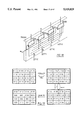
- pixels are arranged in 4 ⁇ 4 groups referred to as ⁇ patches ⁇ .
- FIGS. 6A and 6B show, respectively, two-and one-dimensional notations for designating a pixel in a patch, as will be used in the following description.
- the patches are arranged in 32 ⁇ 32 groups referred to as ⁇ pages ⁇ .
- the pages are arranged in 4 ⁇ 4 groups referred to as superpages.
- the VRAM therefore has a capacity of 4 Mpixels, or 256 k patches, or 256 complete pages, or 16 complete superpages.
- not all pages of a particular superpage need be stored in the memory at any one time, and support is provided for pages from parts of up to 128 different superpages to be stored in the physical memory at the same time.
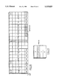
- Each small cube 702 in FIG. 8 represents a 32-bit pixel.
- the pixels are arranged in 512 pixel ⁇ 512 pixel banks B(0)-B(15) lying in the XY plane, and these pixel banks are 16 pixels deep (in the P direction).
- a line of 16 pixels in the P direction provides an aligned patch 704.
- the pixels in each bank are addressable as to X address by a respective one of 16 9-bit X address lines AX(0) to AX(15) and are addressable as to Y address by a respective one of 16 9-bit Y address lines AY(0) to AY(15).
- the Y and X addresses are sequentially supplied on a common set of 16 9-bit address lines A(0) to A(15), with the Y addresses being supplied first and latched in a set of 16 9-bit Y latch groups 706-0 to 706-15 each receiving a row address strobe (RAS) signal on 1-bit line 708, and the X addresses then being supplied and latched in a set of 16 9-bit X latch groups, 707-0 to 707-15 each receiving a respective column address strobe signal CAS(0) to CAS(15) on lines 709(0) to 709(15), respectively.
- RAS row address strobe
- Each Y latch group and X latch group comprises eight latches (shown in detail for Y latch group 706(1) and X latch group 707(1) and a respective one of the X and Y latches is provided on each VRAM chip 710.
- the banks of memory will sometimes be referred to by the bank number B(0) to B(15) and at other times by a 2-dimensional bank address (bx,by) with the correlation between the two being as follows:
- a patch of 16 pixels is made available for reading or writing at one time. If the Y address and X address for all of the VRAMs 710 is the same, then an "aligned" patch of pixels (such as patch 704) will be accessed. However, it is desirable that access can be made to patches of sixteen pixels which are not aligned, but where various pixels in the patch to be accessed are derived from two or four adjacent aligned patches.
- a further problem which arises in accessing a non-aligned patch "p" is that the (x,y) address of each pixel in the patch "p" does not correspond to the bank address (bx,by)in the memory from which that pixel is derived.
- the following pixel derivations and translations are required.
- the translation from the bank address (bx,by) to the corresponding address in the non-aligned patch is constant for a particular non-aligned patch and in particular is equal to the negative of the misalignment (mx,my) of the non-aligned patch "p" from the base aligned patch "a", all translations being in modulus arithmetic with the modulus equal to the patch dimension.
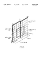
- FIG. 11A represents four contiguous pages A, B, C, D in the virtual address space.
- these pages may be scattered at, for example, page addresses (8,6), (4,8), (12, 12) and (6,10) in the VRAM, as represented in FIG. 11B.
- page addresses (8,6), (4,8), (12, 12) and (6,10) in the VRAM as represented in FIG. 11B.
- the non-aligned patch "p" may extend into page B, page C or pages B, C and D, depending on the direction of the misalignment.
- FIG. 11A represents four contiguous pages A, B, C, D in the virtual address space.
- the following table sets out, for each of the pixels in the patch "p" to be accessed: the page and patch address of the aligned patch from which that pixel is derived; the translation necessary from the patch address of the basic patch "a" in page A to the patch address of the patch from which the pixel is derived; the bank address from which the pixel is derived; and the translation necessary from this latter address to the address of the pixel in the patch "p".
- FIG. 11C A representation of the locations of the pixels in the four aligned patches is shown in FIG. 11C.
- the basic patch "a” has a patch address (px,py) of (31,31) and the non-aligned patch “p” to be accessed has a misalignment (mx, my) of (2,1) relative to the basic patch "a".
- the VRAM 700 is addressed by the address processor 310 via the address translator 740 communicates data with the grid processor 312 via the exchange 326 and provides data to the video processor 34.
- a greater degree of detail of the address translator, VRAM and exchange is shown in FIG. 14.
- the address translator 740 receives a 48-bit virtual address on bus 319 of a patch origin address. The translator determines whether the required page(s) to access the addressed patch are resident in the VRAM physical memory 700. If not, a page or superpage fault is flagged on line 748, as will be described in detail below, However, if so, the address translator determines the addresses in the sixteen XY banks of the physical memory of the sixteen pixels making up the patch, and addresses the memory 700 firstly with the Y addresses on the sixteen sets of 9-bit lines A(0) to A(15) and then with the X addresses on these lines. The X and Y addresses are generated under control of the X/Y select signal on line 713.
- the exchange 326 includes a read surface shifter 742 and a write surface shifter 744. Pixel data is transferred, during a read operation, from the memory 700 to the read surface shifter 742 by a set of sixteen 32-bit data lines D"(0) to D"(15), and, during a write operation, from the write surface shifter 744 to the memory 700 by the same data lines D"(0) to D"(15).
- the read and write surface shifters 742, 744 receive 4-bit address data from the address translator on line 770, consisting of the least significant two bits of the X and Y address data. This data represents the misalignment (mx, my) of the accessed patch "p" from the basic aligned patch "a".
- the purpose of the surface shifters is re-order the pixel data in non-aligned patches, that is to apply the translation (-mx, -my) when reading and an opposite translation (mx, my) when writing.
- Pixel data to be written is supplied by a crossbar 327 forming part of the exchange 326 to the write surface shifter 744, and pixel data which has been read is supplied by the read surface shifter 742 to the crossbar 327, on the 512-bit line 750 made up of a set of 16 32-bit lines.
- the write surface shifter also receives on line 745 16-bit write enable signals WE(0)-WE(15) from the crossbar 327 one for each pixel, and the write surface shifter 744 re-organises these signals in accordance with the misalignment (mx, my) of the patch "p" to be accessed to provide the sixteen column write enable signals WE"(0) to WE"(15). Each of these signals is then ANDed with a common CAS signal on line 709 to form sixteen CAS signals CAS(0) to CAS(15), one for each of the sixteen banks of memory. This enables masking of pixels within a patch during writing, taking into account any misalignment of the patch.
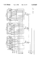
- the address translator 740 will now be described in more detail primarily with reference to FIG. 15.
- the translator 740 includes as shown, a contents addressable memory (CAM) 754, a page address table 756, a near-page-edge table 758, and X and Y incrementers 760X, 760Y.
- the translator 740 also includes sixteen sections 764(0) to 764(15), one for each output address line A(0) to A(15), and thus for each memory bank B(0) to B(15).
- the translator 740 receives a 48-bit virtual address of the origin (0,0) pixel of a patch on the bus 319. It will therefore be appreciated that up to 2 48 (i.e. 281, 474, 976, 710, 656) different pixels can be addressed. Many formats of the 48-bit address can be employed, but the following example will be considered in detail.
- the bits identifying the superpage are supplied to the CAM 754.
- the CAM 754 is an associative memory device which compares the incoming 30-bit word with all of the words held in its memory array, and if a match occurs it outputs the location or address in the memory of the matching value on line 767.
- the CAM 754 has a capacity of 128 32-bit words. Thirty of these bits are used to store the virtual address of a superpage which is registered in the CAM 754. Thus up to 128 superpages can be registered in the CAM. One of the other bits is used to flag any location in the CAM which is unused. The remaining bit is spare.
- FIG. 16 illustrates how the CAM 754 operates.
- this input value is compared with each of the contents of the CAM. If a match is found and provided the unused flag is not set, the address in the CAM of the match is output, e.g. 1 in the illustration. If no match is found with the contents at any of the 128 addresses of the CAM, then a superpage fault is flagged on line 748S, and the required superpage is then set up in the CAM in the manner described in detail later.
- the 7-bit superpage identification output from the CAM 754 on line 767 is used as part of an address for the page address table 756, implemented by a 4 k word ⁇ 16-bit SRAM.
- the remaining 5 bits of the address for the page table 756 are made up by: bits 7, 8, 23 and 24 of the virtual address which identify the page within a superpage; and an X/Y select signal on line 713.
- the page table 756 has registered therein the X and Y page addresses in the VRAM 700 of: a) the basic page A in which the pixel to be accessed is located; b) the page B which is to the right of the page A in the virtual address space; c) the page C which is above the page A in the virtual address space; and d) the page D which is to the right of page C and above page B in the virtual address space, and these addresses are output on lines 771A to 771D, respectively. If these pages A to D are required, but are not stored in the VRAM 700 and thus are not registered in the page table 756, then a page fault is flagged on a line 748p (as described below with reference to FIG.
- Bits 2 to 6 and 18 to 22 of the virtual address are also supplied to each of the sections 764(0) to 764(15) on lines 772X and 772Y. These denote the patch address (px, py).
- the X and Y patch addresses together with bits 0,1, 16 and 17 of the virtual address (which indicate the misalignment mx, my of the patch p to be accessed) are also supplied to the near-page-edge table 758, implemented using combinatorial logic, which provides a 2-bit output to the sections 764(0) to 764(15) on line 774, with one bit being high only if the patch X address px is 31 and the X misalignment mx is greater than zero and the other bit being high only if the patch Y address py is 31 and the Y misalignment my is greater than zero.
- the X and Y patch addresses (px, py) are also supplied to the X and Y incrementers 760X, 760Y, and these incrementers supply the incremented values px+1, mod 32 and py+1, mod 32, to each of the sections 764(0) to 764(15) on lines 776X, 776Y.
- the four bits 0,1, 16 and 17 giving the misalignment mx and my are also supplied to the sections 764(0) to 764(15) on lines 770X, 770Y and are also supplied to the surface shifters 742, 744 on line 770.
- Each section 764(0) to 764(15) comprises: a page selection logic circuit 778; X and Y increment select logic circuits 780X 780Y; X and Y 4:1 4-bit page address multiplexers 782X, 782Y; X and Y 2:1 5-bit patch address multiplexers 784X, 784Y; and a 2:1 9-bit address selection multiplexer 786.
- the page selection logic circuit 778 implemented using combinatorial logic, provides a 2-bit signal to the page address multiplexers 782X,Y to control which page address A, B, C or D to use.
- the page selection logic circuit 778 performs this selection by being configured to act as a truth table which corresponds to the table of FIG. 12.
- the circuit 778 receives the 2-bit signal on line 774 from the near-page-edge table 758 and this determines which of the four columns of the table of FIG. 12 to use.
- the circuit 778 also receives the misalignment (mx, my) on lines 770X, 770Y, and this data in combination with which section 764(0) to 764(15) (and thus which bx and by applies) determines which of the four rows in FIG. 12 to use.
- the X and Y page address multiplexers 782X, 782Y therefore supply appropriate page address as four bits to complementary inputs of the X/Y address selection multiplexer 786.
- the increment selection logic circuits 780X, 780Y which are implemented using combinatorial logic, receive the respective X and Y misalignments mx, my and provide respective 1-bit signals to control the patch address multiplexers 784X, 784Y.
- the increment selection circuits perform this selection by being configured to act as truth tables which correspond to the upper and lower parts, respectively, of the table of FIG. 13. It will be noted that selection depends upon the misalignment mx or my in combination with the bx or by position of the memory bank (and thus which of the sections 764(0) to 764(15)is being considered).
- the X and Y patch address multiplexers 784X, 784Y therefore output the appropriate 5-bit patch addresses px or px+1 (mod.
- This latter multiplexer receives as its control signal the X/Y selection signal on line 713 and therefore outputs the 9-bit X or Y address appropriate to the particular section 764(0) to 764(15).
- the address translator 740 therefore deals with the problems described above of addressing pixels from different aligned patches a, b, c, d in the memory 700 when a patch "p" to be accessed is misaligned, and of addressing pixels from different pages A, B, C, D in the memory 700 when a patch "p" to be accessed extends across the boundary of the basic page A.
- the read surface shifter 742 comprises a pair of 4 ⁇ 4 32-bit barrel shifters, 788X, 788Y.
- the X barrel shifter 788X has four banks 790X(0) to 790X(3) of multiplexers arranged in one direction, and the outputs of the X barrel shifter 788X are connected to the inputs of the Y barrel shifter 788Y, which has four banks 790Y(0) to 790Y(3) of multiplexers arranged in the orthogonal direction.
- the X and Y barrel shifters 788X, Y receive the X and Y misalignments mx, my, respectively.
- One of the banks of muliplexers 790X(0) is shown in greater detail in FIG. 18, and comprises four 32-bit 4:1 multiplexers 792(0) to 792(3).
- the data from bank (0,0) is supplied to inputs 0, 3, 2 and 1, respectively, of the multiplexers 792(0) to 792(3).
- the data from bank (1,0) is supplied to inputs 1, 0, 3 and 2, respectively, of the multiplexers 792(0) to 792(3).
- the data from bank (2,0) is supplied to the inputs 2, 1, 0 and 3, respectively, of the multiplexers 792(0) and 792(3).
- the remaining data from bank (3,0) is supplied to the remaining inputs 3, 2, 1, 0, respectively, of the multiplexers 792(0) to 792(3).
- the other banks of multiplexers 790X(1) to 790X(3) in the X barrel shifter 788X are similarly connected, and the banks 790Y(0) to 790Y(3) in the Y barrel shifter 788Y are also similarly connected. It will therefore be appreciated that the read surface shifter performs a translation with wrap-around in the -X direction of mx positions and a translation with wrap-around in the -Y direction of my positions as shown in FIG. 19.
- the write surface shifter 744 may be provided by a separate circuit to the read surface shifter.
- the write surface shifter is configured similarly to the read surface shifter, except that the inputs 1 and 3 to the multiplexers 792 in the barrel shifter banks are transposed. This results in translations of +mx and +my in the X and Y directions, rather than -mx and -my for the read surface shifter.
- the part of the write surface shifter which operates on the write enable signals WE(0) to WE(15) is identical to the part which operates on the data signals, except that the signals are 1-bit, rather than 32-bit.
- a single circuit may be employed, with appropriate data routing switches, and in this case translation provided by the surface shifter may be switched between (-mx, -my) and (+mx, +my), in dependence upon whether the memory is being read or written, as described with reference to FIGS. 46 and 47.
- a superpage fault is flagged, on line 748S.
- This superpage fault is used to interrupt the address processor 310, which is programmed to perform a superpage interrupt routine as follows. Firstly, the address processor checks whether the CAM 754 has any space available for a new superpage to be registered. If not, the address processor selects a registered superpage which is to be abandoned in the manner described below and causes the, or each, page of that superpage which is stored in the VRAM 700 to be copied to its appropriate location in the paging memory. The registration of that superpage is then cancelled from the CAM 754. Secondly, the new superpage is registered in the CAM 754 at the, or one of the, available locations.
- LRU least recently used
- a 128 ⁇ 16-bit LRU table 802 is provided, as illustrated in FIG. 20.
- Each of the 128 addresses represents a respective one of the superpages registered in the CAM 754.
- the 7-bit superpage identification output from the CAM 754, on line 767 is used to address the LRU table 802 each time the superpage identification changes, as detected by the change detector 804.
- the change detector 804 also serves to increment a 16-bit counter 806, and the content of the counter 806 is written to the addressed location in the LRU table 802.
- the LRU table contains an indication of the order in which those superpages were last used.
- the address processor 310 checks the contents of the LRU table 802 to determine which superpage has the lowest count and in that way decides which superpage to abandon.
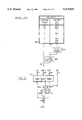
- the page fault generator is shown in FIG. 21, and comprises a page fault table 794 constituted by a 2 k ⁇ 4-bit SRAM, a set of three AND gates 796B, C, D and an OR gate 798.
- the page fault table 794 is addressed by the 7-bit superpage identity code on line 767, and by the X and Y page addresses on fine 768X, Y.
- the page fault table 794 contains a 4-bit flag in which the bits denote whether the basic addressed page A and the pages B, C and D, respectively, to the right, above, and to the right and above, page A are stored in the VRAM 700.
- the page B flag is ANDed by gate 796B with the bit of the near-page-edge signal on line 774 denoting whether the patch "p" to be accessed extends across the boundary between pages A and B.
- the page C flag is ANDed by gate 796C with the bit of the near-page-edge signal on line 774 denoting whether the patch "p" to be accessed extends across the boundary between pages A and C.
- the page D flag is ANDed by gate 796D with both bits of the near-page-edge signal, which in combination denote whether the patch "p" to be accessed extends in page D above page B and to the right of page C.
- the outputs of the three AND gate 796B, C, D and the page A flag are then ORed by the OR gate 798, the output of which provides the page fault flag on line 748P.
- the page fault signal on line 748P is used to interrupt the address processor 310.
- the address processor searches a table in its PRAM 318 for a spare page address in the VRAM 700, causes the required page to be swapped into the VRAM at the spare page address, and update the table in its PRAM 318.
- the exchange 326 and the VRAM 700 communicate in patches of sixteen pixels of data, each pixel having 32 bits.
- the grid processor 312 has sixteen processors, each of which processes pixel data and communicates with the exchange 326. Also, the grid processor 312 and the address processor 310 can communicate address data via the FIFO 332.
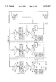
- the exchange 326 includes a crossbar 377, and a logical implementation of the crossbar 377 and of the grid processor 312 is shown in more detail in FIG. 22.
- the crossbar 377 comprises sixteen 16:1 32-bit data multiplexers 602(0) to 602(15); sixteen 16:1 1-bit write enable multiplexers 603(0) to 603(15); a 512-bit bidirectional FIFO 604 for pixel data; and a 16-bit bidirectional FIFO 605 for the write enable signals.
- the 16 pixels of a 4 ⁇ 4 patch are supplied from the VRAM 700 (FIG.
- the data multiplexers 602(0) to 602(15) supply data D(0) to D(15) via the FIFO 604 and the write surface shifter 744 to the VRAM and the write enable multiplexers 603(0) to 603(15) supply write enable signals WE(0) to WE(15) via the FIFO 605 to the write surface shifter 744.
- the FIFOs 604, 605 and also the FIFO 332 are employed so that the grid processor 312 does not need to be stalled to take account of different access speeds of the VRAM 700 in dependence upon whether page-mode of non-page-mode access is taking place.
- Each of the data multiplexers 602(0) to 602 (15)is associated with a respective one of sixteen processors 606(0) to 605(15) and communicates therewith respective data signals D'(0) to D'(15), which are logically 32 bits, but which in practice may be implemented physically as 16 bits, with appropriate multiplexing techniques.
- the data signals D'(0) to D'(15) are also supplied to respective parts of the bus 331.
- each of the write enable multiplexers 603(0) to 603(15) is associated with a respective one of the sixteen processors 606(0) to 606(15) to 606(15)which supply respective 1-bit write enable signals WE'(0) to WE'(15) to the write enable multiplexers.
- Each processor 606(0) to 606(15) provides a logical control signal CO(0) to CO(15) to control both its associated data multiplexer 602 and write enable multiplexer 603.
- any processor may provide any respective one of the data signals by providing the number 0 to 15 of the required data signal as its control signal to its data and write enable multiplexers.
- any processor may read any of the data signals by providing the number 0 to 15 of the required data signal to its data multiplexer.
- the crossbar 377 shown in FIG. 22 is simplified for reasons of clarity, and shows, for example, hi-directional multiplexers, which in practice are difficult to implement.
- a modified form of the exchange, incorporating the crossbar and the surface shifters, is shown in FIG. 46.
- the exchange of FIG. 46 comprises sixteen sections, of which one typical section 326(i) is shown for simplicity.
- the data D"(i) from the memory is supplied via a buffer BA(i) and register RA(i) to one input of a 2.1 multiplexer SA(i) acting as a two-way switch.
- the output of the switch SA(i) is fed to an input i of the surface shifter 743 which performs surface shifting for read and for write.
- the corresponding output i of the surface shifter 743 is fed to one input of a multiplexer switch SB(i) and is also fed back to the data D"(i) input via a register RB(i) and a tri-state buffer BB(i).
- the output of the switch SB(i) is input to a FIFO(i), the output of which forms the other input of switch SA(i) and is also fed to one input of a further switch SC(i).
- the set of sixteen data lines D(0) to D(15) connect the exchange sections 326(0) to 326(15) and the output of switch SC(i) is connected to data line D(i).
- the output of each switch SC(0) to SC(15) is connected to the data line of the same number.
- the sixteen inputs of a 16:1 multiplexer MUX(i) are connected to the data lines D(0) to D(15), and the output of the multiplexer MUX(i) is connected via a register RC(i) and a tri-state buffer BC(i) to the respective processor PROC(i) via the data line D'(i).
- the output of the multiplexer MUX(i) is also connected to the other input of switch SB(i).
- the data line D'(i) from the processor PROC(i) is also connected via a buffer BD(i) and a register RD(i) to the other input of the switch SC(i).
- the control signal CO(i) for the multiplexer MUX(i) is provided by a switch SD(i) which can select between a hardwired value i or the output of a register RE(i) which receives its input from the output of the register RD(i).
- control signals CSB, CSC, CSD and CBC are supplied to the multiplexer switches SB(0) to (15), the multiplexer switches SC(0) to (15), the multiplexer switches SD(0) to SD(15), the tri-state buffers BC(0) to (15) from the microcode memory 308 (FIG. 4) of the processing section 321.
- control signals CSA, CBB and CSS derived from the microcode memory 307 of the address processing section 309 are supplied to the multiplexer switches SA(0) to (15), the tristate buffers BB(0) to (15) and the surface shifter 743.
- the exchange 326 of FIG. 46 is operable in three modes.
- the processors PROC(0) to PROC(15) can read the memory; in a write mode, they can write to the memory; and in a transfer mode, they can transfer pixel data between each other.
- the values of the control signals for these three modes are as follows:
- control signal CSD can select between a "straight-through” mode in which each multiplexer MUX(i) selects its input i and thus data D(i), or a "processor-selection” mode in which it selects an input j and thus data D(j) in accordance with the value j which the processor has loaded into the register RE(i).
- FIG. 47A The effective configuration of a generalised one of the exchange sections 326(i) of FIG. 46 in the read mode is shown in FIG. 47A.
- the data path from the data line D"(i) is via the register RA(i) to the surface shifter 743.
- the surface shifter applies a shift of (-mx,-my) (mod. 4) to the data paths.
- the data path continues via the FIFO(i) to the data line D(i).
- the output data passes via the register RC(i) as data D'(i) to the processor PROC(i).
- the effective configuration of the exchange section 326(i) in the write mode is shown in FIG. 47B.
- the data D'(i) from the respective processor PROC(i) passes via the register RD(i) to the data line D(i).
- the output data passes via the FIFO(i) to the surface shifter 743.
- the surface shifter applies a shift (+mx,+my) (mod. 4) to the data paths. From the surface shifter, the data path continues via the register RB(i) as data D"(i) to the VRAM 700.
- the write-enable signal follows the same path WE'(i) to WE(i) to WE"(i) as the data signal path D'(i) to D(i) to D"(i).
- these paths are logically 33 bits made up from 32 bits for the data signal and 1 bit for the write-enable signal.
- the effective configuration of the exchange section 326(i) is as shown in FIG. 47C.
- the control signal CSD to the switch SD(i) is set to 1 so that the multiplexer MUX(i) receives as its control signal the value j loaded into the register RE(i).
- the processors output the values j of the data D(j) which they wish to receive as the lowest four bits of their data lines, and these values j are clocked into the registers RD(i).
- the processors In the second phase, the processors output the data to be transferred out, and this data is clocked into the registers RD(i), while the values j are clocked out of the registers RD(i) and into the registers RE(i), thus setting the multiplexers MUX(i) to receive the data on the respectively selected lines D(j).
- the data in the registers RD(i) is clocked out onto the lines D and each multiplexer MUX(i) receives and outputs the data on respectively selected line D(j).
- the outputs of the multiplexers are clocked into the registers RC(i) and the tristate buffers BC(i) are enabled so that the processors can transfer in the data from the buffers BC(i).
- each processor PROC(i) receives the data (j) from the processor PROC(j) which was selected by the processor PROC(i) by its output value j in the first phase.
- the processors 606(0) are connected to the data broadcast bus 323 and to a priority encoder 614, having 16 sections and which is associated with the sequencer 329.
- the processors 606(0) to 606(15) communicate address data with the data broadcast bus 323 and the FIFO 332 connects the data broadcast bus 323 with the address processor 310.
- the processors 606(0) to 606(15) can also supply respective "unsatisfied" signals US(0) to US(15) and respective "X waiting" signals XW(0) to XW(15) to the respective sections of the priority encoder and can receive respective "process enable" signals EN(0) to EN(15) from the respective sections of the priority encoder 614.
- the priority encoder 614 has a sequencer enable (SE) output on line 618 to the sequencer 329 which controls the sequence of processing of a series of microcode instructions by the processors 606.
- SE sequencer enable
- the purpose of the priority encoder 614 is to provide high efficiency in the accessing by the processors 606 of the memory 700.
- the encoder 614 and processors perform the following process, which is shown in the flow diagram of FIG. 23.
- the left-hand three columns contain steps which are taken by the processors 606(0) . . . 606(i) . . . 606(15), or PROC(0) . . . PROC(i) . . . PROC(15), in parallel with each other, the right-hand column contains steps performed by the priority encoder.
- steps 620 to 628 there are a series of initialisation steps 620 to 628.
- steps 620 to 625 those processors which require access to the memory set (1) their respective unsatified signals US and reset (0) their X waiting signals XW, and those processors which do not require access reset (0) their unsatisfied signals US and their X waiting signals XW.
- steps 626, 628 the priority encoder resets (0) the process enable signals EN for all of the processors and also resets (0) the sequencer enable signal SE.
- the priority encoder 614 checks through the XW signals, starting with XW(0) in step 630 to find any processor which is X waiting, and if a match is found (step 632) at a processor, designated PROC(q), then the routine proceeds to step 640. If a match is not found, however, in step 632, then the priority encoder checks through the US signals, starting with US(0) in step 634 to find a processor which is unsatisfied, and if a match is found (step 636) for a processor, designated PROC(q), then the routine proceeds to step 640. If a match is not found, however, in step 636, then this indicates that all processors are satisfied, and accordingly the microcode program can proceed. Therefore, the sequence enable signal SE is set in step 638, and the routine terminates.
- step 640 the process enable signal EN(q) for the selected processor PROC(q) is set.
- each processor determines whether it is unsatisfied, and if not exits the subroutine of steps 642 to 654. For any processor which is unsatisfied, then in steps 644, that processor determines whether it is the selected processor, and if so supplies, in step 645, to the data broadcast bus 323 as (xq, yq) the virtual address of the base pixel (0,0) of the patch of pixel data which it wishes to process. This address is supplied via the FIFO 332 to the address processor 310, which in response accesses the appropriate locations in the memory 700, swapping in and out pages of pixel data, if required, as described above.
- step 656 the priority encoder resets (0) the process enable signal EN(q) for the selected processor.
- the routine then loops back to step 630.
- PROC(0) to (3) and (8) to (11) require access to the patches having the base pixel X and Y addresses listed in column 660 of the table, the addresses being in hexadecimal notation.
- US(0) to (3) and (8) to (11) are set to 1 and the other US signals and the XW signals are reset to 0, as shown in column 662.
- processors which require access to the same patch can access that patch simultaneously. Furthermore, when a plurality of processors require access to different patches having the same Y address, their accesses are made immediately one after the other, in "page mode". Therefore the address translator does not need to re-latch the Y address(es) in the Y address latches 706(0) to (15) (FIGS. 8 and 14) between such accesses. Thus, a considerable improvement in performance is achieved as compared with a case where the processors PROC(0) to (15) access their required patches one at a time, sequentially and without reference to any similarity between the addresses to be accessed.
- up to sixteen pixels in a patch are processed in parallel by sixteen processors.
- the system is also arranged so that a group of patches, for example, up to 32 patches, are processed in series in order to reduce pipeline start and finish overheads.
- the method of operation may be modified, as compared with that shown in FIG. 23, in order to increase efficiency, by permitting any processor requiring access to, say, a jth pixel in the group to request that pixel without firstly waiting for all the other processors to complete access to their (j-1)th pixels in the group. To do this, between steps 623 and 630 in FIG.
- step "set address of first required pixel in group as (xi, yi)" is included for each processor PROC(i). Furthermore, steps 650 and 652 for each processor as shown in FIG. 23 are replaced by the steps shown in FIG. 48.
- step 682 the memory is accessed at address xi, yi for the particular processor PROC(i). Then, in step 684, it is determined whether or not the processor PROC(i) requires access to a further pixel in the group, and if not in step 686, the unsatisfied flag US(i) and the X waiting flag XW(i) are both reset to 0, similarly to step 650 in FIG. 23.
- step 684 the processor PROC(i) sets the address of the next required pixel as (xi, yi). Then, in step 690, it is determined whether or not the new y address yi is equal to the Y address yq of the last accessed pixel. If so, then in step 692, the X waiting flag XW(i) is set to 1, whereas if not, then in step 694, the X waiting flag XW(i) is reset to 0. After steps 692 or 694, the routine proceeds to step 656 as in FIG. 23.
- a problem which can arise with the modification of FIG. 48 is that some of the processors can inordinately race ahead of others of the processors in accessing their thirty-two pixels. For example, in the case where the processors require access to many different Y addresses, it may arise that PROC(0) accesses all of its thirty-two required pixels first, then PROC(1) accesses its thirty-two pixels, and so on. In order to obviate this problem, the following further modification may be made. Basically, access is permitted with the following order of priority: (a) of highest priority, processors which require access in page-mode (i.e.
- the process of FIGS. 23 and 48 is then modified as follows.
- the additional steps are included of resetting to zero LP(i) and WM in the register files of all processors, and setting HP to the number of accesses in the series, usually 31.
- the step 642 in FIG. 23 is replaced by "LP(i) ⁇ >HP?".
- step 682 in FIG. 48 where a processor accesses the memory, it also increments it local pointer to LP(i)+1. This then has the affect of dealing with priorities "a" and "b" described above.
- the memory is capable of storing pixel data of 32 bits and that the grid processor is capable of processing pixel data logically of at least 32 bits.
- pixel data having a resolution as great as 32 bits is not needed, and all that may be required is 16-bit or 8-bit pixel data. In such cases it is possible to use only 16 or 8 bits of the 32 bits available for each pixel, but this would then result in the VRAM not being used to its full capacity, and pages of pixel data would need to be swapped between the VRAM and the paging memory more often than is necessary.
- the data is overlaid so that at no single address for each of the 128 VRAMs 710 does there exist data for more than one page. This is achieved by overlaying the 8- or 16-bit pixel data in units of a pixel, or more preferably units of a patch, as described below.
- FIG. 25 an aligned set of memory cells C(0) to C(127), one from each VRAM chip, and each 4 bits wide, is shown. In the 32-bit arrangement described above, these cells form an aligned patch of 4 ⁇ 4 pixels.
- L(0) is provided by C(0) to (3), C(8) to (11), C(16) to (19) . . . C(120) to (123).
- L(1) is provided by the remaining cells C(4) to (7), C(12) to (15), C(20) to (27) . . . C(124) to (127).
- layer L(0) is displayed immediately to the left of the layer L(1), as shown in FIG. 25.
- the cells form four layers L(0) to (3) of 16 pixel ⁇ 4 pixel patch.
- the layers are provided by the cells as follows:
- Layer L(0) C(0), C(1), C(8), C(9) . . . C(120), C(121)
- the layers are displayed left to right in the order L(0), L(1), L(2), L(3).
- the X patch address is, however, represented by bits 2-6 for 32-bit mode, by bits 3-7 for 16-bit mode, and by bits 4-8 for 8-bit mode. This makes available bit 2 in the 16-bit mode, and the two bits 2 and 3 in the 8-bit mode, to provide the level data, and leaves only one bit 8 in the 16-bit mode, and no bits in the 8-bit mode, for the X page address.
- FIGS. 26-29 The patch and page arrangements and the address notations used for them are represented in FIGS. 26-29.
- FIG. 26 shows the arrangement of patches in a single 16-bit page
- FIG. 27 shows the arrangement of 8 pages in one complete 16-bit superpage
- FIG. 28 shows the arrangement of patches in a single 8-bit page
- FIG. 29 shows the arrangement of 4 pages in one complete 8-bit superpage.
- the shift provided by the funnel shifter is controlled by a mode select signal MS on line 814 which is generated by a separate circuit in response to image header information provided prior to an image or graphics processing operation and which indicates whether the pixel data is 32-, 16- or 8-bit.
- the funnel shifter provides a page X address of up to two bits, a 5-bit patch X address, and the level data L of up to two bits.
- the relationship between the inputs to and outputs from the funnel shifter 812 is shown in the table of FIG. 31, and it will be noted that it corresponds to the required shifting derivable from the table set out above.
- the next complication arises due to the need to present the 16- or 8-bit pixels to the grid processor during reading such that the appropriate 16 or 8 bits of each pixel will be processed and not the remaining irrelevant 16 or 24 bits.
- This complication is overcome by supplying, during a read operation, all 32 bits from a location in the memory to the grid processor, together with shift data ZSFT in response to which the grid processor shifts the read pixel data by an amount corresponding to the ZSFT data, and then processes predetermined bits of the shift data, e.g. bits 0-15 for 16-bit processing, or bits 0-7 for 8-bit processing.
- the determination of the further aligned patch addresses b, c, d is performed by the patch x and y address multiplexers 784 X,Y and the patch y address increment select tables 780 Y described above with reference to FIG. 15 and by a modified form of the patch X address increment select table 780X which is responsive to the level data L and the mode select signal MS in addition to the X misalignment mx, as shown in FIG. 30B.
- the modified table 780X provides a 1-bit output to the X patch address multiplexer 784X in accordance with the truth table set out in FIG. 30C.
- the pixels labelled 6, 7, 10, 11, 14, 15, 2 and 3 require a ZSFT of 8 bits
- the pixels labelled 4, 5, 8, 9, 12, 13, 0 and 3, require a ZSFT of 16 bits.
- the circuit of FIG. 15 includes the addition shown in FIG. 34, in addition to being modified as described above with reference to FIGS. 30 and 31.
- the level value L and also the bits 0,1 of the ritual address for the misalignment mx are supplied as addresses to four ZSFT tables 818 a to d implemented using combinational logic.
- the ZSFT tables 818 also receive the mode select signal MS on line 814 and have three sections for 32-, 16- and 8-bit operation which are selected in dependence upon the MS signal.
- the ZSFT table 818a supplies the ZSFT values ZSFT(0), (4), (8), (12) corresponding to data D(0), (4), (8), (12) supplied from the read surface shifter 742 to the exchange 326;
- ZSFT table 818b supplies ZSFT (1), (5), (9), (15) for data D(1), (5), (9), (13);
- ZSFT table 818c supplies ZSFT (2), (6), (10), (14) for data D(2), (6), (10), (14);
- the table set out in FIG. 35A defines the values of ZSFT stored in the ZSFT tables 818a to d for different input misalignments mx, levels L and modes (8-, 16- or 32-bit) and in dependence upon the x value for the particular ZSFT table.
- the ZSFT values of 0, 1, 2, 3 represent a required shift of 0, 8, 16 and 24 bits respectively.
- the X near-page-edge signal no longer needs to be dependent solely upon whether or not 4 px+mx>124, but is also dependent upon the mode selected and the level data L.
- the modified table 758 of FIG. 36A produces X and Y values NPEx and NPEy of the 2-bit NPE signal as shown by the table set out in FIG. 36B.
- the modified arrangement is similar to the arrangement of FIG. 15 except in the following respects. Firstly, a 16 ⁇ 2-bit ZSFT FIFO 678 is provided to receive ZSFT(0) to (15).
- the output of the ZSFT FIFO 678 is supplied to each of sixteen 16:1 2-bit multiplexers 680(0) to 680(15).
- the 2-bit outputs of the ZSFT multiplexers 680(0) to 680(15) are supplied to the respective processors PROC(0) to PROC(15) as signals ZSFT'(0) to (15).
- the ZSFT muliplexers are controlled by the same logical control signals CO(0) to CO(15) as the associated data and write enable multiplexers.
- each processor receives the appropriate ZSFT data for the pixel data which is selects and can then shift the received pixel data by 0, 8, 16 or 24 bits in dependence upon the value 0, 1, 2 or 3 of the received ZSFT data so that the received pixel data then always occupies the first 8 bits of the processor's input register in 8-bit mode, or the first 16 bits of the input register in 16-bit mode.
- a further complication which arises when dealing with 16-bit or 8-bit pixel data is that, during writing to the memory 700, only the appropriate 16 or 8 bits should be written, and the remaining 16 or 24 should not be overwritten.
- the memory cells which are to store the 16-bit pixels labelled 6, 7, 10, 11, 14, 15, 2 and 3 need to have bits 16 to 31 written, with writing of bits 0 to 15 disabled, and the memory cells which are to store the pixels labelled 4, 5, 8, 9, 12, 13, 0 and 1 need to have bits 0 to 15 written, with bits 16 to 31 being disabled.
- FIG. 32 during writing of the patch p as shown, the memory cells which are to store the 16-bit pixels labelled 6, 7, 10, 11, 14, 15, 2 and 3 need to have bits 16 to 31 written, with writing of bits 0 to 15 disabled, and the memory cells which are to store the pixels labelled 4, 5, 8, 9, 12, 13, 0 and 1 need to have bits 0 to 15 written, with bits 16 to 31 being disabled.
- the memory cells which are to store the 8-bit pixels labelled 6, 7, 10, 11, 14, 15, 2 and 3 need to have bits 8 to 15 written, with bits 0 to 7 and 16 to 31 being disabled, and the memory cells which are to store the pixels labelled 4, 5, 8, 9, 12, 13, 0 and 1 need to have bits 16 to 23 written with bits 0 to 15 and 24 to 31 disabled.
- Each PWE table 822 is provided with the bits 0,1 of the virtual address on bus 319 indicating the X misalignment mx, the value L from the circuit 820 of FIG. 30, and the mode select MS signal on line 814.
- the PWE tables contain the data as set out in FIG. 38 and therefore a table having a particular value of bx can provide the 4-bit value PWE in dependence upon the input values of mx, L and MS.
- the connections to the X latch groups 707(0) to (15) are modified as shown in FIG. 41.
- the column address strobe CAS signal is still ANDed with the write enable signals WE"(0) to (15) to produce the signals CAS(0) to (15) and the addresses A(0) to (15) are also applied to respective groups 707(0) to 707(15) of X latches.
- the various bits of the partial write enable signals PWE(a) to (d) are connected to write enable inputs of the X latches for the cells 0 to 127 as follows:
- the data is processed as the first 8 bits of their 32-bit capacity by the processors, and in 16-bit mode as the first 16 bits. Therefore, in order to ensure that, upon writing, the processors can write to bits 8 to 31 of the memory in 8-bit mode, or bits 16 to 31 of the memory in 16-bit mode, prior to writing, each processor which is to write duplicates, in 8-bit mode, the pixel data of locations 0 to 7 in its output register at bit locations 8 to 15, 16 to 23 and 24 to 31 of the output register, and duplicates, in 16-bit mode, the pixel data of bit locations 16 to 31. Accordingly, when the enabled bits of the pixel data are written to the memory, the complete data for the pixel is written.
- pixel data in the VRAM is processed in patches and that a non-aligned patch may extend across a page boundary. Therefore the arrangement described below also includes for each page, dirty flags for the pages B, C and D, as shown in FIG. 11, to the right, above and the right and above, of the page A in question. It should be noted that if page A has a virtual page address (PX,PY) then pages B, C and D have virtual page addresses (PX+1, PY), (PX, PY+1) and (PX+1, PY+1), respectively.
- a dirty-page table 834 is provided by a 2K SRAM which is addressed by the 7-bit superpage identification on line 767 from the CAM 754, and the 2-bit page X address and 2-bit page Y address from the virtual address bus 314 on lines 768X,Y.
- the eight data bits at each location in the table 834 are assigned as follows:
- Bits 0 to 2 and 4 to 6 of the dirty page data are supplied to respective OR gates 836 (0) to (2) and 836 (4) to (6).
- the signals dsB and drB are ORed with the near-page-edge X signal NPEX.
- dsC and drC are ORed with the near-page-edge Y signal NPEY, and at gates 836 (4) and (0), the signals dsD and drD are ORed with an ANDed form of the near page edge X and Y signals on fine 774.
- the six bits output from the OR gates, together with a pair of high bits, representing the new signals dsA and drA, are then passed via a register 838 for writing back into the dirty page table 834 under control of a dirty pages write-enable signal DWE on line 840.
- the 8-bit data line of the dirty page table 834 is also multiplexed onto the 48-bit virtual address bus 319, and the address processor is operable (a) to reset the appropriate dirty swap bits and set the appropriate dirty render bits when a new page is swapped from the paging memory to the VRAM, (b) to set the appropriate dirty swap bits and dirty render bits for a page when rendering operation is carried out on that page, (c) to test the appropriate dirty swap bits for a page when that page is to be replaced by a different page in the VRAM, and (d) to test the appropriate dirty render bits for a page when that page is to be copied from the rendering section to the monitoring section of the VRAM and to reset the dirty render bits.
- page P when page P is copied from the paging memory into the VRAM, it is treated as page A for the purposes of FIG. 45A.
- bit 7 (dsA) of the dirty flag for page A is reset and bit 3 (drA) of the dirty flag for page A is set.
- the address processor 310 determines whether there is a page B' stored in the physical memory, that is the page to the left of page A.
- step 846 bit 6 (dsB) and bit 2 (drB) of the dirty flag for page B' are reset and set respectively. Similar steps 848, 850 and 852, 854 are carried out for pages C' and D', that is pages below and to the left and below of page A in the paging memory. Then, in step 856, page A is copied from the paging memory of the VRAM. The process of FIG. 45A is then repeated for pages Q,R & S. It will therefore be appreciated that the dirty flags for pages P to S attain the state as shown in column 902 of FIG. 44.
- step 862 bit 3 (drA) of the selected page (A) is tested, and if set page A is copied to the monitoring section in step 864, and in step 866 bit 3 (drA) for page A, bit 2 (drB) for page B' to the left of page A, bit 1 (drC) for page C' below page A and bit 0 (drD) for page D' to the left and below page A are reset.
- bit 2 (drB) of page A is tested, and if set page B relative to page A is copied to the monitoring section in step 870, and in step 872 bit 2 (drB) of page A and bit 3 (drA) for page B to the right of page A, bit 0 (drD) for page C' below page A, and bit 1 (drC) for page E below and to the right of page A are reset.
- Somewhat similar steps 874 to 884 are performed for bits 1 and 0 (drC, drD), as shown in FIG. 45B, and if set the respective page C or D is copied to the monitoring section and various bits are reset as shown. It will therefore be appreciated that when this process is carried out with the dirty flags in the state as shown in column 902 of FIG. 44, all four pages P to S are copied to the monitoring section of the VRAM, and the dirty flags attain the states as shown in column 904.
- page Q only is modified, and it will therefore be appreciated that the cicuit of FIG. 43 serves to set bit 7 (dsA) and bit 3 (drA) for page Q, as shown in column 906 of FIG. 44.
- the monitoring section of the VRAM is again updated in accordance with the process of FIG. 45B.
- the only dirty render flag bit set is drA for page Q, and therefore only page Q is copied, and the bit drA for page Q is reset, as shown in column 908.
- page P is modified, and also a misaligned patch in page P modifies page Q.
- bits 7, 6, 3 and 2 (dsA, dsB, drA, drB)of the page P dirty flag are set, as shown in column 910. Because bits drA and drB for page P are set, pages P and Q are copied to the monitoring section by the process of FIG. 45B, and bits 3 and 2 (drA, drB) for page P are then reset, as shown in column 912.
- bits 7 and 3 (dsA, drA) of the page S flag are set; bit 3 (drA) of the page Q flag is set, and bit 7 (dsA) of the page Q flag remains set, as shown in column 914. Because bits 3 (drA) of pages Q and S are set, pages Q and S are copied to the monitoring section of the VRAM, and these bits are then reset, as shown in column 916.
- step 886 a copy flag is reset.
- step 888 it is determined whether bit 7 (dsA) for page A is set, and if so in step 889 that bit is reset and the copy flag is set.
- steps 888 and 889 are then repeated as steps 890 to 895 for bits 6, 5 and 4 (dsB, dsC, dsD) respectively of the dirty page flags for pages B', C' and D' relative to page A.
- steps 896 and 897 if the copy flag has been set, page A is copied to the paging memory.
- Page R is not copied because none of dsA for page R (step 888), dsB for page Q (step 890), and dsC and dsD for the pages below, and below and to the left, of page R (step 892 and 894) are set.
- Page S is copied because dsA is set for page S (step 888). This bit is then reset (step 889). Accordingly, pages P, R and S are copied back to paging memory, and the flags attain the status shown in column 918 of FIG. 44.
- the processors 606(0) to (15) of the grid processor 312 described above are arranged basically as a SIMD array, SIMD standing for ⁇ Single Instruction-Multiple Data ⁇ and meaning that all of the processors receive the same instruction and apply it to their own particular data elements. This can be an efficient and simple way of obtaining good performance from a parallel-processing machine, but it does assume that all of the data elements need exactly the same instruction sequence.
- the processors are preferably arranged, as described below, to be able to deal with conditional instructions. Further detail of such an arrangement is shown in FIG. 49.
- FIG. 49 shows three of the processors PROC 0, PROC i and PROC 15, with PROC i being shown in greater detail, their PRAMs 322(0), (i), (15), the microcode memory 308 and the processing section broadcast bus 323.
- the microcode memory 308 supplies microcode instructions of about 90 bits to each respective instruction decode logic (IDL) circuit 100 in each of the processors. The same microcode instruction is supplied to each processor.
- IDL instruction decode logic
- the instruction decode logic is provided by a gate array which decodes the 90 bit instruction to provide about 140 control bits to various elements in the respective processor including an arithmetic logic unit ALU 102, a 32-bit pixel accumulator (pa) 104, a 1-bit condition accumulator (ca) 106 and a status select circuit 108 which is provided by a gate array.
- the ALU 102 connects with the data bus D' via the exchange 326 to the VRAM 700, the pa 104 and a stack of pixel registers p0 to pn in the PRAM 322.
- the main data paths for pixel data are from the data bus D' to the ALU 102 and the pa 104; from the pa 104 to the ALU 102, the data bus D' and selected pixel registers p0 to pn; from the ALU 102 to the data bus D' and the pa 104; and from selected pixel registers p0 to pn to the ALU 102.
- Various status bits are output from the ALU 102 to the status select circuit 108, such as a "negative" bit, a "zero" bit and an "overflow” bit. Some of these status bits are also fed out externally. Also, external status bits such as the EN flag (see FIGS. 22, 23) are fed in to the status select circuit 108.
- the status select circuit 108 can select a respective status bit and output it to the ca 106.
- the ca 106 is associated with a stack of condition registers c0 to cn in the PRAM 322.
- the ca 106 also connects to the IDL 100 and provides the write enable output WE' of the processor.
- the main paths for condition and status bits are: from the ALU 102 to the status select circuit 108 and to the external outputs; from the external inputs to the status select circuit 108; from the status select circuit 108 to the ca 106; from the ca 106 to the condition stack registers c0 to cn, the write enable output WE' and the ALU 102; and from the condition stack registers c0 to on to the ca 106.
- the 1-bit input from the ca 106 to the IDL 100 is important.
- This input condition bit enables the IDL 100 to modify the control outputs from the IDL 100 in dependence upon the value of the condition bit, and accordingly the arrangement provides direct support for microcode instructions from the microcode memory 308 to the IDL 100 which in high-level language would be represented by, for example, if (condition) then (operation X)else (operation Y).
- FIGS. 50A to 50D As an example, reference is made to FIGS. 50A to 50D.
- the VRAM 700 contains three images: image A of FIG. 50A which in this simple example is a rectangle of horizontal lines; image B of FIG. 50B which is a rectangle of vertical lines; and image C of FIG.
- steps 1 and 13 set up a loop for each patch (x,y) having its origin in the rectangle.
- each processor PROC 0 to PROC 15 will process a different pixel in the patch.
- step 2 a test is made to determine whether the particular processor's pixel in the patch is in the rectangle, and if so the ca 106 is set, otherwise it is reset. This value of ca will form the write-enable signal WE'.
- step 3 this value which is stored in the ca 106 is put onto the condition stack in c0 and an associated condition stack pointer is modified accordingly.
- step 4 the value of the processor's pixel in the current selected patch in image A is loaded into the pa 104, and in step 5 is transferred to the p0 register.
- step 6 the value of the processor's pixel in the current selected patch in image B is loaded into the pa 104, and in step 7 is transferred to the p1 register.
- step 8 the value of the processor's pixel in the current selected patch in the mask image C is loaded into the pa 104, and then in step 9 the zero status bit of the ALU 102 is selected by the status select circuit 108 and is loaded into the ca 106.
- the ca 106 value becomes 1
- step 11 the signal which was put onto the condition stack at c0 in step 3 is pulled off the stack and placed in the ca 106 in order to constitute the write enable signal WE' and the condition stack pointer is modified accordingly.
- step 12 the pixel value in the pa 104, is transferred out to the image D at the appropriate pixel position for the processor in the current selected patch.
- an image D is formed as shown in FIG. 50D.
- condition stack c0 to cn was used simply to store the initially generated value which will form the write enable signal, and only one register in the stack was employed, By virtue of the provision of more than one register in the condition stack, nesting of the conditional instructions is permitted.
- pages of data can be swapped between the VRAM 700, on the one hand, and the paging memory comprising the DRAM 304, (FIG. 4), and the paging RAM 504 and fast disk 510 (FIG. 5), on the other hand.
- the paging memory comprising the DRAM 304, (FIG. 4), and the paging RAM 504 and fast disk 510 (FIG. 5), on the other hand.
- the total system is based on a distributing operating system denoted by the triangle 200.
- Part of this system constitutes a host page manager module 202 running on the processor 10 of the host computer.
- Another part constitutes a front-end page manager module 204 running on the i960 control processor 508 of the front-end board 22 and handling the paging RAM 504 and fast disk 510.
- a further part constitutes a renderer page manager module 206 running on the i960 control processor 314 of the renderer board 16 and handling the VRAM 700 and the DRAM 304.
- Each of these page manager modules 202, 204, 206 can make a request R to any other module for a page P of image data specified by the virtual page address (VPA) consisting of the following bits of the virtual address:
- VPN virtual page address
- the module to which a request R is made determines whether it is responsible for the requested page, and if so it transfers the page of data P and responsibility therefor to the requesting module, but if not it indicates to the requesting module that it is not responsible for the requested page.
- the renderer page manager module 206 checks with itself whether the required page is stored in the renderer DRAM 304, and if so swaps the page of data into the VRAM 700. If not, the module 206 checks with the front-end page manager module 204 whether it is responsible for the page, and, if so, the page of data is swapped from the RAM 506 or disk 510, as appropriate, into the VRAM 700.
- the renderer module 206 asks the host module 202 for the page of data, which is then swapped into the VRAM 700.
- the front-end module 204 For each page in the image the module 204 firstly checks with itself whether it is responsible for that page. If it is and the page is already stored on the disk 510, it stays there, and if the page in question is stored in the front-end RAM 506 the data of that page is copied to the disk 510.
- the module 204 If the module 204 is not responsible, it checks with the renderer module 206 whether the renderer module has responsibility for the page, and, if so, the page of data is copied from the VRAM 700 or DRAM 304 of the renderer to the disk 510. If not, the front-end module 204 requests the page in question from the host module 202, and the page of data is transferred to the disk 510.
- the front-end module 204 and the renderer module 206 each maintain a table 208, 210 containing a list of the virtual page addresses of the pages, and against each address an indication of the location of that page.
- the location data in the front-end table 208 would comprise an indication of whether the page is in the RAM 506 or on the disk 510. If in the RAM 506, the physical address of that page in the RAM would be included, and if on the disk 510, an indication of the location on the disk would be included.
- the location data for each virtual page address in the renderer table 210 may contain an indication of whether the page is in the DRAM 304 or the VRAM 700 and the physical address of the page in the respective memory.
- the physical address of the page need not necessarily be kept in the table 210, because this address can be determined by the module 206 from the CAM 754 and the page table 756 (FIG. 15A) of the address translator 740, and indeed it i not necessary for the table 210 to include the virtual page address of the pages in the VRAM 700, because the module can check whether a page is present by referring to the CAM 754 and page table 756 and testing whether or not a page fault is generated.
- the host page manager module 202 is not responsible for the storage of whole pages of data.
- the host module 202 is used when an image is initially created.
- the image is specified by the host processor 10 as being of a particular dimension, size, bit width (see FIGS. 25 to 41) and background colour.
- the system software 200 allocates to that image the next available image ID (bits 32 to 47 of the virtual address).
- the host module 202 merely sets up a table 212 containing the virtual page address of the or each page required in the new image, and against the or each page address the table 212 contains the 32-bit background colour of the image.
- this 32-bit word of data for the page is not needed for this 32-bit word of data for the page to be expanded into a full page of data, for example 16 k words, until the page is transferred to the control of one of the other modules 204, 206.
- the host module 202 determines from its table 212 the 32-bit background colour of that page, and then repeatedly sends that 32-bit word to the requesting module, once for each pixel in the page.
- the filing system described above may be modified so that it works in conjunction with the dirty page-swap scheme, by including against each virtual page address in each table 208, 210, 212 a bit indicating whether that page is current.
- the operation of each module 202, 204, 206 is then modified so that when a module has responsibility for a page, the current bit is set to 1 and when responsibility is transferred to a different module the current bit is reset to zero.
- the renderer module 206 polls the other modules 202, 204 to check which has an entry in its table for the page with the current bit reset, and instructs that module to set the current bit, obviating the need to copy all of the data-elements for that page from the renderer module to the other module.
- a single word representing the image background colour is stored for each new image.
- a few words may be stored, for example as a patch, and representing, for example, a pattern which is to be repeated in the new image.
- the non-split-level patches, pages and superpages described above are two-dimensional and have a pixel resolution of 32-bits, a patch size of 4 pixels ⁇ 4 pixels, a page size of 32 patches ⁇ 32 patches, and a superpage size of 4 pages ⁇ 4 pages.
- the system may be configured so as to operate for example with one-or three-dimensional patches, and/or pages and/or superpages, with patches, pages and superpages of different sizes, and with different pixel resolutions.
- the system may be arranged to operate selectably in different configurations through appropriate use of funnel shifters, switches and the like.
Abstract
Description
______________________________________
Bank Number
           (bx,by)     Bank Number
                                  (bx,by)
______________________________________
B(0)       (0,0)       B(8)       (0,2)
B(1)       (1,0)       B(9)       (1,2)
B(2)       (2,0)       B(10)      (2,2)
B(3)       (3,0)       B(11)      (3,2)
B(4)       (0,1)       B(12)      (0,3)
B(5)       (1,1)       B(13)      (1,3)
B(6)       (2,1)       B(14)      (2,3)
B(7)       (3,1)       B(15)      (3,3)
______________________________________
______________________________________
                                  Translation
                                  required from
                                  bank address
            Aligned patch
                       Bank address
                                  (bx,by) to
Address (x,y) of
            (px,py) from
                       (bx,by) from
                                  pixel address
pixel in non-aligned
            which pixel
                       which pixel
                                  (x,y) in
patch "p"   is derived is derived patch "p"
______________________________________
(0,0)       a(12,16)   (2,1)      (-2,-1)
(1,0)       a(12,16)   (3,1)      (-2,-1)
(2,0)       b(13,16)   (0,1)      (-2,-1)
                                  mod 4
(3,0)       b(13,16)   (1,1)      (-2,-1)
                                  mod 4
(0,1)       a(12,16)   (2,2)      (-2,-1)
(1,1)       a(12,16)   (3,2)      (-2,-1)
(2,1)       b(13,16)   (0,2)      (-2,-1)
                                  mod 4
(3,1)       b(13,16)   (1,2)      (-2,-1)
                                  mod 4
(0,2)       a(12,16)   (2,3)      (-2,-1)
(1,2)       a(12,16)   (3,3)      (-2,-1)
(2,2)       b(13,16)   (0,3)      (-2,-1)
                                  mod 4
(3,2)       b(13,16)   (1,3)      (-2,-1)
                                  mod 4
(0,3)       c(12,17)   (2,0)      (-2,-1)
                                  mod 4
(1,3)       c(12,17)   (3,0)      (-2,-1)
                                  mod 4
(2,3)       d(13,17)   (0,0)      (-2,-1)
                                  mod 4
(3,3)       d(13,17)   (1,0)      (-2,-1)
                                  mod 4
______________________________________
__________________________________________________________________________
                 Translation necessary
                                   Translation
Address (x,y)
       Page and  from address of   necessary from bank
of pixel in
       aligned patch from
                 patch "a" to address
                            Bank address
                                   address (bx,by) to
non-aligned
       which pixel is
                 (px,py) of patch from
                            (bx,by) of
                                   pixel address
patch "p"
       derived P/(px,py)
                 which pixel is derived
                            pixel  (x,y) in patch "p"
__________________________________________________________________________
(0,0)  A/(31,31)a
                 (0,0)      (2,1)  (-2,-1)
(1,0)  A/(31,31)a
                 (0,0)      (3,1)  (-2,-1)
(2,0)  B/(0,31)b (1,0) mod 32
                            (0,1)  (-2,-1) mod 4
(3,0)  B/(0,31)b (1,0) mod 32
                            (1,1)  (-2,-1) mod 4
(0,1)  A/(31,31)a
                 (0,0)      (2,2)  (-2,-1)
(1,1)  A/(31,31)a
                 (0,0)      (3,2)  (-2,-1)
(2,1)  B/(0,31)b (1,0) mod 32
                            (0,2)  (-2,-1) mod 4
(3,1)  B/(0,31)b (1,0) mod 32
                            (1,2)  (-2,-1) mod 4
(0,2)  A/(31,31)a
                 (0,0)      (2,3)  (-2,-1)
(1,2)  A/(31,31)a
                 (0,0)      (3,3)  (-2,-1)
(2,2)  B/(0,31)b (1,0) mod 32
                            (0,3)  (-2,-1) mod 4
(3,2)  B/(0,31)b (1,0) mod 32
                            (1,3)  (-2,-1) mod 4
(0,3)  C/(31,0)c (0,1) mod 32
                            (2,0)  (-2,-1) mod 4
(1,3)  C/(31,0)c (0,1) mod 32
                            (3,0)  (-2,-1) mod 4
(2,3)  D/(0,0)d  (1,1) mod 32
                            (0,0)  (-2,-1) mod 4
(3,3)  D/(0,0)d  (1,1) mod 32
                            (1,0)  (-2,-1) mod 4
__________________________________________________________________________
______________________________________ BITS IDENTITY ______________________________________LSB 0,1 X misalignment (mx) of patch (p) to be accessed relative to basic aligned patch (a) 2-6 X address (px) of aligned patch (a) inpage A 7,8 X address of page A 9-15 X portion ofsuperpage address 16,17 Y misalignment (my) of patch (p) to be accessed relative to basic aligned patch (a) 18-22 Y address (py) of aligned patch (a) inpage A 23,24 Y address of page A 25-31 Y portion of superpage address MSB 32-47 Image ID portion of superpage address ______________________________________
______________________________________
       CSA  CSB     CSC    CSD   CBB  CBC   CSS
______________________________________
READ     0      0       0    0/1   0    1     0
WRITE    1      1       1    0/1   1    0     1
TRANSFER X      X       1    1     X    0/1   X
______________________________________
______________________________________
             BITS OF VIRTUAL ADDRESS
             32-bit mode
                     16-bit mode
                               8-bit mode
______________________________________
 X misalignment  0,1       0,1       0,1
Level          --        2         2,3
X patch address
               2-6       3-7       4-8
 X page address  7,8       8         --
X portion of superpage
                9-15      9-15      9-15
address
Y misalignment 16,17     16,17     16,17
Y patch address
               18-22     18-22     18-22
 Y page address  23,24     23,24     23,24
Y portion of superpage
               25-31     25-31     25-31
address
Image ID portion of
               32-47     32-47     32-47
superpage address
______________________________________
______________________________________ PWE bits Cells ______________________________________ PWE(a)bit 0 0,1,32,33,64,65,96,97bit 1 2,3,34,35,66,67,98,99bit 2 4,5,36,37,68,69,100,101bit 3 6,7,38,39,70,71,102,103 PWE(b)bit 0 8,9,40,41,72,73,104,105bit 1 10,11,42,43,74,75,106,107bit 2 12,13,44,45,76,77,108,109bit 3 14,15,46,47,78,79,110,111 PWE(c)bit 0 16,17,48,49,80,81,112,113bit 1 18,19,50,51,82,83,114,115bit 2 20,21,52,53,84,85,116,117bit 3 22,23,54,55,86,87,118,119 PWE(d)bit 0 24,25,56,57,88,89,120,121bit 1 26,27,58,59,90,91,122,123bit 2 28,29,60,61,92,93,124,125bit 3 30,31,62,63,94,95,126,127 ______________________________________
______________________________________ bit 7 Page A dirtyswap dsA bit 6 Page B dirtyswap dsB bit 5 Page C dirtyswap dsC bit 4 Page D dirtyswap dsD bit 3 Page A dirty renderdrA bit 2 Page B dirty renderdrB bit 1 Page C dirty renderdrC bit 0 Page D dirty render drD ______________________________________
______________________________________ 1. For each patch (x,y) in the rectangle: 2. If pixel in rectangle, ca = 1, else ca = 02. 3. c0 =ca 4. pa = A(x,y) 5. p0 =pa 6. pa = B(x,y) 7. p1 =pa 8. pa = C(x,y) 9. ca = zero-status (pa) 10. If ca = 1 then pa = p0 else pa =p1 11. ca =c0 12. D(x,y) =pa 13. Next patch ______________________________________
______________________________________ 32-47 Image ID component 25-31Y superpage component 23,24 Y page component 9-15X superpage component 7,8 X page component ______________________________________
Claims (19)
Priority Applications (2)
| Application Number | Priority Date | Filing Date | Title |
|---|---|---|---|
| PCT/GB1990/001212 WO1992002922A1 (en) | 1990-08-03 | 1990-08-03 | Data-array processing and memory systems |
| US08/012,287 US5519829A (en) | 1990-08-03 | 1993-02-01 | Data-array processing and memory systems |
Applications Claiming Priority (2)
| Application Number | Priority Date | Filing Date | Title |
|---|---|---|---|
| PCT/GB1990/001212 WO1992002922A1 (en) | 1990-08-03 | 1990-08-03 | Data-array processing and memory systems |
| US08/012,287 US5519829A (en) | 1990-08-03 | 1993-02-01 | Data-array processing and memory systems |
Publications (1)
| Publication Number | Publication Date |
|---|---|
| US5519829A true US5519829A (en) | 1996-05-21 |
Family
ID=21754251
Family Applications (1)
| Application Number | Title | Priority Date | Filing Date |
|---|---|---|---|
| US08/012,287 Expired - Lifetime US5519829A (en) | 1990-08-03 | 1993-02-01 | Data-array processing and memory systems |
Country Status (1)
| Country | Link |
|---|---|
| US (1) | US5519829A (en) |
Cited By (12)
| Publication number | Priority date | Publication date | Assignee | Title |
|---|---|---|---|---|
| US5861888A (en) * | 1996-11-27 | 1999-01-19 | Vlsi Technology Inc | Method and a system for the nonlinear storage of a texture map within a linear memory device |
| US5986699A (en) * | 1996-03-11 | 1999-11-16 | Brother Kogyo Kabushiki Kaisha | Image device that rearranges data for sub-image presentation |
| US20030041295A1 (en) * | 2001-08-24 | 2003-02-27 | Chien-Tzu Hou | Method of defects recovery and status display of dram |
| US20050248578A1 (en) * | 2004-04-08 | 2005-11-10 | Meeker Woodrow L | Method and apparatus for high density storage and handling of bit-plane data |
| US7573481B2 (en) | 2004-08-31 | 2009-08-11 | Teranex Systems, Inc. | Method and apparatus for management of bit plane resources |
| US7872657B1 (en) * | 2006-06-16 | 2011-01-18 | Nvidia Corporation | Memory addressing scheme using partition strides |
| US8214059B1 (en) * | 1996-02-29 | 2012-07-03 | Petrocy Richard J | Self-addressing control units and modular sign including plurality of self-addressing control units |
| US20120266183A1 (en) * | 2011-04-16 | 2012-10-18 | Mark Henrik Sandstrom | Efficient Network and Memory Architecture for Multi-core Data Processing System |
| US20150091924A1 (en) * | 2013-09-27 | 2015-04-02 | Jayanth Rao | Sharing non-page aligned memory |
| US10061615B2 (en) | 2012-06-08 | 2018-08-28 | Throughputer, Inc. | Application load adaptive multi-stage parallel data processing architecture |
| US10133599B1 (en) | 2011-11-04 | 2018-11-20 | Throughputer, Inc. | Application load adaptive multi-stage parallel data processing architecture |
| US10318353B2 (en) | 2011-07-15 | 2019-06-11 | Mark Henrik Sandstrom | Concurrent program execution optimization |
Citations (4)
| Publication number | Priority date | Publication date | Assignee | Title |
|---|---|---|---|---|
| EP0338416A2 (en) * | 1988-04-20 | 1989-10-25 | International Business Machines Corporation | Virtual display adapter |
| US4983958A (en) * | 1988-01-29 | 1991-01-08 | Intel Corporation | Vector selectable coordinate-addressable DRAM array |
| US5146592A (en) * | 1987-09-14 | 1992-09-08 | Visual Information Technologies, Inc. | High speed image processing computer with overlapping windows-div |
| US5254979A (en) * | 1988-03-12 | 1993-10-19 | Dupont Pixel Systems Limited | Raster operations |
-
1993
- 1993-02-01 US US08/012,287 patent/US5519829A/en not_active Expired - Lifetime
Patent Citations (4)
| Publication number | Priority date | Publication date | Assignee | Title |
|---|---|---|---|---|
| US5146592A (en) * | 1987-09-14 | 1992-09-08 | Visual Information Technologies, Inc. | High speed image processing computer with overlapping windows-div |
| US4983958A (en) * | 1988-01-29 | 1991-01-08 | Intel Corporation | Vector selectable coordinate-addressable DRAM array |
| US5254979A (en) * | 1988-03-12 | 1993-10-19 | Dupont Pixel Systems Limited | Raster operations |
| EP0338416A2 (en) * | 1988-04-20 | 1989-10-25 | International Business Machines Corporation | Virtual display adapter |
Cited By (38)
| Publication number | Priority date | Publication date | Assignee | Title |
|---|---|---|---|---|
| US8214059B1 (en) * | 1996-02-29 | 2012-07-03 | Petrocy Richard J | Self-addressing control units and modular sign including plurality of self-addressing control units |
| US5986699A (en) * | 1996-03-11 | 1999-11-16 | Brother Kogyo Kabushiki Kaisha | Image device that rearranges data for sub-image presentation |
| US5861888A (en) * | 1996-11-27 | 1999-01-19 | Vlsi Technology Inc | Method and a system for the nonlinear storage of a texture map within a linear memory device |
| US20030041295A1 (en) * | 2001-08-24 | 2003-02-27 | Chien-Tzu Hou | Method of defects recovery and status display of dram |
| US20050248578A1 (en) * | 2004-04-08 | 2005-11-10 | Meeker Woodrow L | Method and apparatus for high density storage and handling of bit-plane data |
| US7593016B2 (en) * | 2004-04-08 | 2009-09-22 | Teranex Systems, Inc | Method and apparatus for high density storage and handling of bit-plane data |
| US7573481B2 (en) | 2004-08-31 | 2009-08-11 | Teranex Systems, Inc. | Method and apparatus for management of bit plane resources |
| US7872657B1 (en) * | 2006-06-16 | 2011-01-18 | Nvidia Corporation | Memory addressing scheme using partition strides |
| US20120266183A1 (en) * | 2011-04-16 | 2012-10-18 | Mark Henrik Sandstrom | Efficient Network and Memory Architecture for Multi-core Data Processing System |
| US8490111B2 (en) * | 2011-04-16 | 2013-07-16 | Throughputer, Inc. | Efficient network and memory architecture for multi-core data processing system |
| US10318353B2 (en) | 2011-07-15 | 2019-06-11 | Mark Henrik Sandstrom | Concurrent program execution optimization |
| US10514953B2 (en) | 2011-07-15 | 2019-12-24 | Throughputer, Inc. | Systems and methods for managing resource allocation and concurrent program execution on an array of processor cores |
| US10430242B2 (en) | 2011-11-04 | 2019-10-01 | Throughputer, Inc. | Task switching and inter-task communications for coordination of applications executing on a multi-user parallel processing architecture |
| US10437644B2 (en) | 2011-11-04 | 2019-10-08 | Throughputer, Inc. | Task switching and inter-task communications for coordination of applications executing on a multi-user parallel processing architecture |
| US10133599B1 (en) | 2011-11-04 | 2018-11-20 | Throughputer, Inc. | Application load adaptive multi-stage parallel data processing architecture |
| US10310901B2 (en) | 2011-11-04 | 2019-06-04 | Mark Henrik Sandstrom | System and method for input data load adaptive parallel processing |
| US10310902B2 (en) | 2011-11-04 | 2019-06-04 | Mark Henrik Sandstrom | System and method for input data load adaptive parallel processing |
| US10963306B2 (en) | 2011-11-04 | 2021-03-30 | Throughputer, Inc. | Managing resource sharing in a multi-core data processing fabric |
| US11928508B2 (en) | 2011-11-04 | 2024-03-12 | Throughputer, Inc. | Responding to application demand in a system that uses programmable logic components |
| US20210303354A1 (en) | 2011-11-04 | 2021-09-30 | Throughputer, Inc. | Managing resource sharing in a multi-core data processing fabric |
| US10133600B2 (en) | 2011-11-04 | 2018-11-20 | Throughputer, Inc. | Application load adaptive multi-stage parallel data processing architecture |
| US11150948B1 (en) | 2011-11-04 | 2021-10-19 | Throughputer, Inc. | Managing programmable logic-based processing unit allocation on a parallel data processing platform |
| US10789099B1 (en) | 2011-11-04 | 2020-09-29 | Throughputer, Inc. | Task switching and inter-task communications for coordination of applications executing on a multi-user parallel processing architecture |
| US10620998B2 (en) | 2011-11-04 | 2020-04-14 | Throughputer, Inc. | Task switching and inter-task communications for coordination of applications executing on a multi-user parallel processing architecture |
| USRE47945E1 (en) | 2012-06-08 | 2020-04-14 | Throughputer, Inc. | Application load adaptive multi-stage parallel data processing architecture |
| USRE47677E1 (en) | 2012-06-08 | 2019-10-29 | Throughputer, Inc. | Prioritizing instances of programs for execution based on input data availability |
| US10061615B2 (en) | 2012-06-08 | 2018-08-28 | Throughputer, Inc. | Application load adaptive multi-stage parallel data processing architecture |
| US10942778B2 (en) | 2012-11-23 | 2021-03-09 | Throughputer, Inc. | Concurrent program execution optimization |
| US11036556B1 (en) | 2013-08-23 | 2021-06-15 | Throughputer, Inc. | Concurrent program execution optimization |
| US11188388B2 (en) | 2013-08-23 | 2021-11-30 | Throughputer, Inc. | Concurrent program execution optimization |
| US11347556B2 (en) | 2013-08-23 | 2022-05-31 | Throughputer, Inc. | Configurable logic platform with reconfigurable processing circuitry |
| US11385934B2 (en) | 2013-08-23 | 2022-07-12 | Throughputer, Inc. | Configurable logic platform with reconfigurable processing circuitry |
| US11500682B1 (en) | 2013-08-23 | 2022-11-15 | Throughputer, Inc. | Configurable logic platform with reconfigurable processing circuitry |
| US11687374B2 (en) | 2013-08-23 | 2023-06-27 | Throughputer, Inc. | Configurable logic platform with reconfigurable processing circuitry |
| US11816505B2 (en) | 2013-08-23 | 2023-11-14 | Throughputer, Inc. | Configurable logic platform with reconfigurable processing circuitry |
| US11915055B2 (en) | 2013-08-23 | 2024-02-27 | Throughputer, Inc. | Configurable logic platform with reconfigurable processing circuitry |
| US20150091924A1 (en) * | 2013-09-27 | 2015-04-02 | Jayanth Rao | Sharing non-page aligned memory |
| US9478000B2 (en) * | 2013-09-27 | 2016-10-25 | Intel Corporation | Sharing non-page aligned memory |
Similar Documents
| Publication | Publication Date | Title |
|---|---|---|
| US5611064A (en) | Virtual memory system | |
| US5539898A (en) | Data-array processing system wherein parallel processors access to the memory system is optimized | |
| KR100319770B1 (en) | Method of generating multidimensional addresses in an imaging and graphics processing system | |
| US3761883A (en) | Storage protect key array for a multiprocessing system | |
| US4695943A (en) | Multiprocessor shared pipeline cache memory with split cycle and concurrent utilization | |
| US4992936A (en) | Address translation method and apparatus therefor | |
| US4339804A (en) | Memory system wherein individual bits may be updated | |
| US5832290A (en) | Apparatus, systems and method for improving memory bandwidth utilization in vector processing systems | |
| US4615006A (en) | Physical address developing unit | |
| US4769770A (en) | Address conversion for a multiprocessor system having scalar and vector processors | |
| EP0408810B1 (en) | Multi processor computer system | |
| US5519829A (en) | Data-array processing and memory systems | |
| US5960455A (en) | Scalable cross bar type storage controller | |
| EP0192202A2 (en) | Memory system including simplified high-speed data cache | |
| GB2251770A (en) | Graphics accelerator system using parallel processed pixel patches | |
| US5546532A (en) | Data-array processing system | |
| EP0550286A2 (en) | 2-Level multi-processor synchronization protocol | |
| US5293622A (en) | Computer system with input/output cache | |
| US5732405A (en) | Method and apparatus for performing a cache operation in a data processing system | |
| US5602986A (en) | Data processing and memory systems with retained background color information | |
| GB2251773A (en) | Graphics accelerator using parallel processed pixel patch to render line | |
| WO1992002883A1 (en) | Parallel-processing systems | |
| WO1992002923A1 (en) | Data processing and memory systems | |
| EP0532690B1 (en) | Method and apparatus for managing page zero memory accesses in a multi-processor system | |
| JPH0282330A (en) | Move out system |
Legal Events
| Date | Code | Title | Description |
|---|---|---|---|
| AS | Assignment |
Owner name: DUPONT PIXEL SYSTEMS, LTD., UNITED KINGDOM Free format text: ASSIGNMENT OF ASSIGNORS INTEREST;ASSIGNOR:WILSON, MALCOLM ERIC;REEL/FRAME:006693/0512 Effective date: 19930726 |
|
| AS | Assignment |
Owner name: 3DLABS LTD., GREAT BRITAIN Free format text: ASSIGNMENT OF ASSIGNORS INTEREST;ASSIGNOR:DU PONT PIXEL SYSTEMS LIMITED;REEL/FRAME:007197/0893 Effective date: 19940331 |
|
| STCF | Information on status: patent grant |
Free format text: PATENTED CASE |
|
| FPAY | Fee payment |
Year of fee payment: 4 |
|
| AS | Assignment |
Owner name: FOOTHILL CAPITAL CORPORTION, CALIFORNIA Free format text: SECURITY AGREEMENT;ASSIGNORS:3DLABS INC., LTD., AND CERTAIN OF PARENT'S SUBSIDIARIES;3DLABS INC., LTD.;3DLABS (ALABAMA) INC.;AND OTHERS;REEL/FRAME:012043/0845 Effective date: 20010727 |
|
| FEPP | Fee payment procedure |
Free format text: PAT HOLDER NO LONGER CLAIMS SMALL ENTITY STATUS, ENTITY STATUS SET TO UNDISCOUNTED (ORIGINAL EVENT CODE: STOL); ENTITY STATUS OF PATENT OWNER: LARGE ENTITY |
|
| REFU | Refund |
Free format text: REFUND - PAYMENT OF MAINTENANCE FEE, 8TH YR, SMALL ENTITY (ORIGINAL EVENT CODE: R2552); ENTITY STATUS OF PATENT OWNER: LARGE ENTITY |
|
| FPAY | Fee payment |
Year of fee payment: 8 |
|
| AS | Assignment |
Owner name: 3DLABS (ALABAMA) INC., ALABAMA Free format text: RELEASE OF SECURITY AGREEMENT;ASSIGNOR:WELL FARGO FOOTHILL, INC., FORMERLY KNOWN AS FOOTHILL CAPITAL CORPORATION;REEL/FRAME:015722/0752 Effective date: 20030909 Owner name: 3DLABS INC., A CORP. OF DE, CALIFORNIA Free format text: RELEASE OF SECURITY AGREEMENT;ASSIGNOR:WELL FARGO FOOTHILL, INC., FORMERLY KNOWN AS FOOTHILL CAPITAL CORPORATION;REEL/FRAME:015722/0752 Effective date: 20030909 Owner name: 3DLABS INC., A COMPANY ORGANIZED UNDER THE LAWS OF Free format text: RELEASE OF SECURITY AGREEMENT;ASSIGNOR:WELL FARGO FOOTHILL, INC., FORMERLY KNOWN AS FOOTHILL CAPITAL CORPORATION;REEL/FRAME:015722/0752 Effective date: 20030909 Owner name: 3DLABS LIMITED, A COMPANY ORGANIZED UNDER THE LAWS Free format text: RELEASE OF SECURITY AGREEMENT;ASSIGNOR:WELL FARGO FOOTHILL, INC., FORMERLY KNOWN AS FOOTHILL CAPITAL CORPORATION;REEL/FRAME:015722/0752 Effective date: 20030909 Owner name: 3DLABS (ALABAMA) INC.,ALABAMA Free format text: RELEASE OF SECURITY AGREEMENT;ASSIGNOR:WELL FARGO FOOTHILL, INC., FORMERLY KNOWN AS FOOTHILL CAPITAL CORPORATION;REEL/FRAME:015722/0752 Effective date: 20030909 Owner name: 3DLABS INC., A CORP. OF DE,CALIFORNIA Free format text: RELEASE OF SECURITY AGREEMENT;ASSIGNOR:WELL FARGO FOOTHILL, INC., FORMERLY KNOWN AS FOOTHILL CAPITAL CORPORATION;REEL/FRAME:015722/0752 Effective date: 20030909 Owner name: 3DLABS INC., LTD., A COMPANY ORGANIZED UNDER THE L Free format text: RELEASE OF SECURITY AGREEMENT;ASSIGNOR:WELL FARGO FOOTHILL, INC., FORMERLY KNOWN AS FOOTHILL CAPITAL CORPORATION;REEL/FRAME:015722/0752 Effective date: 20030909 |
|
| FPAY | Fee payment |
Year of fee payment: 12 |
|
| AS | Assignment |
Owner name: ZIILABS INC. LTD., A CORPORATION ORGANIZED UNDER T Free format text: ASSIGNMENT OF ASSIGNORS INTEREST;ASSIGNOR:3DLABS LTD., A CORPORATION ORGANIZED UNDER THE LAWS OF GREAT BRITAIN;REEL/FRAME:029299/0659 Effective date: 20121110 |