US5528484A - Power supply - Google Patents
Power supply Download PDFInfo
- Publication number
- US5528484A US5528484A US08/302,822 US30282294A US5528484A US 5528484 A US5528484 A US 5528484A US 30282294 A US30282294 A US 30282294A US 5528484 A US5528484 A US 5528484A
- Authority
- US
- United States
- Prior art keywords
- voltage
- reservoir capacitor
- power supply
- oscillator
- rectifier
- Prior art date
- Legal status (The legal status is an assumption and is not a legal conclusion. Google has not performed a legal analysis and makes no representation as to the accuracy of the status listed.)
- Expired - Fee Related
Links
Images


Classifications
-
- H—ELECTRICITY
- H02—GENERATION; CONVERSION OR DISTRIBUTION OF ELECTRIC POWER
- H02M—APPARATUS FOR CONVERSION BETWEEN AC AND AC, BETWEEN AC AND DC, OR BETWEEN DC AND DC, AND FOR USE WITH MAINS OR SIMILAR POWER SUPPLY SYSTEMS; CONVERSION OF DC OR AC INPUT POWER INTO SURGE OUTPUT POWER; CONTROL OR REGULATION THEREOF
- H02M1/00—Details of apparatus for conversion
- H02M1/42—Circuits or arrangements for compensating for or adjusting power factor in converters or inverters
- H02M1/4208—Arrangements for improving power factor of AC input
- H02M1/425—Arrangements for improving power factor of AC input using a single converter stage both for correction of AC input power factor and generation of a high frequency AC output voltage
-
- H—ELECTRICITY
- H02—GENERATION; CONVERSION OR DISTRIBUTION OF ELECTRIC POWER
- H02M—APPARATUS FOR CONVERSION BETWEEN AC AND AC, BETWEEN AC AND DC, OR BETWEEN DC AND DC, AND FOR USE WITH MAINS OR SIMILAR POWER SUPPLY SYSTEMS; CONVERSION OF DC OR AC INPUT POWER INTO SURGE OUTPUT POWER; CONTROL OR REGULATION THEREOF
- H02M7/00—Conversion of ac power input into dc power output; Conversion of dc power input into ac power output
- H02M7/42—Conversion of dc power input into ac power output without possibility of reversal
- H02M7/44—Conversion of dc power input into ac power output without possibility of reversal by static converters
- H02M7/48—Conversion of dc power input into ac power output without possibility of reversal by static converters using discharge tubes with control electrode or semiconductor devices with control electrode
- H02M7/53—Conversion of dc power input into ac power output without possibility of reversal by static converters using discharge tubes with control electrode or semiconductor devices with control electrode using devices of a triode or transistor type requiring continuous application of a control signal
- H02M7/537—Conversion of dc power input into ac power output without possibility of reversal by static converters using discharge tubes with control electrode or semiconductor devices with control electrode using devices of a triode or transistor type requiring continuous application of a control signal using semiconductor devices only, e.g. single switched pulse inverters
-
- H—ELECTRICITY
- H05—ELECTRIC TECHNIQUES NOT OTHERWISE PROVIDED FOR
- H05B—ELECTRIC HEATING; ELECTRIC LIGHT SOURCES NOT OTHERWISE PROVIDED FOR; CIRCUIT ARRANGEMENTS FOR ELECTRIC LIGHT SOURCES, IN GENERAL
- H05B41/00—Circuit arrangements or apparatus for igniting or operating discharge lamps
- H05B41/14—Circuit arrangements
- H05B41/26—Circuit arrangements in which the lamp is fed by power derived from dc by means of a converter, e.g. by high-voltage dc
- H05B41/28—Circuit arrangements in which the lamp is fed by power derived from dc by means of a converter, e.g. by high-voltage dc using static converters
- H05B41/282—Circuit arrangements in which the lamp is fed by power derived from dc by means of a converter, e.g. by high-voltage dc using static converters with semiconductor devices
- H05B41/285—Arrangements for protecting lamps or circuits against abnormal operating conditions
-
- Y—GENERAL TAGGING OF NEW TECHNOLOGICAL DEVELOPMENTS; GENERAL TAGGING OF CROSS-SECTIONAL TECHNOLOGIES SPANNING OVER SEVERAL SECTIONS OF THE IPC; TECHNICAL SUBJECTS COVERED BY FORMER USPC CROSS-REFERENCE ART COLLECTIONS [XRACs] AND DIGESTS
- Y02—TECHNOLOGIES OR APPLICATIONS FOR MITIGATION OR ADAPTATION AGAINST CLIMATE CHANGE
- Y02B—CLIMATE CHANGE MITIGATION TECHNOLOGIES RELATED TO BUILDINGS, e.g. HOUSING, HOUSE APPLIANCES OR RELATED END-USER APPLICATIONS
- Y02B20/00—Energy efficient lighting technologies, e.g. halogen lamps or gas discharge lamps
-
- Y—GENERAL TAGGING OF NEW TECHNOLOGICAL DEVELOPMENTS; GENERAL TAGGING OF CROSS-SECTIONAL TECHNOLOGIES SPANNING OVER SEVERAL SECTIONS OF THE IPC; TECHNICAL SUBJECTS COVERED BY FORMER USPC CROSS-REFERENCE ART COLLECTIONS [XRACs] AND DIGESTS
- Y02—TECHNOLOGIES OR APPLICATIONS FOR MITIGATION OR ADAPTATION AGAINST CLIMATE CHANGE
- Y02B—CLIMATE CHANGE MITIGATION TECHNOLOGIES RELATED TO BUILDINGS, e.g. HOUSING, HOUSE APPLIANCES OR RELATED END-USER APPLICATIONS
- Y02B70/00—Technologies for an efficient end-user side electric power management and consumption
- Y02B70/10—Technologies improving the efficiency by using switched-mode power supplies [SMPS], i.e. efficient power electronics conversion e.g. power factor correction or reduction of losses in power supplies or efficient standby modes
Definitions
- This invention relates to a power supply for an electrical circuit and, in particular, to a power supply which incorporates a high frequency invertor which is suitable for use in conjunction with a fluorescent lamp.
- the power supply has been developed primarily as a so-called electronic ballast for a compact fluorescent lamp and is hereinafter described in such context. However, the invention does in fact have broader application.
- a compact fluorescent lamp is normally connected to a mains voltage lighting circuit by way of an integral lamp base which incorporates a power supply in the form of a switch mode converter-inverter.
- the supply voltage is full-wave rectified and the resultant direct current is fed to an inverter which produces alternating current at a frequency in the order of 40 to 50 kHz.
- the converter stage of the conventional power supply includes a bridge rectifier and a reservoir capacitor connected across the dc side of the rectifier.
- the capacitance value of the reservoir capacitor is chosen to minimise the ripple voltage at the dc side of the rectifier and, as a consequence, current is drawn from the mains supply in the form of a relatively narrow pulse during each half-cycle of the supply voltage.
- the supply current contains a large number of harmonics which have the effect of reducing the power factor, producing rf radiation and otherwise creating power generation and distribution problems for supply authorities in areas where large numbers of compact fluorescent lamps are used.
- the present invention is based on an entirely different approach from that described above; one in which a high ripple voltage at the dc side of a rectifier is tolerated. This results in prolonged flow of current during each half-cycle of the supply voltage.
- the present invention may be defined broadly as providing a power supply which comprises a full wave or bridge rectifier, means providing for successive half-cycles of the voltage across the dc side of the rectifier to have a minimum instantaneous value greater than zero, a solid state switching device connected in circuit with the rectifier and an oscillator located in circuit with the switching device.
- the oscillator is arranged to generate a gating signal at a frequency significantly greater than that of the voltage across the rectifier and to apply the gating signal to the switching device.
- the switching device is arranged to provide an output voltage which has a frequency determined by the applied gating signal and which has a peak amplitude value which varies over successive cycles with the waveform of the voltage across the rectifier.
- a capacitor is preferably incorporated in the power supply to provide a minimum instantaneous voltage level greater than zero.
- the invention in its preferred form may be defined as a power supply comprising a bridge rectifier, a reservoir capacitor connected across the rectifier, a solid state switching device connected in circuit with the reservoir capacitor and an oscillator located in circuit with the switching device.
- the oscillator is arranged to generate a gating signal at a frequency significantly greater than that of the voltage across of the reservoir capacitor and to apply the gating signal to the switching device.
- the switching device is arranged to provide an output voltage which has a frequency determined by the applied gating signal and which has a peak amplitude value which varies over successive cycles with the waveform of the voltage across the reservoir capacitor.
- the reservoir capacitor may be employed effectively for the sole purpose of imparting a (positive or negative) value greater than zero to the instantaneous minimum level of the voltage across the rectifier.
- the magnitude of the minimum voltage and, hence, the value of capacitance required in the reservoir capacitor will depend upon the required application of the power supply.
- the reservoir capacitor should be selected to provide a voltage which has an instantaneous minimum level of not less than 30 volts in order to avoid significant discernible flickering of the tube illumination.
- the voltage supply for the oscillator is preferably derived as a proportion of the voltage across the reservoir capacitor, and the capacitance value of the reservoir capacitor will then need be sufficient to provide a voltage which has an instantaneous minimum level sufficient to sustain operation of the oscillator.
- the reservoir capacitor might typically have a value in the order of 10% of the value of a capacitor which would otherwise be chosen to minimise the ripple voltage across the reservoir capacitor.
- the value of the reservoir capacitor should be selected to be as small as possible whilst, at the same time, providing for an instantaneous minimum level of ripple voltage which is sufficiently high for the dual purposes of maintaining supply to the oscillator and sustaining excitation of the fluorescent tube.
- the switching device preferably comprises a field effect transistor and the oscillator, which has an output connected to the gate of the transistor, preferably comprises an integrated circuit oscillator.
- the period of oscillation will be selected to meet specific requirements of the power supply circuit and, when used for energising a compact fluorescent tube, the oscillator might be selected typically to provide an oscillation frequency in the order of 20 to 50 kHz, with a 2 to 5 ⁇ S ON time in a total period of 20 to 50 ⁇ S.
- the oscillator is preferably controlled to provide an ON time which increases with decreasing amplitude of the ripple voltage across the reservoir capacitor.
- the oscillator may be controlled to provide an ON time of 2 ⁇ S in a total period of 25 ⁇ S (assuming an oscillator frequency of 40 kHz) when the amplitude of the ripple voltage is a maximum and to progressively increase the 0N time to 10 ⁇ S when the amplitude of the ripple voltage is a minimum.
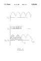
- FIG. 1 shows a schematic representation of a circuit applicable to the power supply
- FIG. 2 shows an actual circuit diagram applicable to the power supply
- FIG. 3 shows a series of waveforms applicable
- FIG. 4 shows voltage waveforms as measured at the points indicated by legends V 2 , V 3 and V 4 in FIGS. 1 and 2;
- FIG. 5 shows a modified form of the circuit diagram which illustrated in FIG. 2;
- FIG. 6 shows voltage waveforms as measured at the points indicated by legends V 2 and V 3 in FIG. 5.
- the power supply comprises a full-wave bridge rectifier 10, a low frequency current limiting inductor 11, a reservoir capacitor 12, a high frequency inductor 13, a solid state switching device 14 and an oscillator 15 which is employed to provide gating signals to the switching device 14.
- the voltage that appears across the switching device 14 is applied to a fluorescent tube 16, and a high pass capacitor 17 is located in series with the tube 16.
- a starter 18 in the form of a bimetal switch is connected between the filaments of the tube 16 in the usual way.
- the voltage supply for the oscillator 15 is derived as a proportion of the voltage V 2 across the reservoir capacitor, the gating signal from the oscillator 15 is effectively independent of voltage across the reservoir capacitor 12.
- the energising voltage V 4 which is applied to the tube 16 is obtained as a function of the voltage across the reservoir capacitor 12 and the frequency of the gaming signal from the oscillator 15.
- the capacitance value of the reservoir capacitor 12 is chosen to provide a high ripple voltage, that is to effect a relatively low level of smoothing, and at the same time to provide an instantaneous minimum level of ripple voltage which is sufficiently high to sustain operation of the oscillator 15 and maintain excitation of the tube 16. This latter aspect is described in more detail in the context of the circuit of FIG. 2 and the waveforms shown in FIG. 4 of the drawings. However, before proceeding with that description, brief reference is first made to the waveforms that are shown in FIG. 3.
- Waveform A represents the supply voltage V 1 which is applied to the ac side of the bridge rectifier 10.
- Waveform B represents the voltage that would appear at the dc side of the rectifier if the current from the rectifier were to flow into a purely resistive load, and waveform C represents the current that would flow into the ac side of the rectifier with such a resistive load connected in circuit with the rectifier.
- Waveform D represents the ripple voltage that would normally appear at the dc side of the rectifier of a prior art power supply circuit of a type that incorporates a reservoir capacitor having a typically "high" value of capacitance
- waveform E represents the current pulses that flow into the ac side of a rectifier of a power supply which produces a ripple voltage of the type shown in waveform D.
- Waveform F represents the ripple voltage that appears at the dc side of the rectifier 10 of the power supply of the present invention, that is a power supply having a reservoir capacitor 12 with a relatively "low" value of capacitance
- waveform G represents typically the current that flows into the ac side of the rectifier 10 as a consequence of the inclusion of a low value capacitance 12.
- FIG. 2 The power supply circuit which is shown schematically in FIG. 1 is illustrated in more detail in FIG. 2 and corresponding circuit elements are indicated by the same numerals in both figures. Further circuit components shown in FIG. 2 include a voltage dropping resistor 20 and a constant voltage power supply which comprises a diode 21, Zener diode 22 and low pass capacitor 23.
- the oscillator 15 shown in FIG. 2 comprises a 555 integrated circuit to which the constant voltage supply is connected via pins 4,8. Voltage divider resisters 24 and 25, diode 26 and capacitors 27 and 28 are provided to control the operation of the oscillator, including the period of oscillation and the mark-space ratio. With a 40 kHz output signal from the oscillator the circuit components may be chosen to provide an oscillator 0N period of up to 5 ⁇ S in a total period of 25 ⁇ S.
- the output signal V 3 from pin 3 of the oscillator 15 is applied to a switching device 14 in the form of a field effect transistor (FET).
- FET 14 is connected in circuit with the tube 16 in such manner that, when the FET is gated into conduction the instantaneous drain voltage V 4 applied to the tube 16 is zero and when the FET is gated OFF the instantaneous drain voltage applied to the tube rises to that which exists instantaneously at the drain side of the inductor 13.
- the value of the reservoir capacitor 12 may be selected to provide a minimum ripple voltage level in the order of 40 volts.
- the peak and minimum ripple voltage levels are indicated as such in FIG. 3F and these voltage levels increase to approximately 450 volts and 55 volts respectively at the FET drain when the FET is gated OFF, due to the influence of the inductor 13.
- the voltage applied to the tube 16 has a peak amplitude which varies over successive cycles with the voltage waveform across the reservoir capacitor 12. This is indicated schematically in FIG. 4 and in which, for ease of illustration, the period of each cycle of the gate voltage V 3 and the tube voltage V 4 is expanded relative to the period of the voltage V 2 across the reservoir capacitor.
- a reverse biased diode 29 and a metal oxide varistor (MOV) 30 are connected across the drain and source of the FET in order to protect the FET from any transient spikes that may appear in the power supply.
- MOV metal oxide varistor
- Circuit component types and values may be selected for specific applications but the following listing of circuit components is provided in respect of the power supply which is illustrated in FIG. 2 and which has been developed for use as a so-called electronic ballast for a 15 watt compact fluorescent lamp.
- FIG. 5 of the drawings illustrates a power supply which also meets the operating principles of the schematic circuit shown in FIG. 1 and like reference numerals are employed in FIG. 5 to identify components that are the same as those illustrated in FIGS. 1 and 2.
- the oscillator 15 is controlled to provide an ON time which increases with decreasing amplitude of the ripple voltage across the reservoir capacitor 12.
- FIG. 6 shows the output V 3 of the oscillator 15 plotted (on an expanded scale) with reference to the ripple voltage V 2 .
- a further 555 oscillator 31 is controlled by circuit components 32 to 34 to generate trigger pulses at pin 3 at a 40 kHz rate.
- the trigger pulses from oscillator 31 are applied to pin 2 of the oscillator 15, and oscillator 15 is in this case controlled by the divider network comprising resistors 36 to 38 and the RC network comprising components 39 and 40 to provide an ON time that increases from 2 ⁇ S to 8 ⁇ S with decreasing amplitude of the ripple voltage across the bridge rectifier 10.
- the capacitor 40 will charge rapidly to provide a short ON time of the oscillator 15, and low instantaneous values of ripple voltage will result in relatively longer capacitance charging times and proportionately longer ON times of the oscillator 15.
- Circuit component values that are applicable to the components in FIG. 5 are listed as follows.
- FIG. 5 As in the case of the circuit shown in FIG. 2, that which is illustrated in FIG. 5 has been developed as an electronic ballast for use with a 15 watt compact fluorescent lamp. Variations and modifications may be made in the circuit as above described in order to accommodate other applications of the circuit.
Abstract
Description
Claims (9)
Applications Claiming Priority (3)
| Application Number | Priority Date | Filing Date | Title |
|---|---|---|---|
| AUPL6811 | 1993-01-14 | ||
| AUPL681193 | 1993-01-14 | ||
| PCT/AU1993/000315 WO1994016492A1 (en) | 1993-01-14 | 1993-06-28 | Power supply |
Publications (1)
| Publication Number | Publication Date |
|---|---|
| US5528484A true US5528484A (en) | 1996-06-18 |
Family
ID=3776654
Family Applications (1)
| Application Number | Title | Priority Date | Filing Date |
|---|---|---|---|
| US08/302,822 Expired - Fee Related US5528484A (en) | 1993-01-14 | 1993-06-28 | Power supply |
Country Status (7)
| Country | Link |
|---|---|
| US (1) | US5528484A (en) |
| EP (1) | EP0636284B1 (en) |
| AT (1) | ATE170345T1 (en) |
| CA (1) | CA2132002A1 (en) |
| DE (1) | DE69320627D1 (en) |
| IL (1) | IL108268A (en) |
| WO (1) | WO1994016492A1 (en) |
Cited By (23)
| Publication number | Priority date | Publication date | Assignee | Title |
|---|---|---|---|---|
| US5936599A (en) * | 1995-01-27 | 1999-08-10 | Reymond; Welles | AC powered light emitting diode array circuits for use in traffic signal displays |
| US6137241A (en) * | 1996-08-08 | 2000-10-24 | Matsushita Electric Industrial Co., Ltd. | Starting switch circuit for a fluorescent lamp |
| US20060007679A1 (en) * | 1998-08-28 | 2006-01-12 | David Allen | LED assemblies and light strings containing same |
| US20070070622A1 (en) * | 2005-09-23 | 2007-03-29 | David Allen | Junction circuit for LED lighting chain |
| US20070164683A1 (en) * | 2006-01-17 | 2007-07-19 | David Allen | Unique lighting string rectification |
| US7276858B2 (en) | 2005-10-28 | 2007-10-02 | Fiber Optic Designs, Inc. | Decorative lighting string with stacked rectification |
| US20080024071A1 (en) * | 2006-07-31 | 2008-01-31 | Jingjing Yu | Bypass components in series wired led light strings |
| US20080025024A1 (en) * | 2006-07-31 | 2008-01-31 | Jingjing Yu | Parallel-series led light string |
| US20080084167A1 (en) * | 2004-10-01 | 2008-04-10 | Koninklijke Philips Electronics, N.V. | Power Converter for Led Large Area Light Source Lamp |
| US20080258649A1 (en) * | 2005-02-14 | 2008-10-23 | Jing Jing Yu | Interchangeable led bulbs |
| US20090027903A1 (en) * | 2004-11-10 | 2009-01-29 | Jing Jing Yu | Removable led lamp holder |
| US20090027899A1 (en) * | 2004-11-10 | 2009-01-29 | Jing Jing Yu | Removable led lamp holder with socket |
| US20090146167A1 (en) * | 1999-02-12 | 2009-06-11 | David Allen | Jacketed led assemblies removable from lamp husks and light strings containing same |
| US20090251923A1 (en) * | 2008-04-08 | 2009-10-08 | Jing Jing Yu | Water-resistant and replaceable led lamps |
| US7661852B2 (en) | 2005-07-26 | 2010-02-16 | 1 Energy Solutions, Inc. | Integrated LED bulb |
| US20100073963A1 (en) * | 2008-04-08 | 2010-03-25 | Jing Jing Yu | Water Resistant and Replaceable LED Lamps for Light Strings |
| WO2010038093A2 (en) * | 2008-09-30 | 2010-04-08 | Cathay Licensing Ltd | Electronic circuit and method for reducing the total harmonic distortion caused by dimming fluorescent lamps |
| US20100109560A1 (en) * | 2008-11-04 | 2010-05-06 | Jing Jing Yu | Capacitive Full-Wave Circuit for LED Light Strings |
| US7784993B2 (en) | 2007-07-13 | 2010-08-31 | 1 Energy Solutions, Inc. | Watertight LED lamp |
| US20100264806A1 (en) * | 2009-04-20 | 2010-10-21 | Beijing Yu | Led light bulbs in pyramidal structure for efficient heat dissipation |
| US20110051471A1 (en) * | 2009-08-26 | 2011-03-03 | Long Chen | Compact inverter plug for led light strings |
| US8083393B2 (en) | 2006-02-09 | 2011-12-27 | 1 Energy Solutions, Inc. | Substantially inseparable LED lamp assembly |
| US20170271982A1 (en) * | 2016-03-16 | 2017-09-21 | Curtis J. Dicke | Wide-voltage-range, direct rectification, power supply with inductive boost |
Families Citing this family (2)
| Publication number | Priority date | Publication date | Assignee | Title |
|---|---|---|---|---|
| US5804926A (en) * | 1996-04-08 | 1998-09-08 | Raytheon Company | Lighting circuit that includes a comparison of a "flattened" sinewave to a full wave rectified sinewave for control |
| AT13441U1 (en) * | 2011-12-23 | 2013-12-15 | Tridonic Gmbh & Co Kg | OPERATOR WITH POWER FACTOR CORRECTION |
Citations (8)
| Publication number | Priority date | Publication date | Assignee | Title |
|---|---|---|---|---|
| AU4285172A (en) * | 1971-06-28 | 1973-12-06 | Borgwarner Corporation | Improved single phase rectifier |
| GB2022943A (en) * | 1978-06-12 | 1979-12-19 | Siemens Ag | A.C. to D.C. converter |
| JPS5846868A (en) * | 1982-08-20 | 1983-03-18 | Toshiba Electric Equip Corp | Power supply |
| GB2133940A (en) * | 1983-01-14 | 1984-08-01 | Matsushita Electric Works Ltd | AC-DC-AC converter |
| US4564897A (en) * | 1983-01-13 | 1986-01-14 | Matsushita Electric Works, Ltd. | Power source |
| US4745539A (en) * | 1987-02-02 | 1988-05-17 | Nilssen Ole K | Controllable frequency converter |
| US4945467A (en) * | 1988-02-26 | 1990-07-31 | Black & Decker Inc. | Multiple-mode voltage converter |
| US5082998A (en) * | 1990-01-16 | 1992-01-21 | Yutaka Electric Mfg. Co., Ltd. | Switching power supply for microwave oven |
Family Cites Families (2)
| Publication number | Priority date | Publication date | Assignee | Title |
|---|---|---|---|---|
| US4348615A (en) * | 1980-07-01 | 1982-09-07 | Gte Products Corporation | Discharge lamp operating circuit |
| AU2163492A (en) * | 1991-06-19 | 1993-01-12 | Golden Power Electronics Pty Ltd | Electrical power supply |
-
1993
- 1993-06-28 WO PCT/AU1993/000315 patent/WO1994016492A1/en not_active Application Discontinuation
- 1993-06-28 AT AT93912465T patent/ATE170345T1/en not_active IP Right Cessation
- 1993-06-28 DE DE69320627T patent/DE69320627D1/en not_active Expired - Lifetime
- 1993-06-28 US US08/302,822 patent/US5528484A/en not_active Expired - Fee Related
- 1993-06-28 EP EP93912465A patent/EP0636284B1/en not_active Revoked
- 1993-06-28 CA CA002132002A patent/CA2132002A1/en not_active Abandoned
-
1994
- 1994-01-05 IL IL108268A patent/IL108268A/en not_active IP Right Cessation
Patent Citations (8)
| Publication number | Priority date | Publication date | Assignee | Title |
|---|---|---|---|---|
| AU4285172A (en) * | 1971-06-28 | 1973-12-06 | Borgwarner Corporation | Improved single phase rectifier |
| GB2022943A (en) * | 1978-06-12 | 1979-12-19 | Siemens Ag | A.C. to D.C. converter |
| JPS5846868A (en) * | 1982-08-20 | 1983-03-18 | Toshiba Electric Equip Corp | Power supply |
| US4564897A (en) * | 1983-01-13 | 1986-01-14 | Matsushita Electric Works, Ltd. | Power source |
| GB2133940A (en) * | 1983-01-14 | 1984-08-01 | Matsushita Electric Works Ltd | AC-DC-AC converter |
| US4745539A (en) * | 1987-02-02 | 1988-05-17 | Nilssen Ole K | Controllable frequency converter |
| US4945467A (en) * | 1988-02-26 | 1990-07-31 | Black & Decker Inc. | Multiple-mode voltage converter |
| US5082998A (en) * | 1990-01-16 | 1992-01-21 | Yutaka Electric Mfg. Co., Ltd. | Switching power supply for microwave oven |
Cited By (48)
| Publication number | Priority date | Publication date | Assignee | Title |
|---|---|---|---|---|
| US5936599A (en) * | 1995-01-27 | 1999-08-10 | Reymond; Welles | AC powered light emitting diode array circuits for use in traffic signal displays |
| US6137241A (en) * | 1996-08-08 | 2000-10-24 | Matsushita Electric Industrial Co., Ltd. | Starting switch circuit for a fluorescent lamp |
| US7344275B2 (en) | 1998-08-28 | 2008-03-18 | Fiber Optic Designs, Inc. | LED assemblies and light strings containing same |
| US20060007679A1 (en) * | 1998-08-28 | 2006-01-12 | David Allen | LED assemblies and light strings containing same |
| US9410668B2 (en) | 1999-02-12 | 2016-08-09 | Fiber Optic Designs, Inc. | Light strings including jacketed LED assemblies |
| US20060203482A1 (en) * | 1999-02-12 | 2006-09-14 | Allen Mark R | Jacketed LED assemblies and light strings containing same |
| US7220022B2 (en) | 1999-02-12 | 2007-05-22 | Fiber Optic Designs, Inc. | Jacketed LED assemblies and light strings containing same |
| US7931390B2 (en) | 1999-02-12 | 2011-04-26 | Fiber Optic Designs, Inc. | Jacketed LED assemblies and light strings containing same |
| US8840279B2 (en) | 1999-02-12 | 2014-09-23 | Fiber Optic Designs, Inc. | Jacketed LED assemblies and light strings containing same |
| US20090146167A1 (en) * | 1999-02-12 | 2009-06-11 | David Allen | Jacketed led assemblies removable from lamp husks and light strings containing same |
| US20060139920A1 (en) * | 2001-03-29 | 2006-06-29 | David Allen | Jacketed LED assemblies and light strings containing same |
| US7554822B2 (en) | 2004-10-01 | 2009-06-30 | Koninklijke Philips Electronics N.V. | Power converter for led large area light source lamp |
| US20080084167A1 (en) * | 2004-10-01 | 2008-04-10 | Koninklijke Philips Electronics, N.V. | Power Converter for Led Large Area Light Source Lamp |
| US7850361B2 (en) | 2004-11-10 | 2010-12-14 | 1 Energy Solutions, Inc. | Removable LED lamp holder |
| US20090027903A1 (en) * | 2004-11-10 | 2009-01-29 | Jing Jing Yu | Removable led lamp holder |
| US20090027899A1 (en) * | 2004-11-10 | 2009-01-29 | Jing Jing Yu | Removable led lamp holder with socket |
| US7850362B2 (en) | 2004-11-10 | 2010-12-14 | 1 Energy Solutions, Inc. | Removable LED lamp holder with socket |
| US20080258649A1 (en) * | 2005-02-14 | 2008-10-23 | Jing Jing Yu | Interchangeable led bulbs |
| US8823270B2 (en) | 2005-02-14 | 2014-09-02 | 1 Energy Solutions, Inc. | Interchangeable LED bulbs |
| US8016440B2 (en) | 2005-02-14 | 2011-09-13 | 1 Energy Solutions, Inc. | Interchangeable LED bulbs |
| US7661852B2 (en) | 2005-07-26 | 2010-02-16 | 1 Energy Solutions, Inc. | Integrated LED bulb |
| US20070070622A1 (en) * | 2005-09-23 | 2007-03-29 | David Allen | Junction circuit for LED lighting chain |
| US7265496B2 (en) | 2005-09-23 | 2007-09-04 | Fiber Optic Designs, Inc. | Junction circuit for LED lighting chain |
| US7276858B2 (en) | 2005-10-28 | 2007-10-02 | Fiber Optic Designs, Inc. | Decorative lighting string with stacked rectification |
| US20070164683A1 (en) * | 2006-01-17 | 2007-07-19 | David Allen | Unique lighting string rectification |
| US7250730B1 (en) | 2006-01-17 | 2007-07-31 | Fiber Optic Designs, Inc. | Unique lighting string rectification |
| US8083393B2 (en) | 2006-02-09 | 2011-12-27 | 1 Energy Solutions, Inc. | Substantially inseparable LED lamp assembly |
| US8388213B2 (en) | 2006-02-09 | 2013-03-05 | 1 Energy Solutions, Inc. | Substantially inseparable LED lamp assembly |
| US20080025024A1 (en) * | 2006-07-31 | 2008-01-31 | Jingjing Yu | Parallel-series led light string |
| US7963670B2 (en) | 2006-07-31 | 2011-06-21 | 1 Energy Solutions, Inc. | Bypass components in series wired LED light strings |
| US20080024071A1 (en) * | 2006-07-31 | 2008-01-31 | Jingjing Yu | Bypass components in series wired led light strings |
| US7784993B2 (en) | 2007-07-13 | 2010-08-31 | 1 Energy Solutions, Inc. | Watertight LED lamp |
| US20090251923A1 (en) * | 2008-04-08 | 2009-10-08 | Jing Jing Yu | Water-resistant and replaceable led lamps |
| US7883261B2 (en) | 2008-04-08 | 2011-02-08 | 1 Energy Solutions, Inc. | Water-resistant and replaceable LED lamps |
| US8376606B2 (en) | 2008-04-08 | 2013-02-19 | 1 Energy Solutions, Inc. | Water resistant and replaceable LED lamps for light strings |
| US20100073963A1 (en) * | 2008-04-08 | 2010-03-25 | Jing Jing Yu | Water Resistant and Replaceable LED Lamps for Light Strings |
| WO2010038093A3 (en) * | 2008-09-30 | 2010-09-30 | Cathay Licensing Ltd | Electronic circuit and method for reducing the total harmonic distortion caused by dimming fluorescent lamps |
| WO2010038093A2 (en) * | 2008-09-30 | 2010-04-08 | Cathay Licensing Ltd | Electronic circuit and method for reducing the total harmonic distortion caused by dimming fluorescent lamps |
| US20100109560A1 (en) * | 2008-11-04 | 2010-05-06 | Jing Jing Yu | Capacitive Full-Wave Circuit for LED Light Strings |
| US8314564B2 (en) | 2008-11-04 | 2012-11-20 | 1 Energy Solutions, Inc. | Capacitive full-wave circuit for LED light strings |
| US8723432B2 (en) | 2008-11-04 | 2014-05-13 | 1 Energy Solutions, Inc. | Capacitive full-wave circuit for LED light strings |
| US9955538B2 (en) | 2008-11-04 | 2018-04-24 | 1 Energy Solutions, Inc. | Capacitive full-wave circuit for LED light strings |
| US8297787B2 (en) | 2009-04-20 | 2012-10-30 | 1 Energy Solutions, Inc. | LED light bulbs in pyramidal structure for efficient heat dissipation |
| US20100264806A1 (en) * | 2009-04-20 | 2010-10-21 | Beijing Yu | Led light bulbs in pyramidal structure for efficient heat dissipation |
| US8836224B2 (en) | 2009-08-26 | 2014-09-16 | 1 Energy Solutions, Inc. | Compact converter plug for LED light strings |
| US20110051471A1 (en) * | 2009-08-26 | 2011-03-03 | Long Chen | Compact inverter plug for led light strings |
| US9226351B2 (en) | 2009-08-26 | 2015-12-29 | 1 Energy Solutions, Inc. | Compact converter plug for LED light strings |
| US20170271982A1 (en) * | 2016-03-16 | 2017-09-21 | Curtis J. Dicke | Wide-voltage-range, direct rectification, power supply with inductive boost |
Also Published As
| Publication number | Publication date |
|---|---|
| EP0636284B1 (en) | 1998-08-26 |
| ATE170345T1 (en) | 1998-09-15 |
| EP0636284A4 (en) | 1995-02-08 |
| WO1994016492A1 (en) | 1994-07-21 |
| DE69320627D1 (en) | 1998-10-01 |
| CA2132002A1 (en) | 1994-07-21 |
| EP0636284A1 (en) | 1995-02-01 |
| IL108268A (en) | 1998-03-10 |
| IL108268A0 (en) | 1994-04-12 |
Similar Documents
| Publication | Publication Date | Title |
|---|---|---|
| US5528484A (en) | Power supply | |
| US5396155A (en) | Self-dimming electronic ballast | |
| US6603274B2 (en) | Dimming ballast for compact fluorescent lamps | |
| JPH10506219A (en) | Externally dimmable electronic ballast | |
| JP3026681B2 (en) | Fluorescent light control device | |
| JPS648366B2 (en) | ||
| EP0622888B1 (en) | Improved power factor DC power supply | |
| KR19980032713A (en) | 2 wire power electronic switch | |
| US5440475A (en) | Electronic Ballast with low harmonic distortion | |
| US7157863B2 (en) | Device and method for the multi-phase operation of a gas discharge or metal vapor lamp | |
| JPS60207295A (en) | Ac operating circuit for high pressure gas discharge lamp | |
| JPH034492A (en) | Stabilizing circuit for discharge lamp | |
| JPH06507777A (en) | Power supply with high output coefficient along with control function to follow AC supply input | |
| AU672796B2 (en) | Power supply | |
| JP3319839B2 (en) | Discharge lamp lighting device | |
| US7521876B2 (en) | Electronic ballast with lamp type determination | |
| JP3323521B2 (en) | Discharge lamp lighting device | |
| JPS62207174A (en) | High frequency generator | |
| JP2532604B2 (en) | Induction heating device | |
| JP3050256B2 (en) | Discharge lamp lighting device | |
| JP2810677B2 (en) | Discharge lamp lighting device | |
| JP2802529B2 (en) | Discharge lamp lighting device | |
| JPH10302987A (en) | Lighting device for discharge lamp | |
| JPH05219724A (en) | Power supply and discharge lamp lighting device | |
| JPH07213068A (en) | Inverter |
Legal Events
| Date | Code | Title | Description |
|---|---|---|---|
| AS | Assignment |
Owner name: H.P.M. INDUSTRIES PTY LIMITED, AUSTRALIA Free format text: ASSIGNMENT OF ASSIGNORS INTEREST;ASSIGNOR:HAYASHI, KOICHI;REEL/FRAME:007258/0308 Effective date: 19940906 |
|
| FEPP | Fee payment procedure |
Free format text: PAYOR NUMBER ASSIGNED (ORIGINAL EVENT CODE: ASPN); ENTITY STATUS OF PATENT OWNER: LARGE ENTITY |
|
| FPAY | Fee payment |
Year of fee payment: 4 |
|
| FPAY | Fee payment |
Year of fee payment: 8 |
|
| REMI | Maintenance fee reminder mailed | ||
| LAPS | Lapse for failure to pay maintenance fees | ||
| STCH | Information on status: patent discontinuation |
Free format text: PATENT EXPIRED DUE TO NONPAYMENT OF MAINTENANCE FEES UNDER 37 CFR 1.362 |
|
| FP | Lapsed due to failure to pay maintenance fee |
Effective date: 20080618 |