US5548553A - Method and apparatus for providing high-speed column redundancy - Google Patents
Method and apparatus for providing high-speed column redundancy Download PDFInfo
- Publication number
- US5548553A US5548553A US08/353,603 US35360394A US5548553A US 5548553 A US5548553 A US 5548553A US 35360394 A US35360394 A US 35360394A US 5548553 A US5548553 A US 5548553A
- Authority
- US
- United States
- Prior art keywords
- columns
- column
- input
- bus
- output
- Prior art date
- Legal status (The legal status is an assumption and is not a legal conclusion. Google has not performed a legal analysis and makes no representation as to the accuracy of the status listed.)
- Expired - Lifetime
Links
Images


Classifications
-
- G—PHYSICS
- G11—INFORMATION STORAGE
- G11C—STATIC STORES
- G11C29/00—Checking stores for correct operation ; Subsequent repair; Testing stores during standby or offline operation
- G11C29/70—Masking faults in memories by using spares or by reconfiguring
- G11C29/78—Masking faults in memories by using spares or by reconfiguring using programmable devices
- G11C29/80—Masking faults in memories by using spares or by reconfiguring using programmable devices with improved layout
- G11C29/802—Masking faults in memories by using spares or by reconfiguring using programmable devices with improved layout by encoding redundancy signals
-
- G—PHYSICS
- G11—INFORMATION STORAGE
- G11C—STATIC STORES
- G11C29/00—Checking stores for correct operation ; Subsequent repair; Testing stores during standby or offline operation
- G11C29/70—Masking faults in memories by using spares or by reconfiguring
- G11C29/78—Masking faults in memories by using spares or by reconfiguring using programmable devices
- G11C29/84—Masking faults in memories by using spares or by reconfiguring using programmable devices with improved access time or stability
- G11C29/848—Masking faults in memories by using spares or by reconfiguring using programmable devices with improved access time or stability by adjacent switching
Definitions
- This invention relates in general to semiconductor memory devices, and more particularly to semiconductor memory devices including redundant cells for replacing faults within the memory device.
- a memory device to include defects that will prevent the device from operating properly. These possible defects include short circuits between adjacent columns or rows or open circuits within individual columns or rows of the memory device, as well as non-functional clusters of cells.
- defects may be easily identified by a testing procedure after fabrication.
- a semiconductor memory device with a defect is inoperable, and would have to be discarded.
- the semiconductor memory devices have been designed to include a redundancy circuit having a number of redundant cells to replace the defective memory cells.
- redundancy In memory devices which provide row redundancy, the memory device is apportioned into a discrete number of blocks. For each block, an extra set of rows are provided. If, during testing, it is discovered that a row or two adjacent rows or a cluster of cells within the pitch of a pair of rows in a block is defective, the redundant set for the block is substituted for the defective cells. To activate the redundant circuitry, appropriate fuses are included for programming individual decoder circuits to be responsive to the addresses of the defective set of rows.
- the first drawback is that it is ineffective against bit-line failures, that is when an entire column of the semiconductor memory device fails.
- the second drawback is that although at least a pair of rows is often provided as the redundant set for the block, that set may be ineffective to provide sufficient replacement capability for large clustered defects.
- a second type of redundancy is to provide redundant columns in the semiconductor memory device.
- usually at least a pair of redundant columns is allocated to a predetermined number of columns.
- a memory array having a 64 bit data path may provide a redundant column pair for each byte of information, thereby providing 8 redundant column pairs.
- column redundancy provides a technique for replacing bit-line failures, the available methods of providing column redundancy are complex and therefore do not make optimal use of the available semiconductor area.
- An additional problem associated with redundant column design is the increased propagation delay through the semi-conductor device caused by the additional redundant logic. Thus, for memory devices in which the redundant column logic is utilized, because the timing of the device is adversely impacted the device may have to be sold at a discount even though it is utilizing more expensive hardware.
- a method for correcting errors in a memory device includes the steps of providing at least one redundant column in a memory array having a plurality of columns, the plurality of columns coupled to a bus having a corresponding plurality of bit locations, each of the columns having an input path and an output path, the input and output paths coupled to the corresponding bit location of the bus.
- the method further includes the step of bypassing one of said plurality of columns in the event that the one of said columns is defective, where the step of bypassing the one of the columns comprising the defect includes the step of coupling the bit locations of the bus corresponding to the columns between the defective column and the redundant column, including the bit location of said bus corresponding to the defective column, to the input and output path of the column adjacent to said corresponding column in the direction of the redundant column.
- an apparatus for correcting memory defects includes at least one redundant column of data and means, responsive to one of the columns of the memory being defective, for rearranging the correspondence between the bits on the bus and the columns of memory such that the redundant column stores data for one of the columns of the plurality of columns and another of said columns of the plurality of columns stores data for the defective column.
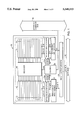
- FIG. 1 is a block diagram of a semiconductor memory device including a redundant store according to the invention
- FIG. 2 is an exploded block diagram for use in illustrating the substitution of the redundant store in the semiconductor device of FIG. 1;
- FIG. 3 is a flow diagram illustrating a method for controlling the substitution of the redundant store of FIG. 2.
- an illustrative 4K ⁇ 8 bit semiconductor memory device 10 is shown to include a memory array 11 (shown by dashed lines in FIG. 1) which is physically divided into two 2K ⁇ 8 sub-arrays 12 and 14.
- Each of the 2K sub-arrays 12 and 14 comprise 66 rows of 33 columns of 8-bit data.
- each of the 2K sub-arrays 12 and 14 includes redundant column store 13 and 15, respectively, for use in repairing bit-line failures as will be further described herein.
- Each redundant column store 13 and 15 comprises 66 rows by 1 8-bit column of redundant storage logic.
- Sub-arrays 12 and 14, and redundant column stores 13 and 15 are coupled to receive index data from a word-line decoder 16.
- Word-line decoder 16 receives address data from control logic 25 via lines 25a.
- Control logic 25 is coupled to address/command bus 40.
- sub-arrays 12 and 14 provide 33 columns of 8 bit data to multiplexers 18 and 20, respectively.
- redundant stores 13 and 15 each provide 1 column of 8 bit data to bit-slice multiplexers 18 and 20, respectively.
- the select inputs of multiplexers 18 and 20 are coupled to receive a decode of column address bits from control logic 25, to select one of the eight bits, or the desired ⁇ bit slice ⁇ , for output on the data bus 42.
- Each of the bit-slice multiplexers 18 and 20 is coupled by a 34 bit bus to redundancy multiplexers 22 and 24, respectively.
- the 34 bit bus 18a and 20a thus carries the selected bit slice for each of the 33 data columns from sub-arrays 12 and 14 as well as the bit-slice from the redundant columns 13 and 15 to the redundancy multiplexers.
- the select inputs of multiplexers 22 and 24 are coupled to fuses 32 and 34.
- the multiplexers 22 and 24 are coupled to input/output driver 36.
- Input/output driver 36 includes a number of transceivers and sense amplifiers for receiving and transmitting data onto data bus 42.
- control logic 25 receives an address and a command via bus 40. In response, the control logic 25 provides row address information to word-line decoder 16 to drive a row of data in the sub-arrays 12 and 14 and the redundant stores 13 and 15.
- word-line decoder 16 When the word-line decoder selects the row of memory from sub-arrays 12 and 14 and redundant stores 13 and 15, 264 bits of data from each of the sub-arrays and 8 bits of data from each of the redundant data stores are input to each of the bit-slice multiplexers 18 and 20.
- the appropriate bit slice is selected, and 34 bits of data are propagated to each of the redundancy multiplexers 22 and 24.
- redundancy multiplexers 22 and 24 select 33 of the 34 bits provided from bit-slice multiplexers 18 and 20. As a result, sixty-six bits of data are driven by input/output buffers 36 onto data bus 42 for each memory access. The method for selecting which of the 34 bits are to be provided as output from each half of the memory array 11 is described in detail below.
- the redundancy multiplexers 22 and 24 operate in conjunction with the redundant stores 13 and 15, respectively, to repair defects in respective sub-arrays in the following manner.
- one half of memory device 10 is shown, incorporating outputs from the sub-array 14, outputs from the redundant storage 15, multiplexer logic 24, and fuses 34.
- the other half of the memory device, incorporating outputs of sub-array 12, multiplexer 18, fuses 32 and outputs of redundant store 13 operates substantially similar to the elements described in FIG. 2, and thus for ease of explanation will not be described in detail.
- the elements 14a-14d represent the selected bit slice for four columns of sub-array 14.
- Element 15a represents the selected bit slice from the redundant store 15. Although the selected bit slice for all of the 33 columns of the sub-array has not been shown, it is to be understood that the connections shown with regard to the selected bit-slice of columns 0-3 are representative of the arrangement of the selected bit-slices of subsequent columns in the sub-array.
- Multiplexer logic 24 is shown to include a pair of 2:1 multiplexers for each of the 33 columns of data in memory sub-array 14.
- Each multiplexer pair for example multiplexer pair 50 (shown outlined) for column 0 data, includes an output multiplexer 50a and an input multiplexer 50b.
- the input multiplexer 50b is coupled to input/output driver 36 (FIG. 1) for receiving column 0 data from bus 42 during a write operation of the memory device.
- Column 0 data is also used as an input for the selected bit-slice of redundant store 15.
- Input multiplexer 50b receives as its second input the bit data from the input/output drivers corresponding to the next physically adjacent column in memory.
- column 0 is shown to receive data from the column 1 input bit of the data bus 42. Assuming that the input multiplexer 50a was enabled to select the column 1 input bit for storage in the column 0 store 14a, in effect the data stored in memory sub-array 14 has been shifted to the right relative to the location of the data bit on data bus 42.
- the output multiplexer 50a is coupled to transmit data to the input/output driver 36, to provide data to the column 0 location of data bus 42.
- the output multiplexer 50a receives as inputs data from column 0 of sub-array 14, and data from redundant store 15. Data from each column is also provided to the output multiplexer of the next physically adjacent column of memory.
- data from column 0 of sub-array 14 is also provided as a potential source of column 1 output data.
- the column arrangement of FIG. 2 facilitates a right shift of data for reads and writes
- the objects of the invention are independent of the direction in which data is shifted between memory locations. If, for example, the redundant column was located adjacent to column 32, rather than column 0, (as shown with reference to sub-array 12 in FIG. 1) the direction of the shifts for read and write operations would be a left shift. It is the ability to perform the data shift, rather than the direction of the shift, which enables fast access of redundant store information for repairing defective memory locations, and example of which is described below.
- the select values of the multiplexer pair 50 are provided by an associated decoder, for example decoder 52.
- the decoder 52 receives an encoded shift amount from fuses 32.
- the encoded shift amount comprises 6 bits (to encompass values from 0 to 33) and represents the number of columns that must shift their data in order to bypass the redundant column. To bypass the defective column, the correspondence between the bit number on the bus and the column number in sub-array is rearranged, or shifted, by one in the direction of the redundant column.
- each decoder compares the encoded shift amount against its column address +1. For example, the decode logic of column 0, decoder 52, compares the received shift amount against the value ⁇ 1 ⁇ (column 0+1).
- the corresponding decoder If the encoded shift value is less than or equal to the column address +1, at step 64 the corresponding decoder provides a select value to enable the shifting of data between columns. Otherwise, at step 66, the corresponding decoder drives the select line of the multiplexer pair 50 so that data is sourced from the associated column.
- the encoded shift amount could also be provided in the form of a binary mask having a number of bits equal to the number of columns, and with each bit indicating whether or not the multiplexer should shift its inputs and outputs.
- the decision as to whether or not to encode the shift amount is a matter of design depending on the number of columns and the available area.
- the routing of a 33 bit mask through the memory device is less desirable than encoding the mask into 6 bits and later decoding to determine the select.
- other methods of storing a shift amount or a mask may be used in addition to the use of fuse 34. For example, internal control registers that get initiated at power up by built in self test logic could also be used.
- Bits M-(N+1) are stored in columns M-(N+1), respectively;
- Bits N-1 are stored in columns (N-1)-0, respectively.
- Bit 0 is stored in R, the redundant column.
- the bits are reallocated in the following manner:
- Bit M is stored in R
- Bits (M-1) ⁇ N are stored in columns M ⁇ N+1, respectively.
- Bits (N-1) ⁇ 0 are stored in columns (N-1) ⁇ 0; respectively.
- the total delay added to the propagation delay in adding redundant column is the minimal propagation delay of a 2:1 multiplexer, no matter which of the columns includes the defective bit.
- the same delay is seen by all of the bits of the memory device, thus ensuring that all of the bits of the memory are provided substantially simultaneously.
- fuse 34 (FIG. 1) stores an encoded shift amount for sub-array 14
- fuse 32 may store a different encoded shift amount for sub-array 12.
- two discrete bit-line failures per memory device may be corrected per semi-conductor memory device with only a minimal increase to the propagation delay of the semiconductor device.
- the above described configuration allows for a small number of redundant columns of memory to be added to a design while maintaining maximal coverage.
- the above described method may alleviate the problem of bit-line failures without the known propagation problems and complexities associated with previously developed column redundancy methods.
Abstract
Description
Claims (10)
Priority Applications (1)
| Application Number | Priority Date | Filing Date | Title |
|---|---|---|---|
| US08/353,603 US5548553A (en) | 1994-12-12 | 1994-12-12 | Method and apparatus for providing high-speed column redundancy |
Applications Claiming Priority (1)
| Application Number | Priority Date | Filing Date | Title |
|---|---|---|---|
| US08/353,603 US5548553A (en) | 1994-12-12 | 1994-12-12 | Method and apparatus for providing high-speed column redundancy |
Publications (1)
| Publication Number | Publication Date |
|---|---|
| US5548553A true US5548553A (en) | 1996-08-20 |
Family
ID=23389822
Family Applications (1)
| Application Number | Title | Priority Date | Filing Date |
|---|---|---|---|
| US08/353,603 Expired - Lifetime US5548553A (en) | 1994-12-12 | 1994-12-12 | Method and apparatus for providing high-speed column redundancy |
Country Status (1)
| Country | Link |
|---|---|
| US (1) | US5548553A (en) |
Cited By (32)
| Publication number | Priority date | Publication date | Assignee | Title |
|---|---|---|---|---|
| US5742556A (en) * | 1996-12-26 | 1998-04-21 | Micro Magic, Inc. | Redundancy scheme for semiconductor RAMS |
| US5793683A (en) * | 1997-01-17 | 1998-08-11 | International Business Machines Corporation | Wordline and bitline redundancy with no performance penalty |
| US5812466A (en) * | 1995-10-04 | 1998-09-22 | Samsung Electronics Co., Ltd. | Column redundancy circuit for a semiconductor memory device |
| US5841710A (en) * | 1997-02-14 | 1998-11-24 | Micron Electronics, Inc. | Dynamic address remapping decoder |
| US5923599A (en) * | 1996-04-29 | 1999-07-13 | Texas Instruments Incorporated | Apparatus and method for subarray testing in dynamic random access memories using a built-in-self-test unit |
| US5936900A (en) * | 1996-12-19 | 1999-08-10 | Texas Instruments Incorporated | Integrated circuit memory device having built-in self test circuit with monitor and tester modes |
| US6021512A (en) * | 1996-11-27 | 2000-02-01 | International Business Machines Corporation | Data processing system having memory sub-array redundancy and method therefor |
| US6115300A (en) * | 1998-11-03 | 2000-09-05 | Silicon Access Technology, Inc. | Column redundancy based on column slices |
| US6128240A (en) * | 1997-08-22 | 2000-10-03 | Micron Technology, Inc. | Cancellation of redundant elements with a cancel bank |
| US6243301B1 (en) * | 1998-11-27 | 2001-06-05 | Matsushita Electric Industrial Co., Ltd. | Semiconductor memory device and signal line switching circuit |
| US6278403B1 (en) | 1999-09-17 | 2001-08-21 | Sirf Technology, Inc. | Autonomous hardwired tracking loop coprocessor for GPS and WAAS receiver |
| US6314527B1 (en) | 1998-03-05 | 2001-11-06 | Micron Technology, Inc. | Recovery of useful areas of partially defective synchronous memory components |
| US6332183B1 (en) | 1998-03-05 | 2001-12-18 | Micron Technology, Inc. | Method for recovery of useful areas of partially defective synchronous memory components |
| US6337818B1 (en) * | 2000-06-20 | 2002-01-08 | Mitsubishi Denki Kabushiki Kaisha | Semiconductor memory device having a redundancy construction |
| US6381707B1 (en) | 1998-04-28 | 2002-04-30 | Micron Technology, Inc. | System for decoding addresses for a defective memory array |
| US6381708B1 (en) | 1998-04-28 | 2002-04-30 | Micron Technology, Inc. | Method for decoding addresses for a defective memory array |
| US6496876B1 (en) | 1998-12-21 | 2002-12-17 | Micron Technology, Inc. | System and method for storing a tag to identify a functional storage location in a memory device |
| US6526322B1 (en) | 1999-12-16 | 2003-02-25 | Sirf Technology, Inc. | Shared memory architecture in GPS signal processing |
| US20030072197A1 (en) * | 2001-09-14 | 2003-04-17 | Jeon Byung Deuk | Semiconductor memory device which can recover a memory fail |
| US6578157B1 (en) | 2000-03-06 | 2003-06-10 | Micron Technology, Inc. | Method and apparatus for recovery of useful areas of partially defective direct rambus rimm components |
| US20030206477A1 (en) * | 1997-11-12 | 2003-11-06 | Waller William K. | Device and method for repairing a semiconductor memory |
| US6671620B1 (en) | 2000-05-18 | 2003-12-30 | Sirf Technology, Inc. | Method and apparatus for determining global position using almanac information |
| US20040010737A1 (en) * | 1996-04-25 | 2004-01-15 | Merritt Todd A. | Layout for a semiconductor memory device having redundant elements |
| US20040022110A1 (en) * | 2002-07-30 | 2004-02-05 | Mitsubishi Denki Kabushiki Kaisha | Semiconductor memory device storing redundant replacement information with small occupation area |
| US6735727B1 (en) * | 1999-06-03 | 2004-05-11 | Samsung Electronics Co., Ltd. | Flash memory device with a novel redundancy selection circuit and method of using the same |
| US20050022084A1 (en) * | 1996-04-30 | 2005-01-27 | Hii Kuong Hua | Built-in self-test arrangement for integrated circuit memory devices |
| US7134057B1 (en) * | 2004-02-13 | 2006-11-07 | Sun Microsystems, Inc. | Off-pitch column redundancy using dynamic shifters |
| US20070030742A1 (en) * | 2005-08-02 | 2007-02-08 | Micron Technology, Inc. | Combination column redundancy system for a memory array |
| US7269765B1 (en) | 2000-04-13 | 2007-09-11 | Micron Technology, Inc. | Method and apparatus for storing failing part locations in a module |
| US8116976B2 (en) | 2000-05-18 | 2012-02-14 | Csr Technology Inc. | Satellite based positioning method and system for coarse location positioning |
| US20150302939A1 (en) * | 2014-04-22 | 2015-10-22 | George P. Hoekstra | Memory with redundancy |
| US10592367B2 (en) * | 2017-09-15 | 2020-03-17 | Apple Inc. | Redundancy implementation using bytewise shifting |
Citations (2)
| Publication number | Priority date | Publication date | Assignee | Title |
|---|---|---|---|---|
| US4598388A (en) * | 1985-01-22 | 1986-07-01 | Texas Instruments Incorporated | Semiconductor memory with redundant column circuitry |
| US4603404A (en) * | 1981-12-29 | 1986-07-29 | Fujitsu Limited | Semiconductor memory device with redundant cells |
-
1994
- 1994-12-12 US US08/353,603 patent/US5548553A/en not_active Expired - Lifetime
Patent Citations (2)
| Publication number | Priority date | Publication date | Assignee | Title |
|---|---|---|---|---|
| US4603404A (en) * | 1981-12-29 | 1986-07-29 | Fujitsu Limited | Semiconductor memory device with redundant cells |
| US4598388A (en) * | 1985-01-22 | 1986-07-01 | Texas Instruments Incorporated | Semiconductor memory with redundant column circuitry |
Cited By (50)
| Publication number | Priority date | Publication date | Assignee | Title |
|---|---|---|---|---|
| US5812466A (en) * | 1995-10-04 | 1998-09-22 | Samsung Electronics Co., Ltd. | Column redundancy circuit for a semiconductor memory device |
| US7043672B2 (en) * | 1996-04-25 | 2006-05-09 | Micron Technology, Inc. | Layout for a semiconductor memory device having redundant elements |
| US20040010737A1 (en) * | 1996-04-25 | 2004-01-15 | Merritt Todd A. | Layout for a semiconductor memory device having redundant elements |
| US5923599A (en) * | 1996-04-29 | 1999-07-13 | Texas Instruments Incorporated | Apparatus and method for subarray testing in dynamic random access memories using a built-in-self-test unit |
| US20050022084A1 (en) * | 1996-04-30 | 2005-01-27 | Hii Kuong Hua | Built-in self-test arrangement for integrated circuit memory devices |
| US7278078B2 (en) | 1996-04-30 | 2007-10-02 | Texas Instruments Incorporated | Built-in self-test arrangement for integrated circuit memory devices |
| US6021512A (en) * | 1996-11-27 | 2000-02-01 | International Business Machines Corporation | Data processing system having memory sub-array redundancy and method therefor |
| US5936900A (en) * | 1996-12-19 | 1999-08-10 | Texas Instruments Incorporated | Integrated circuit memory device having built-in self test circuit with monitor and tester modes |
| US5742556A (en) * | 1996-12-26 | 1998-04-21 | Micro Magic, Inc. | Redundancy scheme for semiconductor RAMS |
| US5793683A (en) * | 1997-01-17 | 1998-08-11 | International Business Machines Corporation | Wordline and bitline redundancy with no performance penalty |
| US5841710A (en) * | 1997-02-14 | 1998-11-24 | Micron Electronics, Inc. | Dynamic address remapping decoder |
| US6128240A (en) * | 1997-08-22 | 2000-10-03 | Micron Technology, Inc. | Cancellation of redundant elements with a cancel bank |
| US6633507B2 (en) | 1997-08-22 | 2003-10-14 | Micron Technology, Inc. | Cancellation of redundant elements with a cancel bank |
| US6690611B2 (en) | 1997-08-22 | 2004-02-10 | Micron Technology, Inc | Cancellation of redundant elements with a cancel bank |
| US6351424B1 (en) | 1997-08-22 | 2002-02-26 | Micron Technology, Inc. | Cancellation of redundant elements with a cancel bank |
| US6693833B2 (en) * | 1997-11-12 | 2004-02-17 | Micron Technology, Inc. | Device and method for repairing a semiconductor memory |
| US20030206477A1 (en) * | 1997-11-12 | 2003-11-06 | Waller William K. | Device and method for repairing a semiconductor memory |
| US6332183B1 (en) | 1998-03-05 | 2001-12-18 | Micron Technology, Inc. | Method for recovery of useful areas of partially defective synchronous memory components |
| US6314527B1 (en) | 1998-03-05 | 2001-11-06 | Micron Technology, Inc. | Recovery of useful areas of partially defective synchronous memory components |
| US6621748B2 (en) | 1998-03-05 | 2003-09-16 | Micron Technology, Inc. | Recovery of useful areas of partially defective synchronous memory components |
| US6381708B1 (en) | 1998-04-28 | 2002-04-30 | Micron Technology, Inc. | Method for decoding addresses for a defective memory array |
| US6381707B1 (en) | 1998-04-28 | 2002-04-30 | Micron Technology, Inc. | System for decoding addresses for a defective memory array |
| US6115300A (en) * | 1998-11-03 | 2000-09-05 | Silicon Access Technology, Inc. | Column redundancy based on column slices |
| US6243301B1 (en) * | 1998-11-27 | 2001-06-05 | Matsushita Electric Industrial Co., Ltd. | Semiconductor memory device and signal line switching circuit |
| US6496876B1 (en) | 1998-12-21 | 2002-12-17 | Micron Technology, Inc. | System and method for storing a tag to identify a functional storage location in a memory device |
| US6735727B1 (en) * | 1999-06-03 | 2004-05-11 | Samsung Electronics Co., Ltd. | Flash memory device with a novel redundancy selection circuit and method of using the same |
| US6480150B2 (en) | 1999-09-17 | 2002-11-12 | Sirf Technology, Inc. | Autonomous hardwired tracking loop coprocessor for GPS and WAAS receiver |
| US6278403B1 (en) | 1999-09-17 | 2001-08-21 | Sirf Technology, Inc. | Autonomous hardwired tracking loop coprocessor for GPS and WAAS receiver |
| US6930634B2 (en) | 1999-12-16 | 2005-08-16 | Sirf Technology, Inc. | Shared memory architecture in GPS signal processing |
| US6526322B1 (en) | 1999-12-16 | 2003-02-25 | Sirf Technology, Inc. | Shared memory architecture in GPS signal processing |
| US6578157B1 (en) | 2000-03-06 | 2003-06-10 | Micron Technology, Inc. | Method and apparatus for recovery of useful areas of partially defective direct rambus rimm components |
| US6810492B2 (en) | 2000-03-06 | 2004-10-26 | Micron Technology, Inc. | Apparatus and system for recovery of useful areas of partially defective direct rambus RIMM components |
| US20070288805A1 (en) * | 2000-04-13 | 2007-12-13 | Charlton David E | Method and apparatus for storing failing part locations in a module |
| US7269765B1 (en) | 2000-04-13 | 2007-09-11 | Micron Technology, Inc. | Method and apparatus for storing failing part locations in a module |
| US7890819B2 (en) | 2000-04-13 | 2011-02-15 | Micron Technology, Inc. | Method and apparatus for storing failing part locations in a module |
| US8116976B2 (en) | 2000-05-18 | 2012-02-14 | Csr Technology Inc. | Satellite based positioning method and system for coarse location positioning |
| US6671620B1 (en) | 2000-05-18 | 2003-12-30 | Sirf Technology, Inc. | Method and apparatus for determining global position using almanac information |
| US8260548B2 (en) | 2000-05-18 | 2012-09-04 | Csr Technology Inc. | Satellite based positioning method and system for coarse location positioning |
| US6337818B1 (en) * | 2000-06-20 | 2002-01-08 | Mitsubishi Denki Kabushiki Kaisha | Semiconductor memory device having a redundancy construction |
| US20030072197A1 (en) * | 2001-09-14 | 2003-04-17 | Jeon Byung Deuk | Semiconductor memory device which can recover a memory fail |
| US6930933B2 (en) * | 2001-09-14 | 2005-08-16 | Hynix Semiconductor Inc. | Semiconductor memory device which can recover a memory fail |
| US20040022110A1 (en) * | 2002-07-30 | 2004-02-05 | Mitsubishi Denki Kabushiki Kaisha | Semiconductor memory device storing redundant replacement information with small occupation area |
| US7254069B2 (en) * | 2002-07-30 | 2007-08-07 | Renesas Technology Corp. | Semiconductor memory device storing redundant replacement information with small occupation area |
| US7433251B2 (en) | 2002-07-30 | 2008-10-07 | Renesas Technology Corp. | Semiconductor memory device storing redundant replacement information with small occupation area |
| US7134057B1 (en) * | 2004-02-13 | 2006-11-07 | Sun Microsystems, Inc. | Off-pitch column redundancy using dynamic shifters |
| US7251173B2 (en) | 2005-08-02 | 2007-07-31 | Micron Technology, Inc. | Combination column redundancy system for a memory array |
| US20070030742A1 (en) * | 2005-08-02 | 2007-02-08 | Micron Technology, Inc. | Combination column redundancy system for a memory array |
| US20150302939A1 (en) * | 2014-04-22 | 2015-10-22 | George P. Hoekstra | Memory with redundancy |
| US9672938B2 (en) * | 2014-04-22 | 2017-06-06 | Nxp Usa, Inc. | Memory with redundancy |
| US10592367B2 (en) * | 2017-09-15 | 2020-03-17 | Apple Inc. | Redundancy implementation using bytewise shifting |
Similar Documents
| Publication | Publication Date | Title |
|---|---|---|
| US5548553A (en) | Method and apparatus for providing high-speed column redundancy | |
| JP3822412B2 (en) | Semiconductor memory device | |
| US5796662A (en) | Integrated circuit chip with a wide I/O memory array and redundant data lines | |
| US5313425A (en) | Semiconductor memory device having an improved error correction capability | |
| JP3588246B2 (en) | Processor-based embedded self-test macro and integrated circuit chip | |
| KR100200985B1 (en) | Redundant circuit apparatus | |
| JP2590897B2 (en) | Semiconductor memory | |
| JP4111762B2 (en) | Semiconductor memory device | |
| JPH0574191A (en) | Semiconductor memory device | |
| KR100325035B1 (en) | Semiconductor memory device | |
| JPH08147995A (en) | Semiconductor memory device | |
| KR20090030762A (en) | Semiconductor memory device having redundancy memory block and cell array structure of the same | |
| JPH07254270A (en) | Method and apparatus for control of plurality of banks of dram element | |
| JP3799197B2 (en) | Semiconductor memory device | |
| US6914833B2 (en) | Apparatus for random access memory array self-repair | |
| US6373775B2 (en) | Semiconductor memory device with restrained scale of decoding circuit used in shift redundancy | |
| US6366508B1 (en) | Integrated circuit memory having column redundancy with no timing penalty | |
| JP3814464B2 (en) | Semiconductor memory integrated circuit | |
| KR940006079B1 (en) | Semiconductor memory device | |
| JP3751810B2 (en) | Semiconductor memory device | |
| US7055075B2 (en) | Apparatus for random access memory array self-test | |
| JPH04368700A (en) | Semiconductor memory device | |
| US7073102B2 (en) | Reconfiguration device for faulty memory | |
| JPH0652697A (en) | Semiconductor memory having error correcting function | |
| US6754865B2 (en) | Integrated circuit |
Legal Events
| Date | Code | Title | Description |
|---|---|---|---|
| AS | Assignment |
Owner name: DIGITAL EQUIPMENT CORPORATION, MASSACHUSETTS Free format text: ASSIGNMENT OF ASSIGNORS INTEREST;ASSIGNORS:COOPER, ELIZABETH MORROW;LEARY, MICHAEL;REEL/FRAME:007282/0302;SIGNING DATES FROM 19941123 TO 19941205 |
|
| STCF | Information on status: patent grant |
Free format text: PATENTED CASE |
|
| FPAY | Fee payment |
Year of fee payment: 4 |
|
| AS | Assignment |
Owner name: COMPAQ INFORMATION TECHNOLOGIES GROUP, L.P., TEXAS Free format text: ASSIGNMENT OF ASSIGNORS INTEREST;ASSIGNORS:DIGITAL EQUIPMENT CORPORATION;COMPAQ COMPUTER CORPORATION;REEL/FRAME:012447/0903;SIGNING DATES FROM 19991209 TO 20010620 |
|
| AS | Assignment |
Owner name: HEWLETT-PACKARD DEVELOPMENT COMPANY, L.P., TEXAS Free format text: CHANGE OF NAME;ASSIGNOR:COMPAQ INFORMANTION TECHNOLOGIES GROUP LP;REEL/FRAME:014102/0224 Effective date: 20021001 |
|
| FPAY | Fee payment |
Year of fee payment: 8 |
|
| FPAY | Fee payment |
Year of fee payment: 12 |
|
| REMI | Maintenance fee reminder mailed |