US5548734A - Equal length symmetric computer bus topology - Google Patents
Equal length symmetric computer bus topology Download PDFInfo
- Publication number
- US5548734A US5548734A US08/368,716 US36871695A US5548734A US 5548734 A US5548734 A US 5548734A US 36871695 A US36871695 A US 36871695A US 5548734 A US5548734 A US 5548734A
- Authority
- US
- United States
- Prior art keywords
- bus
- computer
- printed circuit
- circuit board
- connectors
- Prior art date
- Legal status (The legal status is an assumption and is not a legal conclusion. Google has not performed a legal analysis and makes no representation as to the accuracy of the status listed.)
- Expired - Lifetime
Links
Images


Classifications
-
- H—ELECTRICITY
- H05—ELECTRIC TECHNIQUES NOT OTHERWISE PROVIDED FOR
- H05K—PRINTED CIRCUITS; CASINGS OR CONSTRUCTIONAL DETAILS OF ELECTRIC APPARATUS; MANUFACTURE OF ASSEMBLAGES OF ELECTRICAL COMPONENTS
- H05K1/00—Printed circuits
- H05K1/02—Details
- H05K1/0213—Electrical arrangements not otherwise provided for
- H05K1/0237—High frequency adaptations
- H05K1/0248—Skew reduction or using delay lines
-
- G—PHYSICS
- G06—COMPUTING; CALCULATING OR COUNTING
- G06F—ELECTRIC DIGITAL DATA PROCESSING
- G06F13/00—Interconnection of, or transfer of information or other signals between, memories, input/output devices or central processing units
- G06F13/38—Information transfer, e.g. on bus
- G06F13/40—Bus structure
- G06F13/4063—Device-to-bus coupling
- G06F13/409—Mechanical coupling
-
- H—ELECTRICITY
- H05—ELECTRIC TECHNIQUES NOT OTHERWISE PROVIDED FOR
- H05K—PRINTED CIRCUITS; CASINGS OR CONSTRUCTIONAL DETAILS OF ELECTRIC APPARATUS; MANUFACTURE OF ASSEMBLAGES OF ELECTRICAL COMPONENTS
- H05K1/00—Printed circuits
- H05K1/02—Details
- H05K1/0213—Electrical arrangements not otherwise provided for
- H05K1/0216—Reduction of cross-talk, noise or electromagnetic interference
- H05K1/0228—Compensation of cross-talk by a mutually correlated lay-out of printed circuit traces, e.g. for compensation of cross-talk in mounted connectors
-
- H—ELECTRICITY
- H05—ELECTRIC TECHNIQUES NOT OTHERWISE PROVIDED FOR
- H05K—PRINTED CIRCUITS; CASINGS OR CONSTRUCTIONAL DETAILS OF ELECTRIC APPARATUS; MANUFACTURE OF ASSEMBLAGES OF ELECTRICAL COMPONENTS
- H05K1/00—Printed circuits
- H05K1/02—Details
- H05K1/14—Structural association of two or more printed circuits
-
- H—ELECTRICITY
- H05—ELECTRIC TECHNIQUES NOT OTHERWISE PROVIDED FOR
- H05K—PRINTED CIRCUITS; CASINGS OR CONSTRUCTIONAL DETAILS OF ELECTRIC APPARATUS; MANUFACTURE OF ASSEMBLAGES OF ELECTRICAL COMPONENTS
- H05K2201/00—Indexing scheme relating to printed circuits covered by H05K1/00
- H05K2201/04—Assemblies of printed circuits
- H05K2201/044—Details of backplane or midplane for mounting orthogonal PCBs
-
- H—ELECTRICITY
- H05—ELECTRIC TECHNIQUES NOT OTHERWISE PROVIDED FOR
- H05K—PRINTED CIRCUITS; CASINGS OR CONSTRUCTIONAL DETAILS OF ELECTRIC APPARATUS; MANUFACTURE OF ASSEMBLAGES OF ELECTRICAL COMPONENTS
- H05K2201/00—Indexing scheme relating to printed circuits covered by H05K1/00
- H05K2201/09—Shape and layout
- H05K2201/09009—Substrate related
- H05K2201/09027—Non-rectangular flat PCB, e.g. circular
-
- H—ELECTRICITY
- H05—ELECTRIC TECHNIQUES NOT OTHERWISE PROVIDED FOR
- H05K—PRINTED CIRCUITS; CASINGS OR CONSTRUCTIONAL DETAILS OF ELECTRIC APPARATUS; MANUFACTURE OF ASSEMBLAGES OF ELECTRICAL COMPONENTS
- H05K2201/00—Indexing scheme relating to printed circuits covered by H05K1/00
- H05K2201/09—Shape and layout
- H05K2201/09209—Shape and layout details of conductors
- H05K2201/09218—Conductive traces
- H05K2201/09236—Parallel layout
-
- H—ELECTRICITY
- H05—ELECTRIC TECHNIQUES NOT OTHERWISE PROVIDED FOR
- H05K—PRINTED CIRCUITS; CASINGS OR CONSTRUCTIONAL DETAILS OF ELECTRIC APPARATUS; MANUFACTURE OF ASSEMBLAGES OF ELECTRICAL COMPONENTS
- H05K2201/00—Indexing scheme relating to printed circuits covered by H05K1/00
- H05K2201/09—Shape and layout
- H05K2201/09209—Shape and layout details of conductors
- H05K2201/09218—Conductive traces
- H05K2201/09254—Branched layout
-
- H—ELECTRICITY
- H05—ELECTRIC TECHNIQUES NOT OTHERWISE PROVIDED FOR
- H05K—PRINTED CIRCUITS; CASINGS OR CONSTRUCTIONAL DETAILS OF ELECTRIC APPARATUS; MANUFACTURE OF ASSEMBLAGES OF ELECTRICAL COMPONENTS
- H05K2201/00—Indexing scheme relating to printed circuits covered by H05K1/00
- H05K2201/09—Shape and layout
- H05K2201/09209—Shape and layout details of conductors
- H05K2201/09218—Conductive traces
- H05K2201/09263—Meander
Definitions
- This invention relates to digital computer bus systems. More specifically to an equal length symmetric bus topology that reduces the impact of transmission line reflections.
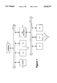
- FIG. 1 illustrates in block diagram form, a typical computer system with a bus 15.
- the bus 15 connects the processor 11 to memory 13 and to various Input/Output (“I/O") devices 12, such as displays, keyboards, etc.
- I/O Input/Output
- FIG. 1 illustrates a computer system with a main computer bus 15 and a secondary computer bus 17.
- the computer system uses the main computer bus 15 for high-speed memory access and other time critical functions.
- the secondary bus 17 operates at a slower speed in order to accommodate slower I/O devices 19.
- a bus controller 18 couples the main computer bus 15 to the secondary computer bus 17.
- a typical microcomputer bus is physically constructed of a set of parallel traces embedded in a printed circuit board. Most microcomputers incorporate the computer bus as electrical traces etched on the main printed circuit board called the motherboard.
- each of the bus signals in the bus 15 begin to exhibit transmission line effects which can degrade the quality of the bus signal.
- One type of transmission line effect that degrades signal quality is a transmission line reflection. Impedance discontinuities along the signal path of a bus signal cause transmission line reflections to occur. At each point in a signal path where an impedance change occurs, a transmission line reflection will be generated. The greater the impedance mismatch, the greater the transmission line reflection will be.
- each bus signal path extends from a central junction point to each node on the computer bus.
- the signal paths are of equal length and have identical electrical characteristics.
- FIG. 1 is a block diagram of a computer bus used to communicate information between different parts of a computer system.
- FIG. 2a is an electrical diagram of a transmission line.
- FIG. 2b is a lattice diagram of the transmission line reflections that occur when a voltage source sends a step voltage down the transmission line illustrated in FIG. 2a.
- FIG. 2c is a plot of the voltage levels at the driver end and the receiver end of a transmission line when a voltage source sends a step voltage down the transmission line illustrated in FIG. 2a.
- FIG. 3a illustrates an ideal digital signal
- FIG. 3b illustrates an analog electrical signal used to represent the ideal digital signal given in FIG. 3a.
- FIG. 3c illustrates how the analog electrical signal of FIG. 3a appears in digital form.
- FIG. 4a is a block diagram of a typical prior art computer bus.
- FIG. 4b is a transmission line model of the prior art computer bus in FIG. 4a.
- FIG. 4c is a plot of the voltage levels at a driver node and a receiver node when the driver node sends a step voltage to the receiver node on a prior art computer bus.
- FIG. 5a is a block diagram of a computer bus with an equal length symmetric topology.
- FIG. 5b is a transmission line model of the computer bus with an equal length symmetric topology.
- FIG. 5c is a plot of the voltage levels at a driver node and a receiver node when the driver node sends a step voltage to the receiver node on the computer bus with an equal length symmetric topology.
- FIG. 6 is a diagram of a possible embodiment of a computer bus with an equal length symmetric topology.
- FIG. 7a is a diagram of a typical prior art computer bus.
- FIG. 7b is a diagram of a possible embodiment of a computer bus with an equal length symmetric topology.
- FIG. 8 is a diagram of the present invention being used to implement tracings to the outermost connectors in an IBM® Micro Channel® bus with six connectors.
- FIG. 9 is a diagram of the present invention being used to implement tracings to the middle connectors in an IBM® Micro Channel® bus with six connectors.
- FIG. 10 is a diagram of the present invention being used to implement tracings to the innermost connectors in an IBM® Micro Channel® bus with six connectors.
- FIG. 2a illustrates a transmission line with a line impedance of Z 0 and a delay per unit length of T pd .
- a voltage source V i At one end of the transmission line is a voltage source V i and a source impedance of Z s .
- a load At the other end of the transmission line is a load with an impedance of Z t .
- the source impedance Z s , the transmission line impedance of Z 0 , and the load impedance of Z t are not perfectly matched, the impedance mismatch will generate transmission line reflections on the transmission line.
- the transmission line impedance is Z 0
- the load voltage reflection coefficient r t at the point V t is defined the equation: ##EQU1##
- the source voltage reflection coefficient r s at the point Vs is defined by the equation: ##EQU2##
- the load voltage reflection coefficient r t and the source voltage reflection coefficient r s define the amount of voltage that the impedance mismatches at the load impedance and the source impedance reflect back, respectively.
- the voltage source V i drives the transmission line with a step voltage
- a series of reflections will occur back and forth across the transmission line until a steady state voltage level is reached.
- the voltage source V i drives the transmission line with a unit step voltage (1 V)
- a voltage division first occurs dividing voltage V i between source impedance Z s and transmission line impedance Z 0 . This creates an initial voltage at point V s that can be calculated using the equation: ##EQU3##
- This voltage travels down the transmission line until it reaches the load impedance Z t . At that point the load reflects back some voltage as determined by the load voltage reflection coefficient r t defined above.
- the voltage source reflects half of the reflected voltage back again towards the load as determined by the source voltage reflection coefficient r s as defined above.
- FIG. 2b provides a lattice diagram of the voltage reflections that occur in the system.
- the voltage reflections continue back and forth across the transmission line until the transmission line reaches a steady state voltage level.
- the steady state voltage level (V ss ) at both of the points V s and V t is calculated by dividing the steady state input voltage V i between source impedance Z s and load impedance Z t : ##EQU4##
- FIG. 2c illustrates a plot of the voltage levels at the voltage source end of the transmission line V s and at the load end of the transmission line V t when a voltage source sends unit step voltage down the transmission line. It is apparent from the voltage plot of FIG. 2c that the transmission line reflections caused by impedance mismatch make the electrical signal oscillate above and below the steady state voltage level V ss .
- FIG. 3a illustrates an ideal digital signal.
- the ideal digital signal always is either at a logic high level (“1") or a logic low level (“0"). At the points where the ideal digital signal switches logic levels, the change takes place instantaneously.
- FIG. 3b illustrates an analog electrical signal at the input of digital device used to represent the ideal digital signal given in FIG. 3a.
- two input voltage levels V IH and V IL are marked. These levels represent the high level input and the low level input threshold voltages respectively.
- V IH high level input threshold voltage
- V IL low level input threshold voltage
- the electrical signal at the output of a digital device indicates a logic high level.
- the electrical signal at the output of a digital device indicates a logic low level.
- the electrical signal voltage is between the high level input threshold voltage V IH and the low level input threshold voltage V IL , the signal is invalid and should not be sampled. This situation occurs when the device is switching.
- the transitions between logic high input and logic low input levels cannot take place instantaneously.
- the electrical signal changes from a logic low state to a logic high state during time period C the electrical signal is neither high nor low.
- This time period is referred to as the signal rise time.
- the electrical signal changes from a logic high state to a logic low state during time period G there is another time period where the electrical signal is neither high nor low. This time period is referred to as the signal fall time.
- the analog electrical signal is invalid and should not be sampled.
- FIG. 3c illustrates how a digital device interprets the analog electrical signal of FIG. 3b appears when the analog electrical signal is connected to a digital device.
- a logic high value is presented.
- a logic low value is presented.
- Time periods K-O of FIG. 3b illustrate an oscillation caused by a transmission line reflection.
- the signal is above the high level input threshold value.
- a transmission line reflection temporarily forces the signal is below the high level input threshold value V IH .
- the dip below the high level input threshold value V IH is referred to as an undershoot.
- time period M in FIG. 3c when the electrical signal drops below the high level input threshold value V IH , the output of the digital device may transition to the logic level low for a short period of time causing voltage glitch.
- the glitch is illustrated as a logic low in FIG. 3c for time period M.
- the electrical signal in FIG. 3b again rises above the high level input threshold value V IH causing the digital interpretation in FIG. 3c to be a logic high level.
- the undershoot in time period M at the input of a digital device may cause a logic level low glitch.
- This glitch can cause a false triggering of the device which receives the signal.
- the undershoot in time period M causes problems for synchronous buses.
- a computer system propagates both a clock signal and data signals on the bus.
- a receiver uses the rising edge of the clock signal to latch in the data.
- the clock signal must monotonically pass through the threshold region between V IL and V IH to correctly clock in the data.
- the signal changes from a logic low level to a logic high level twice in a row, as illustrated in time periods K-L and M-O, the signal will likely accidentally trigger the receiver to latch in invalid data. This occurs since the first rising edge latches in the correct data and the second rising edge caused by the undershoot latches in data when the data is no longer valid at the input of the device.
- FIG. 4a illustrates, in block diagram form, a prior art microcomputer bus.
- the microcomputer bus of FIG. 4a consists of a backplane bus 15, several nodes 10, and stubs 17 connecting each node 10 to the backplane bus 15.
- the bus illustrated in FIG. 4a has n parallel lines for carrying n different signals.
- Each node 10 on the bus can act as a driver or a receiver of signals.
- the nodes 10 share the bus according to a defined bus protocol.
- the backplane bus 15 of a microcomputer is usually constructed of a printed circuit board with a set of n embedded electrical traces.
- the stubs 17 are electrical sockets electrically connected to the printed circuit board traces.
- the individual nodes 10 are usually printed circuit board cards which can be inserted into the electrical sockets to expand the computer system as needed.
- FIG. 4b illustrates an electrical diagram of the computer bus of FIG. 4a in which the signal path along the backplane has been modeled as a transmission line.
- node 1 has been designated as a signal driver.
- the driver, node 1 is modeled as a voltage source 41 and a source impedance Z s .
- the remaining nodes 2-7 have been modeled as receiver nodes.
- the receiver nodes 2-7 have been assigned impedance loads Z 2 -Z 7 .
- the backplane bus acts as a transmission line.
- the stubs are very small, the stubs will not have any significant effect on the transmission line model.
- the stubs are therefore modeled as direct connections that do not effect the transmission line model.
- the signal When the voltage source 41 of the driver node 1 drives a signal, the signal propagates along the backplane bus to each of the other nodes 2-7. As the signal reaches each receiver node, the impedance mismatch between the backplane transmission line and the receiver impedance produces a voltage reflection that propagates back down the bus backplane to the voltage source 41. For example, when the driver node 1 drives a signal, the signal would first travel through the stub of the first node and along the backplane until it reaches the stub for node 2. At this point, the impedance mismatch between the backplane transmission line and the load impedance Z 2 produces a first voltage reflection. The signal continues along the backplane transmission line until it reaches the stub for node 3. At the stub for node 3, the impedance mismatch between the backplane transmission line and the load impedance Z 3 generates a second voltage reflection. The signal continues along the backplane transmission line producing a voltage reflection at each node.
- the transmission line reflections distort the waveforms produced at the driver node and the receiver nodes.
- the distortion produced at the driver node is not a problem since no device samples the waveform at the driver.
- the distortions at the receiver nodes are a problem.
- the distortion produced by the transmission line reflections is most apparent at the receiver nodes nearest the driver node. In FIG. 4b for example, the transmission line reflections produced from the impedance mismatch at nodes 3-7 distort the waveform at node 2, the node nearest the driver node.
- FIG. 4c illustrates a plot of the voltage levels at the driver node 1 and at the receiver node 2 for the prior art computer bus depicted in FIG. 4a and FIG. 4b when the driver at node 1 drives a signal from a logic low state to a logic high state and back to a logic low state again.
- the driver voltage increases linearly.
- transmission line reflections begin to distort the waveform of the driver signal.
- the receiver signal initially increases linearly until transmission line reflections begin to distort the receiver waveform.
- the receiver signal rises above the high level input threshold value V IH , but then a transmission line reflection temporarily forces the signal below the high level input threshold value V IH .
- the undershoot at point 45 can accidentally cause devices connected to the receiver node to trigger twice.
- FIG. 5a provides an illustration of the bus topology of the present invention.
- the bus of the present invention has a number of nodes 10 that can both transmit and receive bus signals.
- the bus of the present invention is not implemented as a set of parallel lines with nodes branching off. Instead, each node 10 has a signal path 23 that leads to a central junction point 21.
- the signal paths 23 are constructed such that the signal path 23 from each node 10 to the central junction point 21 is of a predetermined equal length and each signal path 23 has the same electrical characteristics. All the receiver nodes 10 must have the same electrical characteristics.
- FIG. 5b illustrates a transmission line model of the equal length symmetric bus of the present invention illustrated in FIG. 5a.
- a driver node is modeled as a voltage source 51 and a source impedance Z s .
- Each of the receiver nodes 2-7 are modeled as load impedances Z 2 -Z 7 .
- Each signal path 23 leading from the central junction point 21 to a receiver load impedance is modeled as a transmission line.
- the signal When the voltage source 51 in the driver node drives a signal, the signal first passes through the source impedance and a first stretch of transmission line. The signal then reaches the central junction point 21 where there is a severe impedance mismatch. At the central junction point 21, the signal experiences a change from traveling on a path with an impedance of Z 0 to traveling on several parallel paths with a net path of impedance of: ##EQU5##
- FIG. 5c illustrates a plot of the voltage levels at the driver node and a receiver node for the symmetric equal length computer bus depicted in FIG. 5a and FIG. 5b when the driver at node 1 drives a signal from a logic low state to a logic high state and back to a logic low state again. Since all the receiver nodes are identical in the symmetric equal length computer bus, the waveforms at all the receiver nodes are identical. Initially, the driver voltage increases linearly. At point 52, a transmission line reflection from the central junction point 21 forces the waveform of the driver signal down. The receiver signal, however, increases linearly straight through the threshold region bounded by the high level input threshold value V IH and the low level input threshold value V IL . No undershoot is caused by the transmission line reflections.
- the equal length symmetric computer bus of the present invention is therefore superior to prior art computer buses.
- the equal length symmetric computer bus of the present invention also provides additional advantages. Since transmission path from the driver to every receiver is of equal length, there is an equal propagation delay from the driver to all the receivers. Furthermore, there is no signal skew between the receivers.
- each bus node In order to construct an equal length symmetric computer bus, the electrical lines from each bus node must be of equal length and the electrical properties of each electrical line must be identical.
- FIG. 6 illustrates an equal length symmetric computer bus constructed in this manner. At the center of FIG. 6 is a row of central nodes 65. Extending radially outward from each central node are six equal length electrical traces 68. At the end of each set of electrical traces 68 is a bus connector 61.
- the equal length symmetric computer bus illustrated in FIG. 6 has several disadvantages.
- the layout of the bus connectors 61 in the computer bus system of FIG. 6 is very nonstandard. Two pairs of bus connectors 61 are in line with one other thereby placing a limitation on the length of the circuit boards that can be inserted.
- the equal length lines 68 must cross over each other several times near the central nodes 65. Each time the traces cross over one another, the board requires more than one printed circuit board layer.
- the layout of the bus system causes the printed circuit board 62 to have a very non standard hexagonal form-factor that requires a large amount of space. It is desirable to instead implement an equal length symmetric computer bus that is compatible with the current motherboard layout in personal computers.
- most personal computers implement the computer bus as a set of parallel traces 68 parallel to one edge of the mother board 62.
- a number of bus connectors 61 are spaced along the parallel bus traces 68 perpendicular to the bus traces 68.
- FIG. 7b illustrates the traces required for a single symmetric equal length bus signal in a six node system.
- the row of central junction points 65 is centered between the six bus connectors 61.
- a first pair of traces 68 extends from the outermost bus connectors to the central junction point 65.
- the traces 68 from the outermost bus connectors are almost completely straight, bending only to route around the pins from the inner bus connectors.
- a second pair of traces 67 extends from the second outermost bus connectors to the central junction point 65.
- the second pair of traces 67 contains an extra bend that initially extends slightly away from the central junction point 65, and then routes back to the central junction point 65. The extra bend away from the central junction point creates extra length in the traces 67 to make the traces 67 the same length as the traces 68.
- a third pair of traces 66 extends from the innermost bus connectors to the central junction point 65.
- the traces 66 contain a larger extra bend that initially extends away from the central junction point 65 almost reaching the next bus connector, and then returns to the central junction point 65. The extra bend provides added length to the traces 66 to make the traces 66 the same length as the traces 67 and 68.
- the traces of different bus signals should be placed some minimum distance from one another. It has been determined that if the traces are of a thickness D, there should be a minimum distance of 3D between the bus signal traces and any other traces to prevent crosstalk. For example, if the bus signal traces are 6 thousandths of an inch wide, there should be a minimum distance of 18 thousandths of an inch between the bus signal traces and any other electrical traces. The traces should be routed closely together in parallel such that an equal length symmetric bus with any number of signals can be constructed.
- FIGS. 8, 9, and 10 illustrate an expandable symmetric equal length bus topology as taught by the present invention using the IBM® Micro Channel® bus connector.
- the outer two rows pins 81 and 82 are used to carry bus signals.
- the inner two rows pins 83 are used only as power and ground pins. Traces extend from each of the pins in the two rows of bus signal pins 81 and 82 to two central junction point rows 85 and 86 respectively. Although the traces for only 8 bus signals are illustrated, the traces are routed closely together in parallel such that any number of bus signals can be connected.
- the printed circuit board traces for the bus signals are placed onto three separate printed circuit board layers.
- a first printed circuit board layer illustrated in FIG. 8 connects the two outermost of bus connectors.
- a second printed circuit board layer illustrated in FIG. 9 connects the next inner pair of bus connectors.
- a third printed circuit board layer illustrated in FIG. 10 connects the two innermost of bus connectors.
- FIG. 8 illustrates the first printed circuit board layer containing the traces from the outermost bus connectors.
- the traces 68 run almost straight from the bus signal pins to the central junction rows 85 and 86. Slight bends are made in the traces to avoid the pins of the inner bus connectors.
- the second printed circuit board layer containing the traces from the next outer bus connectors is illustrated.
- the traces 67 have a slight bend 71 that initially extends away from the central junction rows 85 and 86 then travel back to the central junction rows 85 and 86.
- the slight bend 71 adds extra length to the traces 67 to make the traces 67 the same length as the traces 68 from the printed circuit board layer in FIG. 8.
- FIG. 10 illustrates the third printed circuit board layer containing the traces from the next outer bus connectors.
- the traces 66 have a slight bend 72 that initially extends away from the central junction rows 85 and 86 then travel back to the central junction rows 85 and 86.
- the slight bend 72 adds extra length to the traces 66 to make the traces 66 the same length as the traces 68 and the traces 67 from the printed circuit board layer in FIGS. 8 and 9 respectively.
Abstract
An equal length symmetric computer bus topology. The equal length symmetric computer bus topology provides a bus signal path to a number of bus nodes. Each bus signal path extends from each node on the computer bus to a central junction point. The bus signal paths are of equal length and have identical electrical characteristics. The equal length symmetric computer bus topology minimizes the effect of transmission line reflections upon the bus signals. The equal length symmetric computer bus topology also causes very little clock skew.
Description
This is a continuation of application Ser. No. 08/038,235, filed Mar. 26, 1993, now abandoned.
1. Field of the Invention
This invention relates to digital computer bus systems. More specifically to an equal length symmetric bus topology that reduces the impact of transmission line reflections.
2. Art Background
A digital computer employs a computer bus to communicate information between the different parts of the computer system. Buses are simply a set of parallel electrical lines used to communicate information signals. FIG. 1 illustrates in block diagram form, a typical computer system with a bus 15. The bus 15 connects the processor 11 to memory 13 and to various Input/Output ("I/O") devices 12, such as displays, keyboards, etc.
There can be more than one bus in a single computer system. FIG. 1 illustrates a computer system with a main computer bus 15 and a secondary computer bus 17. The computer system uses the main computer bus 15 for high-speed memory access and other time critical functions. The secondary bus 17 operates at a slower speed in order to accommodate slower I/O devices 19. A bus controller 18 couples the main computer bus 15 to the secondary computer bus 17.
A typical microcomputer bus is physically constructed of a set of parallel traces embedded in a printed circuit board. Most microcomputers incorporate the computer bus as electrical traces etched on the main printed circuit board called the motherboard.
The clock speeds of modern computer processors are continually increasing in order to achieve faster performance. This is especially true for microprocessor based computer systems. As a result, the buses that the processors use to communicate information between the different parts of a computer system also need to function at increasingly higher frequencies. Computer designers, therefore need to carefully design computer buses to handle the higher operating frequencies in order to maintain high quality bus signals.
When the operating frequency of a computer bus, such as the bus 15 illustrated in FIG. 1, becomes very high, each of the bus signals in the bus 15 begin to exhibit transmission line effects which can degrade the quality of the bus signal. One type of transmission line effect that degrades signal quality is a transmission line reflection. Impedance discontinuities along the signal path of a bus signal cause transmission line reflections to occur. At each point in a signal path where an impedance change occurs, a transmission line reflection will be generated. The greater the impedance mismatch, the greater the transmission line reflection will be.
There are often a number of impedance discontinuities along the signal path of a computer bus signal. Common computer bus signal impedance discontinuities include mismatched loads, electrical connectors, line stubs, device input, and board layer changes. It is therefore desirable to design a computer bus that minimizes the effect transmission line reflections have on the signals.
It is therefore an object of the present invention to provide a computer bus structure that minimizes the effect of transmission line reflections and provides high quality computer bus signals.
It is a further object of the present invention to provide a bus structure that transmits bus signals from a bus driver to several bus receivers with an equal propagation delay from the bus driver to all the bus receivers.
It is a further object of the present invention to provide a bus structure that transmits bus signals to several receivers with minimal signal skew between the receivers.
These and other objectives are accomplished by the equal length symmetric bus topology of the present invention. In the bus topology of the present invention each bus signal path extends from a central junction point to each node on the computer bus. The signal paths are of equal length and have identical electrical characteristics.
The objects, features and advantages of the present invention will be apparent to one skilled in the art, in view of the following detailed description in which:
FIG. 1 is a block diagram of a computer bus used to communicate information between different parts of a computer system.
FIG. 2a is an electrical diagram of a transmission line.
FIG. 2b is a lattice diagram of the transmission line reflections that occur when a voltage source sends a step voltage down the transmission line illustrated in FIG. 2a.
FIG. 2c is a plot of the voltage levels at the driver end and the receiver end of a transmission line when a voltage source sends a step voltage down the transmission line illustrated in FIG. 2a.
FIG. 3a illustrates an ideal digital signal.
FIG. 3b illustrates an analog electrical signal used to represent the ideal digital signal given in FIG. 3a.
FIG. 3c illustrates how the analog electrical signal of FIG. 3a appears in digital form.
FIG. 4a is a block diagram of a typical prior art computer bus.
FIG. 4b is a transmission line model of the prior art computer bus in FIG. 4a.
FIG. 4c is a plot of the voltage levels at a driver node and a receiver node when the driver node sends a step voltage to the receiver node on a prior art computer bus.
FIG. 5a is a block diagram of a computer bus with an equal length symmetric topology.
FIG. 5b is a transmission line model of the computer bus with an equal length symmetric topology.
FIG. 5c is a plot of the voltage levels at a driver node and a receiver node when the driver node sends a step voltage to the receiver node on the computer bus with an equal length symmetric topology.
FIG. 6 is a diagram of a possible embodiment of a computer bus with an equal length symmetric topology.
FIG. 7a is a diagram of a typical prior art computer bus.
FIG. 7b is a diagram of a possible embodiment of a computer bus with an equal length symmetric topology.
FIG. 8 is a diagram of the present invention being used to implement tracings to the outermost connectors in an IBM® Micro Channel® bus with six connectors.
FIG. 9 is a diagram of the present invention being used to implement tracings to the middle connectors in an IBM® Micro Channel® bus with six connectors.
FIG. 10 is a diagram of the present invention being used to implement tracings to the innermost connectors in an IBM® Micro Channel® bus with six connectors.
An equal length symmetric computer bus topology is disclosed. In the following description, for purposes of explanation, specific nomenclature is set forth to provide a thorough understanding of the present invention. However, it will be apparent to one skilled in the art that these specific details are not required in order to practice the present invention. In other instances, well known circuits and devices are shown in block diagram form in order not to obscure the present invention unnecessarily.
FIG. 2a illustrates a transmission line with a line impedance of Z0 and a delay per unit length of Tpd. At one end of the transmission line is a voltage source Vi and a source impedance of Zs. At the other end of the transmission line is a load with an impedance of Zt. When the source impedance Zs, the transmission line impedance of Z0, and the load impedance of Zt are not perfectly matched, the impedance mismatch will generate transmission line reflections on the transmission line.
For example, consider the case where the transmission line impedance is Z0, the source impedance is Zs =0.33Z0, and the load impedance is Zt =2Z0. The load voltage reflection coefficient rt at the point Vt is defined the equation: ##EQU1## Similarly, the source voltage reflection coefficient rs at the point Vs is defined by the equation: ##EQU2## The load voltage reflection coefficient rt and the source voltage reflection coefficient rs define the amount of voltage that the impedance mismatches at the load impedance and the source impedance reflect back, respectively.
If, for example, the voltage source Vi drives the transmission line with a step voltage, a series of reflections will occur back and forth across the transmission line until a steady state voltage level is reached. When the voltage source Vi drives the transmission line with a unit step voltage (1 V), a voltage division first occurs dividing voltage Vi between source impedance Zs and transmission line impedance Z0. This creates an initial voltage at point Vs that can be calculated using the equation: ##EQU3## This voltage travels down the transmission line until it reaches the load impedance Zt. At that point the load reflects back some voltage as determined by the load voltage reflection coefficient rt defined above. The total voltage at point Vt is equal to the incoming voltage plus the reflected voltage which is 0.75 V(1+rt)=0.75 V(1+0.33)=1 V. The reflected voltage (0.75 V*rt =0.25 V) travels back to the voltage source. When the reflected voltage reaches the voltage source, the voltage source reflects half of the reflected voltage back again towards the load as determined by the source voltage reflection coefficient rs as defined above. FIG. 2b provides a lattice diagram of the voltage reflections that occur in the system.
The voltage reflections continue back and forth across the transmission line until the transmission line reaches a steady state voltage level. The steady state voltage level (Vss) at both of the points Vs and Vt is calculated by dividing the steady state input voltage Vi between source impedance Zs and load impedance Zt : ##EQU4##
FIG. 2c illustrates a plot of the voltage levels at the voltage source end of the transmission line Vs and at the load end of the transmission line Vt when a voltage source sends unit step voltage down the transmission line. It is apparent from the voltage plot of FIG. 2c that the transmission line reflections caused by impedance mismatch make the electrical signal oscillate above and below the steady state voltage level Vss.
FIG. 3a illustrates an ideal digital signal. The ideal digital signal always is either at a logic high level ("1") or a logic low level ("0"). At the points where the ideal digital signal switches logic levels, the change takes place instantaneously.
FIG. 3b illustrates an analog electrical signal at the input of digital device used to represent the ideal digital signal given in FIG. 3a. On the vertical axis, two input voltage levels VIH and VIL are marked. These levels represent the high level input and the low level input threshold voltages respectively. When the electrical signal input voltage is above the high level input threshold voltage VIH, the electrical signal at the output of a digital device indicates a logic high level. When the electrical signal voltage is below the low level input threshold voltage VIL, the electrical signal at the output of a digital device indicates a logic low level. When the electrical signal voltage is between the high level input threshold voltage VIH and the low level input threshold voltage VIL, the signal is invalid and should not be sampled. This situation occurs when the device is switching.
Referring to the analog electrical signal of FIG. 3b, the transitions between logic high input and logic low input levels cannot take place instantaneously. For example, when the electrical signal changes from a logic low state to a logic high state during time period C the electrical signal is neither high nor low. This time period is referred to as the signal rise time. Similarly, when the electrical signal changes from a logic high state to a logic low state during time period G there is another time period where the electrical signal is neither high nor low. This time period is referred to as the signal fall time. During either the rise time or the fall time, the analog electrical signal is invalid and should not be sampled.
FIG. 3c illustrates how a digital device interprets the analog electrical signal of FIG. 3b appears when the analog electrical signal is connected to a digital device. During the periods where the electrical signal is above the high level input threshold voltage VIH, a logic high value is presented. During the periods where the electrical signal is below the low level input threshold voltage VIL, a logic low value is presented. When the electrical signal is between the high level input threshold voltage VIH and the low level input threshold voltage VIL such as rise time period C and fall time period G, the output of a digital device is in transition between the logic levels and the output is undefined.
As demonstrated in the previous section, transmission line reflections degrade the quality of electrical signals by causing voltage oscillations before transmission line reaches a steady state voltage level. Time periods K-O of FIG. 3b illustrate an oscillation caused by a transmission line reflection. At time period L, the signal is above the high level input threshold value. However, at time period M a transmission line reflection temporarily forces the signal is below the high level input threshold value VIH. The dip below the high level input threshold value VIH is referred to as an undershoot. Referring to time period M in FIG. 3c, when the electrical signal drops below the high level input threshold value VIH, the output of the digital device may transition to the logic level low for a short period of time causing voltage glitch. The glitch is illustrated as a logic low in FIG. 3c for time period M. During time period N the electrical signal in FIG. 3b again rises above the high level input threshold value VIH causing the digital interpretation in FIG. 3c to be a logic high level.
Referring to FIG. 3c, the undershoot in time period M at the input of a digital device may cause a logic level low glitch. This glitch can cause a false triggering of the device which receives the signal. For example, the undershoot in time period M causes problems for synchronous buses. In order to implement a synchronous memory bus, a computer system propagates both a clock signal and data signals on the bus. A receiver uses the rising edge of the clock signal to latch in the data. The clock signal must monotonically pass through the threshold region between VIL and VIH to correctly clock in the data. When the signal changes from a logic low level to a logic high level twice in a row, as illustrated in time periods K-L and M-O, the signal will likely accidentally trigger the receiver to latch in invalid data. This occurs since the first rising edge latches in the correct data and the second rising edge caused by the undershoot latches in data when the data is no longer valid at the input of the device.
FIG. 4a illustrates, in block diagram form, a prior art microcomputer bus. The microcomputer bus of FIG. 4a consists of a backplane bus 15, several nodes 10, and stubs 17 connecting each node 10 to the backplane bus 15. The bus illustrated in FIG. 4a has n parallel lines for carrying n different signals. Each node 10 on the bus can act as a driver or a receiver of signals. The nodes 10 share the bus according to a defined bus protocol.
The backplane bus 15 of a microcomputer is usually constructed of a printed circuit board with a set of n embedded electrical traces. The stubs 17 are electrical sockets electrically connected to the printed circuit board traces. The individual nodes 10 are usually printed circuit board cards which can be inserted into the electrical sockets to expand the computer system as needed.
When the operating frequency of a microcomputer bus, such as the bus illustrated in FIG. 4a, becomes very high, the signal path along the backplane 15 of the bus should be modeled as a transmission line. FIG. 4b illustrates an electrical diagram of the computer bus of FIG. 4a in which the signal path along the backplane has been modeled as a transmission line.
In the transmission line model of FIG. 4b, node 1 has been designated as a signal driver. The driver, node 1, is modeled as a voltage source 41 and a source impedance Zs. The remaining nodes 2-7 have been modeled as receiver nodes. The receiver nodes 2-7 have been assigned impedance loads Z2 -Z7. Between each receiver node 2-7, the backplane bus acts as a transmission line. Provided that the stubs are very small, the stubs will not have any significant effect on the transmission line model. The stubs are therefore modeled as direct connections that do not effect the transmission line model.
When the voltage source 41 of the driver node 1 drives a signal, the signal propagates along the backplane bus to each of the other nodes 2-7. As the signal reaches each receiver node, the impedance mismatch between the backplane transmission line and the receiver impedance produces a voltage reflection that propagates back down the bus backplane to the voltage source 41. For example, when the driver node 1 drives a signal, the signal would first travel through the stub of the first node and along the backplane until it reaches the stub for node 2. At this point, the impedance mismatch between the backplane transmission line and the load impedance Z2 produces a first voltage reflection. The signal continues along the backplane transmission line until it reaches the stub for node 3. At the stub for node 3, the impedance mismatch between the backplane transmission line and the load impedance Z3 generates a second voltage reflection. The signal continues along the backplane transmission line producing a voltage reflection at each node.
The transmission line reflections distort the waveforms produced at the driver node and the receiver nodes. The distortion produced at the driver node is not a problem since no device samples the waveform at the driver. However, the distortions at the receiver nodes are a problem. The distortion produced by the transmission line reflections is most apparent at the receiver nodes nearest the driver node. In FIG. 4b for example, the transmission line reflections produced from the impedance mismatch at nodes 3-7 distort the waveform at node 2, the node nearest the driver node.
FIG. 4c illustrates a plot of the voltage levels at the driver node 1 and at the receiver node 2 for the prior art computer bus depicted in FIG. 4a and FIG. 4b when the driver at node 1 drives a signal from a logic low state to a logic high state and back to a logic low state again. Initially, the driver voltage increases linearly. At point 42 transmission line reflections begin to distort the waveform of the driver signal. Similarly, the receiver signal initially increases linearly until transmission line reflections begin to distort the receiver waveform. At point 45 the receiver signal rises above the high level input threshold value VIH, but then a transmission line reflection temporarily forces the signal below the high level input threshold value VIH. As explained in the previous section, the undershoot at point 45 can accidentally cause devices connected to the receiver node to trigger twice.
FIG. 5a provides an illustration of the bus topology of the present invention. Like the microcomputer bus of FIG. 4a, the bus of the present invention has a number of nodes 10 that can both transmit and receive bus signals. However, the bus of the present invention is not implemented as a set of parallel lines with nodes branching off. Instead, each node 10 has a signal path 23 that leads to a central junction point 21. The signal paths 23 are constructed such that the signal path 23 from each node 10 to the central junction point 21 is of a predetermined equal length and each signal path 23 has the same electrical characteristics. All the receiver nodes 10 must have the same electrical characteristics.
FIG. 5b illustrates a transmission line model of the equal length symmetric bus of the present invention illustrated in FIG. 5a. A driver node is modeled as a voltage source 51 and a source impedance Zs. Each of the receiver nodes 2-7 are modeled as load impedances Z2 -Z7. Each signal path 23 leading from the central junction point 21 to a receiver load impedance is modeled as a transmission line.
When the voltage source 51 in the driver node drives a signal, the signal first passes through the source impedance and a first stretch of transmission line. The signal then reaches the central junction point 21 where there is a severe impedance mismatch. At the central junction point 21, the signal experiences a change from traveling on a path with an impedance of Z0 to traveling on several parallel paths with a net path of impedance of: ##EQU5##
This severe impedance mismatch creates a large voltage reflection that will reflect back from the central junction point 21 to the voltage source 51. The size of the reflection will be determined by the reflection coefficient rc which is calculated by ##EQU6##
The voltage reflection will severely distort the waveform at the driver but, as stated earlier, this is not a problem since no device samples the waveform at the driver. The signal continues to travel down each of the receiver signal paths until the signal reaches the receiver load impedances Z2 -Z7.
FIG. 5c illustrates a plot of the voltage levels at the driver node and a receiver node for the symmetric equal length computer bus depicted in FIG. 5a and FIG. 5b when the driver at node 1 drives a signal from a logic low state to a logic high state and back to a logic low state again. Since all the receiver nodes are identical in the symmetric equal length computer bus, the waveforms at all the receiver nodes are identical. Initially, the driver voltage increases linearly. At point 52, a transmission line reflection from the central junction point 21 forces the waveform of the driver signal down. The receiver signal, however, increases linearly straight through the threshold region bounded by the high level input threshold value VIH and the low level input threshold value VIL. No undershoot is caused by the transmission line reflections. The equal length symmetric computer bus of the present invention is therefore superior to prior art computer buses.
The equal length symmetric computer bus of the present invention also provides additional advantages. Since transmission path from the driver to every receiver is of equal length, there is an equal propagation delay from the driver to all the receivers. Furthermore, there is no signal skew between the receivers.
In order to construct an equal length symmetric computer bus, the electrical lines from each bus node must be of equal length and the electrical properties of each electrical line must be identical.
One method for creating an equal length symmetric computer bus is to have a row of central junctions with electrical traces extending radial outwards from each central junction. FIG. 6 illustrates an equal length symmetric computer bus constructed in this manner. At the center of FIG. 6 is a row of central nodes 65. Extending radially outward from each central node are six equal length electrical traces 68. At the end of each set of electrical traces 68 is a bus connector 61.
The equal length symmetric computer bus illustrated in FIG. 6 has several disadvantages. The layout of the bus connectors 61 in the computer bus system of FIG. 6 is very nonstandard. Two pairs of bus connectors 61 are in line with one other thereby placing a limitation on the length of the circuit boards that can be inserted. Furthermore, in order to extend radially outward, the equal length lines 68 must cross over each other several times near the central nodes 65. Each time the traces cross over one another, the board requires more than one printed circuit board layer. Finally, the layout of the bus system causes the printed circuit board 62 to have a very non standard hexagonal form-factor that requires a large amount of space. It is desirable to instead implement an equal length symmetric computer bus that is compatible with the current motherboard layout in personal computers.
Referring to FIG. 7a, most personal computers implement the computer bus as a set of parallel traces 68 parallel to one edge of the mother board 62. A number of bus connectors 61 are spaced along the parallel bus traces 68 perpendicular to the bus traces 68.
In order to implement an equal length symmetric computer bus for a standard personal computer, it is necessary to route the bus traces such that each trace has the same length from a central junction to each node, yet keep the bus connectors parallel to one another. FIG. 7b illustrates the traces required for a single symmetric equal length bus signal in a six node system.
In the equal length symmetric bus of FIG. 7b, the row of central junction points 65 is centered between the six bus connectors 61. A first pair of traces 68 extends from the outermost bus connectors to the central junction point 65. The traces 68 from the outermost bus connectors are almost completely straight, bending only to route around the pins from the inner bus connectors. A second pair of traces 67 extends from the second outermost bus connectors to the central junction point 65. The second pair of traces 67 contains an extra bend that initially extends slightly away from the central junction point 65, and then routes back to the central junction point 65. The extra bend away from the central junction point creates extra length in the traces 67 to make the traces 67 the same length as the traces 68. Finally, a third pair of traces 66 extends from the innermost bus connectors to the central junction point 65. The traces 66 contain a larger extra bend that initially extends away from the central junction point 65 almost reaching the next bus connector, and then returns to the central junction point 65. The extra bend provides added length to the traces 66 to make the traces 66 the same length as the traces 67 and 68.
To prevent crosstalk between different bus signals, the traces of different bus signals should be placed some minimum distance from one another. It has been determined that if the traces are of a thickness D, there should be a minimum distance of 3D between the bus signal traces and any other traces to prevent crosstalk. For example, if the bus signal traces are 6 thousandths of an inch wide, there should be a minimum distance of 18 thousandths of an inch between the bus signal traces and any other electrical traces. The traces should be routed closely together in parallel such that an equal length symmetric bus with any number of signals can be constructed.
Referring to FIGS. 8, 9, and 10, illustrate an expandable symmetric equal length bus topology as taught by the present invention using the IBM® Micro Channel® bus connector. In the IBM® Micro Channel® bus connectors illustrated in FIGS. 8, 9, and 10 the outer two rows pins 81 and 82 are used to carry bus signals. The inner two rows pins 83 are used only as power and ground pins. Traces extend from each of the pins in the two rows of bus signal pins 81 and 82 to two central junction point rows 85 and 86 respectively. Although the traces for only 8 bus signals are illustrated, the traces are routed closely together in parallel such that any number of bus signals can be connected.
To accommodate the six nodes, the printed circuit board traces for the bus signals are placed onto three separate printed circuit board layers. A first printed circuit board layer illustrated in FIG. 8 connects the two outermost of bus connectors. A second printed circuit board layer illustrated in FIG. 9 connects the next inner pair of bus connectors. A third printed circuit board layer illustrated in FIG. 10 connects the two innermost of bus connectors.
FIG. 8 illustrates the first printed circuit board layer containing the traces from the outermost bus connectors. The traces 68 run almost straight from the bus signal pins to the central junction rows 85 and 86. Slight bends are made in the traces to avoid the pins of the inner bus connectors.
Referring to FIG. 9, the second printed circuit board layer containing the traces from the next outer bus connectors is illustrated. The traces 67 have a slight bend 71 that initially extends away from the central junction rows 85 and 86 then travel back to the central junction rows 85 and 86. The slight bend 71 adds extra length to the traces 67 to make the traces 67 the same length as the traces 68 from the printed circuit board layer in FIG. 8.
FIG. 10 illustrates the third printed circuit board layer containing the traces from the next outer bus connectors. The traces 66 have a slight bend 72 that initially extends away from the central junction rows 85 and 86 then travel back to the central junction rows 85 and 86. The slight bend 72 adds extra length to the traces 66 to make the traces 66 the same length as the traces 68 and the traces 67 from the printed circuit board layer in FIGS. 8 and 9 respectively.
As evident from the printed circuit board traces in FIGS. 8, 9, and 10, all of the bus signal lines from all bus connectors are of equal length and terminate at a central set of bus signal junction points.
The foregoing has described an equal length symmetric computer bus topology. It is contemplated that changes and modifications may be made by one of ordinary skill in the art, to the materials and arrangements of elements of the present invention without departing from the scope of the invention.
Claims (20)
1. In a computer system, a computer bus system for transmitting a plurality of bus signals, said computer bus system comprising:
a single multi-layered printed circuit board;
a plurality of physically parallel bus connectors on said single multi-layered printed circuit board, each of said physically parallel bus connectors for transmitting and receiving said plurality of bus signals;
a plurality of bus signal paths on said single multi-layered printed circuit board, each bus signal path carrying one of said bus signals, each of said bus signal paths comprising,
a passive central junction point; and
a plurality of transmission paths, said plurality of transmission paths extending from said passive central junction point to each of said physically parallel bus connectors such that every bus connector is coupled to said passive central junction point, each of said transmission paths having an equal length.
2. The computer bus system as claimed in claim 1 wherein each of said transmission paths have identical electrical properties.
3. The computer bus system as claimed in claim 1 wherein each of said physically parallel bus connectors have identical electrical properties.
4. The computer bus system as claimed in claim 1 wherein said plurality of physically parallel bus connectors are also electrically parallel to one another.
5. The computer bus system as claimed in claim 4 wherein said passive central junction point for each of said bus signal paths is centered between said plurality of physically parallel bus connectors.
6. The computer bus system claimed in claim 5 wherein said bus signal paths comprise printed circuit board traces on said multi-layered single printed circuit board.
7. The computer bus system as claimed in claim 6 wherein said printed circuit board traces are routed in a serpentine pattern.
8. The computer bus system as claimed in claim 7 wherein said bus comprises a Micro Channel Bus.
9. The computer bus system as claimed in claim 7 wherein said multi-layered printed circuit board traces are of a thickness D and said printed circuit board traces are at least a distance 3D apart from each other.
10. A method of constructing a computer bus system for transmitting a plurality of bus signals, said method comprising the steps of:
arranging a plurality of bus connectors on a single multi-layered printed circuit board such that said bus connectors are physically parallel, each of said bus connectors for transmitting and receiving said bus signals;
placing a passive central junction point on said multi-layered single printed circuit board for each bus signal;
electrically connecting each of said passive central junction points on said single multi-layered printed circuit board to each of said physically parallel bus connectors on said single printed circuit board with a plurality of electrical lines of equal length.
11. The method of constructing a computer bus system as claimed in claim 10 wherein each of said plurality of electrical lines have identical electrical properties.
12. The method of constructing a computer bus system as claimed in claim 10 wherein each of said physically parallel bus nodes have identical electrical properties.
13. The method of constructing a computer bus system as claimed in claim 10 wherein the step of placing a passive central junction point for each bus signal further comprises centering said passive central junction point between said plurality of physically parallel bus connectors.
14. The method of constructing a computer bus system as claimed in claim 13 wherein the step of electrically connecting each of said passive central junction points to each of said physically parallel bus connectors comprises etching traces on said single multi-layered printed circuit board.
15. The method of constructing a computer bus system as claimed in claim 14 wherein the step of electrically connecting each of said passive central junction points to each of said physically parallel bus connectors comprises routing said multi-layered printed circuit board traces in a serpentine pattern.
16. The method of constructing a computer bus system as claimed in claim 15 wherein each of said physically parallel bus connectors comprise a Micro-channel bus connector.
17. The method of constructing a computer bus system as claimed in claim 14 wherein said printed circuit board traces are of a thickness D and said multi-layered printed circuit board traces are at least a distance 3D apart from each other.
18. A computer system with a computer bus system that minimizes the effect of transmission line reflections, said computer system comprising:
a single multi-layered printed circuit motherboard;
a computer bus on said multi-layered single printed circuit motherboard, said computer bus transmitting a plurality of bus signals to a plurality of physically parallel bus connectors on said single multi-layered printed circuit motherboard, each of said physically parallel bus connectors for transmitting and receiving said bus signals, each of said bus signals carried on a bus signal path, each of said bus signal paths bus comprising:
a passive central junction point, said passive central junction point centered between said plurality of physically parallel bus connectors;
a plurality of transmission paths, said plurality of transmission paths extending from said passive central junction point to each of said plurality of physically parallel bus connectors such that every physically parallel bus connector is coupled to said passive central junction point, each of said transmission paths having an equal length;
a processor coupled to said computer bus system, said processor being one of said physically parallel bus connectors; and
a memory unit coupled to said computer bus system, said memory unit being one of said physically parallel bus connectors.
19. The computer system as claimed in claim 18 wherein each of said transmission paths have substantially identical electrical characteristics.
20. The computer system as claimed in claim 19 wherein said transmission paths comprise printed circuit board traces on said multi-layered printed circuit motherboard.
Priority Applications (1)
| Application Number | Priority Date | Filing Date | Title |
|---|---|---|---|
| US08/368,716 US5548734A (en) | 1993-03-26 | 1995-01-04 | Equal length symmetric computer bus topology |
Applications Claiming Priority (2)
| Application Number | Priority Date | Filing Date | Title |
|---|---|---|---|
| US3823593A | 1993-03-26 | 1993-03-26 | |
| US08/368,716 US5548734A (en) | 1993-03-26 | 1995-01-04 | Equal length symmetric computer bus topology |
Related Parent Applications (1)
| Application Number | Title | Priority Date | Filing Date |
|---|---|---|---|
| US3823593A Continuation | 1993-03-26 | 1993-03-26 |
Publications (1)
| Publication Number | Publication Date |
|---|---|
| US5548734A true US5548734A (en) | 1996-08-20 |
Family
ID=21898785
Family Applications (1)
| Application Number | Title | Priority Date | Filing Date |
|---|---|---|---|
| US08/368,716 Expired - Lifetime US5548734A (en) | 1993-03-26 | 1995-01-04 | Equal length symmetric computer bus topology |
Country Status (1)
| Country | Link |
|---|---|
| US (1) | US5548734A (en) |
Cited By (20)
| Publication number | Priority date | Publication date | Assignee | Title |
|---|---|---|---|---|
| EP0734643A1 (en) * | 1994-09-20 | 1996-10-02 | Peter M. Compton | Data processing device |
| US5770950A (en) * | 1995-09-28 | 1998-06-23 | Cisco Systems, Inc. | Minimizing signal reflection along a transmission line without terminating the transmission line |
| WO1999046685A1 (en) * | 1998-03-12 | 1999-09-16 | Matsushita Electric Industrial Co., Ltd. | Bus selector and integrated circuit system |
| US6160716A (en) * | 1998-02-17 | 2000-12-12 | Rambus Inc | Motherboard having one-between trace connections for connectors |
| DE19954942A1 (en) * | 1999-11-16 | 2001-05-17 | Cellware Breitband Technologie | Connecting electronic data processing modules to bus controller involves connecting each module's bus connections to bus buffer associated with that module, bus buffer to common bus |
| US6239985B1 (en) | 1998-10-08 | 2001-05-29 | International Business Machines Corporation | High speed signals distribution for backplanes |
| US6347041B1 (en) * | 2000-01-21 | 2002-02-12 | Dell Usa, L.P. | Incremental phase correcting mechanisms for differential signals to decrease electromagnetic emissions |
| US6366972B1 (en) * | 1996-07-23 | 2002-04-02 | Compaq Computer Corporation | Multi-user communication bus with a resistive star configuration termination |
| US6421391B1 (en) | 1997-09-22 | 2002-07-16 | Ncr Corporation | Transmission line for high-frequency clock |
| US20030147375A1 (en) * | 2002-02-05 | 2003-08-07 | Force10 Networks, Inc. | High-speed router backplane |
| US20030179532A1 (en) * | 2002-02-05 | 2003-09-25 | Force10 Networks, Inc. | High-speed electrical router backplane with noise-isolated power distribution |
| US20030179741A1 (en) * | 2002-02-05 | 2003-09-25 | Force 10 Networks, Inc. | High-speed router with single backplane distributing both power and signaling |
| US6812803B2 (en) | 2002-02-05 | 2004-11-02 | Force10 Networks, Inc. | Passive transmission line equalization using circuit-board thru-holes |
| US20050023241A1 (en) * | 2002-02-05 | 2005-02-03 | Force10 Networks, Inc. | Method of fabricating a high-layer-count backplane |
| US20050024098A1 (en) * | 2003-07-28 | 2005-02-03 | Quang Nguyen | Communication circuit for driving a plurality of devices |
| US6857081B2 (en) | 2000-01-27 | 2005-02-15 | Primarion, Inc. | Apparatus suitable for providing synchronized clock signals to a microelectronic device |
| US6963941B1 (en) | 2000-05-31 | 2005-11-08 | Micron Technology, Inc. | High speed bus topology for expandable systems |
| US7336502B1 (en) | 2003-06-03 | 2008-02-26 | Force10 Networks, Inc. | High-speed router with backplane using tuned-impedance thru-holes and vias |
| US20130254448A1 (en) * | 2012-03-22 | 2013-09-26 | Oracle International Corporation | Micro-link high-bandwidth chip-to-chip bus |
| FR3002639A1 (en) * | 2013-02-25 | 2014-08-29 | Bigot Jerome Le | Gas-detector for analyzing gas flow to detect molecules representative of odors present in gas flow to e.g. detect drifts in manufacturing process, has sensor, where length of forward input and forward output are virtually identical |
Citations (19)
| Publication number | Priority date | Publication date | Assignee | Title |
|---|---|---|---|---|
| US3992686A (en) * | 1975-07-24 | 1976-11-16 | The Singer Company | Backplane transmission line system |
| US4019162A (en) * | 1975-08-11 | 1977-04-19 | Weinschel Engineering Company | Coaxial transmission line with reflection compensation |
| US4744076A (en) * | 1986-08-06 | 1988-05-10 | E. I. Du Pont De Nemours And Company | Bus structure having constant electrical characteristics |
| US4777615A (en) * | 1986-02-28 | 1988-10-11 | Scientific Computer Systems Corporation | Backplane structure for a computer superpositioning scalar and vector operations |
| US4790762A (en) * | 1985-07-23 | 1988-12-13 | Honeywell Inc. | Backplane for a modularly expandable programmable controller |
| US4879433A (en) * | 1988-10-31 | 1989-11-07 | International Business Machines Corporation | Parallel cable bus with internal path length compensation |
| US4922449A (en) * | 1987-05-01 | 1990-05-01 | Digital Electric Corporation | Backplane bus system including a plurality of nodes |
| US5006961A (en) * | 1988-04-25 | 1991-04-09 | Catene Systems Corporation | Segmented backplane for multiple microprocessing modules |
| US5010493A (en) * | 1988-04-26 | 1991-04-23 | Hitachi, Ltd. | Load distribution method |
| US5060111A (en) * | 1989-04-21 | 1991-10-22 | Graphico Co., Ltd. | Radial type of parallel system bus structure |
| US5083238A (en) * | 1991-02-04 | 1992-01-21 | Motorola, Inc. | High frequency electronic assembly |
| US5086271A (en) * | 1990-01-12 | 1992-02-04 | Reliability Incorporated | Driver system and distributed transmission line network for driving devices under test |
| US5089669A (en) * | 1990-07-16 | 1992-02-18 | Woven Electronics Corporation | Multi-conductor electrical transmission ribbon cable with variable conductor spacing |
| US5091822A (en) * | 1989-06-15 | 1992-02-25 | Graphico Co., Ltd. | Radial type of parallel system bus structure with printed, twisted conductor lines |
| US5122691A (en) * | 1990-11-21 | 1992-06-16 | Balu Balakrishnan | Integrated backplane interconnection architecture |
| US5146230A (en) * | 1991-02-11 | 1992-09-08 | Itt Corporation | Electromagnetic beam system with switchable active transmit/receive modules |
| US5210682A (en) * | 1990-10-19 | 1993-05-11 | Graphico Co., Ltd. | Radial type of parallel system bus structure having pairs of conductor lines with impedance matching elements |
| US5257266A (en) * | 1991-02-27 | 1993-10-26 | General Dynamics Corporation, Space Systems Division | Computer and communications systems employing universal direct spherics processing architectures |
| US5287022A (en) * | 1991-09-23 | 1994-02-15 | Schlumberger Technologies | Method and circuit for controlling voltage reflections on transmission lines |
-
1995
- 1995-01-04 US US08/368,716 patent/US5548734A/en not_active Expired - Lifetime
Patent Citations (19)
| Publication number | Priority date | Publication date | Assignee | Title |
|---|---|---|---|---|
| US3992686A (en) * | 1975-07-24 | 1976-11-16 | The Singer Company | Backplane transmission line system |
| US4019162A (en) * | 1975-08-11 | 1977-04-19 | Weinschel Engineering Company | Coaxial transmission line with reflection compensation |
| US4790762A (en) * | 1985-07-23 | 1988-12-13 | Honeywell Inc. | Backplane for a modularly expandable programmable controller |
| US4777615A (en) * | 1986-02-28 | 1988-10-11 | Scientific Computer Systems Corporation | Backplane structure for a computer superpositioning scalar and vector operations |
| US4744076A (en) * | 1986-08-06 | 1988-05-10 | E. I. Du Pont De Nemours And Company | Bus structure having constant electrical characteristics |
| US4922449A (en) * | 1987-05-01 | 1990-05-01 | Digital Electric Corporation | Backplane bus system including a plurality of nodes |
| US5006961A (en) * | 1988-04-25 | 1991-04-09 | Catene Systems Corporation | Segmented backplane for multiple microprocessing modules |
| US5010493A (en) * | 1988-04-26 | 1991-04-23 | Hitachi, Ltd. | Load distribution method |
| US4879433A (en) * | 1988-10-31 | 1989-11-07 | International Business Machines Corporation | Parallel cable bus with internal path length compensation |
| US5060111A (en) * | 1989-04-21 | 1991-10-22 | Graphico Co., Ltd. | Radial type of parallel system bus structure |
| US5091822A (en) * | 1989-06-15 | 1992-02-25 | Graphico Co., Ltd. | Radial type of parallel system bus structure with printed, twisted conductor lines |
| US5086271A (en) * | 1990-01-12 | 1992-02-04 | Reliability Incorporated | Driver system and distributed transmission line network for driving devices under test |
| US5089669A (en) * | 1990-07-16 | 1992-02-18 | Woven Electronics Corporation | Multi-conductor electrical transmission ribbon cable with variable conductor spacing |
| US5210682A (en) * | 1990-10-19 | 1993-05-11 | Graphico Co., Ltd. | Radial type of parallel system bus structure having pairs of conductor lines with impedance matching elements |
| US5122691A (en) * | 1990-11-21 | 1992-06-16 | Balu Balakrishnan | Integrated backplane interconnection architecture |
| US5083238A (en) * | 1991-02-04 | 1992-01-21 | Motorola, Inc. | High frequency electronic assembly |
| US5146230A (en) * | 1991-02-11 | 1992-09-08 | Itt Corporation | Electromagnetic beam system with switchable active transmit/receive modules |
| US5257266A (en) * | 1991-02-27 | 1993-10-26 | General Dynamics Corporation, Space Systems Division | Computer and communications systems employing universal direct spherics processing architectures |
| US5287022A (en) * | 1991-09-23 | 1994-02-15 | Schlumberger Technologies | Method and circuit for controlling voltage reflections on transmission lines |
Cited By (35)
| Publication number | Priority date | Publication date | Assignee | Title |
|---|---|---|---|---|
| EP0734643A1 (en) * | 1994-09-20 | 1996-10-02 | Peter M. Compton | Data processing device |
| EP0734643A4 (en) * | 1994-09-20 | 1997-04-02 | Peter M Compton | Data processing device |
| US5770950A (en) * | 1995-09-28 | 1998-06-23 | Cisco Systems, Inc. | Minimizing signal reflection along a transmission line without terminating the transmission line |
| US6366972B1 (en) * | 1996-07-23 | 2002-04-02 | Compaq Computer Corporation | Multi-user communication bus with a resistive star configuration termination |
| US6421391B1 (en) | 1997-09-22 | 2002-07-16 | Ncr Corporation | Transmission line for high-frequency clock |
| US6160716A (en) * | 1998-02-17 | 2000-12-12 | Rambus Inc | Motherboard having one-between trace connections for connectors |
| WO1999046685A1 (en) * | 1998-03-12 | 1999-09-16 | Matsushita Electric Industrial Co., Ltd. | Bus selector and integrated circuit system |
| US6239985B1 (en) | 1998-10-08 | 2001-05-29 | International Business Machines Corporation | High speed signals distribution for backplanes |
| DE19954942A1 (en) * | 1999-11-16 | 2001-05-17 | Cellware Breitband Technologie | Connecting electronic data processing modules to bus controller involves connecting each module's bus connections to bus buffer associated with that module, bus buffer to common bus |
| US6347041B1 (en) * | 2000-01-21 | 2002-02-12 | Dell Usa, L.P. | Incremental phase correcting mechanisms for differential signals to decrease electromagnetic emissions |
| US6857081B2 (en) | 2000-01-27 | 2005-02-15 | Primarion, Inc. | Apparatus suitable for providing synchronized clock signals to a microelectronic device |
| US6963941B1 (en) | 2000-05-31 | 2005-11-08 | Micron Technology, Inc. | High speed bus topology for expandable systems |
| US20050023241A1 (en) * | 2002-02-05 | 2005-02-03 | Force10 Networks, Inc. | Method of fabricating a high-layer-count backplane |
| US7124502B2 (en) | 2002-02-05 | 2006-10-24 | Force10 Networks, Inc. | Method of fabricating a high-layer-count backplane |
| US6812803B2 (en) | 2002-02-05 | 2004-11-02 | Force10 Networks, Inc. | Passive transmission line equalization using circuit-board thru-holes |
| US6822876B2 (en) | 2002-02-05 | 2004-11-23 | Force10 Networks, Inc. | High-speed electrical router backplane with noise-isolated power distribution |
| US20030179532A1 (en) * | 2002-02-05 | 2003-09-25 | Force10 Networks, Inc. | High-speed electrical router backplane with noise-isolated power distribution |
| US8026450B2 (en) | 2002-02-05 | 2011-09-27 | Force 10 Networks, Inc. | Multi-dielectric material circuit board supporting high-speed and low-speed signaling |
| WO2003073809A1 (en) * | 2002-02-05 | 2003-09-04 | Force10 Networks, Inc. | High-speed router backplane |
| US6941649B2 (en) | 2002-02-05 | 2005-09-13 | Force10 Networks, Inc. | Method of fabricating a high-layer-count backplane |
| US20030147375A1 (en) * | 2002-02-05 | 2003-08-07 | Force10 Networks, Inc. | High-speed router backplane |
| US6988162B2 (en) | 2002-02-05 | 2006-01-17 | Force10 Networks, Inc. | High-speed router with single backplane distributing both power and signaling |
| US7088711B2 (en) | 2002-02-05 | 2006-08-08 | Forcelo Networks, Inc. | High-speed router backplane |
| US20030179741A1 (en) * | 2002-02-05 | 2003-09-25 | Force 10 Networks, Inc. | High-speed router with single backplane distributing both power and signaling |
| US20070039171A1 (en) * | 2002-02-05 | 2007-02-22 | Goergen Joel R | Method of Fabricating a High-Layer-Count Backplane |
| US7615709B2 (en) | 2002-02-05 | 2009-11-10 | Force10 Networks, Inc. | Circuit board through-hole impedance tuning using clearance size variations |
| US20080066951A1 (en) * | 2002-02-05 | 2008-03-20 | Force10 Networks, Inc. | Multi-Dielectric material circuit board supporting high-speed and low-speed signaling |
| US7448132B2 (en) | 2002-02-05 | 2008-11-11 | Force10 Networks, Inc. | Method of fabricating a high-layer-count backplane |
| US7336502B1 (en) | 2003-06-03 | 2008-02-26 | Force10 Networks, Inc. | High-speed router with backplane using tuned-impedance thru-holes and vias |
| US8023280B2 (en) * | 2003-07-28 | 2011-09-20 | Qualcomm Incorporated | Communication circuit for driving a plurality of devices |
| US20050024098A1 (en) * | 2003-07-28 | 2005-02-03 | Quang Nguyen | Communication circuit for driving a plurality of devices |
| US8670245B2 (en) | 2003-07-28 | 2014-03-11 | Qualcomm Incorporated | Communication circuit for driving a plurality of devices |
| US20130254448A1 (en) * | 2012-03-22 | 2013-09-26 | Oracle International Corporation | Micro-link high-bandwidth chip-to-chip bus |
| US8898365B2 (en) * | 2012-03-22 | 2014-11-25 | Oracle International Corporation | Micro-link high-bandwidth chip-to-chip bus |
| FR3002639A1 (en) * | 2013-02-25 | 2014-08-29 | Bigot Jerome Le | Gas-detector for analyzing gas flow to detect molecules representative of odors present in gas flow to e.g. detect drifts in manufacturing process, has sensor, where length of forward input and forward output are virtually identical |
Similar Documents
| Publication | Publication Date | Title |
|---|---|---|
| US5548734A (en) | Equal length symmetric computer bus topology | |
| US5296748A (en) | Clock distribution system | |
| KR100340285B1 (en) | Memory module having series-connected printed circuit boards | |
| US6109929A (en) | High speed stackable memory system and device | |
| US6211703B1 (en) | Signal transmission system | |
| US5604450A (en) | High speed bidirectional signaling scheme | |
| US5696949A (en) | System for PCI slots expansion using asynchronous PCI-to-PCI bridge with clock generator for providing clock signal to the expansion mother board and expansion side of bridge | |
| KR100332518B1 (en) | Circuit module | |
| US4689441A (en) | Routing method and pattern for reducing cross talk noise problems on printed interconnection boards | |
| US5930119A (en) | Backplane having reduced LC product | |
| KR100311764B1 (en) | Integrated circuit device module | |
| US6600790B1 (en) | Gap-coupling bus system | |
| US5696667A (en) | Backplane for high speed data processing system | |
| US5650757A (en) | Impedance stepping for increasing the operating speed of computer backplane busses | |
| KR100335501B1 (en) | Memory modules with improved data bus performance | |
| US4744076A (en) | Bus structure having constant electrical characteristics | |
| US5966293A (en) | Minimal length computer backplane | |
| US6587907B1 (en) | System and method for generating a clock delay within an interconnect cable assembly | |
| US6067596A (en) | Flexible placement of GTL end points using double termination points | |
| US6219733B1 (en) | Transmission line loop | |
| KR0146664B1 (en) | Clock distribution system for synchronous circuit assemblies | |
| KR20040010710A (en) | Low power clock distribution methodology | |
| US5438297A (en) | Electrical trace having a closed loop configuration | |
| US6963941B1 (en) | High speed bus topology for expandable systems | |
| JP4522056B2 (en) | 4-drop bus for consistent response |
Legal Events
| Date | Code | Title | Description |
|---|---|---|---|
| STCF | Information on status: patent grant |
Free format text: PATENTED CASE |
|
| FEPP | Fee payment procedure |
Free format text: PAYOR NUMBER ASSIGNED (ORIGINAL EVENT CODE: ASPN); ENTITY STATUS OF PATENT OWNER: LARGE ENTITY |
|
| FPAY | Fee payment |
Year of fee payment: 4 |
|
| FPAY | Fee payment |
Year of fee payment: 8 |
|
| FEPP | Fee payment procedure |
Free format text: PAYER NUMBER DE-ASSIGNED (ORIGINAL EVENT CODE: RMPN); ENTITY STATUS OF PATENT OWNER: LARGE ENTITY Free format text: PAYOR NUMBER ASSIGNED (ORIGINAL EVENT CODE: ASPN); ENTITY STATUS OF PATENT OWNER: LARGE ENTITY |
|
| FPAY | Fee payment |
Year of fee payment: 12 |
|
| REMI | Maintenance fee reminder mailed |