US5551052A - Data bus protocol for high speed chip to chip data transfer - Google Patents
Data bus protocol for high speed chip to chip data transfer Download PDFInfo
- Publication number
- US5551052A US5551052A US08/389,612 US38961295A US5551052A US 5551052 A US5551052 A US 5551052A US 38961295 A US38961295 A US 38961295A US 5551052 A US5551052 A US 5551052A
- Authority
- US
- United States
- Prior art keywords
- bus
- chip
- data
- read
- write
- Prior art date
- Legal status (The legal status is an assumption and is not a legal conclusion. Google has not performed a legal analysis and makes no representation as to the accuracy of the status listed.)
- Expired - Lifetime
Links
- 238000000034 method Methods 0.000 claims description 9
- 230000008569 process Effects 0.000 claims description 9
- 230000003213 activating effect Effects 0.000 claims 1
- 238000003384 imaging method Methods 0.000 description 9
- 230000006870 function Effects 0.000 description 4
- 230000006835 compression Effects 0.000 description 3
- 238000007906 compression Methods 0.000 description 3
- 238000010586 diagram Methods 0.000 description 3
- 230000008901 benefit Effects 0.000 description 2
- 230000008859 change Effects 0.000 description 2
- 230000006837 decompression Effects 0.000 description 2
- 230000006872 improvement Effects 0.000 description 1
- 230000000977 initiatory effect Effects 0.000 description 1
- 238000012986 modification Methods 0.000 description 1
- 230000004048 modification Effects 0.000 description 1
- 238000000926 separation method Methods 0.000 description 1
- 238000012358 sourcing Methods 0.000 description 1
- 230000001360 synchronised effect Effects 0.000 description 1
Images


Classifications
-
- G—PHYSICS
- G06—COMPUTING; CALCULATING OR COUNTING
- G06F—ELECTRIC DIGITAL DATA PROCESSING
- G06F13/00—Interconnection of, or transfer of information or other signals between, memories, input/output devices or central processing units
- G06F13/14—Handling requests for interconnection or transfer
- G06F13/36—Handling requests for interconnection or transfer for access to common bus or bus system
- G06F13/362—Handling requests for interconnection or transfer for access to common bus or bus system with centralised access control
Definitions
- a data bus protocol adapted for controlling devices on a data bus between a host processing platform and a bit map printer for effectively transferring image data between the various image handling devices, the protocol comprising command instructions from a bus controller to the devices for specifying the data transfer path and timing, and transfer instructions for initiating the actual transfer.
- a printing system may consist of nothing more than an off-the-shelf terminal and a bit map printer, but the printing speed will be low because some functions, such as compression, decompression, scaling, rotation and character generation are performed slowly in software
- a standard way of speeding up this kind of process is to do the most time-consuming processes in hardware, typically in ASICs, devices specially designed for the process, which run considerably faster than the equivalent software. These could be mounted on an additional board in the terminal but the terminal data bus does not have the bandwidth to handle these image handling processes at high printer speeds. Special purpose printer controllers could be built, but they are more expensive than the equivalent commercial terminals. Thus, there would be a significant cost benefit if commercial terminals could be adapted to high speed image printing.
- This invention allows the use of a standard host processing platform by supplying the additional ASIC's board with its own data bus which communicates with the host processing platform bus interface, the printer interface, a scanner interface, an image disk drive, accelerator cards, and a bus controller which has its own processor and memory.
- the associated protocol includes a one-word command to any device with instructions on an upcoming data transfer, and an, I/O to I/O command which initiates an eight word data transfer between ASIC's or I/O devices.
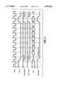
- FIG. 1 is a block diagram of the system.
- FIG. 2 is a timing diagram of the access cycle.
- FIG. 3 is a timing diagram of the data transfer cycle.
- FIG. 1 is an overall view of the additional board, which consists of a data bus 22 and a number of devices, which connect a host processing platform I/O interface bus 21 to a printer 19 to enable the high speed printing of pages having both text and images in the form of graphics or scanned-in pictures.
- the host processing platform I/O interface bus 21 can be connected directly to the printer 19, but many functions, such as compression, decompression, scaling and character image generation are performed slowly by the software in a host processing platform, and high speed printing on the order of 120 pages per minute requires that these functions be performed in special purpose hardware, connected by data bus 22.
- the bus 22 connects through an image storage device 18 to a disk 23, through the image input terminal interface 17 to an input scanner 20, and through an Image output terminal interface 13 to a printer 19.
- the bus 22 is controlled by the bus controller 14, which has its own processor 16 and memory 15.
- the bus 22 is connected to the host bus 21 through the host processing platform I/O interface 11.
- the host platform interface 11 connects the bus 22 to the host processing platform through the host processing platform's native I/O bus interface bus.
- the host processing platform is a Sun Microsystems Computer Corp. SPARCstation.
- the SPARCstation's native I/O interface bus is the "Sbus".
- Image data and control information passes to and from the host processing platform via the interface.
- Imaging accelerator ASIC's are connected to the bus 22. These accelerators receive image data from the bus, process the data according to the function of the particular accelerator, and send the modified image back onto the bus.
- Image data on the bus can originate from the host processing platform, image interface terminal interface or image storage.
- the destination of the image data can be the host processing platform, image output terminal interface, or image storage.
- the image may optionally pass through an imaging accelerator of any kind.
- the movement of data across the bus is coordinated by the bus controller 14.
- This controller drives the control and address lines of the bus; receives the request for data transfer from the imaging accelerators, host bus interface, image storage and I/O devices; arbitrates the request and gives the highest priority request a grant to perform a data transfer on the bus and drives the address and control lines to notify the device sourcing the data and the device sinking the data so that the transfer can take place.
- the bus arbitrates the remaining requests to determine which devices will be granted use of the bus next.
- Programming of the registers in the bus controller and the imaging accelerators is done with an embedded processor 16.
- the current implementation uses an AMD 29200, but any embedded processor could be used.
- Attached to the embedded processor is a memory 15 for stored programs and data.
- the embedded processor does not reside on the bus. Instead, it performs all bus accesses through the controller 14.
- the controller is responsible for the cycle-by-cycle control of the bus.
- the embedded processor is responsible for overall control of the data transfers. This includes initializing devices, programming the source and destinations for image data transfers, setting the priorities for the transfers and performing cleanup after the transfers are complete.
- the bus topology offers a number of important advantages for image manipulation applications. Placing the image accelerators and I/O interface devices on the same bus allows direct transfer of image data from one to the other. This reduces latency and increases throughput.
- the controller 14 Separating the embedded processor from the bus 22 by the controller 14 eliminates embedded processor memory access traffic from the bus. This reduces bus latency and increases bus throughput, but it increases the latency for access by the embedded process to the registers in the imaging accelerators. The drawbacks are outweighed by the improvement in image data transfer since access to the imaging accelerator registers is infrequent compared to image data transfer.
- the separation of the embedded processor from the bus also makes it easy to change the embedded processor to a different family of processors.
- the change of the embedded processor affects only the controller and not the interface of the imaging accelerator devices.
- the bus is unlike many busses in that it does not support random access memory attached directly to the bus.
- the number of address bits is limited and is only sufficient to address the registers in the imaging accelerators and interfaces. Most image data does not have any address information associated with it. If address information must accompany an image, then it is sent as data.
- the bus is a CMOS bus using TTL voltage levels.
- the bus has 32 bits of data and 10 bits of address.
- the address is a byte address; however, the minimum transfer size is one word (32 bits).
- the bus supports two kinds of bus cycles, single word transfers and eight-word transfers. All single-word transfers are to or from the embedded processor. A single-word transfer begins with the embedded processor presenting an address to the controller. The controller will wait until the bus is available and then begin the single-word transfer. The address lines will be driven with the address and one device will have its chip select activated. A single word is either written to or read from the selected bus device.
- An eight-word burst transfer reduces overhead and increases throughput, providing the best balance between the efficiency of large bursts with the FIFO size requirement in each bus device.
- the packet size increases, the overhead from the address cycle becomes a smaller percentage of time spent per bus cycle.
- the disadvantage with very large packet sizes being transferred between ASIC's is that the input and output FIFO's become very large, increasing the cost of the ASIC's.
- the word size is 4 bytes and all burst transfers are 8 words. If an image is not a multiple of eight words, then the last packet must be padded to fill the entire eight words.
- the destination device has the responsibility of separating the padding bytes from the data bytes.
- the protocol does not include any flags or indicators to mark padding bytes.
- the particular embodiment described here has a 32 bit data path and a number of associated control lines, to be discussed below, runs at a clock speed of 16.7 to 25 MHz, is completely synchronous, can handle bursts transfers of data, is compatible with CMOS components, and has a bandwidth of 88M bytes/sec to enable a printing speed of 120 pages per minute, each page containing 4M bytes of data.
- the bus is optimized for CMOS devices using TTL compatible voltage levels, but is not compatible with bipolar devices. It is a chip-level bus, and so the length and loading of the bus is limited.
- the bus is a packet (burst) bus. Burst data transfers across the bus consist of an ID cycle followed by a burst transfer cycle. Exactly eight words are transferred in each packet. This is necessary to get the high throughput required of the bus. All devices on the bus use burst transfers for moving data.
- the bus should be considered a local bus for device interconnect, and therefore does not use parity. It is recommended that the bus devices interfacing to dynamic memory generate and check the parity of the data in the dynamic memory before placing it in the bus.
- the protocol requires two kinds of commands to enable one bulk data transfer, a write or read access cycle and a data transfer cycle.
- the write cycle writes data from the controller to a device
- the read cycle writes data from the device to the controller.
- the original and final locations of the data to be sent must be identified. Since there is a receiving and transmitting device, at least two access commands are required to set up each bulk data transfer.
- a write access cycle begins with the processor presenting an address for accessing to the bus controller.
- the address comprises the chip address, the buffer address in the selected device, and the location of the data in the buffer.
- the controller will enter the request into the arbitration pool for the bus. When the bus becomes available the controller will process the highest priority request as follows.
- the processor will present to the controller an address of a chip. If the address matches a programmed ship select line in the controller, then the controller will put the chip select data on the chip select lines, and set the write, or transfer direction, line. Also, the controller will place the data from the processor onto the data lines. The controller will then wait until the writing of data has been completed, either by waiting a predetermined time period or waiting until the ready line is asserted. If a device fails to respond after 256 clocks, it is considered a timeout and the controller will terminate the bus cycle. At the conclusion of the cycle, the controller will reset the write line and chip select lines, and become ready to receive another command from the processor. The read cycle is the same except that the write line is not asserted and the data moves from the selected device to the processor.
- a data transfer cycle is for the transfer of data directly from one device to another, and has two parts: the ID cycle and the burst transfer cycle.
- the controller For an ID cycle, when the controller has received requests from both a read device and a write device for a transfer between the devices, and the bus is free, the controller will initiate the ID cycle, which lasts for exactly one clock cycle. First, the controller will assert the bus grant line, also referred to as the common DMA acknowledge line, which is monitored by all bus devices except the host platform interface. Next the controller will put a five bit address on the address lines identifying the read device, and another five bit address for the write device. When a device detects that the grant line is asserted, it will compare the read and write ID's to its own. If there is a match, then the device has been granted access to the bus. It must then begin a burst transfer. The read device will also receive the chip select. Only the device receiving the chip select may drive the bus. This prevents bus contention caused by incorrect programming of the bus devices. The host platform interface uses a different protocol for burst transfer.
- the burst transfer automatically follows the ID cycle on the next clock, and lasts exactly eight cycles, one word on each cycle.
Abstract
Description
Claims (1)
Priority Applications (1)
| Application Number | Priority Date | Filing Date | Title |
|---|---|---|---|
| US08/389,612 US5551052A (en) | 1993-08-02 | 1995-02-14 | Data bus protocol for high speed chip to chip data transfer |
Applications Claiming Priority (2)
| Application Number | Priority Date | Filing Date | Title |
|---|---|---|---|
| US10022993A | 1993-08-02 | 1993-08-02 | |
| US08/389,612 US5551052A (en) | 1993-08-02 | 1995-02-14 | Data bus protocol for high speed chip to chip data transfer |
Related Parent Applications (1)
| Application Number | Title | Priority Date | Filing Date |
|---|---|---|---|
| US10022993A Continuation | 1993-08-02 | 1993-08-02 |
Publications (1)
| Publication Number | Publication Date |
|---|---|
| US5551052A true US5551052A (en) | 1996-08-27 |
Family
ID=22278724
Family Applications (1)
| Application Number | Title | Priority Date | Filing Date |
|---|---|---|---|
| US08/389,612 Expired - Lifetime US5551052A (en) | 1993-08-02 | 1995-02-14 | Data bus protocol for high speed chip to chip data transfer |
Country Status (1)
| Country | Link |
|---|---|
| US (1) | US5551052A (en) |
Cited By (6)
| Publication number | Priority date | Publication date | Assignee | Title |
|---|---|---|---|---|
| WO1999021087A1 (en) * | 1997-10-17 | 1999-04-29 | Acuity Imaging, Llc | Flexible processing hardware architecture |
| EP0978787A1 (en) * | 1998-08-04 | 2000-02-09 | Texas Instruments France | Improvements in or relating to transferring data between asynchronous device |
| US6035344A (en) * | 1994-03-25 | 2000-03-07 | Rohm Co., Ltd. | Data transfer apparatus which outputs data based upon a control signal |
| WO2000013095A1 (en) * | 1998-08-28 | 2000-03-09 | Intel Corporation | Method and apparatus for transmitting and receiving network protocol compliant signal packets over a platform bus |
| US20060129725A1 (en) * | 2004-12-09 | 2006-06-15 | Agere Systems Inc. | Round-robin bus protocol |
| CN111522588A (en) * | 2020-04-16 | 2020-08-11 | 珠海泰芯半导体有限公司 | Chip operation interaction method and communication system based on SWD protocol |
Citations (7)
| Publication number | Priority date | Publication date | Assignee | Title |
|---|---|---|---|---|
| US4719621A (en) * | 1985-07-15 | 1988-01-12 | Raytheon Company | Packet fastbus |
| US4805137A (en) * | 1987-01-08 | 1989-02-14 | United Technologies Corporation | Bus controller command block processing system |
| US4992956A (en) * | 1987-10-08 | 1991-02-12 | Advanced Micro Devices, Inc. | Apparatus for assembling data for supply to a scanning output device |
| US5131081A (en) * | 1989-03-23 | 1992-07-14 | North American Philips Corp., Signetics Div. | System having a host independent input/output processor for controlling data transfer between a memory and a plurality of i/o controllers |
| US5179530A (en) * | 1989-11-03 | 1993-01-12 | Zoran Corporation | Architecture for integrated concurrent vector signal processor |
| US5243238A (en) * | 1989-03-17 | 1993-09-07 | Algotronix Limited | Configurable cellular array |
| US5367643A (en) * | 1991-02-06 | 1994-11-22 | International Business Machines Corporation | Generic high bandwidth adapter having data packet memory configured in three level hierarchy for temporary storage of variable length data packets |
-
1995
- 1995-02-14 US US08/389,612 patent/US5551052A/en not_active Expired - Lifetime
Patent Citations (7)
| Publication number | Priority date | Publication date | Assignee | Title |
|---|---|---|---|---|
| US4719621A (en) * | 1985-07-15 | 1988-01-12 | Raytheon Company | Packet fastbus |
| US4805137A (en) * | 1987-01-08 | 1989-02-14 | United Technologies Corporation | Bus controller command block processing system |
| US4992956A (en) * | 1987-10-08 | 1991-02-12 | Advanced Micro Devices, Inc. | Apparatus for assembling data for supply to a scanning output device |
| US5243238A (en) * | 1989-03-17 | 1993-09-07 | Algotronix Limited | Configurable cellular array |
| US5131081A (en) * | 1989-03-23 | 1992-07-14 | North American Philips Corp., Signetics Div. | System having a host independent input/output processor for controlling data transfer between a memory and a plurality of i/o controllers |
| US5179530A (en) * | 1989-11-03 | 1993-01-12 | Zoran Corporation | Architecture for integrated concurrent vector signal processor |
| US5367643A (en) * | 1991-02-06 | 1994-11-22 | International Business Machines Corporation | Generic high bandwidth adapter having data packet memory configured in three level hierarchy for temporary storage of variable length data packets |
Cited By (13)
| Publication number | Priority date | Publication date | Assignee | Title |
|---|---|---|---|---|
| US6035344A (en) * | 1994-03-25 | 2000-03-07 | Rohm Co., Ltd. | Data transfer apparatus which outputs data based upon a control signal |
| WO1999021087A1 (en) * | 1997-10-17 | 1999-04-29 | Acuity Imaging, Llc | Flexible processing hardware architecture |
| US6636907B1 (en) | 1998-08-04 | 2003-10-21 | Texas Instruments Incorporated | Transferring data between asynchronous devices |
| EP0978787A1 (en) * | 1998-08-04 | 2000-02-09 | Texas Instruments France | Improvements in or relating to transferring data between asynchronous device |
| US20040202161A1 (en) * | 1998-08-28 | 2004-10-14 | Stachura Thomas L. | Method and apparatus for transmitting and receiving network protocol compliant signal packets over a platform bus |
| US6754209B1 (en) | 1998-08-28 | 2004-06-22 | Intel Corporation | Method and apparatus for transmitting and receiving network protocol compliant signal packets over a platform bus |
| WO2000013095A1 (en) * | 1998-08-28 | 2000-03-09 | Intel Corporation | Method and apparatus for transmitting and receiving network protocol compliant signal packets over a platform bus |
| US20060129725A1 (en) * | 2004-12-09 | 2006-06-15 | Agere Systems Inc. | Round-robin bus protocol |
| US7350002B2 (en) | 2004-12-09 | 2008-03-25 | Agere Systems, Inc. | Round-robin bus protocol |
| US20080126640A1 (en) * | 2004-12-09 | 2008-05-29 | Agere Systems Inc. | Round-Robin Bus Protocol |
| US7698485B2 (en) | 2004-12-09 | 2010-04-13 | Agere Systems Inc. | Round-robin bus protocol |
| CN111522588A (en) * | 2020-04-16 | 2020-08-11 | 珠海泰芯半导体有限公司 | Chip operation interaction method and communication system based on SWD protocol |
| CN111522588B (en) * | 2020-04-16 | 2023-05-05 | 珠海泰芯半导体有限公司 | Chip operation interaction method and communication system based on SWD protocol |
Similar Documents
| Publication | Publication Date | Title |
|---|---|---|
| US6629179B1 (en) | Message signaled interrupt generating device and method | |
| EP0392657B1 (en) | System providing cache coherent direct memory access between dissimilar bus systems | |
| US4602327A (en) | Bus master capable of relinquishing bus on request and retrying bus cycle | |
| US5426737A (en) | Direct memory access for data transfer within an I/O device | |
| JPH0713908A (en) | Method and apparatus for provision of back- to-back data transfer in information- processing system with multiplex bus | |
| US6889266B1 (en) | Method for delivering packet boundary or other metadata to and from a device using direct memory controller | |
| KR19980081526A (en) | PCI bus system | |
| US6766386B2 (en) | Method and interface for improved efficiency in performing bus-to-bus read data transfers | |
| US5481681A (en) | Data transfer operations between two asynchronous buses | |
| EP0464848A2 (en) | Structure for enabling direct memory-to-memory transfer | |
| JPH09160866A (en) | Bus interface logic system and synchronization method | |
| US5414814A (en) | I/O interface between VME bus and asynchronous serial data computer | |
| US5551052A (en) | Data bus protocol for high speed chip to chip data transfer | |
| EP0784278B1 (en) | Interface architecture for connection to a peripheral component interconnect bus | |
| US5799161A (en) | Method and apparatus for concurrent data routing | |
| EP0690382B1 (en) | Computer system with a multiplexed address bus and pipelined write operations | |
| JPS6242306B2 (en) | ||
| JPH10178626A (en) | Transmitting device, server device and transmitting method | |
| JP2003316724A (en) | Signal transmission device between control chip sets | |
| EP0691616A1 (en) | RAM and ROM control unit | |
| JP3304395B2 (en) | Data transfer device and data transfer method | |
| JP2963696B2 (en) | Data transfer control system | |
| JPH06250965A (en) | Input/output controller | |
| JP2790668B2 (en) | Data transfer control method | |
| JPH06119289A (en) | Data transfer device |
Legal Events
| Date | Code | Title | Description |
|---|---|---|---|
| STCF | Information on status: patent grant |
Free format text: PATENTED CASE |
|
| FPAY | Fee payment |
Year of fee payment: 4 |
|
| AS | Assignment |
Owner name: BANK ONE, NA, AS ADMINISTRATIVE AGENT, ILLINOIS Free format text: SECURITY INTEREST;ASSIGNOR:XEROX CORPORATION;REEL/FRAME:013153/0001 Effective date: 20020621 |
|
| AS | Assignment |
Owner name: JPMORGAN CHASE BANK, AS COLLATERAL AGENT, TEXAS Free format text: SECURITY AGREEMENT;ASSIGNOR:XEROX CORPORATION;REEL/FRAME:015134/0476 Effective date: 20030625 Owner name: JPMORGAN CHASE BANK, AS COLLATERAL AGENT,TEXAS Free format text: SECURITY AGREEMENT;ASSIGNOR:XEROX CORPORATION;REEL/FRAME:015134/0476 Effective date: 20030625 |
|
| FPAY | Fee payment |
Year of fee payment: 8 |
|
| FPAY | Fee payment |
Year of fee payment: 12 |
|
| AS | Assignment |
Owner name: XEROX CORPORATION, CONNECTICUT Free format text: RELEASE BY SECURED PARTY;ASSIGNOR:JPMORGAN CHASE BANK, N.A. AS SUCCESSOR-IN-INTEREST ADMINISTRATIVE AGENT AND COLLATERAL AGENT TO JPMORGAN CHASE BANK;REEL/FRAME:066728/0193 Effective date: 20220822 |