US5574868A - Bus grant prediction technique for a split transaction bus in a multiprocessor computer system - Google Patents
Bus grant prediction technique for a split transaction bus in a multiprocessor computer system Download PDFInfo
- Publication number
- US5574868A US5574868A US08/062,065 US6206593A US5574868A US 5574868 A US5574868 A US 5574868A US 6206593 A US6206593 A US 6206593A US 5574868 A US5574868 A US 5574868A
- Authority
- US
- United States
- Prior art keywords
- data
- memory
- bus
- communication bus
- data communication
- Prior art date
- Legal status (The legal status is an assumption and is not a legal conclusion. Google has not performed a legal analysis and makes no representation as to the accuracy of the status listed.)
- Expired - Lifetime
Links
Images

Classifications
-
- G—PHYSICS
- G06—COMPUTING; CALCULATING OR COUNTING
- G06F—ELECTRIC DIGITAL DATA PROCESSING
- G06F13/00—Interconnection of, or transfer of information or other signals between, memories, input/output devices or central processing units
- G06F13/14—Handling requests for interconnection or transfer
- G06F13/36—Handling requests for interconnection or transfer for access to common bus or bus system
- G06F13/362—Handling requests for interconnection or transfer for access to common bus or bus system with centralised access control
-
- G—PHYSICS
- G06—COMPUTING; CALCULATING OR COUNTING
- G06F—ELECTRIC DIGITAL DATA PROCESSING
- G06F13/00—Interconnection of, or transfer of information or other signals between, memories, input/output devices or central processing units
- G06F13/14—Handling requests for interconnection or transfer
- G06F13/16—Handling requests for interconnection or transfer for access to memory bus
- G06F13/18—Handling requests for interconnection or transfer for access to memory bus based on priority control
Definitions
- This invention relates generally to the field of data communications within a multiprocessor computer system, and particularly to a technique for optimizing the memory response time of a shared memory system utilizing a split transaction bus for burst data transfers.
- Modern data processing systems typically include a main memory system constructed with dynamic random access memory (DRAM) devices.
- the main memory system communicates by way of a memory bus or system bus with other agents of the system such as processors and direct memory access (DMA) masters.
- DMA direct memory access
- a memory controller directs data into and out of the main memory system.
- High performance systems with multiple processing units require a greater bandwidth on the memory bus to handle the multiple memory access requests generated by the multiple processing units.
- One technique for increasing the effective bus bandwidth required in multiprocessor systems is the use of a split transaction bus.
- a split transaction an agent of the system requests a memory access, thereby initiating a transaction, and the transaction is completed when the requested data is supplied by the memory system.
- the memory bus is available for other transactions. While this technique increases the effective bandwidth of the memory bus, it does so at the expense of longer latencies. If a multiprocessor system is configured with only a single processor, a split transaction bus actually degrades performance of the system due to the increased latencies which could be avoided by using a simple shared memory bus.
- a multiprocessor system will frequently operate in a uniprocessor mode.
- a system that is multiprocessor (MP) ready for OS/2 or UNIX will operate in a uniprocessor mode when running DOS. Therefore, it is desirable that a multiprocessor system be designed to optimize bus performance in a uniprocessor mode as well as a multiprocessor mode.
- FIG. 1 illustrates the sequence of events for a single transaction on a simple shared memory bus.
- a read request is issued by a requesting agent and transmitted on the memory bus.
- the request is received by the memory controller and decoded to generate the control signals that retrieve the requested data from the memory.
- the data is then transmitted on the memory bus to the requesting agent.
- the bus is occupied for the entire time of the transaction from the initiation of the read request to the completion of the data transmission. No bus arbitration is required since the bus is owned by the requesting and responding agents for the duration of the transaction. Thus, access to the bus is denied to all other agents in the system.
- FIG. 2 Operation of a typical split transaction bus is illustrated in FIG. 2.
- a transaction is similarly initiated by a read request from a requesting agent.
- the read request is received by the memory controller which decodes the request and generates the memory access control signals.
- the split transaction bus is occupied only during the time that the read request is transmitted. The bus is then made available to other agents while the request is decoded and requested data is retrieved from the memory. The retrieved data is typically stored in a first in, first out (FIFO) data buffer until the bus is again available to transmit the data to the requesting agent.
- FIFO first in, first out
- bus arbitration and grant sequence arbitrates active bus access requests from other requesting and responding agents and then assigns the bus to the responding agent to transmit the data to the requesting agent.
- bus availability is increased, but memory response latency is also increased due to the sequential nature of the memory read, memory bus arbitration, bus grant and data transmission operations.
- increase in latency could be avoided by sending the accessed data directly onto the memory bus as it is retrieved from the memory; however, this would require that access to the bus be denied to other agents prior to and during the time that the data is retrieved in order to avoid bus collisions. Such an approach would therefore negate most of the increase in bandwidth achievable with the split transaction technique.
- the present invention combines the operating advantages of both a split transaction bus and a simple shared bus by implementing an early bus grant prediction technique.
- an early bus request is generated for the impending data transfer.
- the early bus request is provided to bus grant prediction and arbitration logic that determines whether or not the bus will be available at the time the requested data has been retrieved and is ready for transfer. If the bus is available, the retrieved data is routed immediately to the memory bus for a fly-by transfer. On the other hand, if the bus is not available, the data is routed to a FIFO buffer to be transferred when the bus becomes available.
- the bus appears to the memory system as a simple shared bus since fly-by transfers will always be performed.
- the bus will also appear to the memory system as a simple shared bus.
- the bus appears to the memory system as a conventional split transaction bus.
- FIG. 1 illustrates a memory access transaction in a prior art simple shared bus.
- FIG. 2 illustrates a memory access transaction in a prior art split transaction bus.
- FIG. 3 is a block diagram of a memory system according to the present invention.
- FIG. 4 illustrates a memory access transaction implemented by the present invention.
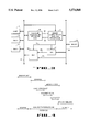
- FIG. 3 is a functional block diagram of a memory system that combines the operating advantages of a split transaction bus and a simple shared bus.
- a high speed split transaction system bus 10 connects a plurality of system agents 12, including one or more processing units.
- a memory read request is transmitted by one of the system agents to memory controller 14.
- the read request is decoded by controller 14 and transmitted to memory 16 on memory bus 18.
- memory controller 14 follows a decoding sequence of the read request, memory controller 14 knows the memory access latency in a deterministic fashion. While the memory access is in progress, memory controller 14 sends an early bus request signal on line 20 to prediction and arbitration logic unit 22.
- Prediction and arbitration logic unit 22 includes a bus occupation state machine that tracks the ownership and arbitration status of system bus 10.
- the bus occupation state machine predicts bus status up to seven clocks ahead and has the following states:
- DI Data bus unused this clock, available next clock
- D7 Data bus busy this and the next 7 clocks, allow one dead clock
- D6 Data bus busy this and the next 6 clocks, allow one dead clock
- D5 Data bus busy this and the next 5 clocks, allow one dead clock
- D4 Data bus busy this and the next 4 clocks, allow one dead clock
- D3 Data bus busy this and the next 3 clocks, allow one dead clock
- D2 Data bus busy this and the next 2 clocks, allow one dead clock
- D1 Data bus busy this and the next 1 clock, allow one dead clock
- prediction logic in unit 22 Upon receiving an early bus request signal from memory controller 14, prediction logic in unit 22, based on information from the bus occupation state machine, returns appropriate bus grant status signals on line 24 to memory controller 14. These signals inform the memory controller of the exact time when system bus 10 will be available for data transmission.
- memory controller 14 Based on the information provided by the bus grant status signals, memory controller 14 is informed as to whether or not system bus 10 will be available at the time the requested data is retrieved from memory 16 and placed on memory bus 18. If it is known that the system bus will be available, the data is routed directly to system bus 10 through multiplexer 26. Control signals on line 28 from memory controller 14 select multiplexer input 27a to route the data onto the system bus for a "fly-by" transfer.
- the early bus request is generated by memory controller 14 as it decodes the read request from the requesting agent.
- Prediction and arbitration logic unit 22 responds with bus grant status signals while the access to memory 16 is in process.
- the bus arbitration permits transmission of the data onto system bus 10 immediately upon completion of the memory access. Had it been determined in the state machine of unit 22 that system bus 10 would not be available when the memory access was completed, the bus arbitration phase would extend until the bus became available for the data transfer.
Abstract
Description
Claims (11)
Priority Applications (1)
| Application Number | Priority Date | Filing Date | Title |
|---|---|---|---|
| US08/062,065 US5574868A (en) | 1993-05-14 | 1993-05-14 | Bus grant prediction technique for a split transaction bus in a multiprocessor computer system |
Applications Claiming Priority (1)
| Application Number | Priority Date | Filing Date | Title |
|---|---|---|---|
| US08/062,065 US5574868A (en) | 1993-05-14 | 1993-05-14 | Bus grant prediction technique for a split transaction bus in a multiprocessor computer system |
Publications (1)
| Publication Number | Publication Date |
|---|---|
| US5574868A true US5574868A (en) | 1996-11-12 |
Family
ID=22039996
Family Applications (1)
| Application Number | Title | Priority Date | Filing Date |
|---|---|---|---|
| US08/062,065 Expired - Lifetime US5574868A (en) | 1993-05-14 | 1993-05-14 | Bus grant prediction technique for a split transaction bus in a multiprocessor computer system |
Country Status (1)
| Country | Link |
|---|---|
| US (1) | US5574868A (en) |
Cited By (26)
| Publication number | Priority date | Publication date | Assignee | Title |
|---|---|---|---|---|
| US5768544A (en) * | 1996-09-26 | 1998-06-16 | Intel Corporation | Deterministic latency characterization and mitigation |
| FR2772969A1 (en) * | 1997-12-24 | 1999-06-25 | Thomson Multimedia Sa | Management system for random access memories |
| US5933610A (en) * | 1996-09-17 | 1999-08-03 | Vlsi Technology, Inc. | Predictive arbitration system for PCI bus agents |
| US5982672A (en) * | 1996-10-18 | 1999-11-09 | Samsung Electronics Co., Ltd. | Simultaneous data transfer through read and write buffers of a DMA controller |
| US6065077A (en) * | 1997-12-07 | 2000-05-16 | Hotrail, Inc. | Apparatus and method for a cache coherent shared memory multiprocessing system |
| US6065093A (en) * | 1998-05-15 | 2000-05-16 | International Business Machines Corporation | High bandwidth narrow I/O memory device with command stacking |
| US6098133A (en) * | 1997-11-28 | 2000-08-01 | Motorola, Inc. | Secure bus arbiter interconnect arrangement |
| US6105082A (en) * | 1997-05-15 | 2000-08-15 | Ricoh Company, Ltd. | Data processor used in a data transfer system which includes a detection circuit for detecting whether processor uses bus in a forthcoming cycle |
| US6173349B1 (en) * | 1996-10-18 | 2001-01-09 | Samsung Electronics Co., Ltd. | Shared bus system with transaction and destination ID |
| US6292705B1 (en) | 1998-09-29 | 2001-09-18 | Conexant Systems, Inc. | Method and apparatus for address transfers, system serialization, and centralized cache and transaction control, in a symetric multiprocessor system |
| US6418537B1 (en) | 1997-12-07 | 2002-07-09 | Conexant Systems, Inc. | Accurate timing calibration for each of multiple high-speed clocked receivers using a single DLL |
| WO2002054261A1 (en) | 2000-12-28 | 2002-07-11 | Koninklijke Philips Electronics N.V. | System integrating agents having different resource-accessing schemes |
| US6469988B1 (en) | 1999-07-08 | 2002-10-22 | Conexant Systems, Inc. | Low-level circuit implementation of signal flow graphs for real-time signal processing of high-speed digital signals |
| US6516442B1 (en) | 1997-12-07 | 2003-02-04 | Conexant Systems, Inc. | Channel interface and protocols for cache coherency in a scalable symmetric multiprocessor system |
| US6516375B1 (en) | 1999-11-03 | 2003-02-04 | Intel Corporation | Peripheral component interconnect (PCI) configuration emulation for hub interface |
| WO2003034243A1 (en) * | 2001-10-16 | 2003-04-24 | Koninklijke Philips Electronics N.V. | A computer system with a communication bus |
| US6633945B1 (en) | 1997-12-07 | 2003-10-14 | Conexant Systems, Inc. | Fully connected cache coherent multiprocessing systems |
| US20040221075A1 (en) * | 2001-08-28 | 2004-11-04 | Broadcom Corporation | Method and interface for improved efficiency in performing bus-to-bus read data transfers |
| US20040267992A1 (en) * | 2002-02-28 | 2004-12-30 | Stuber Russell B | Look ahead split release for a data bus |
| US20050060452A1 (en) * | 2003-09-02 | 2005-03-17 | Intel Corporation | System and method for generating bus requests in advance based on speculation states |
| US20060206645A1 (en) * | 2004-06-08 | 2006-09-14 | Arm Limited | Performing arbitration in a data processing apparatus |
| US20070073977A1 (en) * | 2005-09-29 | 2007-03-29 | Safranek Robert J | Early global observation point for a uniprocessor system |
| US20090013115A1 (en) * | 2007-07-03 | 2009-01-08 | Kouichi Ishino | Bus communication apparatus that uses shared memory |
| US20090253495A1 (en) * | 2008-04-02 | 2009-10-08 | Wms Gaming Inc. | Gaming machines with normalized power consumption |
| US7966439B1 (en) * | 2004-11-24 | 2011-06-21 | Nvidia Corporation | Apparatus, system, and method for a fast data return memory controller |
| US9135195B2 (en) | 2012-07-24 | 2015-09-15 | Freescasle Semiconductor, Inc. | Prediction of electronic component behavior in bus-based systems |
Citations (8)
| Publication number | Priority date | Publication date | Assignee | Title |
|---|---|---|---|---|
| US4159532A (en) * | 1977-08-04 | 1979-06-26 | Honeywell Information Systems Inc. | FIFO look-ahead system |
| US4757439A (en) * | 1984-11-02 | 1988-07-12 | Measurex Corporation | Memory bus architecture |
| US4792926A (en) * | 1985-12-09 | 1988-12-20 | Kabushiki Kaisha Toshiba | High speed memory system for use with a control bus bearing contiguous segmentially intermixed data read and data write request signals |
| US4980854A (en) * | 1987-05-01 | 1990-12-25 | Digital Equipment Corporation | Lookahead bus arbitration system with override of conditional access grants by bus cycle extensions for multicycle data transfers |
| US5032985A (en) * | 1988-07-21 | 1991-07-16 | International Business Machines Corporation | Multiprocessor system with memory fetch buffer invoked during cross-interrogation |
| US5278974A (en) * | 1989-12-04 | 1994-01-11 | Digital Equipment Corporation | Method and apparatus for the dynamic adjustment of data transfer timing to equalize the bandwidths of two buses in a computer system having different bandwidths |
| US5297292A (en) * | 1990-05-11 | 1994-03-22 | Hitachi, Ltd. | Bus system wherein a bus-using request signal is issued in advance of a determination that a bus is to be used and is thereafter cancelled if the bus is not used |
| US5440698A (en) * | 1990-11-30 | 1995-08-08 | Xerox Corporation | Arbitration of packet switched busses, including busses for shared memory multiprocessors |
-
1993
- 1993-05-14 US US08/062,065 patent/US5574868A/en not_active Expired - Lifetime
Patent Citations (8)
| Publication number | Priority date | Publication date | Assignee | Title |
|---|---|---|---|---|
| US4159532A (en) * | 1977-08-04 | 1979-06-26 | Honeywell Information Systems Inc. | FIFO look-ahead system |
| US4757439A (en) * | 1984-11-02 | 1988-07-12 | Measurex Corporation | Memory bus architecture |
| US4792926A (en) * | 1985-12-09 | 1988-12-20 | Kabushiki Kaisha Toshiba | High speed memory system for use with a control bus bearing contiguous segmentially intermixed data read and data write request signals |
| US4980854A (en) * | 1987-05-01 | 1990-12-25 | Digital Equipment Corporation | Lookahead bus arbitration system with override of conditional access grants by bus cycle extensions for multicycle data transfers |
| US5032985A (en) * | 1988-07-21 | 1991-07-16 | International Business Machines Corporation | Multiprocessor system with memory fetch buffer invoked during cross-interrogation |
| US5278974A (en) * | 1989-12-04 | 1994-01-11 | Digital Equipment Corporation | Method and apparatus for the dynamic adjustment of data transfer timing to equalize the bandwidths of two buses in a computer system having different bandwidths |
| US5297292A (en) * | 1990-05-11 | 1994-03-22 | Hitachi, Ltd. | Bus system wherein a bus-using request signal is issued in advance of a determination that a bus is to be used and is thereafter cancelled if the bus is not used |
| US5440698A (en) * | 1990-11-30 | 1995-08-08 | Xerox Corporation | Arbitration of packet switched busses, including busses for shared memory multiprocessors |
Cited By (34)
| Publication number | Priority date | Publication date | Assignee | Title |
|---|---|---|---|---|
| US5933610A (en) * | 1996-09-17 | 1999-08-03 | Vlsi Technology, Inc. | Predictive arbitration system for PCI bus agents |
| US5768544A (en) * | 1996-09-26 | 1998-06-16 | Intel Corporation | Deterministic latency characterization and mitigation |
| US6173349B1 (en) * | 1996-10-18 | 2001-01-09 | Samsung Electronics Co., Ltd. | Shared bus system with transaction and destination ID |
| US5982672A (en) * | 1996-10-18 | 1999-11-09 | Samsung Electronics Co., Ltd. | Simultaneous data transfer through read and write buffers of a DMA controller |
| US6105082A (en) * | 1997-05-15 | 2000-08-15 | Ricoh Company, Ltd. | Data processor used in a data transfer system which includes a detection circuit for detecting whether processor uses bus in a forthcoming cycle |
| US6098133A (en) * | 1997-11-28 | 2000-08-01 | Motorola, Inc. | Secure bus arbiter interconnect arrangement |
| US6065077A (en) * | 1997-12-07 | 2000-05-16 | Hotrail, Inc. | Apparatus and method for a cache coherent shared memory multiprocessing system |
| US6418537B1 (en) | 1997-12-07 | 2002-07-09 | Conexant Systems, Inc. | Accurate timing calibration for each of multiple high-speed clocked receivers using a single DLL |
| US6633945B1 (en) | 1997-12-07 | 2003-10-14 | Conexant Systems, Inc. | Fully connected cache coherent multiprocessing systems |
| US6457087B1 (en) | 1997-12-07 | 2002-09-24 | Conexant Systems, Inc. | Apparatus and method for a cache coherent shared memory multiprocessing system |
| US6516442B1 (en) | 1997-12-07 | 2003-02-04 | Conexant Systems, Inc. | Channel interface and protocols for cache coherency in a scalable symmetric multiprocessor system |
| FR2772969A1 (en) * | 1997-12-24 | 1999-06-25 | Thomson Multimedia Sa | Management system for random access memories |
| US6065093A (en) * | 1998-05-15 | 2000-05-16 | International Business Machines Corporation | High bandwidth narrow I/O memory device with command stacking |
| US6292705B1 (en) | 1998-09-29 | 2001-09-18 | Conexant Systems, Inc. | Method and apparatus for address transfers, system serialization, and centralized cache and transaction control, in a symetric multiprocessor system |
| US6466825B1 (en) | 1998-09-29 | 2002-10-15 | Conexant Systems, Inc. | Method and apparatus for address transfers, system serialization, and centralized cache and transaction control, in a symetric multiprocessor system |
| US6469988B1 (en) | 1999-07-08 | 2002-10-22 | Conexant Systems, Inc. | Low-level circuit implementation of signal flow graphs for real-time signal processing of high-speed digital signals |
| US6516375B1 (en) | 1999-11-03 | 2003-02-04 | Intel Corporation | Peripheral component interconnect (PCI) configuration emulation for hub interface |
| WO2002054261A1 (en) | 2000-12-28 | 2002-07-11 | Koninklijke Philips Electronics N.V. | System integrating agents having different resource-accessing schemes |
| US20040221075A1 (en) * | 2001-08-28 | 2004-11-04 | Broadcom Corporation | Method and interface for improved efficiency in performing bus-to-bus read data transfers |
| WO2003034243A1 (en) * | 2001-10-16 | 2003-04-24 | Koninklijke Philips Electronics N.V. | A computer system with a communication bus |
| CN1318993C (en) * | 2001-10-16 | 2007-05-30 | 皇家飞利浦电子股份有限公司 | Computer system with a communication bus |
| US7174401B2 (en) * | 2002-02-28 | 2007-02-06 | Lsi Logic Corporation | Look ahead split release for a data bus |
| US20040267992A1 (en) * | 2002-02-28 | 2004-12-30 | Stuber Russell B | Look ahead split release for a data bus |
| US20050060452A1 (en) * | 2003-09-02 | 2005-03-17 | Intel Corporation | System and method for generating bus requests in advance based on speculation states |
| US20060265532A1 (en) * | 2003-09-02 | 2006-11-23 | Intel Corporation | System and method for generating bus requests in advance based on speculation states |
| US7099968B2 (en) * | 2003-09-02 | 2006-08-29 | Intel Corporation | System and method for generating bus requests in advance based on speculation states |
| US20060206645A1 (en) * | 2004-06-08 | 2006-09-14 | Arm Limited | Performing arbitration in a data processing apparatus |
| US7290075B2 (en) * | 2004-06-08 | 2007-10-30 | Arm Limited | Performing arbitration in a data processing apparatus |
| US7966439B1 (en) * | 2004-11-24 | 2011-06-21 | Nvidia Corporation | Apparatus, system, and method for a fast data return memory controller |
| US20070073977A1 (en) * | 2005-09-29 | 2007-03-29 | Safranek Robert J | Early global observation point for a uniprocessor system |
| US20090013115A1 (en) * | 2007-07-03 | 2009-01-08 | Kouichi Ishino | Bus communication apparatus that uses shared memory |
| US7774529B2 (en) * | 2007-07-03 | 2010-08-10 | Panasonic Corporation | Bus communication apparatus that uses shared memory |
| US20090253495A1 (en) * | 2008-04-02 | 2009-10-08 | Wms Gaming Inc. | Gaming machines with normalized power consumption |
| US9135195B2 (en) | 2012-07-24 | 2015-09-15 | Freescasle Semiconductor, Inc. | Prediction of electronic component behavior in bus-based systems |
Similar Documents
| Publication | Publication Date | Title |
|---|---|---|
| US5574868A (en) | Bus grant prediction technique for a split transaction bus in a multiprocessor computer system | |
| US5003465A (en) | Method and apparatus for increasing system throughput via an input/output bus and enhancing address capability of a computer system during DMA read/write operations between a common memory and an input/output device | |
| US4481572A (en) | Multiconfigural computers utilizing a time-shared bus | |
| US5850530A (en) | Method and apparatus for improving bus efficiency by enabling arbitration based upon availability of completion data | |
| KR100255551B1 (en) | A method and an apparatus for enabling a processor to access an external component through a private bus or a shared bus | |
| US5590299A (en) | Multiprocessor system bus protocol for optimized accessing of interleaved storage modules | |
| JPS63269247A (en) | Memory control subsystem | |
| US5313591A (en) | Computer bus arbitration for N processors requiring only N unidirectional signal leads | |
| JPH0219945A (en) | Main memory controller | |
| JP2532191B2 (en) | A method of managing data transmission for use in a computing system having a dual bus architecture. | |
| US5944805A (en) | System and method for transmitting data upon an address portion of a computer system bus during periods of maximum utilization of a data portion of the bus | |
| KR100347473B1 (en) | Fast pipelined distributed arbitration scheme | |
| US6247101B1 (en) | Tagged access synchronous bus architecture | |
| JP2591502B2 (en) | Information processing system and its bus arbitration system | |
| JP2734246B2 (en) | Pipeline bus | |
| US6195721B1 (en) | Inter-processor data transfer management | |
| US5826045A (en) | Arbitration parking apparatus and method for a split transaction bus in a multiprocessor computer system | |
| KR100266883B1 (en) | Low latency first data access in a data buffered smp memory controller | |
| US5815676A (en) | Address bus arbiter for pipelined transactions on a split bus | |
| JP2002024007A (en) | Processor system | |
| JP3110024B2 (en) | Memory control system | |
| EP0533429B1 (en) | Computer bus control system | |
| KR950004249B1 (en) | Method for data transmission between host and node computers of parallel processing system | |
| JP2682789B2 (en) | Computer I / O cache system | |
| JPH1139266A (en) | Multiprocessor device |
Legal Events
| Date | Code | Title | Description |
|---|---|---|---|
| AS | Assignment |
Owner name: INTEL CORPORATION, CALIFORNIA Free format text: ASSIGNMENT OF ASSIGNORS INTEREST;ASSIGNOR:MARISETTY, SURESH;REEL/FRAME:006567/0917 Effective date: 19930513 |
|
| STPP | Information on status: patent application and granting procedure in general |
Free format text: APPLICATION UNDERGOING PREEXAM PROCESSING |
|
| FEPP | Fee payment procedure |
Free format text: PAYOR NUMBER ASSIGNED (ORIGINAL EVENT CODE: ASPN); ENTITY STATUS OF PATENT OWNER: LARGE ENTITY |
|
| FPAY | Fee payment |
Year of fee payment: 4 |
|
| FPAY | Fee payment |
Year of fee payment: 8 |
|
| FEPP | Fee payment procedure |
Free format text: PAYER NUMBER DE-ASSIGNED (ORIGINAL EVENT CODE: RMPN); ENTITY STATUS OF PATENT OWNER: LARGE ENTITY Free format text: PAYOR NUMBER ASSIGNED (ORIGINAL EVENT CODE: ASPN); ENTITY STATUS OF PATENT OWNER: LARGE ENTITY |
|
| FPAY | Fee payment |
Year of fee payment: 12 |