US5579299A - Communications network, a dual mode data transfer system therefor - Google Patents
Communications network, a dual mode data transfer system therefor Download PDFInfo
- Publication number
- US5579299A US5579299A US08/357,002 US35700294A US5579299A US 5579299 A US5579299 A US 5579299A US 35700294 A US35700294 A US 35700294A US 5579299 A US5579299 A US 5579299A
- Authority
- US
- United States
- Prior art keywords
- mcu
- bus
- byte
- link apparatus
- spi
- Prior art date
- Legal status (The legal status is an assumption and is not a legal conclusion. Google has not performed a legal analysis and makes no representation as to the accuracy of the status listed.)
- Expired - Lifetime
Links
Images


Classifications
-
- H—ELECTRICITY
- H04—ELECTRIC COMMUNICATION TECHNIQUE
- H04L—TRANSMISSION OF DIGITAL INFORMATION, e.g. TELEGRAPHIC COMMUNICATION
- H04L12/00—Data switching networks
- H04L12/28—Data switching networks characterised by path configuration, e.g. LAN [Local Area Networks] or WAN [Wide Area Networks]
- H04L12/40—Bus networks
- H04L12/407—Bus networks with decentralised control
- H04L12/413—Bus networks with decentralised control with random access, e.g. carrier-sense multiple-access with collision detection (CSMA-CD)
- H04L12/4135—Bus networks with decentralised control with random access, e.g. carrier-sense multiple-access with collision detection (CSMA-CD) using bit-wise arbitration
-
- F—MECHANICAL ENGINEERING; LIGHTING; HEATING; WEAPONS; BLASTING
- F02—COMBUSTION ENGINES; HOT-GAS OR COMBUSTION-PRODUCT ENGINE PLANTS
- F02B—INTERNAL-COMBUSTION PISTON ENGINES; COMBUSTION ENGINES IN GENERAL
- F02B75/00—Other engines
- F02B75/02—Engines characterised by their cycles, e.g. six-stroke
- F02B2075/022—Engines characterised by their cycles, e.g. six-stroke having less than six strokes per cycle
- F02B2075/027—Engines characterised by their cycles, e.g. six-stroke having less than six strokes per cycle four
Definitions
- This invention relates to communication over a multiplex data communications network.
- this invention relates to a system for interchanging data bytes within a node between a microcontroller (MCU) and a first peripheral at a chosen clock frequency. Then within the same node, the first peripheral generates a protocol bit and then converts both the protocol bit and each bit of the data bytes from the MCU into variable pulse width modulated (VPWM) bits forming a VPWM message.
- MCU microcontroller
- VPWM variable pulse width modulated
- the first peripheral After forming the message of VPWM bits, the first peripheral sends the VPWM bits to a second peripheral that converts each VPWM bit into a communications symbol (known as a J1850 symbol) conforming to the communication requirements of the Society of Automotive Engineers (SAE) established Recommended Practice J1850 (a set of technical requirements and parameters).
- SAE Society of Automotive Engineers
- the second peripheral drives these symbols onto a single-wire communications bus to communicate the message to other nodes connected to the bus.
- the second peripheral also routes a reflection of the symbols back to the first peripheral and reconverts the symbols into VPWM bits.
- the first peripheral than reassembling the reflected bits into bytes used in the next interchange of bytes with the MCU and to check for the achievement of arbitration if other nodes on the bus are transmitting.
- That search ended in the present invention which accomplishes reducing the time restraints required to process the data prior to converting the data into J1850 symbols and for determining whether a node has gained control of the bus by winning an arbitration contest with competing nodes during a message frame.
- the present invention discloses using a conventional serial peripheral interface (SPI) transfer circuit within the MCU to communicate with a serial peripheral data register (LSPDR) in a peripheral referred to as a link device (Link).
- SPI serial peripheral interface
- LSPDR serial peripheral data register
- Link device Link device
- the individual bits of the SPI-XFRed byte are converted to variable pulse width modulated bits and are then driven onto the bus by an integrated driver/receiver (IDR) module as J1850 symbols at the chosen clock rate but delayed to compensate for the variations in pulse width of each symbol, e.g., one symbol may be longer than another (64 or 128 ⁇ s long). Hence 64 clock pulses would occur during the transfer of a 64 ⁇ s long symbol.
- the ratio of SPI transfer to bus transfer are such that a period of time, illustratively 500 ⁇ s, may result between SPI-XFRs of individual bytes, removing the need for interrupts.
- the system however, contains the capability of operating in an interrupt mode.
- IDR integrated driver receiver circuit
- Clock signal clocks bits of data bytes through circuits within the MCU at a fixed clock frequency while shift clock (SHCLK), clock (CLK) and clock divide by 2 (C1KDIV2) and clock circuits within the Link and IDR during transfers of VPWM bits and symbols
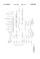
- FIG. 1 illustrates in block diagram form a communications network employing the dual-stage data transfer system of this invention in each node of the network;
- FIG. 2 depicts in expanded block diagram form to show the components of the Link in a pair of nodes of FIG. 1 connected to the communication bus;
- FIGS. 3, 4 and 5 illustrate in partial block and logic diagram form the transmitter/receiver, the transmitter and receiver circuits, respectively, of the symbol encoder/decoder modified to interface and form a part of the Link;
- FIG. 6A-6G depict significant timing sequences associated with the operation of the SPI-XFR system
- FIG. 7A-7J illustrate timing diagrams associated with transferring a three-byte message from the MCU to the Link and over the single-wire bus to other nodes of the network;
- FIG. 8 illustrates a state diagram of the various states required to transfer byte messages from the MCU to the bus and for checking arbitration of symbols on the bus;
- FIG. 9A-9C illustrates in partial block and partial logic diagram form the devices in Link used to exchange data bytes with the MCU and to send to and receive from the bus data symbols;
- FIGS. 10A-10C depict the flowchart of the firmware programs for controlling the operation of the MCU during solicited and unsolicited SPI-XFRs of data bytes.
- FIG. 1 depicts a block diagram of a communications network 10 with several nodes 16a-16f coupled between a single-wire bus 12 and a plurality of sensors or application devices 14a-14f.
- the nodes include MCUs 18a-18f and Links 22a-22f circuits and interfaces for performing SPI-XFRs, and IDRs 20a-20f connected to the Links for converting between digital pulses and J1850 symbols during sending and receiving messages over bus 12.
- Each Link 22 interconnects between an MCU 18 and an IDR 20.
- Nodes 16a-16f disposed throughout the vehicle, connect to bus 12 via stubs 13a-13f, respectively.
- Bus 12 supports bi-directional transfers of serial data between nodes.
- Nodes 16a-16f permit exchange of bit stream information of almost any established protocol.
- FIG. 2 there a block diagram depicts additional details of nodes 16a and 16b.
- sensor 14a detects analog measurands and an analog to digital converter in MCU 18a converts that signal into digital signals usable by MCU 18a.
- MCU 18a accepts and then transforms the digital signals into a series of message bytes for transfer over bus 12. To effect the transfers, each message byte routes over a parallel bus within MCU 18a and into a conventional MCU serial peripheral data register (MSPDR) 19f for temporary storage.
- MSPDR MCU serial peripheral data register
- MCU 18a interchanges the stored message byte by a SPI-XFR, bit-by-bit, serially with a previously transferred data byte stored in a serial peripheral data register (LSPDR) 28a of Link 22a.
- LSPDR serial peripheral data register
- MCU 18a gets unusable data while Link 22a gets the first message byte associated with the sensed data.
- the interchanging of bits occur via SPI circuit 19d through master-in slave-out (MISO) and master-out slave-in (MOSI) pins of MCU 18a that connects MSPDR 19f to LSPDR 28a.
- MISO master-in slave-out
- MOSI master-out slave-in
- SPISCK starts after MCU 18a strobes a handshaking signal called Byte Ready (BYT RDY) from a designated output port to holding registers STATEIN 62a, STATEOUT 70a and a main state machine (MSTATE 48a) of Link 22a.
- BYT RDY Byte Ready
- MSTATE 48a main state machine
- Link 22a Upon receipt of BYT RDY, Link 22a immediately initiates, illustratively, a high-speed 1 MHz, eight-bit, SPI- XFR.
- MSPDR unloads byte 1 through the MISO pin transferring serially one bit at a time of the first byte of the message to LSPDR.
- LSPDR serially unloads bits of byte X (unknown data) into the MOSI pin of MCU 18a.
- FIGS. 6E and 6F show the SPI-XFR in response to SPISCK of FIG. 6C. The rising edge of SPISCK causes MCU 18 to place data at the sending MISO pin and at the sending MOSI pin of Link 22.
- the falling edge of SPISCK causes the latching of the data on the receiving pins of MCU 18a and Link 22a.
- the transfer of each byte consumes about 11 ⁇ s.
- MCU 18a writes the next byte, byte 2, over byte X in MSPDR 19f and then strobes BYT RDY again.
- the rising edge of this second BYT RDY must occur at least 2.1 ⁇ s after the falling edge of the last SPISCK pulse of the SPI transfer. (See FIG. 7D and 7G Index #2).
- Encoder 37a converts each bit into send codes SND0 and SND1. These send codes have values of 00, 01, 10 or 11 depending upon the bit value and level (HIGH or LOW) of the bus for the next symbol.
- Send codes route to ports of the XMIT/REC Ckt 24 of FIG. 3 of the symbol/encoder (SED) 23a and join (not shown) an additional code (a logic 0 code or a fixed ground signal) to form a three-bit-send code.
- This three-bit-send code joins with a three-bit-receive code (not shown) to form a six-bit code that routes to a 6 to 3 ROM address multiplexer (MUX) 38.
- MUX ROM address multiplexer
- each data byte bit from the SPI-XFR causes an address from MUX 38 of XMIT/REC Ckt 24 in SED 23 to select one of eight 10 bit transmit words stored in a decoder ROM 40.
- These 10 bit words represent nominal lengths of time for the various J1850 symbols (minus 19 ⁇ s). It takes about 19 ⁇ s for SED 22a of FIG. 2 to receive back from IDR 20a the reflection of the leading edge of the transmitted symbol.
- the messages will contain symbols for the start-of-frame (SOF) (also referred to as start-of-message (SOM)), a long bit (nominally 128 ⁇ s), a short bit (nominally 64 ⁇ s), an end-of-data (EOD) and an end-of-frame (EOF) symbol which are nominally 200 and 239 ⁇ s respectively.
- SOF start-of-frame
- SOM start-of-message
- EOD end-of-data
- EEF end-of-frame
- a comparator 44 compares time counted in a 10-bit counter 42 to the value of the ROMDATA word from the 4 to 10 Decoder ROM 40 to determine if a comparison occurs. If so, then circuits in Transmit (XMIT) Ckt 26 of FIG. 4 ends the transmission of that symbol. The link then starts the transmission of the next symbol and initiates a variable pulse width modulated (VPWMout) signal of the selected width and logic level from SED 23a of FIG. 2 to the transmitter (XMIT) circuit of an interface driver receiver (IDR) circuit 20a.
- the XMIT ckt of IDR 20a converts each VPWMout signal into a trapezoidal pulse shaped symbol resembling an analog signal. These symbols travel over bus 12 at a rate of about 10.4K bits/sec. or 10.4 Kilobauds.
- a receiver circuit in IDR 20a taps single-wire bus 12 and reflects each symbol back towards transmitting MCU 18a. For data symbols, not protocol symbols, this reflection of symbols occurs during state 10 (ST10), explained infra (or see FIG. 8, of the main state machine in Link 23a). Arbitration of the symbols on bus 12 occurs with respect to a BITVAL signal from SED 23a. (The transfer and arbitration of protocol symbols are explained in co-pending application of Garr et. al. filed Dec. 16, 1994, serial no. 08/356,999).
- a change to ST10 the main state for bus 12 transmitting and receiving bits to and from bus 12, causes the XMITMODE of STATEIN 62a to set and to initiate transmission of a symbol bit onto bus 12.
- the receiver circuit of IDR 20a receives a reflection of the symbol placed on bus 12 and converts the symbol to a digital bit and routes the bit back to a receive pin of link 22a.
- the receive pin connects to REC Ckt 27 of FIG. 5 within SED 23a.
- the REC Ckt 27 contains circuits that determine whether a logic 1 or 0 bit value (BITVAL) relates to the reflected symbol.
- STATEIN holding register 62a of FIG. 2 compares the BITVAL received from SED 23A to the previous MSB of LSPDR 28a.
- the arbitrated bit shifts into LSPDR 28a and the BITCNT in STATEIN 62a increments. (See 9C). If the BIT CNT does not equal zero, then MSTATE 48a moves back to ST 10. Arbitration of symbols and the movement between ST10 and ST12 continues until all symbols in the message byte passes.
- the Link clock signal, SHCLK clocks the bit movement during ST 10 and ST12.
- FIG. 6G illustrates the reception of logic 1 and logic 0 bits from bus 12. The time between SHCLK pulses is determined by the duration of the pulse. A logic 0 could be a long or short symbol, hence the duration of the pulse may be either 64 or 128 ⁇ s. From ST 12, if BIT CNT equals zero, then MSTATE 48a moves to ST 13.
- node 16a prepares for a SPI transfer after receiving eight reflections of bits from bus 13 and placing them in LSPDR 28a.
- the SPI-XFR between Link 22a and MCU 18a occurs in response to the 1 ⁇ s SPISCK.
- Link 22a and MCU 18a interchange the eight bits in the LSPDR 28a with the eight bits of byte 2 in MSPDR 19f.
- Link 22a clears the SPI-XFR holding register in STATEOUT 70a due to the completion of the SPI-XFR. Assuming BYTE 2 does not represent the LAST BYTE and MCU 18a has indicated another BYT RDY (BYTE 3), MSTATE 48a moves to ST17, the normal transmitting path.
- SED 23 provides clock signals for the node.
- An OSC signal from MCU 18 provides a source of continuous and accurate clock signals used for clocking system operations.
- a multiplexer (MUX) circuit extracts from the two pulse trains a first clock signal (CLK) of FIG. 6A of a chosen frequency, e.g., 2 MHz and the inverse clock signal (CLKL).
- CLK first clock signal
- CLKL inverse clock signal
- a sequential logic divide by two (2) circuit converts, illustratively, the 2 MHz CLK signal to a 1 MHz CLKDIV2 signal of FIG. 6B that routes to various sequential logic circuits of Link 22.
- CLKDIV2 signals control the transfer of input signals into Link 22 and the changing of the states. Note in FIG. 9A, the rising edge of the CLKDIV2 signal clocks memory 33b.
- a combinational logic circuit converts CLKDIV2 to a 1 MHz INTCLK signal of FIG. 6C offset from CLKDIV2 by a 1/4 cycle.
- the INTCLK signal clocks the setting of flags and other output signals from Link 22 including SO-0 through SO-33. (See FIG. 9A).
- INTCLK combines with other control signals to create additional control signals such as SPICLK that occur at the same time as INTCLK.
- Another delay circuit converts the INTCLK signal into a 1/4 cycle pulse occurring in the last 1/4 of the INTCLK cycle.
- the STENH signal, FIG. 6D provides the clock signal for gating the state output signals.
- a sensor 14 supplies variable measurand information such as pressure, rate of flow, speed etc. in digital form to MCU 18.
- MCU 18 illustratively, which could be a microcontroller such as the M68HC05 of Motorola or an equivalent, converts the digital bits from sensor 14 into message frames. J1850 messages require a protocol symbol (SOF) to precede a header byte and one or two protocol symbols (EOD and EOF) to follow the cyclic redundancy check (CRC) bytes in a message frame.
- SOF protocol symbol
- EOD and EOF protocol symbols
- CRC cyclic redundancy check
- FIG. 7A shows the sequence of numbers of the state machine flow diagram of FIG. 8 in an effort to coordinate the operation of the system.
- FIG. 7B shows an idle condition of bus 12 and that bus 12 has been idle for some period of time before MCU 18 initiates a transmission. This means that when bus 12 became idle, MCU 18 did not have a message queued up for transmission.
- MCU 18 When MCU 18 obtains a message for transmission, MCU 18 attempts to perform a solicited transfer. Such a transfer occurs when MCU 18 transmits an initial message byte, usually the header byte. MCU 18 enters a transmitting mode by not setting the serial peripheral interface status flag (SPIF) in FIG. 10A of the serial peripheral status register (SPSR) or as a result of a reset of the system. MCU 18 asserts the BYT RDY pin to start the transmission of a message.
- SPIF serial peripheral interface status flag
- SPSR serial peripheral status register
- SPIF After the solicited transfer, SPIF gets set automatically by MCU hardware. Then unsolicited transfers occur for all subsequent transfers between Link 22 and MCU 18.
- FIGS. 10A and 10B illustrate in flowchart form, the software operations in MCU 18 used to communicate with link 22. These charts represent an effort to organize the generation and flow of signals through MCU 18. These flowcharts differ from the conventional box and diamond flowcharts.
- signals entering and leaving the flow of control pass along lines and proceed down the page.
- Conventional start of program and end of program are used.
- Trapezoidal or rectangularly shaped boxes indicate signals entering and leaving the flow of control.
- Actions are signified by a small black circle on the lines, the description of the action being given to the left or right of the flow lines.
- the flow line branches to the right or left.
- a branch may be caused by either a YES or NO condition, with these being signified by a Y or N in a small box as indicated.
- An arrowhead depicts where secondary flow rejoins the main flow.
- a reference number indicates the position or step along the line being discussed.
- this firmware program requires MCU 18 to determine the status of SPIF. Assuming a set SPIF, MCU 18 then must determine the status of bus 12. Link 22 provides an idle bus status signal to MCU 18. For an idle bus 12, CPU 19a receives instructions to determine the status of the input capture flag (ICF).
- ICF input capture flag
- a set ICF signal means an idle bus has occurred since the last time MCU 18 inspected bus 12, i.e., there is an outstanding unprocessed idle signal. For example, MCU 18 was receiving a message, for which the transmission has finished. MCU 18 must process the received message before starting the transmission, due to time considerations.
- CPU 19a determines whether the XMTNUM RAM counter, used to count the number of bytes in the transmit buffer (XMTBUF), has a non-zero value. Using the message depicted in FIG. 7C, illustratively, XMTNUM equals 3. Assuming an idle bus 12, and CPU 19a learns the availability of a message, then CPU 19a sets the XMITMODE flag. (See steps 200-209 of FIG. 10A).
- An event (internal or external to MCU 18) causes CPU 19a to generate a message frame for transmission over bus 12.
- An application layer subroutine formats the message frame and stores the bytes in XMTBUF.
- XMTNUM gets set to the number of bytes that MCU 18 will transmit.
- CPU 19a fills XMTBUF (usually an 11 byte buffer) backwards, as shown in FIG. 10C, so that the first byte to send gets stored as XMTBUF, XMTNUM-1 or XMTBUF, 2; the second byte stored as XMTBUF, XMTNUM-2 or XMTBUF, 1; and the third byte stored as XMTBUF, XMTNUM-3 or XMTBUF, 0.
- XMTBUF usually an 11 byte buffer
- ARBNDX is an index into XMTBUF that points to the next byte coming back from bus 12. (See steps 210-212).
- CPU 19a receives instructions to load XMTNDX-1 or the data in XMTBUF, 2 into the SPI data register (SPDR) 19f. Then at step 216, CPU 19a sets BYT RDY pin HI. This informs link 22 of a byte ready for transmission. (See FIG. 7G, index #1).
- CPU 19a then sets XMTNDX equal to XMTNDX-1 or in this illustration to 2.
- CPU 19a receives instructions to determine if the SPI-XFR between MCU 18 and Link 22 has been completed. (See FIG. 10A, step 219). Usually, this transfer consumes about 11 ⁇ s well within the first 400 ⁇ s polling cycle. The byte that was stored in the LSPDR 28, which is unusable, comes into the MSPDR 19f of MCU 18.
- MCU 18 After completion of the transfer, the hardware in MCU 18 automatically clears the SPIF bit in the SPI Status Register, (SPSR) (not shown). Then CPU 19a receives instructions to load the byte received from the LSPDR 28 into a non-volatile MCU register. This completes the solicited transfer. MCU 18 does not care about the initial byte that comes back into the MSPDR from Link 22. (See steps 220-221).
- SPSR SPI Status Register
- IDR 20 and Link 22 After loading byte 1 on bus 12, IDR 20 and Link 22 reflect byte 1 (received off bus 12) back to MCU 18 via an unsolicited transfer. (See FIG. 7G, index #3).
- step 200 CPU 19a determines if SPIF is set. This serial peripheral transfer flag notifies MCU 18 that the solicited data transfer between MCU 18 and Link 22 has been completed. Hence the program branches to the unsolicited transfer program on FIG. 10B.
- Link 22 receives byte 2 (if any) from MCU 18 via the SPI-XFR.
- Link 22 could have lost arbitration to another transmitting node. If so, the byte it was attempting to transmit is not the byte that ends up being transmitted on bus 12.
- MCU 18 checks each byte it receives back from Link 22 against the byte it attempted to transmit. If byte 1 does not match, MCU 18 switches to a receive operation. If the first byte received back matches but subsequent bytes do not, MCU 18 assumes an error has occurred. This is due to the fact that this system utilizes a single-byte header and arbitration should be resolved with the first byte. If the second or subsequent bytes do not match, MCU 18 terminates transmission of the message and waits for the next idle bus period.
- MCU 18 receives instructions to clear BYT RDY and then to determine if XMITMODE flag is set. Since node 1 is transmitting, the program branches to the next instruction which requires determining if ARBNDX is equal to zero. If so, then the program exits but, illustratively, since ARBNDX was previously set to 3, CPU 19a reacts to the next instruction of accessing the SPI STATUS REGISTER (SPSR). Then CPU 19a receives the instruction to load the data byte read from bus 12 into a nonvolatile MCU register (not shown). This action also clears the SPIF bit.
- SPSR SPI STATUS REGISTER
- CPU 19a determines if the byte received from bus 12 equals the byte transmitted. If so, CPU 19a updates the ARBNDX by setting it to [3-1]or 2. (See steps 230-240).
- CPU 19a loads the last byte into MSPDR 19f and asserts the BYT RDY pin HI.
- BYT RDY pin remains HI through the next unsolicited transfer. This is referred to as the long form of BYT RDY.
- the rising edge of a long BYT RDY must occur at least 2.1 ⁇ s after the falling edge of the last SCK pulse of the SPI XFR.
- MCU 18 receives BYTE 2
- Link 22 receives byte 3. Following the transfer, MCU 18 returns the BYT RDY pin LO.
- two more unsolicited transfers must occur, namely an unsolicited transfer for the third byte and one for the CRC byte.
- XMTNDX equals zero. So no more bytes are sent to Link 22 for transmission.
- CPU 19a After each unsolicited transfer, CPU 19a must check the byte received against XMTBUF, ARBNDX-1 and decrement ARBNDX afterwards.
- unsolicited transfer (FIG. 7G, index #5) sends byte 3 to MCU 18. Then MCU 18 exits the Unsolicited program. Link 22 automatically transmits the proper CRC byte on to bus 12. Unsolicited transfer (index #6) sends the CRC to MCU 18. During the unsolicited transfer for the CRC, ARBNDX equals 0, so MCU 18 does not participate in this transfer. The idle pin returns to LO (index #7) indicating bus 12 is once again idle. This causes an interrupt to MCU 18.
Abstract
Description
Claims (8)
Priority Applications (6)
| Application Number | Priority Date | Filing Date | Title |
|---|---|---|---|
| US08/357,002 US5579299A (en) | 1994-12-16 | 1994-12-16 | Communications network, a dual mode data transfer system therefor |
| AU44699/96A AU4469996A (en) | 1994-12-16 | 1995-12-15 | Communications network, a dual mode data transfer system therefor |
| EP95943428A EP0797881B1 (en) | 1994-12-16 | 1995-12-15 | Communications network, a dual mode data transfer system therefor |
| AT95943428T ATE196045T1 (en) | 1994-12-16 | 1995-12-15 | COMMUNICATION NETWORK WITH DUAL MODE DATA TRANSFER SYSTEM |
| PCT/US1995/016246 WO1996019058A1 (en) | 1994-12-16 | 1995-12-15 | Communications network, a dual mode data transfer system therefor |
| DE69518665T DE69518665T2 (en) | 1994-12-16 | 1995-12-15 | COMMUNICATION NETWORK WITH DOUBLE-MODE DATA TRANSFER SYSTEM |
Applications Claiming Priority (1)
| Application Number | Priority Date | Filing Date | Title |
|---|---|---|---|
| US08/357,002 US5579299A (en) | 1994-12-16 | 1994-12-16 | Communications network, a dual mode data transfer system therefor |
Publications (1)
| Publication Number | Publication Date |
|---|---|
| US5579299A true US5579299A (en) | 1996-11-26 |
Family
ID=23403891
Family Applications (1)
| Application Number | Title | Priority Date | Filing Date |
|---|---|---|---|
| US08/357,002 Expired - Lifetime US5579299A (en) | 1994-12-16 | 1994-12-16 | Communications network, a dual mode data transfer system therefor |
Country Status (6)
| Country | Link |
|---|---|
| US (1) | US5579299A (en) |
| EP (1) | EP0797881B1 (en) |
| AT (1) | ATE196045T1 (en) |
| AU (1) | AU4469996A (en) |
| DE (1) | DE69518665T2 (en) |
| WO (1) | WO1996019058A1 (en) |
Cited By (15)
| Publication number | Priority date | Publication date | Assignee | Title |
|---|---|---|---|---|
| US5850556A (en) * | 1996-12-26 | 1998-12-15 | Cypress Semiconductor Corp. | Interruptible state machine |
| US6067302A (en) * | 1996-07-16 | 2000-05-23 | Alps Electric Co., Ltd. | Multiplex communication apparatus for use in motor vehicle |
| US6275167B1 (en) | 1998-06-08 | 2001-08-14 | Visteon Global Technologies, Inc. | Method and system for communicating between remote-controlled modules in automotive vehicles |
| US6460096B1 (en) | 1999-08-25 | 2002-10-01 | Daimlerchrysler Corporation | Automatic serial bus transmission sequencer |
| US6580724B1 (en) * | 1998-08-05 | 2003-06-17 | Honda Giken Kogyo Kabushiki Kaisha | Method of preventing data destruction in multiplex communication system |
| US6691183B1 (en) * | 1998-05-20 | 2004-02-10 | Invensys Systems, Inc. | Second transfer logic causing a first transfer logic to check a data ready bit prior to each of multibit transfer of a continous transfer operation |
| US20040071097A1 (en) * | 1998-11-30 | 2004-04-15 | Halter Richard A. | J1850 application specific integrated circuit (ASIC) and messaging technique |
| US20040208200A1 (en) * | 2002-05-08 | 2004-10-21 | Carl Hejdeman | Single-wire communication bus for miniature low-power systems |
| WO2008016699A2 (en) * | 2006-08-02 | 2008-02-07 | Lecroy Corporation | Virtual probing |
| US20090157928A1 (en) * | 2007-12-14 | 2009-06-18 | Infineon Technologies Ag | Master and slave device for communicating on a communication link with limited resource |
| US20090177820A1 (en) * | 2008-01-04 | 2009-07-09 | Shrikant Ranade | Control bus for connection of electronic devices |
| US20090178097A1 (en) * | 2008-01-04 | 2009-07-09 | Gyudong Kim | Method, apparatus and system for generating and facilitating mobile high-definition multimedia interface |
| US20110072102A1 (en) * | 2009-09-24 | 2011-03-24 | Kraemer Ralf | Method for exchanging data |
| US7921231B2 (en) | 2008-01-04 | 2011-04-05 | Silicon Image, Inc. | Discovery of electronic devices utilizing a control bus |
| US10768211B2 (en) | 2017-08-25 | 2020-09-08 | Oracle International Corporation | System and method for current sense resistor compensation |
Families Citing this family (2)
| Publication number | Priority date | Publication date | Assignee | Title |
|---|---|---|---|---|
| JP4834294B2 (en) * | 2004-01-07 | 2011-12-14 | 日立オートモティブシステムズ株式会社 | Data communication apparatus and controller using the same |
| DE102004013629B4 (en) | 2004-03-19 | 2023-06-01 | Volkswagen Ag | Communication system for a motor vehicle |
Citations (10)
| Publication number | Priority date | Publication date | Assignee | Title |
|---|---|---|---|---|
| US4459591A (en) * | 1981-02-05 | 1984-07-10 | Robert Bosch Gmbh | Remote-control operating system and method for selectively addressing code-addressable receivers, particularly to execute switching function in automotive vehicles |
| US4706245A (en) * | 1984-10-01 | 1987-11-10 | Nissan Motor Company, Limited | Network system |
| US4715031A (en) * | 1985-09-23 | 1987-12-22 | Ford Motor Company | Vehicular data transfer communication system |
| US4914654A (en) * | 1987-04-06 | 1990-04-03 | Furukawa Electric Co., Ltd. | Multiplex transmission system |
| US5274636A (en) * | 1992-04-20 | 1993-12-28 | Chrysler Corporation | Automatic multiplex data link system, symbol encoder decoder therefor |
| US5287523A (en) * | 1990-10-09 | 1994-02-15 | Motorola, Inc. | Method for servicing a peripheral interrupt request in a microcontroller |
| US5337042A (en) * | 1992-09-28 | 1994-08-09 | Chrysler Corporation | Vehicle communications network transceiver, transmitter circuit therefor |
| US5363405A (en) * | 1992-11-27 | 1994-11-08 | Chrysler Corporation | Vehicle communications network transceiver, bus driver therefor |
| US5402420A (en) * | 1991-08-12 | 1995-03-28 | Nippondenso Co., Ltd. | Communication unit having non-destructive arbitration function |
| US5418526A (en) * | 1992-05-04 | 1995-05-23 | Ford Motor Company | Slave bus controller circuit for class A motor vehicle data communications |
Family Cites Families (1)
| Publication number | Priority date | Publication date | Assignee | Title |
|---|---|---|---|---|
| EP0246666B1 (en) * | 1986-05-22 | 1994-05-04 | Chrysler Corporation | Serial data bus for different modes of operation (SCI, SPI and buffered SPI) and methods for a serial peripheral interface in a serial data bus |
-
1994
- 1994-12-16 US US08/357,002 patent/US5579299A/en not_active Expired - Lifetime
-
1995
- 1995-12-15 AU AU44699/96A patent/AU4469996A/en not_active Abandoned
- 1995-12-15 WO PCT/US1995/016246 patent/WO1996019058A1/en active IP Right Grant
- 1995-12-15 EP EP95943428A patent/EP0797881B1/en not_active Expired - Lifetime
- 1995-12-15 AT AT95943428T patent/ATE196045T1/en not_active IP Right Cessation
- 1995-12-15 DE DE69518665T patent/DE69518665T2/en not_active Expired - Lifetime
Patent Citations (10)
| Publication number | Priority date | Publication date | Assignee | Title |
|---|---|---|---|---|
| US4459591A (en) * | 1981-02-05 | 1984-07-10 | Robert Bosch Gmbh | Remote-control operating system and method for selectively addressing code-addressable receivers, particularly to execute switching function in automotive vehicles |
| US4706245A (en) * | 1984-10-01 | 1987-11-10 | Nissan Motor Company, Limited | Network system |
| US4715031A (en) * | 1985-09-23 | 1987-12-22 | Ford Motor Company | Vehicular data transfer communication system |
| US4914654A (en) * | 1987-04-06 | 1990-04-03 | Furukawa Electric Co., Ltd. | Multiplex transmission system |
| US5287523A (en) * | 1990-10-09 | 1994-02-15 | Motorola, Inc. | Method for servicing a peripheral interrupt request in a microcontroller |
| US5402420A (en) * | 1991-08-12 | 1995-03-28 | Nippondenso Co., Ltd. | Communication unit having non-destructive arbitration function |
| US5274636A (en) * | 1992-04-20 | 1993-12-28 | Chrysler Corporation | Automatic multiplex data link system, symbol encoder decoder therefor |
| US5418526A (en) * | 1992-05-04 | 1995-05-23 | Ford Motor Company | Slave bus controller circuit for class A motor vehicle data communications |
| US5337042A (en) * | 1992-09-28 | 1994-08-09 | Chrysler Corporation | Vehicle communications network transceiver, transmitter circuit therefor |
| US5363405A (en) * | 1992-11-27 | 1994-11-08 | Chrysler Corporation | Vehicle communications network transceiver, bus driver therefor |
Cited By (27)
| Publication number | Priority date | Publication date | Assignee | Title |
|---|---|---|---|---|
| US6067302A (en) * | 1996-07-16 | 2000-05-23 | Alps Electric Co., Ltd. | Multiplex communication apparatus for use in motor vehicle |
| US5850556A (en) * | 1996-12-26 | 1998-12-15 | Cypress Semiconductor Corp. | Interruptible state machine |
| US6081866A (en) * | 1996-12-26 | 2000-06-27 | Cypress Semiconductor Corp. | Interruptible state machine |
| US6691183B1 (en) * | 1998-05-20 | 2004-02-10 | Invensys Systems, Inc. | Second transfer logic causing a first transfer logic to check a data ready bit prior to each of multibit transfer of a continous transfer operation |
| US6275167B1 (en) | 1998-06-08 | 2001-08-14 | Visteon Global Technologies, Inc. | Method and system for communicating between remote-controlled modules in automotive vehicles |
| US6580724B1 (en) * | 1998-08-05 | 2003-06-17 | Honda Giken Kogyo Kabushiki Kaisha | Method of preventing data destruction in multiplex communication system |
| US20040071097A1 (en) * | 1998-11-30 | 2004-04-15 | Halter Richard A. | J1850 application specific integrated circuit (ASIC) and messaging technique |
| US7283488B2 (en) | 1998-11-30 | 2007-10-16 | Chrysler Llc | J1850 application specific integrated circuit (ASIC) and messaging technique |
| US6460096B1 (en) | 1999-08-25 | 2002-10-01 | Daimlerchrysler Corporation | Automatic serial bus transmission sequencer |
| US20040208200A1 (en) * | 2002-05-08 | 2004-10-21 | Carl Hejdeman | Single-wire communication bus for miniature low-power systems |
| US7519005B2 (en) | 2002-05-08 | 2009-04-14 | Semtech Corp. | Single-wire communication bus for miniature low-power systems |
| WO2008016699A3 (en) * | 2006-08-02 | 2008-10-30 | Lecroy Corp | Virtual probing |
| WO2008016699A2 (en) * | 2006-08-02 | 2008-02-07 | Lecroy Corporation | Virtual probing |
| US20080059092A1 (en) * | 2006-08-02 | 2008-03-06 | Lecroy Corporation | Virtual probing |
| US8170820B2 (en) | 2006-08-02 | 2012-05-01 | Lecroy Corporation | Virtual probing |
| US7660685B2 (en) | 2006-08-02 | 2010-02-09 | Lecroy Corporation | Virtual probing |
| US20100121595A1 (en) * | 2006-08-02 | 2010-05-13 | Lecroy Corporation | Virtual Probing |
| US7809872B2 (en) | 2007-12-14 | 2010-10-05 | Infineon Technologies Ag | Master and slave device for communicating on a communication link with limited resource |
| US20090157928A1 (en) * | 2007-12-14 | 2009-06-18 | Infineon Technologies Ag | Master and slave device for communicating on a communication link with limited resource |
| US20090177820A1 (en) * | 2008-01-04 | 2009-07-09 | Shrikant Ranade | Control bus for connection of electronic devices |
| US7856520B2 (en) * | 2008-01-04 | 2010-12-21 | Silicon Image, Inc. | Control bus for connection of electronic devices |
| US7921231B2 (en) | 2008-01-04 | 2011-04-05 | Silicon Image, Inc. | Discovery of electronic devices utilizing a control bus |
| US8090030B2 (en) | 2008-01-04 | 2012-01-03 | Silicon Image, Inc. | Method, apparatus and system for generating and facilitating mobile high-definition multimedia interface |
| US20090178097A1 (en) * | 2008-01-04 | 2009-07-09 | Gyudong Kim | Method, apparatus and system for generating and facilitating mobile high-definition multimedia interface |
| US20110072102A1 (en) * | 2009-09-24 | 2011-03-24 | Kraemer Ralf | Method for exchanging data |
| US8631085B2 (en) * | 2009-09-24 | 2014-01-14 | Robert Bosch Gmbh | Method for exchanging data |
| US10768211B2 (en) | 2017-08-25 | 2020-09-08 | Oracle International Corporation | System and method for current sense resistor compensation |
Also Published As
| Publication number | Publication date |
|---|---|
| WO1996019058A1 (en) | 1996-06-20 |
| DE69518665D1 (en) | 2000-10-05 |
| ATE196045T1 (en) | 2000-09-15 |
| EP0797881B1 (en) | 2000-08-30 |
| AU4469996A (en) | 1996-07-03 |
| DE69518665T2 (en) | 2001-05-03 |
| EP0797881A1 (en) | 1997-10-01 |
Similar Documents
| Publication | Publication Date | Title |
|---|---|---|
| US5579299A (en) | Communications network, a dual mode data transfer system therefor | |
| WO1996019058A9 (en) | Communications network, a dual mode data transfer system therefor | |
| US5495469A (en) | Communications network, state machine therefor | |
| US6049837A (en) | Programmable output interface for lower level open system interconnection architecture | |
| US5241541A (en) | Burst time division multiplex interface for integrated data link controller | |
| JPH11154937A (en) | Data transmitter | |
| JPS5951186B2 (en) | Control device | |
| EP0183080A2 (en) | Loop transmission system with a variable station connection order | |
| US6385319B1 (en) | Encoding circuit and method of detecting block code boundary and establishing synchronization between scrambler and descrambler | |
| KR0156921B1 (en) | A process and a monolithically integrated device for speed adaptation for integrated services digital network | |
| US6215817B1 (en) | Serial interface device | |
| EP1063596A2 (en) | Circuit and method for reliably performing bus reset regardless of cable length | |
| US4720828A (en) | I/o handler | |
| US6023476A (en) | Signal delays in a logical repeater set | |
| US5303261A (en) | High-throughput pipelined communication channel for interruptible data transmission | |
| JPS6242544B2 (en) | ||
| EP0725352B1 (en) | Communication system and relay thereof | |
| JPH0142177B2 (en) | ||
| US5898842A (en) | Network controller adapter that prevents loss of data received or transmitted | |
| US5661736A (en) | Multiple use timer and method for pulse width generation, echo failure detection, and receive pulse width measurement | |
| JPS58133066A (en) | Multiplexing method of loop communication system | |
| JPH0614649B2 (en) | Terminal adapter having multiple HDLC communication channel receiver | |
| JP3456009B2 (en) | Communication method | |
| US7388880B2 (en) | Data transmission method, transmission circuit, and communication device | |
| SU1762307A1 (en) | Device for information transfer |
Legal Events
| Date | Code | Title | Description |
|---|---|---|---|
| AS | Assignment |
Owner name: CHRYSLER CORPORATION, MICHIGAN Free format text: ASSIGNMENT OF ASSIGNORS INTEREST;ASSIGNORS:HALTER, RICHARD A.;RANDEL, ROBERT J.;HORMEL, RONALD F.;AND OTHERS;REEL/FRAME:007282/0246 Effective date: 19941216 |
|
| STCF | Information on status: patent grant |
Free format text: PATENTED CASE |
|
| FEPP | Fee payment procedure |
Free format text: PAYOR NUMBER ASSIGNED (ORIGINAL EVENT CODE: ASPN); ENTITY STATUS OF PATENT OWNER: LARGE ENTITY |
|
| FPAY | Fee payment |
Year of fee payment: 4 |
|
| FPAY | Fee payment |
Year of fee payment: 8 |
|
| AS | Assignment |
Owner name: SIEMENS VDO AUTOMOTIVE ELECTRONICS CORPORATION, AL Free format text: ASSIGNMENT OF ASSIGNORS INTEREST;ASSIGNOR:DAIMLERCHRYSLER CORPORATION;REEL/FRAME:016059/0722 Effective date: 20040401 |
|
| AS | Assignment |
Owner name: SIEMENS VDO AUTOMOTIVE ELECTRONICS CORPORATION, AL Free format text: ASSIGNMENT OF ASSIGNORS INTEREST;ASSIGNOR:DAIMLERCHRYSLER CORPORATION;REEL/FRAME:016216/0035 Effective date: 20040401 |
|
| AS | Assignment |
Owner name: WILMINGTON TRUST COMPANY, DELAWARE Free format text: GRANT OF SECURITY INTEREST IN PATENT RIGHTS - FIRST PRIORITY;ASSIGNOR:CHRYSLER LLC;REEL/FRAME:019773/0001 Effective date: 20070803 Owner name: WILMINGTON TRUST COMPANY,DELAWARE Free format text: GRANT OF SECURITY INTEREST IN PATENT RIGHTS - FIRST PRIORITY;ASSIGNOR:CHRYSLER LLC;REEL/FRAME:019773/0001 Effective date: 20070803 |
|
| AS | Assignment |
Owner name: WILMINGTON TRUST COMPANY, DELAWARE Free format text: GRANT OF SECURITY INTEREST IN PATENT RIGHTS - SECOND PRIORITY;ASSIGNOR:CHRYSLER LLC;REEL/FRAME:019767/0810 Effective date: 20070803 Owner name: WILMINGTON TRUST COMPANY,DELAWARE Free format text: GRANT OF SECURITY INTEREST IN PATENT RIGHTS - SECOND PRIORITY;ASSIGNOR:CHRYSLER LLC;REEL/FRAME:019767/0810 Effective date: 20070803 |
|
| FPAY | Fee payment |
Year of fee payment: 12 |
|
| AS | Assignment |
Owner name: US DEPARTMENT OF THE TREASURY, DISTRICT OF COLUMBI Free format text: GRANT OF SECURITY INTEREST IN PATENT RIGHTS - THIR;ASSIGNOR:CHRYSLER LLC;REEL/FRAME:022259/0188 Effective date: 20090102 Owner name: US DEPARTMENT OF THE TREASURY,DISTRICT OF COLUMBIA Free format text: GRANT OF SECURITY INTEREST IN PATENT RIGHTS - THIR;ASSIGNOR:CHRYSLER LLC;REEL/FRAME:022259/0188 Effective date: 20090102 |
|
| AS | Assignment |
Owner name: CHRYSLER LLC, MICHIGAN Free format text: RELEASE BY SECURED PARTY;ASSIGNOR:US DEPARTMENT OF THE TREASURY;REEL/FRAME:022902/0164 Effective date: 20090608 Owner name: CHRYSLER LLC,MICHIGAN Free format text: RELEASE BY SECURED PARTY;ASSIGNOR:US DEPARTMENT OF THE TREASURY;REEL/FRAME:022902/0164 Effective date: 20090608 |
|
| AS | Assignment |
Owner name: CHRYSLER LLC, MICHIGAN Free format text: RELEASE OF SECURITY INTEREST IN PATENT RIGHTS - FIRST PRIORITY;ASSIGNOR:WILMINGTON TRUST COMPANY;REEL/FRAME:022910/0498 Effective date: 20090604 Owner name: CHRYSLER LLC, MICHIGAN Free format text: RELEASE OF SECURITY INTEREST IN PATENT RIGHTS - SECOND PRIORITY;ASSIGNOR:WILMINGTON TRUST COMPANY;REEL/FRAME:022910/0740 Effective date: 20090604 Owner name: NEW CARCO ACQUISITION LLC, MICHIGAN Free format text: ASSIGNMENT OF ASSIGNORS INTEREST;ASSIGNOR:CHRYSLER LLC;REEL/FRAME:022915/0001 Effective date: 20090610 Owner name: THE UNITED STATES DEPARTMENT OF THE TREASURY, DIST Free format text: SECURITY AGREEMENT;ASSIGNOR:NEW CARCO ACQUISITION LLC;REEL/FRAME:022915/0489 Effective date: 20090610 Owner name: CHRYSLER LLC,MICHIGAN Free format text: RELEASE OF SECURITY INTEREST IN PATENT RIGHTS - FIRST PRIORITY;ASSIGNOR:WILMINGTON TRUST COMPANY;REEL/FRAME:022910/0498 Effective date: 20090604 Owner name: CHRYSLER LLC,MICHIGAN Free format text: RELEASE OF SECURITY INTEREST IN PATENT RIGHTS - SECOND PRIORITY;ASSIGNOR:WILMINGTON TRUST COMPANY;REEL/FRAME:022910/0740 Effective date: 20090604 Owner name: NEW CARCO ACQUISITION LLC,MICHIGAN Free format text: ASSIGNMENT OF ASSIGNORS INTEREST;ASSIGNOR:CHRYSLER LLC;REEL/FRAME:022915/0001 Effective date: 20090610 Owner name: THE UNITED STATES DEPARTMENT OF THE TREASURY,DISTR Free format text: SECURITY AGREEMENT;ASSIGNOR:NEW CARCO ACQUISITION LLC;REEL/FRAME:022915/0489 Effective date: 20090610 |
|
| AS | Assignment |
Owner name: CHRYSLER GROUP LLC, MICHIGAN Free format text: CHANGE OF NAME;ASSIGNOR:NEW CARCO ACQUISITION LLC;REEL/FRAME:022919/0126 Effective date: 20090610 Owner name: CHRYSLER GROUP LLC,MICHIGAN Free format text: CHANGE OF NAME;ASSIGNOR:NEW CARCO ACQUISITION LLC;REEL/FRAME:022919/0126 Effective date: 20090610 |
|
| AS | Assignment |
Owner name: CHRYSLER GROUP LLC, MICHIGAN Free format text: RELEASE BY SECURED PARTY;ASSIGNOR:THE UNITED STATES DEPARTMENT OF THE TREASURY;REEL/FRAME:026343/0298 Effective date: 20110524 Owner name: CHRYSLER GROUP GLOBAL ELECTRIC MOTORCARS LLC, NORT Free format text: RELEASE BY SECURED PARTY;ASSIGNOR:THE UNITED STATES DEPARTMENT OF THE TREASURY;REEL/FRAME:026343/0298 Effective date: 20110524 |
|
| AS | Assignment |
Owner name: CITIBANK, N.A., NEW YORK Free format text: SECURITY AGREEMENT;ASSIGNOR:CHRYSLER GROUP LLC;REEL/FRAME:026404/0123 Effective date: 20110524 |
|
| AS | Assignment |
Owner name: CITIBANK, N.A., NEW YORK Free format text: SECURITY AGREEMENT;ASSIGNOR:CHRYSLER GROUP LLC;REEL/FRAME:026435/0652 Effective date: 20110524 |
|
| AS | Assignment |
Owner name: JPMORGAN CHASE BANK, N.A., ILLINOIS Free format text: SECURITY AGREEMENT;ASSIGNOR:CHRYSLER GROUP LLC;REEL/FRAME:032384/0640 Effective date: 20140207 |
|
| AS | Assignment |
Owner name: FCA US LLC, FORMERLY KNOWN AS CHRYSLER GROUP LLC, Free format text: RELEASE OF SECURITY INTEREST RELEASING SECOND-LIEN SECURITY INTEREST PREVIOUSLY RECORDED AT REEL 026426 AND FRAME 0644, REEL 026435 AND FRAME 0652, AND REEL 032384 AND FRAME 0591;ASSIGNOR:CITIBANK, N.A.;REEL/FRAME:037784/0001 Effective date: 20151221 |
|
| AS | Assignment |
Owner name: FCA US LLC (FORMERLY KNOWN AS CHRYSLER GROUP LLC), Free format text: RELEASE BY SECURED PARTY;ASSIGNOR:CITIBANK, N.A.;REEL/FRAME:042885/0255 Effective date: 20170224 |
|
| AS | Assignment |
Owner name: FCA US LLC (FORMERLY KNOWN AS CHRYSLER GROUP LLC), Free format text: RELEASE BY SECURED PARTY;ASSIGNOR:JPMORGAN CHASE BANK, N.A.;REEL/FRAME:048177/0356 Effective date: 20181113 |