US5583377A - Pad array semiconductor device having a heat sink with die receiving cavity - Google Patents
Pad array semiconductor device having a heat sink with die receiving cavity Download PDFInfo
- Publication number
- US5583377A US5583377A US08/537,169 US53716995A US5583377A US 5583377 A US5583377 A US 5583377A US 53716995 A US53716995 A US 53716995A US 5583377 A US5583377 A US 5583377A
- Authority
- US
- United States
- Prior art keywords
- substrate
- heat sink
- opening
- semiconductor device
- base portion
- Prior art date
- Legal status (The legal status is an assumption and is not a legal conclusion. Google has not performed a legal analysis and makes no representation as to the accuracy of the status listed.)
- Expired - Lifetime
Links
Images


Classifications
-
- H—ELECTRICITY
- H01—ELECTRIC ELEMENTS
- H01L—SEMICONDUCTOR DEVICES NOT COVERED BY CLASS H10
- H01L23/00—Details of semiconductor or other solid state devices
- H01L23/34—Arrangements for cooling, heating, ventilating or temperature compensation ; Temperature sensing arrangements
- H01L23/36—Selection of materials, or shaping, to facilitate cooling or heating, e.g. heatsinks
- H01L23/367—Cooling facilitated by shape of device
- H01L23/3675—Cooling facilitated by shape of device characterised by the shape of the housing
-
- H—ELECTRICITY
- H01—ELECTRIC ELEMENTS
- H01L—SEMICONDUCTOR DEVICES NOT COVERED BY CLASS H10
- H01L23/00—Details of semiconductor or other solid state devices
- H01L23/12—Mountings, e.g. non-detachable insulating substrates
- H01L23/13—Mountings, e.g. non-detachable insulating substrates characterised by the shape
-
- H—ELECTRICITY
- H01—ELECTRIC ELEMENTS
- H01L—SEMICONDUCTOR DEVICES NOT COVERED BY CLASS H10
- H01L23/00—Details of semiconductor or other solid state devices
- H01L23/28—Encapsulations, e.g. encapsulating layers, coatings, e.g. for protection
- H01L23/31—Encapsulations, e.g. encapsulating layers, coatings, e.g. for protection characterised by the arrangement or shape
- H01L23/3107—Encapsulations, e.g. encapsulating layers, coatings, e.g. for protection characterised by the arrangement or shape the device being completely enclosed
- H01L23/3121—Encapsulations, e.g. encapsulating layers, coatings, e.g. for protection characterised by the arrangement or shape the device being completely enclosed a substrate forming part of the encapsulation
-
- H—ELECTRICITY
- H01—ELECTRIC ELEMENTS
- H01L—SEMICONDUCTOR DEVICES NOT COVERED BY CLASS H10
- H01L2224/00—Indexing scheme for arrangements for connecting or disconnecting semiconductor or solid-state bodies and methods related thereto as covered by H01L24/00
- H01L2224/01—Means for bonding being attached to, or being formed on, the surface to be connected, e.g. chip-to-package, die-attach, "first-level" interconnects; Manufacturing methods related thereto
- H01L2224/26—Layer connectors, e.g. plate connectors, solder or adhesive layers; Manufacturing methods related thereto
- H01L2224/31—Structure, shape, material or disposition of the layer connectors after the connecting process
- H01L2224/32—Structure, shape, material or disposition of the layer connectors after the connecting process of an individual layer connector
- H01L2224/321—Disposition
- H01L2224/32151—Disposition the layer connector connecting between a semiconductor or solid-state body and an item not being a semiconductor or solid-state body, e.g. chip-to-substrate, chip-to-passive
- H01L2224/32221—Disposition the layer connector connecting between a semiconductor or solid-state body and an item not being a semiconductor or solid-state body, e.g. chip-to-substrate, chip-to-passive the body and the item being stacked
- H01L2224/32245—Disposition the layer connector connecting between a semiconductor or solid-state body and an item not being a semiconductor or solid-state body, e.g. chip-to-substrate, chip-to-passive the body and the item being stacked the item being metallic
-
- H—ELECTRICITY
- H01—ELECTRIC ELEMENTS
- H01L—SEMICONDUCTOR DEVICES NOT COVERED BY CLASS H10
- H01L2224/00—Indexing scheme for arrangements for connecting or disconnecting semiconductor or solid-state bodies and methods related thereto as covered by H01L24/00
- H01L2224/01—Means for bonding being attached to, or being formed on, the surface to be connected, e.g. chip-to-package, die-attach, "first-level" interconnects; Manufacturing methods related thereto
- H01L2224/42—Wire connectors; Manufacturing methods related thereto
- H01L2224/47—Structure, shape, material or disposition of the wire connectors after the connecting process
- H01L2224/48—Structure, shape, material or disposition of the wire connectors after the connecting process of an individual wire connector
- H01L2224/4805—Shape
- H01L2224/4809—Loop shape
- H01L2224/48091—Arched
-
- H—ELECTRICITY
- H01—ELECTRIC ELEMENTS
- H01L—SEMICONDUCTOR DEVICES NOT COVERED BY CLASS H10
- H01L2224/00—Indexing scheme for arrangements for connecting or disconnecting semiconductor or solid-state bodies and methods related thereto as covered by H01L24/00
- H01L2224/01—Means for bonding being attached to, or being formed on, the surface to be connected, e.g. chip-to-package, die-attach, "first-level" interconnects; Manufacturing methods related thereto
- H01L2224/42—Wire connectors; Manufacturing methods related thereto
- H01L2224/47—Structure, shape, material or disposition of the wire connectors after the connecting process
- H01L2224/48—Structure, shape, material or disposition of the wire connectors after the connecting process of an individual wire connector
- H01L2224/481—Disposition
- H01L2224/48151—Connecting between a semiconductor or solid-state body and an item not being a semiconductor or solid-state body, e.g. chip-to-substrate, chip-to-passive
- H01L2224/48221—Connecting between a semiconductor or solid-state body and an item not being a semiconductor or solid-state body, e.g. chip-to-substrate, chip-to-passive the body and the item being stacked
- H01L2224/48225—Connecting between a semiconductor or solid-state body and an item not being a semiconductor or solid-state body, e.g. chip-to-substrate, chip-to-passive the body and the item being stacked the item being non-metallic, e.g. insulating substrate with or without metallisation
- H01L2224/48227—Connecting between a semiconductor or solid-state body and an item not being a semiconductor or solid-state body, e.g. chip-to-substrate, chip-to-passive the body and the item being stacked the item being non-metallic, e.g. insulating substrate with or without metallisation connecting the wire to a bond pad of the item
-
- H—ELECTRICITY
- H01—ELECTRIC ELEMENTS
- H01L—SEMICONDUCTOR DEVICES NOT COVERED BY CLASS H10
- H01L2224/00—Indexing scheme for arrangements for connecting or disconnecting semiconductor or solid-state bodies and methods related thereto as covered by H01L24/00
- H01L2224/73—Means for bonding being of different types provided for in two or more of groups H01L2224/10, H01L2224/18, H01L2224/26, H01L2224/34, H01L2224/42, H01L2224/50, H01L2224/63, H01L2224/71
- H01L2224/732—Location after the connecting process
- H01L2224/73251—Location after the connecting process on different surfaces
- H01L2224/73265—Layer and wire connectors
-
- H—ELECTRICITY
- H01—ELECTRIC ELEMENTS
- H01L—SEMICONDUCTOR DEVICES NOT COVERED BY CLASS H10
- H01L24/00—Arrangements for connecting or disconnecting semiconductor or solid-state bodies; Methods or apparatus related thereto
- H01L24/01—Means for bonding being attached to, or being formed on, the surface to be connected, e.g. chip-to-package, die-attach, "first-level" interconnects; Manufacturing methods related thereto
- H01L24/42—Wire connectors; Manufacturing methods related thereto
- H01L24/47—Structure, shape, material or disposition of the wire connectors after the connecting process
- H01L24/48—Structure, shape, material or disposition of the wire connectors after the connecting process of an individual wire connector
-
- H—ELECTRICITY
- H01—ELECTRIC ELEMENTS
- H01L—SEMICONDUCTOR DEVICES NOT COVERED BY CLASS H10
- H01L24/00—Arrangements for connecting or disconnecting semiconductor or solid-state bodies; Methods or apparatus related thereto
- H01L24/73—Means for bonding being of different types provided for in two or more of groups H01L24/10, H01L24/18, H01L24/26, H01L24/34, H01L24/42, H01L24/50, H01L24/63, H01L24/71
-
- H—ELECTRICITY
- H01—ELECTRIC ELEMENTS
- H01L—SEMICONDUCTOR DEVICES NOT COVERED BY CLASS H10
- H01L2924/00—Indexing scheme for arrangements or methods for connecting or disconnecting semiconductor or solid-state bodies as covered by H01L24/00
- H01L2924/0001—Technical content checked by a classifier
- H01L2924/00014—Technical content checked by a classifier the subject-matter covered by the group, the symbol of which is combined with the symbol of this group, being disclosed without further technical details
-
- H—ELECTRICITY
- H01—ELECTRIC ELEMENTS
- H01L—SEMICONDUCTOR DEVICES NOT COVERED BY CLASS H10
- H01L2924/00—Indexing scheme for arrangements or methods for connecting or disconnecting semiconductor or solid-state bodies as covered by H01L24/00
- H01L2924/01—Chemical elements
- H01L2924/01078—Platinum [Pt]
-
- H—ELECTRICITY
- H01—ELECTRIC ELEMENTS
- H01L—SEMICONDUCTOR DEVICES NOT COVERED BY CLASS H10
- H01L2924/00—Indexing scheme for arrangements or methods for connecting or disconnecting semiconductor or solid-state bodies as covered by H01L24/00
- H01L2924/01—Chemical elements
- H01L2924/01079—Gold [Au]
-
- H—ELECTRICITY
- H01—ELECTRIC ELEMENTS
- H01L—SEMICONDUCTOR DEVICES NOT COVERED BY CLASS H10
- H01L2924/00—Indexing scheme for arrangements or methods for connecting or disconnecting semiconductor or solid-state bodies as covered by H01L24/00
- H01L2924/15—Details of package parts other than the semiconductor or other solid state devices to be connected
- H01L2924/151—Die mounting substrate
- H01L2924/1515—Shape
- H01L2924/15153—Shape the die mounting substrate comprising a recess for hosting the device
-
- H—ELECTRICITY
- H01—ELECTRIC ELEMENTS
- H01L—SEMICONDUCTOR DEVICES NOT COVERED BY CLASS H10
- H01L2924/00—Indexing scheme for arrangements or methods for connecting or disconnecting semiconductor or solid-state bodies as covered by H01L24/00
- H01L2924/15—Details of package parts other than the semiconductor or other solid state devices to be connected
- H01L2924/151—Die mounting substrate
- H01L2924/1517—Multilayer substrate
-
- H—ELECTRICITY
- H01—ELECTRIC ELEMENTS
- H01L—SEMICONDUCTOR DEVICES NOT COVERED BY CLASS H10
- H01L2924/00—Indexing scheme for arrangements or methods for connecting or disconnecting semiconductor or solid-state bodies as covered by H01L24/00
- H01L2924/15—Details of package parts other than the semiconductor or other solid state devices to be connected
- H01L2924/151—Die mounting substrate
- H01L2924/153—Connection portion
- H01L2924/1531—Connection portion the connection portion being formed only on the surface of the substrate opposite to the die mounting surface
- H01L2924/15311—Connection portion the connection portion being formed only on the surface of the substrate opposite to the die mounting surface being a ball array, e.g. BGA
-
- H—ELECTRICITY
- H01—ELECTRIC ELEMENTS
- H01L—SEMICONDUCTOR DEVICES NOT COVERED BY CLASS H10
- H01L2924/00—Indexing scheme for arrangements or methods for connecting or disconnecting semiconductor or solid-state bodies as covered by H01L24/00
- H01L2924/15—Details of package parts other than the semiconductor or other solid state devices to be connected
- H01L2924/151—Die mounting substrate
- H01L2924/153—Connection portion
- H01L2924/1532—Connection portion the connection portion being formed on the die mounting surface of the substrate
-
- H—ELECTRICITY
- H01—ELECTRIC ELEMENTS
- H01L—SEMICONDUCTOR DEVICES NOT COVERED BY CLASS H10
- H01L2924/00—Indexing scheme for arrangements or methods for connecting or disconnecting semiconductor or solid-state bodies as covered by H01L24/00
- H01L2924/15—Details of package parts other than the semiconductor or other solid state devices to be connected
- H01L2924/161—Cap
- H01L2924/1615—Shape
- H01L2924/16152—Cap comprising a cavity for hosting the device, e.g. U-shaped cap
-
- H—ELECTRICITY
- H01—ELECTRIC ELEMENTS
- H01L—SEMICONDUCTOR DEVICES NOT COVERED BY CLASS H10
- H01L2924/00—Indexing scheme for arrangements or methods for connecting or disconnecting semiconductor or solid-state bodies as covered by H01L24/00
- H01L2924/15—Details of package parts other than the semiconductor or other solid state devices to be connected
- H01L2924/181—Encapsulation
-
- H—ELECTRICITY
- H05—ELECTRIC TECHNIQUES NOT OTHERWISE PROVIDED FOR
- H05K—PRINTED CIRCUITS; CASINGS OR CONSTRUCTIONAL DETAILS OF ELECTRIC APPARATUS; MANUFACTURE OF ASSEMBLAGES OF ELECTRICAL COMPONENTS
- H05K1/00—Printed circuits
- H05K1/02—Details
- H05K1/0201—Thermal arrangements, e.g. for cooling, heating or preventing overheating
-
- H—ELECTRICITY
- H05—ELECTRIC TECHNIQUES NOT OTHERWISE PROVIDED FOR
- H05K—PRINTED CIRCUITS; CASINGS OR CONSTRUCTIONAL DETAILS OF ELECTRIC APPARATUS; MANUFACTURE OF ASSEMBLAGES OF ELECTRICAL COMPONENTS
- H05K3/00—Apparatus or processes for manufacturing printed circuits
- H05K3/30—Assembling printed circuits with electric components, e.g. with resistor
- H05K3/32—Assembling printed circuits with electric components, e.g. with resistor electrically connecting electric components or wires to printed circuits
- H05K3/34—Assembling printed circuits with electric components, e.g. with resistor electrically connecting electric components or wires to printed circuits by soldering
- H05K3/341—Surface mounted components
- H05K3/3431—Leadless components
- H05K3/3436—Leadless components having an array of bottom contacts, e.g. pad grid array or ball grid array components
Definitions
- the present invention relates to semiconductor devices in general, and more specifically to pad array semiconductor devices having heat sinks and methods for making the same.
- Heat dissipation requirements are very important in semiconductor devices, particularly as the power and the performance of devices increases. At the same time, it is important that each device be kept as small as possible. Yet achieving both desirable heat dissipation and maintaining a small device size is quite difficult. Conventional heat removal methods typically increase device size and mass considerably. Maximum heat removal is achieved by exposing the largest surface area of a heat sink possible; therefore, rather large heat sinks are commonly used.
- thermal vias are used in pad array or pin grid array semiconductor devices which employ printed circuit board (PCB) substrates as part of the device package.
- PCB printed circuit board
- a semiconductor die is mounted on the PCB and is electrically coupled, for instance by wire bonds, to a pattern of conductive traces formed on the top of the PCB.
- Each conductive trace is routed to a corresponding trace or pad in the bottom of the PCB by a conductive via which extends through the PCB.
- These conductive vias are often referred to as plated through-holes.
- dummy vias which are not used for electrical connection may also be included in the PCB.
- the dummy vias are positioned directly beneath a semiconductor die and are plated or filled with a thermally conductive material such as copper, gold, or solder.
- the sole purpose of the dummy vias is to dissipate heat away from the semiconductor die and into thermally conductive planes of the PCB, a heat sink, or an underlying substrate.
- thermal vias are also referred to as thermal vias.
- thermal vias can avoid the need to employ bulky heat sinks, the heat dissipation in thermal vias is significantly limited.
- the amount of heat which a thermal via can transfer is related to the cross-sectional area of the via.
- thermal vias typically have the same dimensions as conventional signal carrying vias, for instance 0.3 mm in diameter with a plating thickness of 0.02 mm.
- a thermal via has a conductive cross-sectional area of only 0.02 mm 2 . Thermal resistance through the via can be minimized by making the thermally conducting cross-sectional area of the via as large as possible.
- One method of achieving a larger cross-sectional area is by increasing the plating thickness in the thermal vias; however, beyond a certain plating thickness, the plating operation is difficult to control repeatedly.
- Another way to increase the effective cross-sectional area is by adding more thermal vias. But adding more vias undesirably increases the size of the device and reduces the availability of signal routing in and around the thermal vias.
- a semiconductor device has a circuitized substrate.
- the substrate has a first surface, an opposing second surface, a plurality of traces formed on one of the first and second surfaces.
- the substrate also has an opening which extends completely through the substrate.
- the device also has a heat sink having a base portion, sidewalls, a die receiving cavity, and flanges which extend outward from the sidewalls. The flanges of the heat sink are attached adjacent one of the first and second surfaces of the substrate such that the opening of the substrate is at least partially closed.
- a semiconductor die is positioned in the die receiving cavity of the heat sink.
- Means for electrically coupling the die to the conductive traces is also provided in the device, as is a means for encapsulating the die and the opening in the substrate.
- a plurality of terminals is attached to one of the first and second surfaces of the substrate. The terminals are also electrically coupled to the conductive traces to provide external electrical access to the die.
- FIGS. 1-3 each illustrate, in cross-section, a semiconductor device in accordance with the present invention.
- FIGS. 4-6 each illustrate, in perspective, a heat sink configuration suitable for use with the present invention.
- FIGS. 7-8 each illustrate, in cross-section, an "inverted" semiconductor device also in accordance with the present invention.
- a circuitized substrate in used in a pad array semiconductor device includes an opening that extends completely through the substrate.
- a heat sink is inserted in the opening, or otherwise attached to the substrate to at least partially close the opening.
- the heat sink includes a base portion, sidewalls extending from the base portion, and flanges extending outwardly from the sidewalls. Together the base and sidewalls form a cavity for receiving a semiconductor die.
- the heat sink is secured in or around the opening of the substrate by the flanges.
- the base portion of the heat sink is exposed on one of the surfaces of the substrate, and preferably extends far enough below the circuitized substrate to be thermally coupled to a user's substrate.
- a semiconductor die is mounted in the die receiving cavity of the heat sink and is electrically coupled to conductive traces of the circuitized substrate by wire bonds or the like.
- the die and portions of the substrate are encapsulated, for instance, by an epoxy resin for protection. Terminals, such as solder balls or conductive pins, are attached to the substrate and electrically coupled to the conductive traces to provide external electrical connection to the semiconductor die.
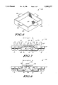
- FIG. 1 illustrates a cross-sectional view of a semiconductor device 10 in accordance with the present invention.
- Device 10 includes a circuitized substrate 12.
- Substrate 12 is called a circuitized substrate because it is used for routing electrical signals to and from a semiconductor die 13.
- substrate 12 includes a plurality of conductive traces 14 on its top surface. In most instances, conductive traces will also be on a bottom surface the substrate (although not fully illustrated in FIG. 1). Traces on the bottom of substrate 12 each terminate with a conductive pad 16.
- Conductive traces on the top and bottom of the substrate are electrically coupled together, most often in a one-to-one correspondence, by a plurality of conductive vias 18 which extend through substrate 12. It is helpful to note that since FIG.
- FIG. 1 illustrates only a cross-sectional view of substrate 12, not all traces, vias, and pads of device 10 are represented. Electrical signals are routed from the substrate to semiconductor die 13 by a plurality of conductive wires 19, or by other known coupling methods such as tape-automated-bonding (TAB), which electrically coupled the die to conductive traces 14. External electrical access to semiconductor die 13 is established through a plurality of solder balls 21, each metallurgically bonded to a conductive pad 16. Typically, pads 16 and solder balls 21 will be arranged in an array configuration on the bottom of substrate 12, thus device 10 is referred to as a pad array or ball array device.
- TAB tape-automated-bonding
- conductive pins may be coupled to pads 16 to establish a pin grid array device also in accordance with the present invention.
- pads 16 can be electrically bonded or coupled directly to an underlying substrate without use of balls or pins.
- Substrate 12 is manufactured using conventional processes.
- the bulk material used for the substrate is preferably a glass, fabric-reinforced resin, such as an epoxy, polyimide, triazine, or phenolic resin. More specifically, a bismaleimide-triazine (BT) resin is preferred; however, other substrate materials are also suitable. For instance, various epoxy-glass composites, printed circuit board (PCB) materials, flexible circuits, or ceramic substrates may be used. Also, reinforcements other than glass can be used in a substrate, such as aramid and ceramic fibers. Likewise, particle reinforcements may be used instead of fibers.
- BT bismaleimide-triazine
- reinforcements other than glass can be used in a substrate, such as aramid and ceramic fibers. Likewise, particle reinforcements may be used instead of fibers.
- Conductive traces 14 and conductive pads 16 are typically formed on substrate 14 by laminating a conductive foil or by plating a conductive film to the substrate, wherein the conductive material is usually copper. Traces and pads are defined by patterning the foil using lithography techniques. Alternatively, traces and pads may be screen printed or otherwise deposited onto surfaces of the substrate. Both the conductive traces and pads are typically plated with gold to establish a non-oxidizable surfaces suitable for bonding. Thus, the traces and pads will typically include two layers, a laminated layer of copper and an overlying plated layer of gold or a combination of nickel and gold. However, for purposes of clarity the conductive traces, pads, and vias are illustrated as being of a single layer of material throughout the description of the present invention.
- Conductive vias 18 are typically formed in substrate 12 by drilling or punching holes through the substrate and subsequently plating the holes with copper, and sometimes also with nickel and gold, so that only sidewalls of the holes are conductive.
- holes may be molded into a substrate and later plated to formed conductive vias. In either case, the resulting vias are usually hollow.
- substrate 12 includes an opening 20 which extends completely through the substrate. Opening 20 is preferably punched or routed out of the substrate material after conductive traces 14 and pads 16 have been defined, although the opening can be created at any point in manufacturing substrate 12, and the opening need not be punched. For reasons related to the shape of most conventional semiconductor die, opening 20 is preferably square or rectangular. Positioned within opening 20 is a heat sink 22. Heat sink 22 includes a base portion 24, sidewalls 26, and flanges 28. Together the base portion and sidewalls of the heat sink form a cavity for receiving semiconductor die 13. The die is mounted to base portion 24 of the heat sink by a conventional die attach material 30, such as a silver-filled epoxy. Preferably, a top surface of die 13 is approximately planar with a top surface of substrate 12 so that the overall height of device 10 is kept as small as possible. However, the top surface of die 13 could instead by raised above or recessed below the top surface of substrate 12.
- Heat sink 22 is configured so that flanges 28 rest on a top surface of substrate 12. If desired, the flanges may be adhesively attached to the substrate by an adhesive material 32 which may be either electrically conductive or non-conductive. An electrically conductive adhesive material may be useful in coupling the heat sink to ground potential if desired. For additional security, an adhesive material may also be used to bond sidewalls 26 of the heat sink to portions of the substrate exposed within opening 20. An adhesive material, however, is not required to secure the heat sink in opening 20. Heat sink 22 may be adequately secured within opening 20 by a molded package body 33 which encapsulates die 13, portions of heat sink 22 and portions of substrate 12. Also, dimensions of heat sink 22 and opening 20 may provide a tight enough fit that additional security is not necessary to hold the heat sink in place.
- Heat sink 22 is also configured so that base portion 22 is thicker than flanges 28. This thickness relationship is beneficial for several reasons. One reason is that by keeping flanges 28 thin the profile or height of device 10 can also be kept small. Another reason for making flanges 28 thin is to reduce the possibility of electrically short-circuiting conductive wires 19 to the heat sink. As illustrated in FIG. 1, in coupling die 13 to conductive traces 14, conductive wires 19 span over flanges 28 of the heat sink, creating a potential for short-circuiting. The short-circuiting probability can be reduced by making the flanges as thin as possible, by increasing the loop height of wires 19, or alternatively by using an insulating material (not shown) to cover the flanges.
- Base portion 22 is preferably quite thick so that the heat sink extends below substrate 12 to establish a continuous thermal path to a typical user substrate 34. Also, the thickness of base portion 22 establishes the planarity between the top of die 13 and the top of substrate 12.
- a thermally conductive bonding material 36 for instance solder or a thermally conductive epoxy, can be used between heat sink 22 and user substrate 34. If solder is used for bonding material 36, the heat sink can be bonded to user substrate 34 during the same solder reflow operation used to couple solder balls 21 to solder pads 35 on the user substrate.
- FIG. 2 is a cross-sectional view illustrating another semiconductor device 40 in accordance with the present invention. Since several of the elements of device 40 have already been described previously, like reference numerals are used to designate identical or corresponding elements in FIG. 2 and throughout the remaining figures of this description.
- Device 40 includes a circuitized substrate 42 which is different from the previously described circuitized substrate in that substrate 42 has a recess formed in a top surface which creates a ledge 44 surrounding opening 20.
- a heat sink 46 having a base portion 48, sidewalls 50, and flanges 52, is positioned in opening 20 such that flanges 52 rest upon ledge 44. If desired, the flanges can be secured to the ledge by adhesive material 32.
- Ledge 44 can be created in substrate 42 using known substrate manufacturing techniques. For example, the top surface of the substrate can be routed or milled to an appropriate depth either before or after opening 20 is formed. While the creation of ledge 44 adds to the manufacturing cost of substrate 42, a benefit is a lower profile device. Device 40 can be made thinner than the previously described device 10 because the flanges of the heat sink are planar with the substrate. As a result, wire bond loop heights can be reduced, as can the thickness of a package body 54, illustrated in FIG. 2 as a glob-top package body. Another benefit of making the flanges planar with substrate 42 is the reduced chance of electrically short-circuiting conductive wires 19 to heat sink 46. The depth of the ledge with respect to the top surface of substrate 42 determines the proximity of flanges 52 to conductive wires 19. Therefore, the thickness of flanges 52 is less critical than if the flanges rest on the top surface of the substrate.
- base portion 48 of heat sink 46 is configured to include fins 56. Fins 56 are provided to increase the exposed surface area of the heat sink for improved thermal conductivity.
- the exposed surface area of a portion of a heat sink used in accordance with the present invention can be increased in ways other than using fins. Generally, a surface area can be increased by creating any depressions, projections, or other topography in the surface. This type of heat sink is particularly effective in cases in which fluid is flowed under the semiconductor device for cooling purposes.
- FIG. 3 illustrates another form of the invention in which a heat sink is not inserted into an opening in a substrate, but is instead attached to the substrate such that the heat sink at least partially closes an opening in a substrate.
- a semiconductor device 60 illustrated in a cross-sectional view in FIG. 3 includes a circuitized substrate 62 having a ledge 64. Ledge 64 is formed, for example, by routing or milling a bottom surface of the substrate, as opposed to forming a ledge from a top surface of the substrate as discussed in reference to FIG. 2.
- a heat sink 66 having a base portion 68, sidewalls 70, and flanges 72, is attached to substrate 62 such that opening 20 is covered on the bottom of the substrate.
- Heat sink 66 is secured by attaching flanges 72 to ledge 64 with adhesive material 32.
- adhesive material 32 is probably necessary since substrate 62 provides no mechanical support for heat sink 66.
- ledge 64 is not necessary. Rather than using a ledge, flanges 72 can be attached directly to the bottom surface of substrate 62 while still partially covering opening 20.
- An advantage in attaching the heat sink to cover opening 20, as illustrated in FIG. 3, rather than inserting the heat sink into the opening, as illustrated in FIGS. 1 and 2, is that the potential for electrically short-circuiting conductive wires 19 to the heat sink is virtually eliminated.
- wires 19 are separated from flanges of the heat sink by ledge 64. Since the bulk material of substrate 62 is an insulator, deformation of wires 19 in a vertical direction such that the wires contact the bulk material of substrate 62 will not cause short-circuiting.
- FIGS. 4-6 illustrate in perspective views heats sinks 80, 90, and 100, respectively.
- Common features of each heat sink include a base portion, sidewalls, and flanges.
- heat sinks 80, 90, and 100 have base portions 82, 92, and 102, respectively, sidewalls 84, 94, and 104, respectively, and flanges 86, 96, and 106, respectively.
- sidewalls of a heat sink need not be contiguous with one another, nor do flanges have to extend entirely along a sidewall. Furthermore, edges of heat sinks which join the flanges, sidewalls, and base portions may be sharp or include a degree of curvature.
- Heat sinks used in accordance with the present invention may be manufactured using known techniques, including stamping, coining, etching, welding, and combinations of these techniques.
- the heat sink is made of copper, a copper alloy or other material having a high thermal conductivity. Since one advantage of present invention is that a semiconductor device can have good thermal dissipation while maintaining a low profile, it is also preferred that heat sinks used in accordance with the invention be made from a relatively thin material. However, as noted earlier, not all portions of a heat sink need be the same thickness.
- One suitable material is copper foil which is similar to, but slightly thicker than, that used to form conductive traces and pads on a circuitized substrate.
- a circuitized substrate is approximately 10 to 20 mils (0.25 to 0.51 mm) thick and solder balls each have a diameter of 25 mils (0.64 mm). Accordingly, a heat sink in accordance with the present invention preferably has a general material thickness of between 2 and 20 mils (0.05 to 0.50 mm).
- a heat sink used in a semiconductor device in accordance with the present invention can vary a great deal. Many dimensions will be dictated by the size of a semiconductor die mounted in the heat sink and the dimensions of a circuitized substrate to which the heat sink is attached. For instance, the area of a base portion of a heat sink should be slightly larger than the area of the semiconductor die and should be approximately equal to the area of an opening in the circuitized substrate. Also, the sidewalls of a heat sink should have a height at least as great as the thickness of the substrate. Dimensions and configurations of heat sink flanges are less restricted. Flanges of a heat sink may be wide enough to barely rest on a substrate or may span close to the entire distance between an opening in the substrate and any surrounding conductive traces.
- the thickness of a base portion of a heat sink is more or less unrestricted.
- the base portion thickness should be such that the top surface or active surface of the semiconductor die is planar with the circuitized substrate to achieve the smallest possible device profile.
- the die can also be made planar with the substrate by adjusting the height of the sidewalls of the heat sink.
- the base portion also preferably extends below circuitized substrate to facilitate thermal coupling to a user's substrate. However, many benefits of the present invention are achieved if the base portion is planar with the circuitized substrate.
- FIG. 7 is a cross-sectional view illustrating a semiconductor device 110.
- Device 110 and a semiconductor device 130 illustrated in FIG. 8 include many of the same elements previously described and illustrated; therefore, the same reference numerals are used to designate identical or corresponding elements.
- a circuitized substrate 112 includes opening 20 surrounded by a ledge 114. Ledge 114 is formed in a bottom surface of the substrate.
- a heat sink 116 having a base portion 118, sidewalls 120, and flanges 122. As in FIG.
- heat sink 116 is attached to the substrate in an inverted manner such that base portion 118 is exposed on a top surface of substrate 112. With the base portion exposed on the top of the substrate, a second, larger heat sink 124 can be thermally coupled to the device for added heat dissipation.
- Heat sink 124 is attached to heat sink 116 by thermally conductive bonding material 36, such as solder or a thermally conductive epoxy. If desired, heat sink 124 can have a topography or contoured surface to maximize the exposed surface area by the inclusion of, for example, fins 126.
- heat sink 116 With heat sink 116 inverted, semiconductor die 13 is face-down as illustrated in FIG. 7. Therefore, electrical interconnection between the die and circuitized substrate 112 is accomplished on the bottom surface of the substrate by conductive traces 14, conductive pads 16, and conductive wires 19. Likewise, package body 33 is formed on the bottom surface of the substrate amidst solder balls 21. The presence of package body on the bottom surface of substrate 112 somewhat restricts the location of solder balls 21 and may increase the footprint of the device; however, in some instances the added heat dissipation capabilities of a second heat sink are needed.
- FIG. 8 A similar inverted semiconductor device 130 is illustrated in a cross-sectional view in FIG. 8.
- Device 130 includes a circuitized substrate 132 in which opening 20 is surrounded by a ledge 134.
- the ledge is formed in a top surface of substrate 132.
- a heat sink 136 having a base portion 138, sidewalls 140, and flanges 142.
- ledge 134 is not necessary.
- flanges 142 can be attached directly to the top surface of substrate 132 while still covering opening 20.
- the heat sink of device 130 is not inserted into opening 20 but instead is attached to substrate 132 so that the opening is at least partially closed, specifically so that the top of the opening is covered.
- device 130 is similar to the device illustrated in FIG. 3 but is inverted so that most or all circuitry and electrically interconnections are on the bottom of substrate 132.
- An advantage of including circuitry only on the bottom of substrate 132 is a lower substrate cost, due to the fact that conductive vias are not required and only one layer of metallization is used.
- FIG. 8 also demonstrates that encapsulation of a semiconductor die need not be accomplished with a molded or resin package body.
- Device 130 includes a lid 144 which encapsulates semiconductor die 13, conductive wires 19, and portions of conductive traces 14. Together, lid 144 and heat sink 136 fully enclose opening 20 of the substrate.
- Lid 144 can be made from a conventional semiconductor packaging material, including metals, plastics, and ceramics.
- the configuration of a heat sink used in accordance with the present invention enables the heat sink to be incorporated as part of a conventional substrate rather than an external component of a semiconductor device.
- the size of a device in accordance with the present invention is comparable to conventional pad array devices yet has improved thermal dissipation.
- the improvement in thermal dissipation is achieved because the entire base portion of the heat sink serves as the thermal dissipation area, as opposed to the cross-sectional area of thermal vias used in conventional devices.
- a direct thermal path to a user substrate can be easily established by extending a base portion of the heat sink below a circuitized substrate.
- the die receiving cavity of the heat sink results in a reduced device height or profile since a semiconductor die is mounted below the surface of the substrate.
- a heat sink of a device acts as an excellent barrier to moisture ingress into the area near the semiconductor die.
- a further advantage of the present invention is the many ways in which the heat sink can be attached to a circuitized substrate.
- the heat sink can be inserted in an opening of the substrate such that the flanges rest on a surface of the substrate and secure the heat sink in position.
- flanges of the heat sink may be attached to a surface of the substrate such that the heat sink encloses one side of the opening in the substrate, rather than being inserted into the opening.
- the heat sink can be attached to either a top or a bottom surface of the substrate.
- recesses may be formed in a substrate surface such that flanges of the heat sink rest on the ledges.
- the heat sink may be attached to substrate in an inverted manner resulting in a "die-down" device configuration.
- a heat sink used in a device in accordance with the present invention need not have the specific configurations illustrated herein and need not have the dimensional relationships described.
- a base portion and/or sidewalls of a heat sink need not extend below a bottom surface of the substrate.
- the invention is not limited to those specific materials described.
- encapsulation of a semiconductor device may include any known encapsulation method such as resin molding compounds, glob-top resins, metal lids, ceramic lids, and the like.
- a semiconductor die can be coupled to a circuitized substrate materials using any known coupling methods.
- any existing circuitized substrate can be used in accordance with the present invention. It is also important to note that the present invention is applicable to multichip module devices in addition to embodiments having a single semiconductor die.
- a heat sink used in accordance with the present invention to serve as a voltage reference plane, for instance a ground potential plane, in addition to providing thermal dissipation. Using the heat sink as a voltage plane can easily be achieved by electrically coupling the heat sink to one or more appropriate conductive traces of the circuitized substrate. Therefore, it is intended that this invention encompass all such variations and modifications as fall within the scope of the appended claims.
Abstract
Description
Claims (13)
Priority Applications (1)
| Application Number | Priority Date | Filing Date | Title |
|---|---|---|---|
| US08/537,169 US5583377A (en) | 1992-07-15 | 1995-09-29 | Pad array semiconductor device having a heat sink with die receiving cavity |
Applications Claiming Priority (2)
| Application Number | Priority Date | Filing Date | Title |
|---|---|---|---|
| US91331992A | 1992-07-15 | 1992-07-15 | |
| US08/537,169 US5583377A (en) | 1992-07-15 | 1995-09-29 | Pad array semiconductor device having a heat sink with die receiving cavity |
Related Parent Applications (1)
| Application Number | Title | Priority Date | Filing Date |
|---|---|---|---|
| US91331992A Continuation | 1992-07-15 | 1992-07-15 |
Publications (1)
| Publication Number | Publication Date |
|---|---|
| US5583377A true US5583377A (en) | 1996-12-10 |
Family
ID=25433161
Family Applications (1)
| Application Number | Title | Priority Date | Filing Date |
|---|---|---|---|
| US08/537,169 Expired - Lifetime US5583377A (en) | 1992-07-15 | 1995-09-29 | Pad array semiconductor device having a heat sink with die receiving cavity |
Country Status (1)
| Country | Link |
|---|---|
| US (1) | US5583377A (en) |
Cited By (128)
| Publication number | Priority date | Publication date | Assignee | Title |
|---|---|---|---|---|
| WO1997030477A1 (en) * | 1996-02-14 | 1997-08-21 | Olin Corporation | Ball grid array electronic package standoff design |
| US5717252A (en) * | 1994-07-25 | 1998-02-10 | Mitsui High-Tec, Inc. | Solder-ball connected semiconductor device with a recessed chip mounting area |
| US5798909A (en) * | 1995-02-15 | 1998-08-25 | International Business Machines Corporation | Single-tiered organic chip carriers for wire bond-type chips |
| US5831825A (en) * | 1995-06-13 | 1998-11-03 | Bull, S.A. | Integrated circuit IC package and a process for cooling an integrated circuit mounted in an IC package |
| US5831826A (en) * | 1996-09-20 | 1998-11-03 | Motorola, Inc. | Heat transfer apparatus suitable for use in a circuit board assembly |
| US5851337A (en) * | 1997-06-30 | 1998-12-22 | Caesar Technology Inc. | Method of connecting TEHS on PBGA and modified connecting structure |
| US5852324A (en) * | 1996-01-25 | 1998-12-22 | Sgs-Thomson Microelectronics S.R.L. | Plastic body surface-mounting semiconductor power device having dimensional characteristics optimized for use of standard shipping and testing modes |
| US5856911A (en) * | 1996-11-12 | 1999-01-05 | National Semiconductor Corporation | Attachment assembly for integrated circuits |
| US5886409A (en) * | 1996-01-16 | 1999-03-23 | Hitachi, Ltd. | Electrode structure of wiring substrate of semiconductor device having expanded pitch |
| US5901042A (en) * | 1997-04-21 | 1999-05-04 | Matsushita Electric Industrial Co., Ltd. | Package and semiconductor device |
| US5903052A (en) * | 1998-05-12 | 1999-05-11 | Industrial Technology Research Institute | Structure for semiconductor package for improving the efficiency of spreading heat |
| US5995371A (en) * | 1996-09-19 | 1999-11-30 | Murata Manufacturing Co., Ltd. | Integrated dielectric substrate |
| US6028355A (en) * | 1998-06-16 | 2000-02-22 | At&T Corp. | Method and apparatus for dissipating heat from an enclosed printed wiring board |
| US6060777A (en) * | 1998-07-21 | 2000-05-09 | Intel Corporation | Underside heat slug for ball grid array packages |
| EP1003214A2 (en) * | 1998-11-17 | 2000-05-24 | Fujitsu Limited | Semiconductor device and method of producing the same |
| USRE36773E (en) * | 1993-10-18 | 2000-07-11 | Motorola, Inc. | Method for plating using nested plating buses and semiconductor device having the same |
| US6163069A (en) * | 1997-10-09 | 2000-12-19 | Mitsubishi Denki Kabushiki Kaisha | Semiconductor device having pads for connecting a semiconducting element to a mother board |
| US6191360B1 (en) * | 1999-04-26 | 2001-02-20 | Advanced Semiconductor Engineering, Inc. | Thermally enhanced BGA package |
| US6219254B1 (en) * | 1999-04-05 | 2001-04-17 | Trw Inc. | Chip-to-board connection assembly and method therefor |
| US6225686B1 (en) * | 1996-11-21 | 2001-05-01 | Sony Corporation | Semiconductor device |
| US6271581B2 (en) * | 1999-11-08 | 2001-08-07 | Siliconware Precision Industries Co., Ltd. | Semiconductor package structure having universal lead frame and heat sink |
| US6282094B1 (en) | 1999-04-12 | 2001-08-28 | Siliconware Precision Industries, Co., Ltd. | Ball-grid array integrated circuit package with an embedded type of heat-dissipation structure and method of manufacturing the same |
| US6291892B1 (en) * | 1998-04-02 | 2001-09-18 | Oki Electric Industry Co., Ltd | Semiconductor package that includes a shallow metal basin surrounded by an insulator frame |
| US6297550B1 (en) | 1998-04-01 | 2001-10-02 | Lsi Logic Corporation | Bondable anodized aluminum heatspreader for semiconductor packages |
| US6339253B1 (en) * | 1999-08-30 | 2002-01-15 | Micron Technology, Inc. | Semiconductor package |
| US6353182B1 (en) * | 1997-08-18 | 2002-03-05 | International Business Machines Corporation | Proper choice of the encapsulant volumetric CTE for different PGBA substrates |
| US6362964B1 (en) * | 1999-11-17 | 2002-03-26 | International Rectifier Corp. | Flexible power assembly |
| US20020041021A1 (en) * | 2000-10-05 | 2002-04-11 | Noriaki Sakamoto | Semiconductor device, semiconductor module and hard disk |
| US6404048B2 (en) * | 1998-09-03 | 2002-06-11 | Micron Technology, Inc. | Heat dissipating microelectronic package |
| WO2002050899A2 (en) * | 2000-12-19 | 2002-06-27 | Convergence Technologies, Ltd. | Semiconductor package |
| US6424026B1 (en) * | 1999-08-02 | 2002-07-23 | International Rectifier Corporation | Power module with closely spaced printed circuit board and substrate |
| US6429512B1 (en) * | 1999-03-16 | 2002-08-06 | Siliconware Precision Industries Co., Ltd. | Ball grid array integrated circuit package with palladium coated heat-dissipation device |
| US20020135065A1 (en) * | 2000-12-01 | 2002-09-26 | Zhao Sam Ziqun | Thermally and electrically enhanced ball grid array packaging |
| US6490173B2 (en) | 2000-12-19 | 2002-12-03 | Thomson Licensing, S.A. | Method and apparatus for providing electromagnetic shielding |
| US20020189853A1 (en) * | 2001-06-15 | 2002-12-19 | Phoenix Precision Technology Corp. | BGA substrate with direct heat dissipating structure |
| WO2002103788A1 (en) * | 2001-06-18 | 2002-12-27 | International Rectifier Corporation | High voltage semiconductor device housing with increased clearance between housing can and die for improved flux flushing |
| KR100352119B1 (en) * | 1996-12-13 | 2002-12-31 | 앰코 테크놀로지 코리아 주식회사 | Structure of ball grid array semiconductor package having heatsink and fabricating method thereof |
| US20030034553A1 (en) * | 2001-08-15 | 2003-02-20 | Kazuaki Ano | Low profile ball-grid array package for high power |
| US6532157B1 (en) * | 2000-11-16 | 2003-03-11 | Amkor Technology, Inc. | Angulated semiconductor packages |
| US6537848B2 (en) | 2001-05-30 | 2003-03-25 | St. Assembly Test Services Ltd. | Super thin/super thermal ball grid array package |
| US20030057550A1 (en) * | 2000-12-22 | 2003-03-27 | Broadcom Corporation | Ball grid array package enhanced with a thermal and electrical connector |
| US20030077853A1 (en) * | 1997-07-02 | 2003-04-24 | Kinsman Larry D. | Varied-thickness heat sink for integrated circuit (IC) packages and method of fabricating IC packages |
| US6555900B1 (en) * | 1998-10-21 | 2003-04-29 | Matsushita Electric Industrial Co., Ltd. | Package, semiconductor device and method for fabricating the semiconductor device |
| US6559536B1 (en) * | 1999-12-13 | 2003-05-06 | Fujitsu Limited | Semiconductor device having a heat spreading plate |
| US6565267B2 (en) | 2001-05-08 | 2003-05-20 | Fujitsu Limited | Optical transmitting device and optical receiving device each having receptacle type optical module |
| US20030098514A1 (en) * | 1999-11-23 | 2003-05-29 | Bolken Todd O. | Packages for semiconductor die |
| US6576988B2 (en) | 1999-08-30 | 2003-06-10 | Micron Technology, Inc. | Semiconductor package |
| US20030111726A1 (en) * | 2001-12-18 | 2003-06-19 | Khan Reza-Ur Rahman | Ball grid array package substrates and method of making the same |
| EP1333490A2 (en) | 2002-02-01 | 2003-08-06 | Broadcom Corporation | Ball grid array package with patterned stiffener layer |
| US20030146506A1 (en) * | 2002-02-01 | 2003-08-07 | Broadcom Corporation | Ball grid array package fabrication with IC die support structures |
| US20030146511A1 (en) * | 2002-02-01 | 2003-08-07 | Broadcom Corporation | Ball grid array package with multiple interposers |
| US20030146503A1 (en) * | 2002-02-01 | 2003-08-07 | Broadcom Corporation | Ball grid array package with stepped stiffener layer |
| US20030178719A1 (en) * | 2002-03-22 | 2003-09-25 | Combs Edward G. | Enhanced thermal dissipation integrated circuit package and method of manufacturing enhanced thermal dissipation integrated circuit package |
| US20030179556A1 (en) * | 2002-03-21 | 2003-09-25 | Broadcom Corporation | Enhanced die-up ball grid array package with two substrates and method for making the same |
| US20040042178A1 (en) * | 2002-09-03 | 2004-03-04 | Vadim Gektin | Heat spreader with surface cavity |
| US6747344B2 (en) * | 1997-07-02 | 2004-06-08 | Micron Technology, Inc. | Lead frame assemblies with voltage reference plane and IC packages including same |
| US20040150083A1 (en) * | 2000-05-10 | 2004-08-05 | Samsung Electronic Co., Ltd. | Method for manufacturing digital micro-mirror device (DMD) |
| US6790710B2 (en) | 2002-01-31 | 2004-09-14 | Asat Limited | Method of manufacturing an integrated circuit package |
| US6853070B2 (en) | 2001-02-15 | 2005-02-08 | Broadcom Corporation | Die-down ball grid array package with die-attached heat spreader and method for making the same |
| US20050046039A1 (en) * | 2003-08-27 | 2005-03-03 | Advanced Semiconductor Engineering, Inc. | Flip-chip package |
| US6900535B2 (en) * | 2002-05-01 | 2005-05-31 | Stmicroelectronics, Inc. | BGA/LGA with built in heat slug/spreader |
| US20050121759A1 (en) * | 2003-10-21 | 2005-06-09 | Stmicroelectronics S.A. | Semiconductor package with a chip on a support plate |
| US20050275086A1 (en) * | 2004-06-09 | 2005-12-15 | Lsi Logic Corporation | Semiconductor package and process utilizing pre-formed mold cap and heatspreader assembly |
| US20060012019A1 (en) * | 2004-07-14 | 2006-01-19 | Samsung Electronics Co., Ltd. | Semiconductor package |
| US6989593B2 (en) | 2000-12-22 | 2006-01-24 | Broadcom Corporation | Die-up ball grid array package with patterned stiffener opening |
| US20060081980A1 (en) * | 2003-05-28 | 2006-04-20 | Infineon Technologies Ag | Integrated circuit package employing a heat-spreader member |
| US20060087009A1 (en) * | 2004-10-21 | 2006-04-27 | Ching-Hsu Yang | Cavity-down multiple-chip package |
| US20060103010A1 (en) * | 2004-11-12 | 2006-05-18 | Stats Chippac Ltd. | Semiconductor package system with substrate heat sink |
| US20060139089A1 (en) * | 2004-12-29 | 2006-06-29 | Bambridge Timothy B | Intelligent high-power amplifier module |
| US20060139896A1 (en) * | 2004-12-29 | 2006-06-29 | Bambridge Timothy B | Packaging for electronic modules |
| US20060170092A1 (en) * | 2005-02-01 | 2006-08-03 | Stats Chippac Ltd. | Semiconductor package system with cavity substrate |
| US20060186536A1 (en) * | 2005-02-02 | 2006-08-24 | Shih-Ping Hsu | Substrate assembly with direct electrical connection as a semiconductor package |
| US20060220222A1 (en) * | 2005-03-29 | 2006-10-05 | Zhao-Chong Zeng | Chip embedded package structure and fabrication method thereof |
| US7132744B2 (en) * | 2000-12-22 | 2006-11-07 | Broadcom Corporation | Enhanced die-up ball grid array packages and method for making the same |
| US7196415B2 (en) | 2002-03-22 | 2007-03-27 | Broadcom Corporation | Low voltage drop and high thermal performance ball grid array package |
| US20070090522A1 (en) * | 2005-09-26 | 2007-04-26 | Iyad Alhayek | Integrated circuit mounting for thermal stress relief useable in a multi-chip module |
| US20070184644A1 (en) * | 2003-06-30 | 2007-08-09 | Intel Corporation | Ball grid array copper balancing |
| US7259457B2 (en) | 2001-05-07 | 2007-08-21 | Broadcom Corporation | Die-up ball grid array package including a substrate capable of mounting an integrated circuit die and method for making the same |
| US20070238205A1 (en) * | 2006-04-06 | 2007-10-11 | Robert Bauer | Lead frame based, over-molded semiconductor package with integrated through hole technology (THT) heat spreader pin(s) and associated method of manufacturing |
| US20070291457A1 (en) * | 2006-06-16 | 2007-12-20 | Huili Fu | IC packages with internal heat dissipation structures |
| US20080032456A1 (en) * | 2006-08-03 | 2008-02-07 | Stats Chippac Ltd. | Integrated circuit package system with down-set die pad |
| US7399657B2 (en) * | 2000-08-31 | 2008-07-15 | Micron Technology, Inc. | Ball grid array packages with thermally conductive containers |
| DE102007002156A1 (en) * | 2007-01-15 | 2008-07-17 | Infineon Technologies Ag | Semiconductor arrangement, comprises heat sink body, which is provided for dissipating heat from semiconductor component, where heat sink has electric conductive body with recess for receiving semiconductor component |
| US7411281B2 (en) | 2004-06-21 | 2008-08-12 | Broadcom Corporation | Integrated circuit device package having both wire bond and flip-chip interconnections and method of making the same |
| US20080211087A1 (en) * | 2006-12-20 | 2008-09-04 | Infineon Technologies Ag | Chip module and method for producing a chip module |
| US7432586B2 (en) | 2004-06-21 | 2008-10-07 | Broadcom Corporation | Apparatus and method for thermal and electromagnetic interference (EMI) shielding enhancement in die-up array packages |
| US7439099B1 (en) * | 2002-12-02 | 2008-10-21 | Asat Ltd. | Thin ball grid array package |
| US7482686B2 (en) | 2004-06-21 | 2009-01-27 | Braodcom Corporation | Multipiece apparatus for thermal and electromagnetic interference (EMI) shielding enhancement in die-up array packages and method of making the same |
| US7550845B2 (en) | 2002-02-01 | 2009-06-23 | Broadcom Corporation | Ball grid array package with separated stiffener layer |
| US20090294947A1 (en) * | 2008-05-29 | 2009-12-03 | Industrial Technology Research Institute | Chip package structure and manufacturing method thereof |
| US20090309213A1 (en) * | 2008-06-12 | 2009-12-17 | Renesas Technology Corp. | Semiconductor device and manufacturing method of the same |
| US7754976B2 (en) * | 2002-04-15 | 2010-07-13 | Hamilton Sundstrand Corporation | Compact circuit carrier package |
| US7786591B2 (en) | 2004-09-29 | 2010-08-31 | Broadcom Corporation | Die down ball grid array package |
| US20100265665A1 (en) * | 2009-04-15 | 2010-10-21 | Yukihiro Kozaka | Electronic device having a heat sink |
| US20110039374A1 (en) * | 2008-03-25 | 2011-02-17 | Bridge Semiconductor Corporation | Method of making a semiconductor chip assembly with a bump/base heat spreader and a cavity in the bump |
| US20110065241A1 (en) * | 2008-03-25 | 2011-03-17 | Bridge Semiconductor Corporation | Method of making a semiconductor chip assembly with a bump/base heat spreader and a dual-angle cavity in the bump |
| US20110133329A1 (en) * | 2009-12-08 | 2011-06-09 | Renesas Electronics Corporation | Semiconductor device and method of manufacturing the same |
| US20110227122A1 (en) * | 2008-03-25 | 2011-09-22 | Bridge Semiconductor Corporation | Semiconductor chip assembly with post/base heat spreader with thermal via |
| US8183680B2 (en) | 2006-05-16 | 2012-05-22 | Broadcom Corporation | No-lead IC packages having integrated heat spreader for electromagnetic interference (EMI) shielding and thermal enhancement |
| US20120129299A1 (en) * | 2010-11-22 | 2012-05-24 | Bridge Semiconductor Corporation | Method of making thermally enhanced semiconductor assembly with bump/base/flange heat spreader and build-up circuitry |
| US20120126401A1 (en) * | 2010-11-22 | 2012-05-24 | Bridge Semiconductor Corporation | Stackable semiconductor assembly with bump/base/flange heat spreader and electromagnetic shielding |
| CN102738022A (en) * | 2011-04-15 | 2012-10-17 | 飞思卡尔半导体公司 | Method for assembling semiconductor device containing insulating substrate and heat sink |
| US8362609B1 (en) | 2009-10-27 | 2013-01-29 | Xilinx, Inc. | Integrated circuit package and method of forming an integrated circuit package |
| US20130087927A1 (en) * | 2007-10-22 | 2013-04-11 | Nec Corporation | Multimedia providing service |
| JP2013084675A (en) * | 2011-10-06 | 2013-05-09 | Shindengen Electric Mfg Co Ltd | Electric connection structure of semiconductor element |
| US8556159B2 (en) | 2012-02-24 | 2013-10-15 | Freescale Semiconductor, Inc. | Embedded electronic component |
| US20130308278A1 (en) * | 2012-05-21 | 2013-11-21 | International Business Machines Corporation | Achieving power supply and heat dissipation (cooling) in three-dimensional multilayer package |
| EP2687350A1 (en) * | 2011-03-17 | 2014-01-22 | Iriso Electronics Co., Ltd. | Resin molded product and method for producing same |
| US20140085845A1 (en) * | 2012-09-27 | 2014-03-27 | Hon Hai Precision Industry Co., Ltd. | Thick-film hybrid circuit structure and method of manufacture the same |
| US8766453B2 (en) | 2012-10-25 | 2014-07-01 | Freescale Semiconductor, Inc. | Packaged integrated circuit having large solder pads and method for forming |
| US8810028B1 (en) | 2010-06-30 | 2014-08-19 | Xilinx, Inc. | Integrated circuit packaging devices and methods |
| US20150214127A1 (en) * | 2014-01-24 | 2015-07-30 | Qualcomm Incorporated | Integrated device comprising a substrate with aligning trench and/or cooling cavity |
| US20150371934A1 (en) * | 2014-06-19 | 2015-12-24 | J-Devices Corporation | Semiconductor package and method of manufacturing the same |
| US20160343755A1 (en) * | 2015-05-19 | 2016-11-24 | Renesas Electronics Corporation | Semiconductor device |
| EP3121849A3 (en) * | 2015-07-22 | 2017-02-01 | Nxp B.V. | Heatsink very-thin quad flat no-leads (hvqfn) package |
| WO2017052852A1 (en) * | 2015-09-24 | 2017-03-30 | Intel Corporation | Package topside ball grid array for ultra low z-height |
| US20170162479A1 (en) * | 2015-12-03 | 2017-06-08 | Stmicroelectronics, Inc. | Semiconductor device with frame having arms and related methods |
| US9780014B1 (en) | 2011-11-29 | 2017-10-03 | Hrl Laboratories, Llc | Simultaneous controlled depth hot embossing and active side protection during packaging and assembly of wide bandgap devices |
| US9837372B1 (en) * | 2015-05-22 | 2017-12-05 | Hrl Laboratories, Llc | Wafer-level die to package and die to die interconnects suspended over integrated heat sinks |
| US10026672B1 (en) * | 2015-10-21 | 2018-07-17 | Hrl Laboratories, Llc | Recursive metal embedded chip assembly |
| US10079160B1 (en) * | 2013-06-21 | 2018-09-18 | Hrl Laboratories, Llc | Surface mount package for semiconductor devices with embedded heat spreaders |
| US10134711B2 (en) | 2015-05-27 | 2018-11-20 | Bridge Semiconductor Corporation | Thermally enhanced semiconductor assembly with three dimensional integration and method of making the same |
| US10269678B1 (en) * | 2017-12-05 | 2019-04-23 | Nxp Usa, Inc. | Microelectronic components having integrated heat dissipation posts, systems including the same, and methods for the fabrication thereof |
| US20190206762A1 (en) * | 2014-02-25 | 2019-07-04 | International Business Machines Corporation | Tim strain mitigation in electronic modules |
| US10923786B2 (en) | 2018-08-31 | 2021-02-16 | Dana Automotive Systems Group, Llc | Housing assembly for one or more electro chemical cells |
| US10950562B1 (en) | 2018-11-30 | 2021-03-16 | Hrl Laboratories, Llc | Impedance-matched through-wafer transition using integrated heat-spreader technology |
| US11291146B2 (en) | 2014-03-07 | 2022-03-29 | Bridge Semiconductor Corp. | Leadframe substrate having modulator and crack inhibiting structure and flip chip assembly using the same |
| US11462476B2 (en) * | 2018-01-31 | 2022-10-04 | Tdk Electronics Ag | Electronic device |
Citations (7)
| Publication number | Priority date | Publication date | Assignee | Title |
|---|---|---|---|---|
| US3399332A (en) * | 1965-12-29 | 1968-08-27 | Texas Instruments Inc | Heat-dissipating support for semiconductor device |
| US4737395A (en) * | 1983-11-29 | 1988-04-12 | Ibiden Co. Ltd. | Printed wiring board for mounting electronic parts and process for producing the same |
| US4829403A (en) * | 1987-01-20 | 1989-05-09 | Harding Ade Yemi S K | Packaging arrangement for energy dissipating devices |
| US4835598A (en) * | 1985-06-13 | 1989-05-30 | Matsushita Electric Works, Ltd. | Wiring board |
| US4890152A (en) * | 1986-02-14 | 1989-12-26 | Matsushita Electric Works, Ltd. | Plastic molded chip carrier package and method of fabricating the same |
| US5045921A (en) * | 1989-12-26 | 1991-09-03 | Motorola, Inc. | Pad array carrier IC device using flexible tape |
| US5233225A (en) * | 1988-02-05 | 1993-08-03 | Citizen Watch Co., Ltd. | Resin encapsulated pin grid array and method of manufacturing the same |
-
1995
- 1995-09-29 US US08/537,169 patent/US5583377A/en not_active Expired - Lifetime
Patent Citations (7)
| Publication number | Priority date | Publication date | Assignee | Title |
|---|---|---|---|---|
| US3399332A (en) * | 1965-12-29 | 1968-08-27 | Texas Instruments Inc | Heat-dissipating support for semiconductor device |
| US4737395A (en) * | 1983-11-29 | 1988-04-12 | Ibiden Co. Ltd. | Printed wiring board for mounting electronic parts and process for producing the same |
| US4835598A (en) * | 1985-06-13 | 1989-05-30 | Matsushita Electric Works, Ltd. | Wiring board |
| US4890152A (en) * | 1986-02-14 | 1989-12-26 | Matsushita Electric Works, Ltd. | Plastic molded chip carrier package and method of fabricating the same |
| US4829403A (en) * | 1987-01-20 | 1989-05-09 | Harding Ade Yemi S K | Packaging arrangement for energy dissipating devices |
| US5233225A (en) * | 1988-02-05 | 1993-08-03 | Citizen Watch Co., Ltd. | Resin encapsulated pin grid array and method of manufacturing the same |
| US5045921A (en) * | 1989-12-26 | 1991-09-03 | Motorola, Inc. | Pad array carrier IC device using flexible tape |
Cited By (245)
| Publication number | Priority date | Publication date | Assignee | Title |
|---|---|---|---|---|
| USRE36773E (en) * | 1993-10-18 | 2000-07-11 | Motorola, Inc. | Method for plating using nested plating buses and semiconductor device having the same |
| US5717252A (en) * | 1994-07-25 | 1998-02-10 | Mitsui High-Tec, Inc. | Solder-ball connected semiconductor device with a recessed chip mounting area |
| US5798909A (en) * | 1995-02-15 | 1998-08-25 | International Business Machines Corporation | Single-tiered organic chip carriers for wire bond-type chips |
| US5831825A (en) * | 1995-06-13 | 1998-11-03 | Bull, S.A. | Integrated circuit IC package and a process for cooling an integrated circuit mounted in an IC package |
| US5886409A (en) * | 1996-01-16 | 1999-03-23 | Hitachi, Ltd. | Electrode structure of wiring substrate of semiconductor device having expanded pitch |
| US6137185A (en) * | 1996-01-16 | 2000-10-24 | Hitachi, Ltd. | Electrode structure of a wiring substrate of semiconductor device having expanded pitch |
| US5852324A (en) * | 1996-01-25 | 1998-12-22 | Sgs-Thomson Microelectronics S.R.L. | Plastic body surface-mounting semiconductor power device having dimensional characteristics optimized for use of standard shipping and testing modes |
| US5805427A (en) * | 1996-02-14 | 1998-09-08 | Olin Corporation | Ball grid array electronic package standoff design |
| WO1997030477A1 (en) * | 1996-02-14 | 1997-08-21 | Olin Corporation | Ball grid array electronic package standoff design |
| US5995371A (en) * | 1996-09-19 | 1999-11-30 | Murata Manufacturing Co., Ltd. | Integrated dielectric substrate |
| US5831826A (en) * | 1996-09-20 | 1998-11-03 | Motorola, Inc. | Heat transfer apparatus suitable for use in a circuit board assembly |
| US5856911A (en) * | 1996-11-12 | 1999-01-05 | National Semiconductor Corporation | Attachment assembly for integrated circuits |
| US6225686B1 (en) * | 1996-11-21 | 2001-05-01 | Sony Corporation | Semiconductor device |
| KR100352119B1 (en) * | 1996-12-13 | 2002-12-31 | 앰코 테크놀로지 코리아 주식회사 | Structure of ball grid array semiconductor package having heatsink and fabricating method thereof |
| US5901042A (en) * | 1997-04-21 | 1999-05-04 | Matsushita Electric Industrial Co., Ltd. | Package and semiconductor device |
| US5851337A (en) * | 1997-06-30 | 1998-12-22 | Caesar Technology Inc. | Method of connecting TEHS on PBGA and modified connecting structure |
| US7125749B2 (en) | 1997-07-02 | 2006-10-24 | Micron Technology, Inc. | Varied-thickness heat sink for integrated circuit (IC) packages and method of fabricating IC packages |
| US6747344B2 (en) * | 1997-07-02 | 2004-06-08 | Micron Technology, Inc. | Lead frame assemblies with voltage reference plane and IC packages including same |
| US20030077853A1 (en) * | 1997-07-02 | 2003-04-24 | Kinsman Larry D. | Varied-thickness heat sink for integrated circuit (IC) packages and method of fabricating IC packages |
| US6353182B1 (en) * | 1997-08-18 | 2002-03-05 | International Business Machines Corporation | Proper choice of the encapsulant volumetric CTE for different PGBA substrates |
| US6163069A (en) * | 1997-10-09 | 2000-12-19 | Mitsubishi Denki Kabushiki Kaisha | Semiconductor device having pads for connecting a semiconducting element to a mother board |
| US6297550B1 (en) | 1998-04-01 | 2001-10-02 | Lsi Logic Corporation | Bondable anodized aluminum heatspreader for semiconductor packages |
| US20050042803A1 (en) * | 1998-04-02 | 2005-02-24 | Tadashi Yamaguchi | Semiconductor device and method for production thereof |
| US6867066B2 (en) | 1998-04-02 | 2005-03-15 | Oki Electric Industry Co., Ltd. | Method for production of a semiconductor device with package that includes an insulator frame on a metal member |
| US6977190B2 (en) | 1998-04-02 | 2005-12-20 | Oki Electric Industry Co., Ltd. | Semiconductor device and method for production thereof |
| US6291892B1 (en) * | 1998-04-02 | 2001-09-18 | Oki Electric Industry Co., Ltd | Semiconductor package that includes a shallow metal basin surrounded by an insulator frame |
| US5903052A (en) * | 1998-05-12 | 1999-05-11 | Industrial Technology Research Institute | Structure for semiconductor package for improving the efficiency of spreading heat |
| US6028355A (en) * | 1998-06-16 | 2000-02-22 | At&T Corp. | Method and apparatus for dissipating heat from an enclosed printed wiring board |
| US6060777A (en) * | 1998-07-21 | 2000-05-09 | Intel Corporation | Underside heat slug for ball grid array packages |
| US6545351B1 (en) | 1998-07-21 | 2003-04-08 | Intel Corporation | Underside heat slug for ball grid array packages |
| US6404048B2 (en) * | 1998-09-03 | 2002-06-11 | Micron Technology, Inc. | Heat dissipating microelectronic package |
| US6555900B1 (en) * | 1998-10-21 | 2003-04-29 | Matsushita Electric Industrial Co., Ltd. | Package, semiconductor device and method for fabricating the semiconductor device |
| EP1003214A2 (en) * | 1998-11-17 | 2000-05-24 | Fujitsu Limited | Semiconductor device and method of producing the same |
| EP1003214A3 (en) * | 1998-11-17 | 2002-09-11 | Fujitsu Limited | Semiconductor device and method of producing the same |
| US6288444B1 (en) * | 1998-11-17 | 2001-09-11 | Fujitsu Limited | Semiconductor device and method of producing the same |
| US6429512B1 (en) * | 1999-03-16 | 2002-08-06 | Siliconware Precision Industries Co., Ltd. | Ball grid array integrated circuit package with palladium coated heat-dissipation device |
| US6219254B1 (en) * | 1999-04-05 | 2001-04-17 | Trw Inc. | Chip-to-board connection assembly and method therefor |
| US6282094B1 (en) | 1999-04-12 | 2001-08-28 | Siliconware Precision Industries, Co., Ltd. | Ball-grid array integrated circuit package with an embedded type of heat-dissipation structure and method of manufacturing the same |
| US6191360B1 (en) * | 1999-04-26 | 2001-02-20 | Advanced Semiconductor Engineering, Inc. | Thermally enhanced BGA package |
| US6424026B1 (en) * | 1999-08-02 | 2002-07-23 | International Rectifier Corporation | Power module with closely spaced printed circuit board and substrate |
| US7226813B2 (en) | 1999-08-30 | 2007-06-05 | Micron Technology, Inc. | Semiconductor package |
| US20030119224A1 (en) * | 1999-08-30 | 2003-06-26 | Corisis David J. | Semiconductor package |
| US6576988B2 (en) | 1999-08-30 | 2003-06-10 | Micron Technology, Inc. | Semiconductor package |
| US6339253B1 (en) * | 1999-08-30 | 2002-01-15 | Micron Technology, Inc. | Semiconductor package |
| US6271581B2 (en) * | 1999-11-08 | 2001-08-07 | Siliconware Precision Industries Co., Ltd. | Semiconductor package structure having universal lead frame and heat sink |
| US6362964B1 (en) * | 1999-11-17 | 2002-03-26 | International Rectifier Corp. | Flexible power assembly |
| US20030098514A1 (en) * | 1999-11-23 | 2003-05-29 | Bolken Todd O. | Packages for semiconductor die |
| US7144245B2 (en) | 1999-11-23 | 2006-12-05 | Micron Technology, Inc. | Packages for semiconductor die |
| US7091060B2 (en) | 1999-11-23 | 2006-08-15 | Micron Technology, Inc. | Circuit and substrate encapsulation methods |
| US7239029B2 (en) | 1999-11-23 | 2007-07-03 | Micron Technology, Inc. | Packages for semiconductor die |
| US20040119173A1 (en) * | 1999-11-23 | 2004-06-24 | Bolken Todd O | Packages for semiconductor die |
| US20030201526A1 (en) * | 1999-11-23 | 2003-10-30 | Bolken Todd O. | Packages for semiconductor die |
| US6559536B1 (en) * | 1999-12-13 | 2003-05-06 | Fujitsu Limited | Semiconductor device having a heat spreading plate |
| US6796024B2 (en) | 1999-12-13 | 2004-09-28 | Fujitsu Limited | Method for making semiconductor device |
| US20040150083A1 (en) * | 2000-05-10 | 2004-08-05 | Samsung Electronic Co., Ltd. | Method for manufacturing digital micro-mirror device (DMD) |
| US7399657B2 (en) * | 2000-08-31 | 2008-07-15 | Micron Technology, Inc. | Ball grid array packages with thermally conductive containers |
| US20020041021A1 (en) * | 2000-10-05 | 2002-04-11 | Noriaki Sakamoto | Semiconductor device, semiconductor module and hard disk |
| US6933604B2 (en) * | 2000-10-05 | 2005-08-23 | Sanyo Electric Co., Ltd. | Semiconductor device, semiconductor module and hard disk |
| US6532157B1 (en) * | 2000-11-16 | 2003-03-11 | Amkor Technology, Inc. | Angulated semiconductor packages |
| US8686558B2 (en) * | 2000-12-01 | 2014-04-01 | Broadcom Corporation | Thermally and electrically enhanced ball grid array package |
| US20140210083A1 (en) * | 2000-12-01 | 2014-07-31 | Broadcom Corporation | Thermally and electrically enhanced ball grid array package |
| US20110318885A1 (en) * | 2000-12-01 | 2011-12-29 | Broadcom Corporation | Thermally and Electrically Enhanced Ball Grid Array Package |
| US8039949B2 (en) | 2000-12-01 | 2011-10-18 | Broadcom Corporation | Ball grid array package having one or more stiffeners |
| US6882042B2 (en) | 2000-12-01 | 2005-04-19 | Broadcom Corporation | Thermally and electrically enhanced ball grid array packaging |
| US20020135065A1 (en) * | 2000-12-01 | 2002-09-26 | Zhao Sam Ziqun | Thermally and electrically enhanced ball grid array packaging |
| US7629681B2 (en) | 2000-12-01 | 2009-12-08 | Broadcom Corporation | Ball grid array package with patterned stiffener surface and method of assembling the same |
| US6664617B2 (en) | 2000-12-19 | 2003-12-16 | Convergence Technologies, Ltd. | Semiconductor package |
| US6490173B2 (en) | 2000-12-19 | 2002-12-03 | Thomson Licensing, S.A. | Method and apparatus for providing electromagnetic shielding |
| WO2002050899A3 (en) * | 2000-12-19 | 2003-04-24 | Convergence Technologies Ltd | Semiconductor package |
| WO2002050899A2 (en) * | 2000-12-19 | 2002-06-27 | Convergence Technologies, Ltd. | Semiconductor package |
| US6989593B2 (en) | 2000-12-22 | 2006-01-24 | Broadcom Corporation | Die-up ball grid array package with patterned stiffener opening |
| US7038312B2 (en) | 2000-12-22 | 2006-05-02 | Broadcom Corporation | Die-up ball grid array package with attached stiffener ring |
| US7132744B2 (en) * | 2000-12-22 | 2006-11-07 | Broadcom Corporation | Enhanced die-up ball grid array packages and method for making the same |
| US7102225B2 (en) | 2000-12-22 | 2006-09-05 | Broadcom Corporation | Die-up ball grid array package with printed circuit board attachable heat spreader |
| US20030057550A1 (en) * | 2000-12-22 | 2003-03-27 | Broadcom Corporation | Ball grid array package enhanced with a thermal and electrical connector |
| US7161239B2 (en) * | 2000-12-22 | 2007-01-09 | Broadcom Corporation | Ball grid array package enhanced with a thermal and electrical connector |
| US7579217B2 (en) | 2000-12-22 | 2009-08-25 | Broadcom Corporation | Methods of making a die-up ball grid array package with printed circuit board attachable heat spreader |
| US7202559B2 (en) * | 2000-12-22 | 2007-04-10 | Broadcom Corporation | Method of assembling a ball grid array package with patterned stiffener layer |
| US7859101B2 (en) | 2000-12-22 | 2010-12-28 | Broadcom Corporation | Die-up ball grid array package with die-attached heat spreader |
| US7462933B2 (en) | 2000-12-22 | 2008-12-09 | Broadcom Corporation | Ball grid array package enhanced with a thermal and electrical connector |
| US7227256B2 (en) * | 2000-12-22 | 2007-06-05 | Broadcom Corporation | Die-up ball grid array package with printed circuit board attachable heat spreader |
| US7893546B2 (en) | 2000-12-22 | 2011-02-22 | Broadcom Corporation | Ball grid array package enhanced with a thermal and electrical connector |
| US7005737B2 (en) | 2000-12-22 | 2006-02-28 | Broadcom Corporation | Die-up ball grid array package with enhanced stiffener |
| US20150137343A1 (en) * | 2000-12-22 | 2015-05-21 | Broadcom Corporation | Enhanced die-up ball grid array and method for making the same |
| US8310067B2 (en) | 2000-12-22 | 2012-11-13 | Broadcom Corporation | Ball grid array package enhanced with a thermal and electrical connector |
| US6906414B2 (en) * | 2000-12-22 | 2005-06-14 | Broadcom Corporation | Ball grid array package with patterned stiffener layer |
| US7402906B2 (en) | 2001-02-15 | 2008-07-22 | Broadcom Corporation | Enhanced die-down ball grid array and method for making the same |
| US6853070B2 (en) | 2001-02-15 | 2005-02-08 | Broadcom Corporation | Die-down ball grid array package with die-attached heat spreader and method for making the same |
| US7259448B2 (en) | 2001-05-07 | 2007-08-21 | Broadcom Corporation | Die-up ball grid array package with a heat spreader and method for making the same |
| US7259457B2 (en) | 2001-05-07 | 2007-08-21 | Broadcom Corporation | Die-up ball grid array package including a substrate capable of mounting an integrated circuit die and method for making the same |
| US6565267B2 (en) | 2001-05-08 | 2003-05-20 | Fujitsu Limited | Optical transmitting device and optical receiving device each having receptacle type optical module |
| US20030143777A1 (en) * | 2001-05-30 | 2003-07-31 | St Assembly Test Services Ltd. | Super thin/super thermal ball grid array package |
| US6744125B2 (en) | 2001-05-30 | 2004-06-01 | St. Assembly Test Services Ltd. | Super thin/super thermal ball grid array package |
| US6537848B2 (en) | 2001-05-30 | 2003-03-25 | St. Assembly Test Services Ltd. | Super thin/super thermal ball grid array package |
| US20020189853A1 (en) * | 2001-06-15 | 2002-12-19 | Phoenix Precision Technology Corp. | BGA substrate with direct heat dissipating structure |
| US20030001247A1 (en) * | 2001-06-18 | 2003-01-02 | International Rectifier Corporation | High voltage semiconductor device housing with increased clearance between housing can and die for improved flux flushing |
| US7476964B2 (en) | 2001-06-18 | 2009-01-13 | International Rectifier Corporation | High voltage semiconductor device housing with increased clearance between housing can and die for improved flux flushing |
| CN1303683C (en) * | 2001-06-18 | 2007-03-07 | 国际整流器有限公司 | High voltage semiconductor device housing with increased clearance between housing can be die for improving flux flushing |
| WO2002103788A1 (en) * | 2001-06-18 | 2002-12-27 | International Rectifier Corporation | High voltage semiconductor device housing with increased clearance between housing can and die for improved flux flushing |
| US7154166B2 (en) * | 2001-08-15 | 2006-12-26 | Texas Instruments Incorporated | Low profile ball-grid array package for high power |
| US20030034553A1 (en) * | 2001-08-15 | 2003-02-20 | Kazuaki Ano | Low profile ball-grid array package for high power |
| US6879039B2 (en) | 2001-12-18 | 2005-04-12 | Broadcom Corporation | Ball grid array package substrates and method of making the same |
| US20030111726A1 (en) * | 2001-12-18 | 2003-06-19 | Khan Reza-Ur Rahman | Ball grid array package substrates and method of making the same |
| US7405145B2 (en) | 2001-12-18 | 2008-07-29 | Broadcom Corporation | Ball grid array package substrates with a modified central opening and method for making the same |
| US6790710B2 (en) | 2002-01-31 | 2004-09-14 | Asat Limited | Method of manufacturing an integrated circuit package |
| US7245500B2 (en) | 2002-02-01 | 2007-07-17 | Broadcom Corporation | Ball grid array package with stepped stiffener layer |
| EP1333490A3 (en) * | 2002-02-01 | 2006-04-19 | Broadcom Corporation | Ball grid array package with patterned stiffener layer |
| US20030146511A1 (en) * | 2002-02-01 | 2003-08-07 | Broadcom Corporation | Ball grid array package with multiple interposers |
| EP1333490A2 (en) | 2002-02-01 | 2003-08-06 | Broadcom Corporation | Ball grid array package with patterned stiffener layer |
| US7078806B2 (en) | 2002-02-01 | 2006-07-18 | Broadcom Corporation | IC die support structures for ball grid array package fabrication |
| US20030146506A1 (en) * | 2002-02-01 | 2003-08-07 | Broadcom Corporation | Ball grid array package fabrication with IC die support structures |
| US6861750B2 (en) | 2002-02-01 | 2005-03-01 | Broadcom Corporation | Ball grid array package with multiple interposers |
| US7550845B2 (en) | 2002-02-01 | 2009-06-23 | Broadcom Corporation | Ball grid array package with separated stiffener layer |
| US20030146503A1 (en) * | 2002-02-01 | 2003-08-07 | Broadcom Corporation | Ball grid array package with stepped stiffener layer |
| EP1333491A2 (en) | 2002-02-01 | 2003-08-06 | Broadcom Corporation | Ball grid array package enhanced with a thermal and electrical connector |
| US7241645B2 (en) | 2002-02-01 | 2007-07-10 | Broadcom Corporation | Method for assembling a ball grid array package with multiple interposers |
| US6825108B2 (en) | 2002-02-01 | 2004-11-30 | Broadcom Corporation | Ball grid array package fabrication with IC die support structures |
| EP1333491B1 (en) * | 2002-02-01 | 2017-04-26 | Broadcom Corporation | Ball grid array package enhanced with a thermal and electrical connector |
| US6887741B2 (en) | 2002-03-21 | 2005-05-03 | Broadcom Corporation | Method for making an enhanced die-up ball grid array package with two substrates |
| US6876553B2 (en) | 2002-03-21 | 2005-04-05 | Broadcom Corporation | Enhanced die-up ball grid array package with two substrates |
| US7312108B2 (en) | 2002-03-21 | 2007-12-25 | Broadcom Corporation | Method for assembling a ball grid array package with two substrates |
| US20030179556A1 (en) * | 2002-03-21 | 2003-09-25 | Broadcom Corporation | Enhanced die-up ball grid array package with two substrates and method for making the same |
| US20030178719A1 (en) * | 2002-03-22 | 2003-09-25 | Combs Edward G. | Enhanced thermal dissipation integrated circuit package and method of manufacturing enhanced thermal dissipation integrated circuit package |
| US7781882B2 (en) | 2002-03-22 | 2010-08-24 | Broadcom Corporation | Low voltage drop and high thermal performance ball grid array package |
| US7196415B2 (en) | 2002-03-22 | 2007-03-27 | Broadcom Corporation | Low voltage drop and high thermal performance ball grid array package |
| US7566590B2 (en) | 2002-03-22 | 2009-07-28 | Broadcom Corporation | Low voltage drop and high thermal performance ball grid array package |
| US7754976B2 (en) * | 2002-04-15 | 2010-07-13 | Hamilton Sundstrand Corporation | Compact circuit carrier package |
| US6900535B2 (en) * | 2002-05-01 | 2005-05-31 | Stmicroelectronics, Inc. | BGA/LGA with built in heat slug/spreader |
| US20040042178A1 (en) * | 2002-09-03 | 2004-03-04 | Vadim Gektin | Heat spreader with surface cavity |
| US7439099B1 (en) * | 2002-12-02 | 2008-10-21 | Asat Ltd. | Thin ball grid array package |
| US20060081980A1 (en) * | 2003-05-28 | 2006-04-20 | Infineon Technologies Ag | Integrated circuit package employing a heat-spreader member |
| US7224058B2 (en) * | 2003-05-28 | 2007-05-29 | Infineon Technologies Ag | Integrated circuit package employing a heat-spreader member |
| US20070184644A1 (en) * | 2003-06-30 | 2007-08-09 | Intel Corporation | Ball grid array copper balancing |
| US20050046039A1 (en) * | 2003-08-27 | 2005-03-03 | Advanced Semiconductor Engineering, Inc. | Flip-chip package |
| US7473989B2 (en) * | 2003-08-27 | 2009-01-06 | Advanced Semiconductor Engineering, Inc. | Flip-chip package |
| US20090288805A1 (en) * | 2003-10-21 | 2009-11-26 | Stmicroelectronics S.A. | Semiconductor package with a chip on a support plate |
| US7838417B2 (en) | 2003-10-21 | 2010-11-23 | Stmicroelectronics S.A. | Semiconductor package with a chip on a support plate |
| US20050121759A1 (en) * | 2003-10-21 | 2005-06-09 | Stmicroelectronics S.A. | Semiconductor package with a chip on a support plate |
| US7573141B2 (en) * | 2003-10-21 | 2009-08-11 | Stmicroelectronics S.A. | Semiconductor package with a chip on a support plate |
| US20050275086A1 (en) * | 2004-06-09 | 2005-12-15 | Lsi Logic Corporation | Semiconductor package and process utilizing pre-formed mold cap and heatspreader assembly |
| US7436060B2 (en) * | 2004-06-09 | 2008-10-14 | Lsi Corporation | Semiconductor package and process utilizing pre-formed mold cap and heatspreader assembly |
| US7432586B2 (en) | 2004-06-21 | 2008-10-07 | Broadcom Corporation | Apparatus and method for thermal and electromagnetic interference (EMI) shielding enhancement in die-up array packages |
| US7791189B2 (en) | 2004-06-21 | 2010-09-07 | Broadcom Corporation | Multipiece apparatus for thermal and electromagnetic interference (EMI) shielding enhancement in die-up array packages and method of making the same |
| US7411281B2 (en) | 2004-06-21 | 2008-08-12 | Broadcom Corporation | Integrated circuit device package having both wire bond and flip-chip interconnections and method of making the same |
| US7595227B2 (en) | 2004-06-21 | 2009-09-29 | Broadcom Corporation | Integrated circuit device package having both wire bond and flip-chip interconnections and method of making the same |
| US7482686B2 (en) | 2004-06-21 | 2009-01-27 | Braodcom Corporation | Multipiece apparatus for thermal and electromagnetic interference (EMI) shielding enhancement in die-up array packages and method of making the same |
| US20060012019A1 (en) * | 2004-07-14 | 2006-01-19 | Samsung Electronics Co., Ltd. | Semiconductor package |
| US7375426B2 (en) * | 2004-07-14 | 2008-05-20 | Samsung Electronics Co., Ltd. | Semiconductor package |
| US8021927B2 (en) | 2004-09-29 | 2011-09-20 | Broadcom Corporation | Die down ball grid array packages and method for making same |
| US7786591B2 (en) | 2004-09-29 | 2010-08-31 | Broadcom Corporation | Die down ball grid array package |
| US7446409B2 (en) * | 2004-10-21 | 2008-11-04 | Advanced Semiconductor Engineering, Inc. | Cavity-down multiple-chip package |
| US20060087009A1 (en) * | 2004-10-21 | 2006-04-27 | Ching-Hsu Yang | Cavity-down multiple-chip package |
| US20060103010A1 (en) * | 2004-11-12 | 2006-05-18 | Stats Chippac Ltd. | Semiconductor package system with substrate heat sink |
| US8125076B2 (en) | 2004-11-12 | 2012-02-28 | Stats Chippac Ltd. | Semiconductor package system with substrate heat sink |
| US7215204B2 (en) | 2004-12-29 | 2007-05-08 | Agere Systems Inc. | Intelligent high-power amplifier module |
| US20060139089A1 (en) * | 2004-12-29 | 2006-06-29 | Bambridge Timothy B | Intelligent high-power amplifier module |
| US7433192B2 (en) * | 2004-12-29 | 2008-10-07 | Agere Systems Inc. | Packaging for electronic modules |
| US20060139896A1 (en) * | 2004-12-29 | 2006-06-29 | Bambridge Timothy B | Packaging for electronic modules |
| US7968371B2 (en) | 2005-02-01 | 2011-06-28 | Stats Chippac Ltd. | Semiconductor package system with cavity substrate |
| US20060170092A1 (en) * | 2005-02-01 | 2006-08-03 | Stats Chippac Ltd. | Semiconductor package system with cavity substrate |
| US7242092B2 (en) * | 2005-02-02 | 2007-07-10 | Phoenix Precision Technology Corporation | Substrate assembly with direct electrical connection as a semiconductor package |
| US20060186536A1 (en) * | 2005-02-02 | 2006-08-24 | Shih-Ping Hsu | Substrate assembly with direct electrical connection as a semiconductor package |
| US7554131B2 (en) * | 2005-03-29 | 2009-06-30 | Phoenix Precision Technology Corporation | Chip embedded package structure and fabrication method thereof |
| US20060220222A1 (en) * | 2005-03-29 | 2006-10-05 | Zhao-Chong Zeng | Chip embedded package structure and fabrication method thereof |
| US20070090522A1 (en) * | 2005-09-26 | 2007-04-26 | Iyad Alhayek | Integrated circuit mounting for thermal stress relief useable in a multi-chip module |
| US7521793B2 (en) * | 2005-09-26 | 2009-04-21 | Temic Automotive Of North America, Inc. | Integrated circuit mounting for thermal stress relief useable in a multi-chip module |
| US20070238205A1 (en) * | 2006-04-06 | 2007-10-11 | Robert Bauer | Lead frame based, over-molded semiconductor package with integrated through hole technology (THT) heat spreader pin(s) and associated method of manufacturing |
| US20100237479A1 (en) * | 2006-04-06 | 2010-09-23 | Robert Bauer | Lead Frame Based, Over-Molded Semiconductor Package with Integrated Through Hole Technology (THT) Heat Spreader Pin(s) and Associated Method of Manufacturing |
| US8659146B2 (en) | 2006-04-06 | 2014-02-25 | Freescale Semiconductor, Inc. | Lead frame based, over-molded semiconductor package with integrated through hole technology (THT) heat spreader pin(s) and associated method of manufacturing |
| US7772036B2 (en) * | 2006-04-06 | 2010-08-10 | Freescale Semiconductor, Inc. | Lead frame based, over-molded semiconductor package with integrated through hole technology (THT) heat spreader pin(s) and associated method of manufacturing |
| US8183680B2 (en) | 2006-05-16 | 2012-05-22 | Broadcom Corporation | No-lead IC packages having integrated heat spreader for electromagnetic interference (EMI) shielding and thermal enhancement |
| US8031484B2 (en) | 2006-06-16 | 2011-10-04 | Hong Kong Applied Science And Technology Research Institute Co., Ltd. | IC packages with internal heat dissipation structures |
| US20070291457A1 (en) * | 2006-06-16 | 2007-12-20 | Huili Fu | IC packages with internal heat dissipation structures |
| US20080032456A1 (en) * | 2006-08-03 | 2008-02-07 | Stats Chippac Ltd. | Integrated circuit package system with down-set die pad |
| US7833840B2 (en) * | 2006-08-03 | 2010-11-16 | Stats Chippac Ltd. | Integrated circuit package system with down-set die pad and method of manufacture thereof |
| US7714454B2 (en) * | 2006-12-20 | 2010-05-11 | Infineon Technologies Ag | Chip module and method for producing a chip module |
| US20080211087A1 (en) * | 2006-12-20 | 2008-09-04 | Infineon Technologies Ag | Chip module and method for producing a chip module |
| DE102007002156A1 (en) * | 2007-01-15 | 2008-07-17 | Infineon Technologies Ag | Semiconductor arrangement, comprises heat sink body, which is provided for dissipating heat from semiconductor component, where heat sink has electric conductive body with recess for receiving semiconductor component |
| US20130087927A1 (en) * | 2007-10-22 | 2013-04-11 | Nec Corporation | Multimedia providing service |
| US20110227122A1 (en) * | 2008-03-25 | 2011-09-22 | Bridge Semiconductor Corporation | Semiconductor chip assembly with post/base heat spreader with thermal via |
| US8525214B2 (en) * | 2008-03-25 | 2013-09-03 | Bridge Semiconductor Corporation | Semiconductor chip assembly with post/base heat spreader with thermal via |
| US20110039374A1 (en) * | 2008-03-25 | 2011-02-17 | Bridge Semiconductor Corporation | Method of making a semiconductor chip assembly with a bump/base heat spreader and a cavity in the bump |
| US20110065241A1 (en) * | 2008-03-25 | 2011-03-17 | Bridge Semiconductor Corporation | Method of making a semiconductor chip assembly with a bump/base heat spreader and a dual-angle cavity in the bump |
| US8283211B2 (en) * | 2008-03-25 | 2012-10-09 | Bridge Semiconductor Corporation | Method of making a semiconductor chip assembly with a bump/base heat spreader and a dual-angle cavity in the bump |
| US8004079B2 (en) * | 2008-05-29 | 2011-08-23 | Industrial Technology Research Institute | Chip package structure and manufacturing method thereof |
| US20090294947A1 (en) * | 2008-05-29 | 2009-12-03 | Industrial Technology Research Institute | Chip package structure and manufacturing method thereof |
| US20090309213A1 (en) * | 2008-06-12 | 2009-12-17 | Renesas Technology Corp. | Semiconductor device and manufacturing method of the same |
| US8232634B2 (en) | 2008-06-12 | 2012-07-31 | Renesas Electronics Corporation | Semiconductor device having a pin mounted heat sink |
| US7923826B2 (en) * | 2008-06-12 | 2011-04-12 | Renesas Electronics Corporation | Semiconductor device mounted on heat sink having protruded periphery |
| US20110163438A1 (en) * | 2008-06-12 | 2011-07-07 | Renesas Electronics Corporation | Semiconductor device and manufacturing method of the same |
| US20100265665A1 (en) * | 2009-04-15 | 2010-10-21 | Yukihiro Kozaka | Electronic device having a heat sink |
| US8362609B1 (en) | 2009-10-27 | 2013-01-29 | Xilinx, Inc. | Integrated circuit package and method of forming an integrated circuit package |
| US20110133329A1 (en) * | 2009-12-08 | 2011-06-09 | Renesas Electronics Corporation | Semiconductor device and method of manufacturing the same |
| US8310044B2 (en) * | 2009-12-08 | 2012-11-13 | Renesas Electronics Corporation | Semiconductor device and method of manufacturing the same |
| TWI502665B (en) * | 2009-12-08 | 2015-10-01 | Renesas Electronics Corp | Semiconductor device and manufacturing method thereof |
| US8810028B1 (en) | 2010-06-30 | 2014-08-19 | Xilinx, Inc. | Integrated circuit packaging devices and methods |
| US8952526B2 (en) * | 2010-11-22 | 2015-02-10 | Bridge Semiconductor Corporation | Stackable semiconductor assembly with bump/flange heat spreader and dual build-up circuitry |
| US20120126401A1 (en) * | 2010-11-22 | 2012-05-24 | Bridge Semiconductor Corporation | Stackable semiconductor assembly with bump/base/flange heat spreader and electromagnetic shielding |
| CN102479763A (en) * | 2010-11-22 | 2012-05-30 | 钰桥半导体股份有限公司 | Stackable semiconductor assembly with bump/flange heat spreader and dual build-up circuitry |
| CN102610594A (en) * | 2010-11-22 | 2012-07-25 | 钰桥半导体股份有限公司 | Stackable semiconductor assembly with bump/flange heat spreader and dual build-up circuitry |
| US20120129299A1 (en) * | 2010-11-22 | 2012-05-24 | Bridge Semiconductor Corporation | Method of making thermally enhanced semiconductor assembly with bump/base/flange heat spreader and build-up circuitry |
| US8927339B2 (en) * | 2010-11-22 | 2015-01-06 | Bridge Semiconductor Corporation | Method of making thermally enhanced semiconductor assembly with bump/base/flange heat spreader and build-up circuitry |
| TWI466245B (en) * | 2010-11-22 | 2014-12-21 | Bridge Semiconductor Corp | Method of making thermally enhanced semiconductor assembly with bump/base/flange heat spreader and build-up circuitry |
| US20120126388A1 (en) * | 2010-11-22 | 2012-05-24 | Bridge Semiconductor Corporation | Stackable semiconductor assembly with bump/flange heat spreader and dual build-up circuitry |
| EP2687350A4 (en) * | 2011-03-17 | 2014-09-03 | Iriso Electronics Co Ltd | Resin molded product and method for producing same |
| EP2687350A1 (en) * | 2011-03-17 | 2014-01-22 | Iriso Electronics Co., Ltd. | Resin molded product and method for producing same |
| CN102738022A (en) * | 2011-04-15 | 2012-10-17 | 飞思卡尔半导体公司 | Method for assembling semiconductor device containing insulating substrate and heat sink |
| CN102738022B (en) * | 2011-04-15 | 2017-05-17 | 飞思卡尔半导体公司 | Method for assembling semiconductor device containing insulating substrate and heat sink |
| JP2013084675A (en) * | 2011-10-06 | 2013-05-09 | Shindengen Electric Mfg Co Ltd | Electric connection structure of semiconductor element |
| US9780014B1 (en) | 2011-11-29 | 2017-10-03 | Hrl Laboratories, Llc | Simultaneous controlled depth hot embossing and active side protection during packaging and assembly of wide bandgap devices |
| US8556159B2 (en) | 2012-02-24 | 2013-10-15 | Freescale Semiconductor, Inc. | Embedded electronic component |
| US20130308278A1 (en) * | 2012-05-21 | 2013-11-21 | International Business Machines Corporation | Achieving power supply and heat dissipation (cooling) in three-dimensional multilayer package |
| US10169504B2 (en) | 2012-05-21 | 2019-01-01 | International Business Machines Corporation | Achieving power supply and heat dissipation (cooling) in three-dimensional multilayer package |
| US9330213B2 (en) * | 2012-05-21 | 2016-05-03 | International Business Machines Corporation | Achieving power supply and heat dissipation (cooling) in three-dimensional multilayer package |
| US20140085845A1 (en) * | 2012-09-27 | 2014-03-27 | Hon Hai Precision Industry Co., Ltd. | Thick-film hybrid circuit structure and method of manufacture the same |
| US8766453B2 (en) | 2012-10-25 | 2014-07-01 | Freescale Semiconductor, Inc. | Packaged integrated circuit having large solder pads and method for forming |
| US10079160B1 (en) * | 2013-06-21 | 2018-09-18 | Hrl Laboratories, Llc | Surface mount package for semiconductor devices with embedded heat spreaders |
| US20150214127A1 (en) * | 2014-01-24 | 2015-07-30 | Qualcomm Incorporated | Integrated device comprising a substrate with aligning trench and/or cooling cavity |
| US10796978B2 (en) * | 2014-02-25 | 2020-10-06 | International Business Machines Corporation | TIM strain mitigation in electronic modules |
| US20190206762A1 (en) * | 2014-02-25 | 2019-07-04 | International Business Machines Corporation | Tim strain mitigation in electronic modules |
| US11291146B2 (en) | 2014-03-07 | 2022-03-29 | Bridge Semiconductor Corp. | Leadframe substrate having modulator and crack inhibiting structure and flip chip assembly using the same |
| US20150371934A1 (en) * | 2014-06-19 | 2015-12-24 | J-Devices Corporation | Semiconductor package and method of manufacturing the same |
| US9362200B2 (en) * | 2014-06-19 | 2016-06-07 | J-Devices Corporation | Heat sink in the aperture of substrate |
| US20160343755A1 (en) * | 2015-05-19 | 2016-11-24 | Renesas Electronics Corporation | Semiconductor device |
| US9728487B2 (en) * | 2015-05-19 | 2017-08-08 | Renesas Electronics Corporation | Semiconductor device |
| US9837372B1 (en) * | 2015-05-22 | 2017-12-05 | Hrl Laboratories, Llc | Wafer-level die to package and die to die interconnects suspended over integrated heat sinks |
| US10134711B2 (en) | 2015-05-27 | 2018-11-20 | Bridge Semiconductor Corporation | Thermally enhanced semiconductor assembly with three dimensional integration and method of making the same |
| EP3121849A3 (en) * | 2015-07-22 | 2017-02-01 | Nxp B.V. | Heatsink very-thin quad flat no-leads (hvqfn) package |
| US9953903B2 (en) | 2015-07-22 | 2018-04-24 | Nxp B.V. | Heatsink very-thin quad flat no-leads (HVQFN) package |
| WO2017052852A1 (en) * | 2015-09-24 | 2017-03-30 | Intel Corporation | Package topside ball grid array for ultra low z-height |
| US10483184B1 (en) | 2015-10-21 | 2019-11-19 | Hrl Laboratories, Llc | Recursive metal embedded chip assembly |
| US10026672B1 (en) * | 2015-10-21 | 2018-07-17 | Hrl Laboratories, Llc | Recursive metal embedded chip assembly |
| US11004776B2 (en) * | 2015-12-03 | 2021-05-11 | Stmicroelectronics, Inc. | Semiconductor device with frame having arms and related methods |
| CN106847780A (en) * | 2015-12-03 | 2017-06-13 | 意法半导体公司 | Framework has the semiconductor devices and correlation technique of multiple arms |
| CN106847780B (en) * | 2015-12-03 | 2020-05-05 | 意法半导体公司 | Semiconductor device having a frame with multiple arms and related methods |
| US20170162479A1 (en) * | 2015-12-03 | 2017-06-08 | Stmicroelectronics, Inc. | Semiconductor device with frame having arms and related methods |
| US9947612B2 (en) * | 2015-12-03 | 2018-04-17 | Stmicroelectronics, Inc. | Semiconductor device with frame having arms and related methods |
| US20210242112A1 (en) * | 2015-12-03 | 2021-08-05 | Stmicroelectronics, Inc. | Semiconductor device with frame having arms and related methods |
| US20180197809A1 (en) * | 2015-12-03 | 2018-07-12 | Stmicroelectronics, Inc. | Semiconductor device with frame having arms and related methods |
| US11715677B2 (en) * | 2015-12-03 | 2023-08-01 | Stmicroelectronics, Inc. | Semiconductor device with frame having arms |
| US10269678B1 (en) * | 2017-12-05 | 2019-04-23 | Nxp Usa, Inc. | Microelectronic components having integrated heat dissipation posts, systems including the same, and methods for the fabrication thereof |
| US10861764B2 (en) | 2017-12-05 | 2020-12-08 | Nxp Usa, Inc. | Microelectronic components having integrated heat dissipation posts and systems including the same |
| US11462476B2 (en) * | 2018-01-31 | 2022-10-04 | Tdk Electronics Ag | Electronic device |
| US10923786B2 (en) | 2018-08-31 | 2021-02-16 | Dana Automotive Systems Group, Llc | Housing assembly for one or more electro chemical cells |
| US10950562B1 (en) | 2018-11-30 | 2021-03-16 | Hrl Laboratories, Llc | Impedance-matched through-wafer transition using integrated heat-spreader technology |
Similar Documents
| Publication | Publication Date | Title |
|---|---|---|
| US5583377A (en) | Pad array semiconductor device having a heat sink with die receiving cavity | |
| US5646828A (en) | Thin packaging of multi-chip modules with enhanced thermal/power management | |
| EP1256980B1 (en) | Ball grid array package with a heat spreader and method for making the same | |
| US5468994A (en) | High pin count package for semiconductor device | |
| US5285352A (en) | Pad array semiconductor device with thermal conductor and process for making the same | |
| EP1374305B1 (en) | Enhanced die-down ball grid array and method for making the same | |
| US4849857A (en) | Heat dissipating interconnect tape for use in tape automated bonding | |
| US6919631B1 (en) | Structures for improving heat dissipation in stacked semiconductor packages | |
| US7446408B2 (en) | Semiconductor package with heat sink | |
| US5903052A (en) | Structure for semiconductor package for improving the efficiency of spreading heat | |
| US6723582B2 (en) | Method of making a semiconductor package having exposed metal strap | |
| KR100694739B1 (en) | Ball grid array package with multiple power/ground planes | |
| US4827376A (en) | Heat dissipating interconnect tape for use in tape automated bonding | |
| KR100698526B1 (en) | Substrate having heat spreading layer and semiconductor package using the same | |
| JPH0964099A (en) | Semiconductor device and its mounting structure | |
| US20040012099A1 (en) | Semiconductor device and manufacturing method for the same, circuit board, and electronic device | |
| US5525835A (en) | Semiconductor chip module having an electrically insulative thermally conductive thermal dissipator directly in contact with the semiconductor element | |
| JP2000294723A (en) | Stacked semiconductor device and its manufacture | |
| EP1563540A2 (en) | Folded-flex bondwire-less multichip power package | |
| US6858932B2 (en) | Packaged semiconductor device and method of formation | |
| US6819565B2 (en) | Cavity-down ball grid array semiconductor package with heat spreader | |
| US7173341B2 (en) | High performance thermally enhanced package and method of fabricating the same | |
| JP3148718B2 (en) | Thermally and electrically enhanced semiconductor package | |
| US6057594A (en) | High power dissipating tape ball grid array package | |
| JPH09326450A (en) | Semiconductor device and its manufacture |
Legal Events
| Date | Code | Title | Description |
|---|---|---|---|
| STCF | Information on status: patent grant |
Free format text: PATENTED CASE |
|
| FPAY | Fee payment |
Year of fee payment: 4 |
|
| AS | Assignment |
Owner name: FREESCALE SEMICONDUCTOR, INC., TEXAS Free format text: ASSIGNMENT OF ASSIGNORS INTEREST;ASSIGNOR:MOTOROLA, INC.;REEL/FRAME:015698/0657 Effective date: 20040404 Owner name: FREESCALE SEMICONDUCTOR, INC.,TEXAS Free format text: ASSIGNMENT OF ASSIGNORS INTEREST;ASSIGNOR:MOTOROLA, INC.;REEL/FRAME:015698/0657 Effective date: 20040404 |
|
| FPAY | Fee payment |
Year of fee payment: 8 |
|
| AS | Assignment |
Owner name: CITIBANK, N.A. AS COLLATERAL AGENT, NEW YORK Free format text: SECURITY AGREEMENT;ASSIGNORS:FREESCALE SEMICONDUCTOR, INC.;FREESCALE ACQUISITION CORPORATION;FREESCALE ACQUISITION HOLDINGS CORP.;AND OTHERS;REEL/FRAME:018855/0129 Effective date: 20061201 Owner name: CITIBANK, N.A. AS COLLATERAL AGENT,NEW YORK Free format text: SECURITY AGREEMENT;ASSIGNORS:FREESCALE SEMICONDUCTOR, INC.;FREESCALE ACQUISITION CORPORATION;FREESCALE ACQUISITION HOLDINGS CORP.;AND OTHERS;REEL/FRAME:018855/0129 Effective date: 20061201 |
|
| FPAY | Fee payment |
Year of fee payment: 12 |
|
| AS | Assignment |
Owner name: CITIBANK, N.A., AS COLLATERAL AGENT,NEW YORK Free format text: SECURITY AGREEMENT;ASSIGNOR:FREESCALE SEMICONDUCTOR, INC.;REEL/FRAME:024397/0001 Effective date: 20100413 Owner name: CITIBANK, N.A., AS COLLATERAL AGENT, NEW YORK Free format text: SECURITY AGREEMENT;ASSIGNOR:FREESCALE SEMICONDUCTOR, INC.;REEL/FRAME:024397/0001 Effective date: 20100413 |
|
| AS | Assignment |
Owner name: FREESCALE SEMICONDUCTOR, INC., TEXAS Free format text: PATENT RELEASE;ASSIGNOR:CITIBANK, N.A., AS COLLATERAL AGENT;REEL/FRAME:037356/0143 Effective date: 20151207 Owner name: FREESCALE SEMICONDUCTOR, INC., TEXAS Free format text: PATENT RELEASE;ASSIGNOR:CITIBANK, N.A., AS COLLATERAL AGENT;REEL/FRAME:037354/0225 Effective date: 20151207 Owner name: FREESCALE SEMICONDUCTOR, INC., TEXAS Free format text: PATENT RELEASE;ASSIGNOR:CITIBANK, N.A., AS COLLATERAL AGENT;REEL/FRAME:037356/0553 Effective date: 20151207 |