US5584028A - Method and device for processing multiple, asynchronous interrupt signals - Google Patents
Method and device for processing multiple, asynchronous interrupt signals Download PDFInfo
- Publication number
- US5584028A US5584028A US07/966,620 US96662092A US5584028A US 5584028 A US5584028 A US 5584028A US 96662092 A US96662092 A US 96662092A US 5584028 A US5584028 A US 5584028A
- Authority
- US
- United States
- Prior art keywords
- signal
- primary
- registers
- register
- signals
- Prior art date
- Legal status (The legal status is an assumption and is not a legal conclusion. Google has not performed a legal analysis and makes no representation as to the accuracy of the status listed.)
- Expired - Lifetime
Links
Images


Classifications
-
- G—PHYSICS
- G06—COMPUTING; CALCULATING OR COUNTING
- G06F—ELECTRIC DIGITAL DATA PROCESSING
- G06F13/00—Interconnection of, or transfer of information or other signals between, memories, input/output devices or central processing units
- G06F13/14—Handling requests for interconnection or transfer
- G06F13/20—Handling requests for interconnection or transfer for access to input/output bus
- G06F13/24—Handling requests for interconnection or transfer for access to input/output bus using interrupt
Definitions
- the present invention relates to the processing of interrupt signals. More particularly, it relates to a method and device for capturing and processing multiple interrupt signals which may occur asynchronously to one another.
- Data processing systems often have numerous subsystems which operate concurrently and in many cases independently of a central processor. However, many situations can arise which require the attention of the processor. In order that such situations are addressed, the processor's currently executing program is interrupted by means of an "interrupt" signal being transmitted by the troubled subsystem. The processor then typically intervenes to determine the source of the interrupt and to take appropriate action to "service" the interrupt. After the interrupt is serviced, the processor can resume the execution of its program. Typical interrupts may occur as a result of a hardware error such as power failure or a data parity error or as a result of a software error such as an overflow condition.
- Typical interrupts may occur as a result of a hardware error such as power failure or a data parity error or as a result of a software error such as an overflow condition.
- Interrupts can occur asynchronously with respect to one another and with respect to a system clock. Multiple interrupts can also arise while other interrupts are being serviced. Not all interrupts have the same degree of urgency. For example, a power failure may be more critical and require prompter attention than a parity error. Multiple, asynchronously occurring interrupts with differing priority levels require a system that can capture and efficiently handle all such interrupts.
- One form of the present invention is a device for managing multiple asynchronous interrupt signals transmitted on a plurality of signal lines.
- the device includes a plurality of primary registers, a decoder, means for reading the registers and a controller.
- Each register has an input for receiving an interrupt signal, a control gate for controlling the storage of the signal in the register, and an output for providing the stored signal.
- the decoder is connected between the output and gate of each register for providing notice of a stored signal and for closing the gates in response to the stored signal.
- the reading means is connected to the outputs and is responsive to a read signal for reading the registers, and the controller is connected to the decoder for receiving the read signal and for signaling the decoder to open the registers.
- Another form of the invention is a method for processing a plurality of asynchronous interrupt signals provided to respective primary registers.
- the first provided of the signals is stored in a primary register.
- the primary registers are then closed to subsequently provided signals. Notice is provided of receipt of the first signal, and the primary registers are read to identify the first signal.
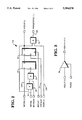
- FIG. 1 is a block diagram of a device for managing interrupt signals according to one form of the present invention.
- FIG. 2 is a circuit diagram of one register queue shown in FIG. 1.
- FIG. 3 is a circuit diagram of one status register shown in FIG. 1.
- FIG. 4 is a circuit diagram of the decoder shown in FIG. 1.
- FIG. 5 is a circuit diagram of the poll register shown in FIG. 1.
- FIG. 6 is a circuit diagram of the controller shown in FIG. 1.
- FIG. 1 shows a device 10 for managing multiple asynchronous interrupt signals SETIRQ(X) transmitted on lines 12.
- the notation "(X)" following a signal name indicates that a number of such signals are provided on respective individual lines.
- Device 10 includes register queues 14, a decoder 16, poll register 18, status registers 20 and controller 22.
- Device 10 is normally associated with a host processor and acts as an interrupt signal interface between various subsystems and the processor.
- the interrupt signals SETIRQ(X) are received from various subsystems, the system clock signal CLK and master reset signal MSTRRST/normally originate from the processor, and the interrupt signal IRQPIN is provided to the processor.
- the IRQEN(X) signals are associated on a one-to-one basis with the interrupt signals SETIRQ(X) and may be provided on lines 23 to selectively mask predetermined ones of said SETIRQ(X) signals.
- the halt signal HALT is a secondary interrupt that is generated in response to a so-called "fatal interrupt", such as a power failure, and may be made available to the processor or any subsystem needing the information.
- Read signal READ1 is provided by the processor to poll register 18, and read signal READ2 is provided by the system processor to status registers 20 and controller 22, as will be explained more fully.
- the signal IRQPOLL and signals IRQSTATUS(X) are provided to the processor in response to READ1 and READ2, respectively.
- FIG. 2 shows an exemplary queue 14a of register queues 14 which is connected to a single signal line 12a for receiving a single interrupt signal SETIRQ(1).
- register queue 14 includes a plurality of like elements to those shown in FIG. 2, one queue corresponding to each interrupt signal SETIRQ(X).
- Queue 14a includes a secondary register or SR latch 24 and a primary register or gated latch 26, with latch 24 connected between signal line 12a and latch 26. More particularly, the set input S of SR latch 24 is connected to signal line 12a for receiving SETIRQ(1).
- the SETIRQ(1) signal is also provided to the D input of latch 26 through the Q output of latch 24.
- the SETIRQ(1) signal is stored in primary register 26 in response to an OPENLAT/signal on its control gate G/ received from decoder 16 over line 27.
- the stored signal is provided on the Q output of latch 26 as the IRQOUT(1) signal.
- Queue 14a also includes 2-input coincidence gates in the form of NAND gates 28, 30 and 32.
- One input of NAND gate 28 is connected to the Q output of latch 26, and another input is connected to line 34 from controller 22 for receiving a reset signal RSTIRQ.
- the output of NAND gate 28 is provided to the reset R input of latch 24 through NAND gate 30.
- One input of NAND gate 30 is connected to the output of NAND gate 28, and another input receives the master reset signal MSTRRST/.
- NAND gate 30 The output of NAND gate 30 is connected to the reset R input of latch 24.
- One input of NAND gate 32 is connected to the Q output of latch 26, and the other input is connected to a single signal line 23a of lines 23 for receiving a single masking signal IRQEN(1), as will be described more fully.
- the output of NAND gate 32 provides a status bit ENIRQSTATUS(1)/ to decoder 16 over a single bit line 36a of a connector 36.
- queue 14a is but one of a plurality-of data bit queues contained within register queues 14. Since each queue is connected to a different input line 12 for receiving a different one of the interrupt signals SETIRQ(X), there is a primary and secondary register associated with each input line.
- Status registers 20 include a number of tristate gates, such as tristate gate 38 shown in FIG. 3.
- Tristate gate 38 receives the IRQOUT(1) signal from the Q output of primary register 26 (FIG. 2).
- Tristate gate 38 responds to the READ2/ signal by transferring the IRQOUT(1) input signal to its output as the IRQSTATUS(1) signal.
- FIG. 4 shows greater detail of decoder 16.
- decoder 16 is connected between the Q output of each primary register of register queues 14 and the G/gate of each such primary register.
- Decoder 16 receives the ENIRQSTATUS(X)/ signals from the Q outputs of primary registers 26 (FIG. 2) through NAND gate 32, provides to the system processor notice (IRQPIN) of stored signals in response, and changes the OPENLAT/signal to the G/input of primary registers 26 to close the primary registers to subsequently received SETIRQ(X) signals.
- IRQPIN system processor notice
- Synchronizer circuit 44 includes latches or D-type flip-flops 46, 48 and 50.
- the D input of flip-flop 46 is connected to a high voltage source, its clock input CK is connected to the output of inverter 42, and its Q output is connected to the D input of flip-flop 48.
- the Q output of flip-flop 48 is connected to the D input of flip-flop 50, and the clock inputs CK of both flip-flops 48 and 50 are connected to a system clock signal CLK.
- the Q output of flip-flop 50 provides the IRQPIN signal.
- Decoder 16 also includes inverter 56 and NOR GATE 58.
- the input of inverter 56 receives the master reset signal MSTRRST/and its output is connected to one of the inputs of NOR GATE 58.
- the other input of NOR GATE 58 receives a RSTIRQ signal from controller 22.
- the output of NOR GATE 58 is provided to the reset inputs R/of flip-flops 46, 48
- Decoder 16 further includes an SR latch 52 and an OR gate 60.
- the set input S of latch 52 is connected to the output of AND gate 40 through inverter 42, its reset input is connected to line 54 from controller 22 and receives the OPEN signal, and its Q output provides the gate control signal OPENLAT/ to the gates of primary registers 26.
- OR gate 60 receives IRQOUT(X) signals which have been predetermined to be fatal interrupts.
- the Q output of primary register 26 from queue 14a has been hardwired to one of the input of OR gate 60, thereby identifying its IRQOUT(1) signal as a fatal interrupt.
- the output of any other primary register 26 which will receive a fatal interrupt will be similarly hardwired as an input to OR gate 60.
- the output of OR gate 60 is the HALT signal.
- FIG. 5 shows poll register 18 which includes a tristate gate 62.
- Gate 62 receives the POLL signal from the Q output of flip-flop 50 (FIG. 4).
- Tristate gate 62 responds to the READ1/signal from the system processor by transferring the POLL signal to its output as the IRQPOLL signal.
- the IRQPOLL signal is provided to a polling device such as the system processor.
- FIG. 6 shows controller 22 which includes series connected D-type flip-flops 64, 66, 68 and 70, AND gate 72, NAND gates 74 and 76, inverter 78, and delay element 80.
- Flip-flop 64 receives the READ2/ signal from the system processor on its clock input CK, and the D input of flip-flop 64 is connected to a high voltage.
- the Q outputs of flip-flops 64, 66 and 68 are connected to the D inputs of flip-flops 66, 68 and 70, respectively.
- the Q/output of flip-flop 70 is provided to line 54 through NAND gate 76.
- Line 54 provides an OPEN signal to decoder 16 (FIG. 4) which signals decoder 16 to open the primary registers.
- NAND gate 76 receives the master reset signal MSTRRST/.
- the Q output of flip-flop 64 and the Q/output of intermediate flip-flop 68 are provided as inputs to AND gate 72.
- the output line 34 of AND gate 72 provides the RSTIRQ signal to register queues 14 (FIG. 2) and decoder 16 (FIG. 4).
- the Q output of flip-flop 68 and the Q/output of flip-flop 70 are provided as inputs to NAND GATE 74.
- the output of NAND gate 74 provides the RSTLAT/signal to register queues 14.
- the output of NAND gate 76 is also provided through inverter 78 and delay element 80 to the reset inputs R/of flip-flops 64, 66, 68 and 70.
- Each such device or subsystem has a dedicated interrupt line for providing a respective interrupt signal SETIRQ(X) to a respective register such as queue 14a (FIG. 2).
- Each SETIRQ(X) signal received by a register queue is provided to the S input of the respective secondary register 24.
- the stored signal is then provided on the Q output of register 24.
- the OPENLAT/signal is initially active so that the signal stored in register 24 is stored in primary register 26.
- the output of NAND gate 32 goes low if the IRQEN(1) bit has been set.
- the output of AND gate 40 (FIG.
- the Q output of latch 52 is the OPENLAT/ signal which when deactivated and provided to the G/ gate input of primary registers 26 (FIG. 2) closes registers 26 to subsequently received SETIRQ(X) signals.
- the first occurring of the SETIRQ(X) interrupt signals triggers the above sequence to close all primary registers 26.
- any other SETIRQ(X) signal occurring substantially simultaneously with the first occurring signal will also be stored in a respective primary register 26 prior to the closing of the registers 26.
- a SETIRQ(X) signal is received "substantially simultaneously” with a first occurring of such signals if it is received within the time required to deactivate the OPENLAT/ signal and close primary registers 26.
- SETIRQ(X) signals provided to register queues 14 after primary registers 26 are closed are stored in secondary registers 24.
- the output of inverter 42 is high after an interrupt signal is stored in a primary register.
- the inverter 42 output is applied to the CK input of flip-flop 46 which it clocks to a high value. This value is synchronized to the system clock signal CLK as it is sequentially latched into flip flops 48 and 50.
- the output of flip-flop 50 is the IRQPIN signal.
- the IRQPIN signal may be transmitted to the system processor as a synchronized interrupt signal (although synchronization may not be required in some systems).
- the signal is also stored in flip-flop 50 as a status bit. For systems where the processor polls device 16 for receipt of interrupt signals, flip-flop 50 may be read by the processor. This is done by a READ1/ signal being provided to tristate device 62 (FIG. 5).
- the processor reads each primary register 26 to identify each stored interrupt signal.
- the processor provides a READ2/signal, FIG. 3, to each tristate device 38 and receives the status of each primary register as an IRQSTATUS(X) signal. The processor can then proceed to service each interrupt.
- the READ2/signal is also provided to flip-flop 64, FIG. 6.
- the Q output of flip-flop 64 is provided to AND gate 72, the output of which is the RSTIRQ signal provided to an input of each NAND gate 28, FIG. 2.
- the other input of each NAND gate 28 is connected to the Q output of its respective primary register 26.
- the output of a NAND gate 28 will only go low when its respective primary register has a stored signal.
- a low output of a NAND gate 28 drives the output of NAND gate 30 high which resets secondary register 24.
- the Q output of flip-flop 68 is provided to NAND GATE 74, the output of which is the RSTLAT/signal provided to the reset R/input of all primary registers 26 (FIG. 2). This clears all the primary registers.
- the selected secondary registers 24 are cleared before the primary registers 26.
- the Q/output of flip-flop 68 and the Q/output of flip-flop 70 are provided to AND gate 72 and NAND GATE 74, respectively, to deactivate the RSTIRQ and RSTLAT/signals.
- the output of NAND gate 76, FIG. 6, is the OPEN signal which is provided to the reset input of latch 52, FIG. 4, to activate the OPENLAT/signal.
- the OPENLAT/ signal is provided to the G/gate of each primary register 26 (FIG. 2) to reopen primary registers 26 for the storage of any interrupt signals received after the primary registers were first closed. The processing of interrupt signals can continue as described above.
- Selected signals can be masked if notice of their receipt is not to be provided to the processor. This is achieved by deactivating the respective IRQEN(X) signal, FIG. 2. This keeps the output of the respective NAND gate 32 high irrespective of the output of its respective primary register 26.
- Certain signals may be predetermined to be fatal interrupts.
- the Q output of its respective primary register 26 is connected to OR gate 60, FIG. 4.
- the output of OR gate 60 is the HALT signal which provides priority notice of receipt of a fatal interrupt.
Landscapes
- Engineering & Computer Science (AREA)
- Theoretical Computer Science (AREA)
- Physics & Mathematics (AREA)
- General Engineering & Computer Science (AREA)
- General Physics & Mathematics (AREA)
- Bus Control (AREA)
Abstract
Description
Claims (22)
Priority Applications (1)
| Application Number | Priority Date | Filing Date | Title |
|---|---|---|---|
| US07/966,620 US5584028A (en) | 1990-05-14 | 1992-10-26 | Method and device for processing multiple, asynchronous interrupt signals |
Applications Claiming Priority (2)
| Application Number | Priority Date | Filing Date | Title |
|---|---|---|---|
| US52349190A | 1990-05-14 | 1990-05-14 | |
| US07/966,620 US5584028A (en) | 1990-05-14 | 1992-10-26 | Method and device for processing multiple, asynchronous interrupt signals |
Related Parent Applications (1)
| Application Number | Title | Priority Date | Filing Date |
|---|---|---|---|
| US52349190A Continuation | 1990-05-14 | 1990-05-14 |
Publications (1)
| Publication Number | Publication Date |
|---|---|
| US5584028A true US5584028A (en) | 1996-12-10 |
Family
ID=24085259
Family Applications (1)
| Application Number | Title | Priority Date | Filing Date |
|---|---|---|---|
| US07/966,620 Expired - Lifetime US5584028A (en) | 1990-05-14 | 1992-10-26 | Method and device for processing multiple, asynchronous interrupt signals |
Country Status (1)
| Country | Link |
|---|---|
| US (1) | US5584028A (en) |
Cited By (4)
| Publication number | Priority date | Publication date | Assignee | Title |
|---|---|---|---|---|
| US5857108A (en) * | 1995-11-21 | 1999-01-05 | Lg Semicon Co., Ltd. | Device and method for generating interrupts |
| DE10047183A1 (en) * | 2000-09-22 | 2002-04-18 | Infineon Technologies Ag | Intermediate digital memory element for transmitting flank signals from an interrupt generator to a CPU without any dead time being caused by the transfer |
| US6630926B2 (en) * | 2000-12-07 | 2003-10-07 | International Business Machines Corporation | Apparatus and method for verifying keystrokes within a computing system |
| US20040059439A1 (en) * | 2000-12-20 | 2004-03-25 | Rudiger Brunheim | Interrupt controller for a microprocessor |
Citations (27)
| Publication number | Priority date | Publication date | Assignee | Title |
|---|---|---|---|---|
| US3543242A (en) * | 1967-07-07 | 1970-11-24 | Ibm | Multiple level priority system |
| US3597743A (en) * | 1969-03-26 | 1971-08-03 | Digital Applic Inc | Expander for real-time communication between a computer and external devices |
| US3699530A (en) * | 1970-12-30 | 1972-10-17 | Ibm | Input/output system with dedicated channel buffering |
| US3829839A (en) * | 1972-07-24 | 1974-08-13 | California Inst Of Techn | Priority interrupt system |
| US3921145A (en) * | 1973-10-12 | 1975-11-18 | Burroughs Corp | Multirequest grouping computer interface |
| US4023143A (en) * | 1975-10-28 | 1977-05-10 | Cincinnati Milacron Inc. | Fixed priority interrupt control circuit |
| US4028667A (en) * | 1975-12-22 | 1977-06-07 | International Business Machines Corporation | Asynchronous, hierarchical loop communication system with independent local station control of access to inbound time portions without central control |
| US4041460A (en) * | 1975-05-17 | 1977-08-09 | Plessey Handel Und Investments Ag. | Multi-processor data processing system peripheral equipment access units |
| US4080649A (en) * | 1976-12-16 | 1978-03-21 | Honeywell Information Systems Inc. | Balancing the utilization of I/O system processors |
| US4091447A (en) * | 1976-07-19 | 1978-05-23 | Union Carbide Corporation | Interrupt control system for a microcomputer |
| US4153934A (en) * | 1976-02-10 | 1979-05-08 | Tokyo Shibaura Electric Co., Ltd. | Multiplex data processing system |
| US4215399A (en) * | 1978-08-24 | 1980-07-29 | Texas Instruments Incorporated | Special function control system for a dual microprocessor programmable process control system |
| US4215395A (en) * | 1978-08-24 | 1980-07-29 | Texas Instruments Incorporated | Dual microprocessor intelligent programmable process control system |
| US4220990A (en) * | 1978-09-25 | 1980-09-02 | Bell Telephone Laboratories, Incorporated | Peripheral processor multifunction timer for data processing systems |
| US4393470A (en) * | 1979-11-19 | 1983-07-12 | Compagnie Internationale Pour L'informatique Cii-Honeywell Bull (Societe Anonyme) | Method and device for the counting and management of asynchronous events emitted by peripheral devices in a data processing system |
| US4404648A (en) * | 1978-07-19 | 1983-09-13 | Hitachi, Ltd. | Method for controlling an instrument panel display |
| US4420806A (en) * | 1981-01-15 | 1983-12-13 | Harris Corporation | Interrupt coupling and monitoring system |
| US4494192A (en) * | 1982-07-21 | 1985-01-15 | Sperry Corporation | High speed bus architecture |
| US4626987A (en) * | 1982-09-10 | 1986-12-02 | U.S. Philips Corporation | Method of and circuit arrangement for supplying interrupt request signals |
| US4630041A (en) * | 1983-01-31 | 1986-12-16 | Honeywell Information Systems Italia | Enhanced reliability interrupt control apparatus |
| US4689739A (en) * | 1983-03-28 | 1987-08-25 | Xerox Corporation | Method for providing priority interrupts in an electrophotographic machine |
| US4734882A (en) * | 1985-04-01 | 1988-03-29 | Harris Corp. | Multilevel interrupt handling scheme |
| US4740915A (en) * | 1982-06-28 | 1988-04-26 | Robert Bosch Gmbh | Method of controlling a microprocessor to monitor input signals at irregular mutually intersecting intervals |
| US4799148A (en) * | 1984-10-30 | 1989-01-17 | Kabushiki Kaisha Toshiba | Interrupt control system having a processor for determining service priority among a plurality of modules according to an interrupt status table |
| US4835672A (en) * | 1984-04-02 | 1989-05-30 | Unisys Corporation | Access lock apparatus for use with a high performance storage unit of a digital data processing system |
| US5038275A (en) * | 1988-10-07 | 1991-08-06 | Advanced Micro Devices, Inc. | Status transfer structure within a data processing system with status read indication |
| US5043882A (en) * | 1989-03-03 | 1991-08-27 | Nec Corporation | Interrupt controller for multiprocessor systems |
-
1992
- 1992-10-26 US US07/966,620 patent/US5584028A/en not_active Expired - Lifetime
Patent Citations (27)
| Publication number | Priority date | Publication date | Assignee | Title |
|---|---|---|---|---|
| US3543242A (en) * | 1967-07-07 | 1970-11-24 | Ibm | Multiple level priority system |
| US3597743A (en) * | 1969-03-26 | 1971-08-03 | Digital Applic Inc | Expander for real-time communication between a computer and external devices |
| US3699530A (en) * | 1970-12-30 | 1972-10-17 | Ibm | Input/output system with dedicated channel buffering |
| US3829839A (en) * | 1972-07-24 | 1974-08-13 | California Inst Of Techn | Priority interrupt system |
| US3921145A (en) * | 1973-10-12 | 1975-11-18 | Burroughs Corp | Multirequest grouping computer interface |
| US4041460A (en) * | 1975-05-17 | 1977-08-09 | Plessey Handel Und Investments Ag. | Multi-processor data processing system peripheral equipment access units |
| US4023143A (en) * | 1975-10-28 | 1977-05-10 | Cincinnati Milacron Inc. | Fixed priority interrupt control circuit |
| US4028667A (en) * | 1975-12-22 | 1977-06-07 | International Business Machines Corporation | Asynchronous, hierarchical loop communication system with independent local station control of access to inbound time portions without central control |
| US4153934A (en) * | 1976-02-10 | 1979-05-08 | Tokyo Shibaura Electric Co., Ltd. | Multiplex data processing system |
| US4091447A (en) * | 1976-07-19 | 1978-05-23 | Union Carbide Corporation | Interrupt control system for a microcomputer |
| US4080649A (en) * | 1976-12-16 | 1978-03-21 | Honeywell Information Systems Inc. | Balancing the utilization of I/O system processors |
| US4404648A (en) * | 1978-07-19 | 1983-09-13 | Hitachi, Ltd. | Method for controlling an instrument panel display |
| US4215395A (en) * | 1978-08-24 | 1980-07-29 | Texas Instruments Incorporated | Dual microprocessor intelligent programmable process control system |
| US4215399A (en) * | 1978-08-24 | 1980-07-29 | Texas Instruments Incorporated | Special function control system for a dual microprocessor programmable process control system |
| US4220990A (en) * | 1978-09-25 | 1980-09-02 | Bell Telephone Laboratories, Incorporated | Peripheral processor multifunction timer for data processing systems |
| US4393470A (en) * | 1979-11-19 | 1983-07-12 | Compagnie Internationale Pour L'informatique Cii-Honeywell Bull (Societe Anonyme) | Method and device for the counting and management of asynchronous events emitted by peripheral devices in a data processing system |
| US4420806A (en) * | 1981-01-15 | 1983-12-13 | Harris Corporation | Interrupt coupling and monitoring system |
| US4740915A (en) * | 1982-06-28 | 1988-04-26 | Robert Bosch Gmbh | Method of controlling a microprocessor to monitor input signals at irregular mutually intersecting intervals |
| US4494192A (en) * | 1982-07-21 | 1985-01-15 | Sperry Corporation | High speed bus architecture |
| US4626987A (en) * | 1982-09-10 | 1986-12-02 | U.S. Philips Corporation | Method of and circuit arrangement for supplying interrupt request signals |
| US4630041A (en) * | 1983-01-31 | 1986-12-16 | Honeywell Information Systems Italia | Enhanced reliability interrupt control apparatus |
| US4689739A (en) * | 1983-03-28 | 1987-08-25 | Xerox Corporation | Method for providing priority interrupts in an electrophotographic machine |
| US4835672A (en) * | 1984-04-02 | 1989-05-30 | Unisys Corporation | Access lock apparatus for use with a high performance storage unit of a digital data processing system |
| US4799148A (en) * | 1984-10-30 | 1989-01-17 | Kabushiki Kaisha Toshiba | Interrupt control system having a processor for determining service priority among a plurality of modules according to an interrupt status table |
| US4734882A (en) * | 1985-04-01 | 1988-03-29 | Harris Corp. | Multilevel interrupt handling scheme |
| US5038275A (en) * | 1988-10-07 | 1991-08-06 | Advanced Micro Devices, Inc. | Status transfer structure within a data processing system with status read indication |
| US5043882A (en) * | 1989-03-03 | 1991-08-27 | Nec Corporation | Interrupt controller for multiprocessor systems |
Cited By (5)
| Publication number | Priority date | Publication date | Assignee | Title |
|---|---|---|---|---|
| US5857108A (en) * | 1995-11-21 | 1999-01-05 | Lg Semicon Co., Ltd. | Device and method for generating interrupts |
| DE10047183A1 (en) * | 2000-09-22 | 2002-04-18 | Infineon Technologies Ag | Intermediate digital memory element for transmitting flank signals from an interrupt generator to a CPU without any dead time being caused by the transfer |
| US6630926B2 (en) * | 2000-12-07 | 2003-10-07 | International Business Machines Corporation | Apparatus and method for verifying keystrokes within a computing system |
| US20040059439A1 (en) * | 2000-12-20 | 2004-03-25 | Rudiger Brunheim | Interrupt controller for a microprocessor |
| US20060168385A1 (en) * | 2000-12-20 | 2006-07-27 | Rudiger Brunheim | Interrupt controller for a microprocessor |
Similar Documents
| Publication | Publication Date | Title |
|---|---|---|
| CA1183273A (en) | Interface mechanism between a pair of processors, such as host and peripheral-controlling processors in data processing systems | |
| US5365485A (en) | Fifo with fast retransmit mode | |
| US6078970A (en) | System for determining adapter interrupt status where interrupt is sent to host after operating status stored in register is shadowed to host memory | |
| US3886524A (en) | Asynchronous communication bus | |
| US4275458A (en) | Interrupt expander circuit | |
| US5311475A (en) | High speed full and empty flag generators for first-in first-out memory | |
| US5355468A (en) | System for halting synchronous digital modules | |
| EP0196911A2 (en) | Local area networks | |
| US5297276A (en) | Method and apparatus for maintaining deterministic behavior in a first synchronous system which responds to inputs from nonsynchronous second system | |
| US5584028A (en) | Method and device for processing multiple, asynchronous interrupt signals | |
| EP0337993B1 (en) | Parallel processing state alignment | |
| US6286072B1 (en) | System and method for synchronizing data communication between asynchronous buses | |
| EP0492072A1 (en) | Data transfer bus system and method serving multiple parallel asynchronous units | |
| US3248707A (en) | Semi-asynchronous clock system | |
| JPS63123130A (en) | Pipeline control system | |
| CA1133088A (en) | Control system for input/output apparatus | |
| CA1309503C (en) | Selective receiver for each processor in a multiple processor system | |
| JPH11338712A (en) | Interruption sequence saving circuit | |
| JPS595331A (en) | Waiting system in magnetic disk subsystem | |
| JP2988139B2 (en) | Interrupt control device | |
| KR0162768B1 (en) | Queue synchronizing control circuit of interrupt processor in hipi + bus | |
| SU1116432A1 (en) | Firmware processor with fast interruption tools | |
| JPH04352057A (en) | Interruption information circuit | |
| GB2225460A (en) | Asynchronous interrupt arbitrator | |
| JPH10326194A (en) | Interruption control system |
Legal Events
| Date | Code | Title | Description |
|---|---|---|---|
| AS | Assignment |
Owner name: HYUNDAI ELECTRONICS AMERICA Free format text: ASSIGNMENT OF ASSIGNORS INTEREST;ASSIGNOR:AT&T GLOBAL INFORMATION SOLUTIONS COMPANY (FORMERLY KNOWN AS NCR CORPORATION);REEL/FRAME:007408/0104 Effective date: 19950215 |
|
| AS | Assignment |
Owner name: SYMBIOS LOGIC INC., COLORADO Free format text: ASSIGNMENT OF ASSIGNORS INTEREST;ASSIGNOR:HYUNDAI ELECTRONICS AMERICA;REEL/FRAME:007629/0431 Effective date: 19950818 |
|
| STCF | Information on status: patent grant |
Free format text: PATENTED CASE |
|
| AS | Assignment |
Owner name: SYMBIOS, INC ., COLORADO Free format text: CHANGE OF NAME;ASSIGNOR:SYMBIOS LOGIC INC.;REEL/FRAME:009089/0936 Effective date: 19971210 |
|
| AS | Assignment |
Owner name: LEHMAN COMMERCIAL PAPER INC., AS ADMINISTRATIVE AG Free format text: SECURITY AGREEMENT;ASSIGNORS:HYUNDAI ELECTRONICS AMERICA, A CORP. OF CALIFORNIA;SYMBIOS, INC., A CORP. OF DELAWARE;REEL/FRAME:009396/0441 Effective date: 19980226 |
|
| AS | Assignment |
Owner name: HYUNDAI ELECTRONICS AMERICA, CALIFORNIA Free format text: TERMINATION AND LICENSE AGREEMENT;ASSIGNOR:SYMBIOS, INC.;REEL/FRAME:009596/0539 Effective date: 19980806 |
|
| FEPP | Fee payment procedure |
Free format text: PAYOR NUMBER ASSIGNED (ORIGINAL EVENT CODE: ASPN); ENTITY STATUS OF PATENT OWNER: LARGE ENTITY |
|
| FPAY | Fee payment |
Year of fee payment: 4 |
|
| FPAY | Fee payment |
Year of fee payment: 8 |
|
| AS | Assignment |
Owner name: HYNIX SEMICONDUCTOR AMERICA INC., CALIFORNIA Free format text: CHANGE OF NAME;ASSIGNOR:HYUNDAI ELECTRONICS AMERICA;REEL/FRAME:015246/0599 Effective date: 20010412 Owner name: HYNIX SEMICONDUCTOR INC., KOREA, REPUBLIC OF Free format text: ASSIGNMENT OF ASSIGNORS INTEREST;ASSIGNOR:HYNIX SEMICONDUCTOR AMERICA, INC.;REEL/FRAME:015279/0556 Effective date: 20040920 |
|
| AS | Assignment |
Owner name: MAGNACHIP SEMICONDUCTOR, LTD., KOREA, REPUBLIC OF Free format text: ASSIGNMENT OF ASSIGNORS INTEREST;ASSIGNOR:HYNIX SEMICONDUCTOR, INC.;REEL/FRAME:016216/0649 Effective date: 20041004 |
|
| AS | Assignment |
Owner name: U.S. BANK NATIONAL ASSOCIATION, AS COLLATERAL TRUS Free format text: SECURITY INTEREST;ASSIGNOR:MAGNACHIP SEMICONDUCTOR, LTD.;REEL/FRAME:016470/0530 Effective date: 20041223 |
|
| AS | Assignment |
Owner name: SYMBIOS, INC., COLORADO Free format text: RELEASE OF SECURITY INTEREST;ASSIGNOR:LEHMAN COMMERICAL PAPER INC.;REEL/FRAME:016602/0895 Effective date: 20050107 Owner name: HYUNDAI ELECTRONICS AMERICA, CALIFORNIA Free format text: RELEASE OF SECURITY INTEREST;ASSIGNOR:LEHMAN COMMERICAL PAPER INC.;REEL/FRAME:016602/0895 Effective date: 20050107 |
|
| FPAY | Fee payment |
Year of fee payment: 12 |
|
| REMI | Maintenance fee reminder mailed | ||
| AS | Assignment |
Owner name: TAIWAN SEMICONDUCTOR MANUFACTURING CO., LTD., TAIW Free format text: ASSIGNMENT OF ASSIGNORS INTEREST;ASSIGNORS:NCR CORPORATION;MAGNACHIP SEMICONDUCTOR, LTD.;REEL/FRAME:021398/0702;SIGNING DATES FROM 20071114 TO 20071115 |