US5589415A - Method for forming a semiconductor structure with self-aligned contacts - Google Patents
Method for forming a semiconductor structure with self-aligned contacts Download PDFInfo
- Publication number
- US5589415A US5589415A US08/472,336 US47233695A US5589415A US 5589415 A US5589415 A US 5589415A US 47233695 A US47233695 A US 47233695A US 5589415 A US5589415 A US 5589415A
- Authority
- US
- United States
- Prior art keywords
- semiconductor layer
- layer
- portions
- polycrystalline semiconductor
- regions
- Prior art date
- Legal status (The legal status is an assumption and is not a legal conclusion. Google has not performed a legal analysis and makes no representation as to the accuracy of the status listed.)
- Expired - Lifetime
Links
- 238000000034 method Methods 0.000 title claims abstract description 31
- 239000004065 semiconductor Substances 0.000 title claims description 85
- 229910021420 polycrystalline silicon Inorganic materials 0.000 claims abstract description 52
- 229920005591 polysilicon Polymers 0.000 claims abstract description 52
- 238000005253 cladding Methods 0.000 claims abstract description 12
- 239000002019 doping agent Substances 0.000 claims description 26
- 238000004519 manufacturing process Methods 0.000 claims description 21
- 239000010409 thin film Substances 0.000 claims description 18
- 238000009792 diffusion process Methods 0.000 claims description 16
- 229910021332 silicide Inorganic materials 0.000 claims description 9
- 238000000151 deposition Methods 0.000 claims description 8
- 229910052751 metal Inorganic materials 0.000 claims description 6
- 239000002184 metal Substances 0.000 claims description 6
- 238000000059 patterning Methods 0.000 claims description 6
- FVBUAEGBCNSCDD-UHFFFAOYSA-N silicide(4-) Chemical compound [Si-4] FVBUAEGBCNSCDD-UHFFFAOYSA-N 0.000 claims description 6
- 125000006850 spacer group Chemical group 0.000 claims description 5
- 239000000463 material Substances 0.000 claims description 4
- 229910052710 silicon Inorganic materials 0.000 claims description 4
- 239000010703 silicon Substances 0.000 claims description 4
- 239000013078 crystal Substances 0.000 claims 1
- 239000007943 implant Substances 0.000 abstract description 12
- 230000008569 process Effects 0.000 abstract description 7
- ATJFFYVFTNAWJD-UHFFFAOYSA-N Tin Chemical compound [Sn] ATJFFYVFTNAWJD-UHFFFAOYSA-N 0.000 description 8
- ZOXJGFHDIHLPTG-UHFFFAOYSA-N Boron Chemical group [B] ZOXJGFHDIHLPTG-UHFFFAOYSA-N 0.000 description 2
- 229910052581 Si3N4 Inorganic materials 0.000 description 2
- VYPSYNLAJGMNEJ-UHFFFAOYSA-N Silicium dioxide Chemical compound O=[Si]=O VYPSYNLAJGMNEJ-UHFFFAOYSA-N 0.000 description 2
- XUIMIQQOPSSXEZ-UHFFFAOYSA-N Silicon Chemical compound [Si] XUIMIQQOPSSXEZ-UHFFFAOYSA-N 0.000 description 2
- 230000004888 barrier function Effects 0.000 description 2
- 230000008901 benefit Effects 0.000 description 2
- 229910052796 boron Inorganic materials 0.000 description 2
- 230000008021 deposition Effects 0.000 description 2
- 230000000694 effects Effects 0.000 description 2
- 230000005669 field effect Effects 0.000 description 2
- 230000036039 immunity Effects 0.000 description 2
- 230000003993 interaction Effects 0.000 description 2
- 239000000203 mixture Substances 0.000 description 2
- 230000003071 parasitic effect Effects 0.000 description 2
- HQVNEWCFYHHQES-UHFFFAOYSA-N silicon nitride Chemical compound N12[Si]34N5[Si]62N3[Si]51N64 HQVNEWCFYHHQES-UHFFFAOYSA-N 0.000 description 2
- 239000010936 titanium Substances 0.000 description 2
- FTVWIRXFELQLPI-ZDUSSCGKSA-N (S)-naringenin Chemical compound C1=CC(O)=CC=C1[C@H]1OC2=CC(O)=CC(O)=C2C(=O)C1 FTVWIRXFELQLPI-ZDUSSCGKSA-N 0.000 description 1
- ZOKXTWBITQBERF-UHFFFAOYSA-N Molybdenum Chemical compound [Mo] ZOKXTWBITQBERF-UHFFFAOYSA-N 0.000 description 1
- 230000015556 catabolic process Effects 0.000 description 1
- 230000000295 complement effect Effects 0.000 description 1
- 238000013500 data storage Methods 0.000 description 1
- 238000005530 etching Methods 0.000 description 1
- 230000006870 function Effects 0.000 description 1
- 238000010438 heat treatment Methods 0.000 description 1
- 238000002513 implantation Methods 0.000 description 1
- 238000005468 ion implantation Methods 0.000 description 1
- 238000002955 isolation Methods 0.000 description 1
- 230000000873 masking effect Effects 0.000 description 1
- 238000012986 modification Methods 0.000 description 1
- 230000004048 modification Effects 0.000 description 1
- 229910052750 molybdenum Inorganic materials 0.000 description 1
- 239000011733 molybdenum Substances 0.000 description 1
- 150000004767 nitrides Chemical class 0.000 description 1
- 238000002161 passivation Methods 0.000 description 1
- 230000001681 protective effect Effects 0.000 description 1
- 235000012239 silicon dioxide Nutrition 0.000 description 1
- 239000000377 silicon dioxide Substances 0.000 description 1
- 239000000758 substrate Substances 0.000 description 1
- 229910052715 tantalum Inorganic materials 0.000 description 1
- GUVRBAGPIYLISA-UHFFFAOYSA-N tantalum atom Chemical compound [Ta] GUVRBAGPIYLISA-UHFFFAOYSA-N 0.000 description 1
- 229910021341 titanium silicide Inorganic materials 0.000 description 1
- 230000001052 transient effect Effects 0.000 description 1
- 230000007704 transition Effects 0.000 description 1
Images


Classifications
-
- H—ELECTRICITY
- H01—ELECTRIC ELEMENTS
- H01L—SEMICONDUCTOR DEVICES NOT COVERED BY CLASS H10
- H01L29/00—Semiconductor devices adapted for rectifying, amplifying, oscillating or switching, or capacitors or resistors with at least one potential-jump barrier or surface barrier, e.g. PN junction depletion layer or carrier concentration layer; Details of semiconductor bodies or of electrodes thereof ; Multistep manufacturing processes therefor
- H01L29/66—Types of semiconductor device ; Multistep manufacturing processes therefor
- H01L29/66007—Multistep manufacturing processes
- H01L29/66075—Multistep manufacturing processes of devices having semiconductor bodies comprising group 14 or group 13/15 materials
- H01L29/66227—Multistep manufacturing processes of devices having semiconductor bodies comprising group 14 or group 13/15 materials the devices being controllable only by the electric current supplied or the electric potential applied, to an electrode which does not carry the current to be rectified, amplified or switched, e.g. three-terminal devices
- H01L29/66409—Unipolar field-effect transistors
- H01L29/66477—Unipolar field-effect transistors with an insulated gate, i.e. MISFET
- H01L29/66568—Lateral single gate silicon transistors
- H01L29/66659—Lateral single gate silicon transistors with asymmetry in the channel direction, e.g. lateral high-voltage MISFETs with drain offset region, extended drain MISFETs
-
- H—ELECTRICITY
- H01—ELECTRIC ELEMENTS
- H01L—SEMICONDUCTOR DEVICES NOT COVERED BY CLASS H10
- H01L21/00—Processes or apparatus adapted for the manufacture or treatment of semiconductor or solid state devices or of parts thereof
- H01L21/70—Manufacture or treatment of devices consisting of a plurality of solid state components formed in or on a common substrate or of parts thereof; Manufacture of integrated circuit devices or of parts thereof
- H01L21/71—Manufacture of specific parts of devices defined in group H01L21/70
- H01L21/768—Applying interconnections to be used for carrying current between separate components within a device comprising conductors and dielectrics
- H01L21/76838—Applying interconnections to be used for carrying current between separate components within a device comprising conductors and dielectrics characterised by the formation and the after-treatment of the conductors
- H01L21/76886—Modifying permanently or temporarily the pattern or the conductivity of conductive members, e.g. formation of alloys, reduction of contact resistances
- H01L21/76889—Modifying permanently or temporarily the pattern or the conductivity of conductive members, e.g. formation of alloys, reduction of contact resistances by forming silicides of refractory metals
-
- H—ELECTRICITY
- H01—ELECTRIC ELEMENTS
- H01L—SEMICONDUCTOR DEVICES NOT COVERED BY CLASS H10
- H01L21/00—Processes or apparatus adapted for the manufacture or treatment of semiconductor or solid state devices or of parts thereof
- H01L21/70—Manufacture or treatment of devices consisting of a plurality of solid state components formed in or on a common substrate or of parts thereof; Manufacture of integrated circuit devices or of parts thereof
- H01L21/77—Manufacture or treatment of devices consisting of a plurality of solid state components or integrated circuits formed in, or on, a common substrate
- H01L21/78—Manufacture or treatment of devices consisting of a plurality of solid state components or integrated circuits formed in, or on, a common substrate with subsequent division of the substrate into plural individual devices
- H01L21/82—Manufacture or treatment of devices consisting of a plurality of solid state components or integrated circuits formed in, or on, a common substrate with subsequent division of the substrate into plural individual devices to produce devices, e.g. integrated circuits, each consisting of a plurality of components
- H01L21/822—Manufacture or treatment of devices consisting of a plurality of solid state components or integrated circuits formed in, or on, a common substrate with subsequent division of the substrate into plural individual devices to produce devices, e.g. integrated circuits, each consisting of a plurality of components the substrate being a semiconductor, using silicon technology
- H01L21/8232—Field-effect technology
- H01L21/8234—MIS technology, i.e. integration processes of field effect transistors of the conductor-insulator-semiconductor type
- H01L21/8238—Complementary field-effect transistors, e.g. CMOS
- H01L21/823871—Complementary field-effect transistors, e.g. CMOS interconnection or wiring or contact manufacturing related aspects
-
- H—ELECTRICITY
- H01—ELECTRIC ELEMENTS
- H01L—SEMICONDUCTOR DEVICES NOT COVERED BY CLASS H10
- H01L29/00—Semiconductor devices adapted for rectifying, amplifying, oscillating or switching, or capacitors or resistors with at least one potential-jump barrier or surface barrier, e.g. PN junction depletion layer or carrier concentration layer; Details of semiconductor bodies or of electrodes thereof ; Multistep manufacturing processes therefor
- H01L29/66—Types of semiconductor device ; Multistep manufacturing processes therefor
- H01L29/68—Types of semiconductor device ; Multistep manufacturing processes therefor controllable by only the electric current supplied, or only the electric potential applied, to an electrode which does not carry the current to be rectified, amplified or switched
- H01L29/76—Unipolar devices, e.g. field effect transistors
- H01L29/772—Field effect transistors
- H01L29/78—Field effect transistors with field effect produced by an insulated gate
- H01L29/7833—Field effect transistors with field effect produced by an insulated gate with lightly doped drain or source extension, e.g. LDD MOSFET's; DDD MOSFET's
- H01L29/7835—Field effect transistors with field effect produced by an insulated gate with lightly doped drain or source extension, e.g. LDD MOSFET's; DDD MOSFET's with asymmetrical source and drain regions, e.g. lateral high-voltage MISFETs with drain offset region, extended drain MISFETs
-
- Y—GENERAL TAGGING OF NEW TECHNOLOGICAL DEVELOPMENTS; GENERAL TAGGING OF CROSS-SECTIONAL TECHNOLOGIES SPANNING OVER SEVERAL SECTIONS OF THE IPC; TECHNICAL SUBJECTS COVERED BY FORMER USPC CROSS-REFERENCE ART COLLECTIONS [XRACs] AND DIGESTS
- Y10—TECHNICAL SUBJECTS COVERED BY FORMER USPC
- Y10S—TECHNICAL SUBJECTS COVERED BY FORMER USPC CROSS-REFERENCE ART COLLECTIONS [XRACs] AND DIGESTS
- Y10S257/00—Active solid-state devices, e.g. transistors, solid-state diodes
- Y10S257/903—FET configuration adapted for use as static memory cell
Definitions
- the present application relates to device structures and fabrication processes for high-density integrated circuits.
- CMOS devices In CMOS devices, one of the limitations on this is that diffusion between n+ and p+ regions may cause counterdoping (where p-type and n-type dopant contributions offset each other). Counterdoping may cause increased resistance (since the effective doping will become lower), and may even cause changes in the device threshold voltage if the counterdoping affects the polysilicon doping over a transistor channel.
- polysilicon is doped n+ (as is most common), then a direct connection between polysilicon and a PMOS drain region will form a diode, which will be inherently susceptible to counterdoping effects.
- One approach to this is to interpose a diffusion barrier (e.g. TiN) between the polysilicon and the p+ drain regions.
- a diffusion barrier e.g. TiN
- silicides A further complication is dopant diffusion through silicides: common dopants may diffuse very rapidly in commonly used silicides. Silicides are often used to strap polysilicon layers, but lateral diffusion through the silicide increases the counterdoping problems.
- n+ polysilicon provides the gates of NMOS devices
- p+ polysilicon provides the gates of PMOS devices. Junctions between n+ and p+ may be avoided (by resorting to metal jumpers to make connection), or may be shunted by metal or silicide strapping. See e.g. U.S. Pat. Nos. 4,985,746 to Asahina and 3,673,471 to Klein et al.
- the present application provides new local interconnect structures and processes using dual-doped polysilicon.
- a single implant dopes part of the polysilicon local interconnect layer p-type, and also diffuses through the polysilicon interconnect layer to enhance the doping of the PMOS drain regions, and also (optionally) adds to the doping of the PMOS source regions to provide source/drain asymmetry.
- the polysilicon interconnect layer is clad to reduce its conductivity, e.g. by being salicided.
- the cladding which shunts the lateral polysilicon junction is patterned rather than global, so that the diode can be used as a load element if desired.
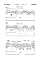
- FIGS. 1A-1F show fabrication steps in a first innovative embodiment.
- FIGS. 2A-2F show fabrication steps in a second innovative embodiment.
- FIGS. 3A-3F show fabrication steps in a third innovative embodiment.
- FIG. 4 shows how an SRAM cell core (latch) according to the disclosed innovations can include or omit junction diodes.
- FIG. 5 is a sectional view showing how dual-doped poly interconnects, fabricated according to one of the process sequences ending in FIGS. 1F, 2F, or 3F, permit a junction diode to be optionally avoided when metallic strapping is used.
- FIGS. 1A-1F show fabrication steps in a first innovative embodiment.
- FIG. 1A shows a structure after conventional initial processing steps.
- An n- substrate 102 has P-well regions 104 diffused into it, and a patterned field oxide 106 provides isolation separating the various active areas 108.
- a first patterned polysilicon layer 110 runs across the active areas 108 and field oxide 106, and provides transistor gates wherever it crosses an active area.
- Sidewall spacers 111 which may be silicon dioxide or silicon nitride, are preferably formed on the first poly layer 110 as shown.
- An interpoly dielectric 112 e.g. a conventional deposited oxide or ONO dielectric
- the patterning removes dielectric 112 from locations 107 where poly-to-poly contacts will be located, as well as from PMOS source/drain locations. Also note that a relatively thin grown oxide 109 remains at the silicon surface in locations where PMOS devices will be formed. This completes fabrication of the intermediate structure of FIG. 1A.
- the oxide 109 is then removed from PMOS drain regions 114 (but not from the source regions 116), preferably using an etch which is at least partially self-aligned. (Thus the sidewall spacers 111, as well as the top surface of the interpoly dielectric 112, are preferably formed of silicon nitride, to permit selective oxide etching.) This completes fabrication of the intermediate structure of FIG. 1C.
- a second layer of polysilicon 120 is now deposited, in a substantially intrinsic (or at most lightly doped) condition, with a thickness of e.g. 3000 ⁇ , and patterned to form desired connections, e.g. from poly-to-poly contacts 107 to PMOS drains 114. This completes fabrication of the intermediate structure of FIG. 1D.
- a mask is now used to implant a heavy dose of p-type dopants into areas 122.
- This includes PMOS source and drain regions, and portions of the second polysilicon layer 120 which are adjacent to PMOS source or drain regions.
- the entire right side of the illustrated section is part of such an area 122.
- This implant produces p-type polysilicon 120P in the areas of poly 120 which lie within the areas 122.
- This implant is preferably boron, implanted e.g. with BF 2 at an areal density of 5 ⁇ 10 14 -5 ⁇ 10 15 cm -2 and an energy of 50-200 keV (or alternatively with boron at an energy of 30-100 keV). (Note that this energy is selected to penetrate the oxide 109 over the drain regions 116.) (Alternatively, the oxide 109 may be stripped before this implant. This is easier if the sidewall spacers 111 are nitride.)
- a diffusion step is now performed (e.g. by a rapid thermal anneal step to a peak temperature of 800°-1000° C. for 60-900 seconds). This diffusion step performs three functions:
- effects 2 and 3 provide an asymmetrical LDD structure in the PMOS devices.
- the density (atoms per unit area) of the added dopant concentration 116" in the PMOS source regions is much heavier than that of the added dopant concentration 114' in the PMOS drain regions 114. This is advantageous for several reasons:
- the source regions will have a lower sheet resistance, and hence are useful for Vss and signal routing.
- the wider p- extent on the drain side provides protection against hot hole generation, if dimensions and operating voltages are such that hot holes are a concern.
- N-type dopants are now implanted into regions 124, to form N-type polysilicon 120N in those areas (and define the lateral junction 126 between N-type poly 120N and P-type poly 120P).
- the surface of the polysilicon is now clad with a conductive layer 130. This can be done in several ways.
- the conductive layer is simply deposited and patterned, e.g. as 500 ⁇ CVD W over 200 ⁇ CVD TiN.
- other compositions can be used for the conductive layer 130, e.g. molybdenum or another metal, or tantalum or another silicide, alone or over TiN.
- a salicidation step can be performed at this point, e.g. by depositing Ti overall, briefly heating (RTA) to form titanium silicide on exposed silicon and polysilicon, and stripping the Ti or TiN from dielectric areas.
- RTA briefly heating
- the polysilicon 120 can be initially deposited as a layered structure (e.g. 400 ⁇ TiN over 2000 ⁇ of polysilicon). However, this will require a higher dose and/or energy for the implants which dope the polysilicon, and this must be balanced against the maximum desired depth of the added dopant concentration 116" in the PMOS source regions.
- option 1 An important advantage of option 1 is that the conductive layer can optionally be omitted over the junction 126.
- This junction 126 then provides designers with an optional load element which can be used, in combination with a CMOS gate, to reduce the charge consumption during a transition. Since polysilicon diodes tend to be leaky, this junction 126 can also be used to provide a very high-impedance load, e.g. for output latches with added ESD resistance, if desired.
- a passivation layer 132 is then deposited over the conductive layer. This completes fabrication of the intermediate structure of FIG. 1F. Processing now concludes with conventional steps, e.g. contact etch, deposition and etch of one or more metal layers, and deposition and etch of a protective overcoat layer.
- the foregoing description has concentrated on the interaction between P+ doping of the second polysilicon layer 120 and the PMOS source and drain regions.
- the second polysilicon layer 120 also makes contact to NMOS drain regions, and the same process steps can advantageously provide modified NMOS source and drain doping while the second polysilicon layer 120 is being doped.
- FIGS. 2A-2F show fabrication steps in a second innovative embodiment. This embodiment is generally quite similar to the first embodiment, except that the PMOS source and drain regions in this embodiment are identical.
- FIGS. 2A-2C are identical to FIGS. 1A-1C, and the processing steps are also identical.
- the second polysilicon layer 120 is not removed from the PMOS source regions when it is etched.
- the added doping concentration 116' in the PMOS source regions therefore has a profile which is identical to that of the added doping concentration 114' in the PMOS drain regions.
- the remaining processing steps can be identical to those used in the primary embodiment (and its variations).
- the conductive layer 130 is not used to contact the PMOS source regions in this embodiments, selection of materials for the conductive layer 130 is somewhat less critical.
- the foregoing description has concentrated on the interaction between P+ doping of the second polysilicon layer 120 and the PMOS source and drain regions.
- the second polysilicon layer 120 also makes contact to NMOS drain regions, and the same process steps can advantageously provide modified NMOS source and drain doping while the second polysilicon layer 120 is being doped.
- FIGS. 3A-3F show fabrication steps in a third innovative embodiment. This embodiment is somewhat less similar to the first embodiment.
- FIGS. 3A-3B are identical to FIGS. 1A-1B, and the processing steps are also identical. However, this embodiment does not use a dual-doped polysilicon layer. Instead, as seen in FIG. 3C, when the second polysilicon layer 120 is etched it is removed from PMOS source and drain regions. This embodiment may be attractive in embodiments where the second polysilicon layer is needed for other reasons, e.g. to provide increased layout density in some parts of the chip.
- FIG. 4 shows how an SRAM cell can include or omit junction diodes (related to the need to connect from N+ to P+), depending on whether strapping is used.
- NMOS transistor 70 and PMOS transistor 66 provide one inverter
- NMOS transistor 72 and PMOS transistor 68 provide another inverter.
- the two inverters are cross-coupled, i.e. the input of either inverter is connected to the output of the other. This provides a positive-feedback relation with two stable states, and hence data storage is possible.
- each PMOS transistor is necessarily P-type, and the drain of each NMOS transistor is necessarily N-type.
- the gate polysilicon is also normally N-type.
- a junction 80 it is possible (e.g. if first contacts are used) for a junction 80 to exist between the drain of PMOS 68 and the drain of NMOS 72 (which also provides the first output node 76).
- a junction 78 it is possible for a junction 78 to exist between the drain of PMOS 66 and the drain of NMOS 70 (which also provides the second output node 74).
- the use of ohmic contacts to bridge these junctions e.g. by using cladding as shown in FIG. 5, shorts out the junctions 76 and 78.
- FIG. 5 is a sectional view showing how dual-doped poly interconnects, fabricated according to one of the process sequences ending in FIGS. 1F, 2F, or 3F, permit a junction diode to be optionally avoided when metallic strapping is used.
- a first N-type poly layer 46 provides insulated transistor gates over N-well regions 38 and over P-well regions 36.
- a second poly layer has N-type regions 58 and P-type regions 56, separated by a lateral junction 60.
- P-type polysilicon regions 56 make contact to P+ source/drain diffusions, and N-type regions 58 make contact to N+ source/drain diffusions (not shown in this Figure).
- Cladding 62 makes ohmic contact to both N-type regions 58 and P-type regions 56, and hence shunts the junction 60.
- the cladding 62 may be a salicide, or may be self-aligned (direct-reacted) TiN, or may be a deposited structure such as W over TiN.
- a fabrication method comprising the steps of: forming a first patterned thin-film polycrystalline semiconductor layer to provide insulated gates over first and second crystalline semiconductor regions, the second semiconductor region having a first conductivity type and the first semiconductor region having a second conductivity type; forming an interlevel dielectric over the first polycrystalline semiconductor layer; depositing a second polycrystalline semiconductor layer which at least partly overlies the interlevel dielectric, and patterning the second polycrystalline layer to expose at least some portions of the first and second semiconductor regions; doping a first portion of the second polycrystalline layer with first-conductivity-type dopants, and simultaneously doping any exposed portions of the first semiconductor regions; doping a second portion of the second polycrystalline semiconductor layer with second-conductivity-type dopants, and simultaneously doping any exposed portions of the second semiconductor regions; and cladding the second polycrystalline semiconductor layer with a layer of metallic conductivity which shunts at least some of the lateral junctions.
- a fabrication method comprising the steps of: forming a first patterned thin-film polycrystalline semiconductor layer to provide insulated gates over first and second crystalline semiconductor regions, the second semiconductor region having a first conductivity type and the first semiconductor region having a second conductivity type, and forming preliminary diffusions of the first conductivity type in the first semiconductor region and of the second conductivity type in the second semiconductor region, the preliminary diffusions being at least partly self-aligned to the first layer; forming a patterned interlevel dielectric over the first polycrystalline semiconductor layer; depositing a second polycrystalline semiconductor layer which at least partly overlies the interlevel dielectric, and patterning the second polycrystalline semiconductor layer to expose at least some portions of the first and second semiconductor regions; doping a first portion of the second polycrystalline semiconductor layer with first-conductivity-type dopants, and simultaneously doping any exposed portions of the first semiconductor regions; and doping a second portion of the second polycrystalline semiconductor layer with second-conductivity-type dopants.
- a fabrication method comprising the steps of: forming a first patterned thin-film polycrystalline semiconductor layer to provide insulated gates over first and second crystalline semiconductor regions; forming an interlevel dielectric over the first polycrystalline semiconductor layer, and patterning the interlevel dielectric layer to expose at least some portions of the first and second semiconductor regions; depositing a second polycrystalline semiconductor layer which at least partly overlies the interlevel dielectric; doping a first portion of the second polycrystalline layer with first-conductivity-type dopants, and diffusing the first-conductivity-type dopants into the first crystalline semiconductor region to form diffusions therein; and doping a second portion of the second polycrystalline semiconductor layer with second-conductivity-type dopants, and diffusing the second-conductivity-type dopants into the second crystalline semiconductor region to form diffusions therein.
- a fabrication method comprising the steps of: forming a first patterned thin-film polycrystalline semiconductor layer to provide insulated gates over first and second crystalline semiconductor regions; forming a patterned interlevel dielectric over the first polycrystalline semiconductor layer; forming a patterned second polycrystalline semiconductor layer to expose the first semiconductor regions; doping a first portion of the second polycrystalline layer with first-conductivity-type dopants, and simultaneously doping any exposed portions of the first semiconductor regions; and forming an additional patterned layer of metallic conductivity, having a composition different from the second polycrystalline semiconductor layer, to make ohmic connections from the second polycrystalline semiconductor layer to the first semiconductor regions.
- An integrated circuit comprising: first field-effect transistors having gates thereof formed in a first patterned thin-film polycrystalline semiconductor layer, and having source and drain regions of a first conductivity type; second field-effect transistors having gates thereof formed in the first patterned thin-film polycrystalline semiconductor layer, and having source and drain regions of a second conductivity type; a second patterned thin-film polycrystalline semiconductor layer, including first portions with the first conductivity type, second portions with the second conductivity type, and lateral junctions between the first and second portions; the second polycrystalline semiconductor layer being clad by a layer of metallic conductivity which shunts at least some of the lateral junctions; at least one the transistor having a dopant profile in the source region thereof which is different from the dopant profile in the drain region thereof.
- two masked implants are preferably used to implant the dual-doped polysilicon layer, but alternatively and less preferably counterdoping can be used here to save a mask (i.e. one implant is performed as a blanket implant).
- the N-type and P-type poly regions do not have to be fully complementary patterns; some of the second polysilicon can be left intrinsic if desired, to provide high-resistivity material for resistors or loads.
- the present invention can be applied to fabrication of the N-channel devices in addition to or instead of the application to P-channel devices which is discussed in detail above.
- the process steps describe above can then provide LDD asymmetry between NMOS source and drain, which is useful for optimal hot-carrier control with maximum drive capability.
- the strapping between the N-type and P-type polysilicon regions can use various known materials, such as TiN or TiW, in addition to the use of a silicide.
- the fabrication steps discussed above can optionally be performed selectively, in the periphery and not in the memory array of a memory chip.
Abstract
Local interconnect structures and processes using dual-doped polysilicon. A single implant dopes part of the polysilicon local interconnect layer p-type, and also diffuses through the polysilicon interconnect layer to enhance the doping of the PMOS drain regions, and also (optionally) adds to the doping of the PMOS source regions to provide source/drain asymmetry. The polysilicon interconnect layer is clad to reduce its conductivity, optionally with patterned rather than global cladding so that the diode can be used as a load element if desired.
Description
The present application relates to device structures and fabrication processes for high-density integrated circuits.
In integrated circuit device structures, it is often convenient to use polysilicon to form local interconnects. This is particularly attractive in SRAM cells, where the cross-coupled inverters require at least two gate-to-drain connections: if these connections can be implemented without using metal, layout is simplified.
In CMOS devices, one of the limitations on this is that diffusion between n+ and p+ regions may cause counterdoping (where p-type and n-type dopant contributions offset each other). Counterdoping may cause increased resistance (since the effective doping will become lower), and may even cause changes in the device threshold voltage if the counterdoping affects the polysilicon doping over a transistor channel.
If polysilicon is doped n+ (as is most common), then a direct connection between polysilicon and a PMOS drain region will form a diode, which will be inherently susceptible to counterdoping effects.
One approach to this is to interpose a diffusion barrier (e.g. TiN) between the polysilicon and the p+ drain regions. However, this is not possible in all processes.
A further complication is dopant diffusion through silicides: common dopants may diffuse very rapidly in commonly used silicides. Silicides are often used to strap polysilicon layers, but lateral diffusion through the silicide increases the counterdoping problems.
Many papers have proposed use of polysilicon with two doping types: n+ polysilicon provides the gates of NMOS devices, and p+ polysilicon provides the gates of PMOS devices. Junctions between n+ and p+ may be avoided (by resorting to metal jumpers to make connection), or may be shunted by metal or silicide strapping. See e.g. U.S. Pat. Nos. 4,985,746 to Asahina and 3,673,471 to Klein et al.
Commonly-owned U.S. Pat. No. 5,478,771 which is hereby incorporated by reference, disclosed a process using polysilicon for local interconnect, wherein masked implantation of the second polysilicon layer is used to assure that p+/n+ junctions are located as lateral junctions in the second polysilicon layer rather than at the contact to PMOS source/drain regions. Silicide cladding is then applied to short out these lateral junctions.
The present application provides new local interconnect structures and processes using dual-doped polysilicon. A single implant dopes part of the polysilicon local interconnect layer p-type, and also diffuses through the polysilicon interconnect layer to enhance the doping of the PMOS drain regions, and also (optionally) adds to the doping of the PMOS source regions to provide source/drain asymmetry.
The polysilicon interconnect layer is clad to reduce its conductivity, e.g. by being salicided. Optionally, the cladding which shunts the lateral polysilicon junction is patterned rather than global, so that the diode can be used as a load element if desired.
The disclosed inventions will be described with reference to the accompanying drawings, which show important sample embodiments of the invention and which are incorporated in the specification hereof by reference, wherein:
FIGS. 1A-1F show fabrication steps in a first innovative embodiment.
FIGS. 2A-2F show fabrication steps in a second innovative embodiment.
FIGS. 3A-3F show fabrication steps in a third innovative embodiment.
FIG. 4 shows how an SRAM cell core (latch) according to the disclosed innovations can include or omit junction diodes.
FIG. 5 is a sectional view showing how dual-doped poly interconnects, fabricated according to one of the process sequences ending in FIGS. 1F, 2F, or 3F, permit a junction diode to be optionally avoided when metallic strapping is used.
The numerous innovative teachings of the present application will be described with particular reference to the presently preferred embodiment (by way of example, and not of limitation), in which:
Primary Embodiment
FIGS. 1A-1F show fabrication steps in a first innovative embodiment.
FIG. 1A shows a structure after conventional initial processing steps. An n- substrate 102 has P-well regions 104 diffused into it, and a patterned field oxide 106 provides isolation separating the various active areas 108. A first patterned polysilicon layer 110 runs across the active areas 108 and field oxide 106, and provides transistor gates wherever it crosses an active area. (Sidewall spacers 111, which may be silicon dioxide or silicon nitride, are preferably formed on the first poly layer 110 as shown.) An interpoly dielectric 112 (e.g. a conventional deposited oxide or ONO dielectric) is then deposited and patterned. Note that the patterning removes dielectric 112 from locations 107 where poly-to-poly contacts will be located, as well as from PMOS source/drain locations. Also note that a relatively thin grown oxide 109 remains at the silicon surface in locations where PMOS devices will be formed. This completes fabrication of the intermediate structure of FIG. 1A.
Doping of PMOS source and drain regions is now begun using ion implantation and drive-in, e.g. with a dose of 5×10¹³ -5×1014 cm-2 and energy which produces P-type drain regions 114 and source regions 116 with an eventual junction depth of e.g. 0.3-1.5 μm. This completes fabrication of the intermediate structure of FIG. 1B.
The oxide 109 is then removed from PMOS drain regions 114 (but not from the source regions 116), preferably using an etch which is at least partially self-aligned. (Thus the sidewall spacers 111, as well as the top surface of the interpoly dielectric 112, are preferably formed of silicon nitride, to permit selective oxide etching.) This completes fabrication of the intermediate structure of FIG. 1C.
A second layer of polysilicon 120 is now deposited, in a substantially intrinsic (or at most lightly doped) condition, with a thickness of e.g. 3000 Å, and patterned to form desired connections, e.g. from poly-to-poly contacts 107 to PMOS drains 114. This completes fabrication of the intermediate structure of FIG. 1D.
A mask is now used to implant a heavy dose of p-type dopants into areas 122. This includes PMOS source and drain regions, and portions of the second polysilicon layer 120 which are adjacent to PMOS source or drain regions. In the figures the entire right side of the illustrated section (to the right of the lateral junction 126) is part of such an area 122. This implant produces p-type polysilicon 120P in the areas of poly 120 which lie within the areas 122. This implant is preferably boron, implanted e.g. with BF2 at an areal density of 5×10¹⁴ -5×1015 cm-2 and an energy of 50-200 keV (or alternatively with boron at an energy of 30-100 keV). (Note that this energy is selected to penetrate the oxide 109 over the drain regions 116.) (Alternatively, the oxide 109 may be stripped before this implant. This is easier if the sidewall spacers 111 are nitride.)
A diffusion step is now performed (e.g. by a rapid thermal anneal step to a peak temperature of 800°-1000° C. for 60-900 seconds). This diffusion step performs three functions:
1) it dopes (and activates the doping in) the p-type polysilicon 120P;
2) it adds additional dopant 116" to the PMOS source regions 116; and
3) it adds additional dopant 114' to the PMOS drain regions 114.
Note that effects 2 and 3 provide an asymmetrical LDD structure in the PMOS devices. In particular, the density (atoms per unit area) of the added dopant concentration 116" in the PMOS source regions is much heavier than that of the added dopant concentration 114' in the PMOS drain regions 114. This is advantageous for several reasons:
1) The source regions will have a lower sheet resistance, and hence are useful for Vss and signal routing.
2) The added dopant concentration 114' in the PMOS drain regions will be sufficient to provide a reasonably low specific contact resistance (ohm-cm2).
3) The wider p- extent on the drain side provides reduced parasitic capacitance on drain diffusions.
4) The wider p- extent on the drain side provides protection against hot hole generation, if dimensions and operating voltages are such that hot holes are a concern.
5) The wider p- extent on the drain side provides slightly improved junction leakage.
6) The wider p- extent on the drain side provides better immunity to breakdown under transient overvoltages.
7) The wider p- extent on the drain side provides reduced emitter efficiency, and some added series resistance, in the PNP component of the parasitic thyristor, and hence provides some added immunity to latchup.
This completes fabrication of the intermediate structure of FIG. 1E.
N-type dopants are now implanted into regions 124, to form N-type polysilicon 120N in those areas (and define the lateral junction 126 between N-type poly 120N and P-type poly 120P).
The surface of the polysilicon is now clad with a conductive layer 130. This can be done in several ways.
1) Preferably the conductive layer is simply deposited and patterned, e.g. as 500 Å CVD W over 200 Å CVD TiN. This requires an additional masking step, but has the advantage that the conductive layer can be selected to provide a diffusion barrier. This in turn reduces the risk of interdiffusion between N-type and P-type polysilicon areas, and reduces constraints on subsequent high-temperature steps. This also facilitates the option, mentioned below, of using a blanket implant to dope the N-type polysilicon 120N. Of course other compositions can be used for the conductive layer 130, e.g. molybdenum or another metal, or tantalum or another silicide, alone or over TiN.
2) Alternatively a salicidation step can be performed at this point, e.g. by depositing Ti overall, briefly heating (RTA) to form titanium silicide on exposed silicon and polysilicon, and stripping the Ti or TiN from dielectric areas.
3) Alternatively and still less preferably, the polysilicon 120 can be initially deposited as a layered structure (e.g. 400 Å TiN over 2000 Å of polysilicon). However, this will require a higher dose and/or energy for the implants which dope the polysilicon, and this must be balanced against the maximum desired depth of the added dopant concentration 116" in the PMOS source regions.
An important advantage of option 1 is that the conductive layer can optionally be omitted over the junction 126. This junction 126 then provides designers with an optional load element which can be used, in combination with a CMOS gate, to reduce the charge consumption during a transition. Since polysilicon diodes tend to be leaky, this junction 126 can also be used to provide a very high-impedance load, e.g. for output latches with added ESD resistance, if desired.
A passivation layer 132 is then deposited over the conductive layer. This completes fabrication of the intermediate structure of FIG. 1F. Processing now concludes with conventional steps, e.g. contact etch, deposition and etch of one or more metal layers, and deposition and etch of a protective overcoat layer.
The foregoing description has concentrated on the interaction between P+ doping of the second polysilicon layer 120 and the PMOS source and drain regions. However, the second polysilicon layer 120 also makes contact to NMOS drain regions, and the same process steps can advantageously provide modified NMOS source and drain doping while the second polysilicon layer 120 is being doped.
First Alternative Embodiment
FIGS. 2A-2F show fabrication steps in a second innovative embodiment. This embodiment is generally quite similar to the first embodiment, except that the PMOS source and drain regions in this embodiment are identical.
FIGS. 2A-2C are identical to FIGS. 1A-1C, and the processing steps are also identical. However, as seen in FIG. 2D, the second polysilicon layer 120 is not removed from the PMOS source regions when it is etched. As seen in FIG. 2E, the added doping concentration 116' in the PMOS source regions therefore has a profile which is identical to that of the added doping concentration 114' in the PMOS drain regions. As seen in FIG. 2F, the remaining processing steps can be identical to those used in the primary embodiment (and its variations). However, since the conductive layer 130 is not used to contact the PMOS source regions in this embodiments, selection of materials for the conductive layer 130 is somewhat less critical.
The foregoing description has concentrated on the interaction between P+ doping of the second polysilicon layer 120 and the PMOS source and drain regions. However, the second polysilicon layer 120 also makes contact to NMOS drain regions, and the same process steps can advantageously provide modified NMOS source and drain doping while the second polysilicon layer 120 is being doped.
Second Alternative Embodiment
FIGS. 3A-3F show fabrication steps in a third innovative embodiment. This embodiment is somewhat less similar to the first embodiment.
FIGS. 3A-3B are identical to FIGS. 1A-1B, and the processing steps are also identical. However, this embodiment does not use a dual-doped polysilicon layer. Instead, as seen in FIG. 3C, when the second polysilicon layer 120 is etched it is removed from PMOS source and drain regions. This embodiment may be attractive in embodiments where the second polysilicon layer is needed for other reasons, e.g. to provide increased layout density in some parts of the chip.
SRAM Cell
FIG. 4 shows how an SRAM cell can include or omit junction diodes (related to the need to connect from N+ to P+), depending on whether strapping is used.
The drain of each PMOS transistor is necessarily P-type, and the drain of each NMOS transistor is necessarily N-type. The gate polysilicon is also normally N-type. Thus it is possible (e.g. if first contacts are used) for a junction 80 to exist between the drain of PMOS 68 and the drain of NMOS 72 (which also provides the first output node 76). Similarly, it is possible for a junction 78 to exist between the drain of PMOS 66 and the drain of NMOS 70 (which also provides the second output node 74). However, the use of ohmic contacts to bridge these junctions, e.g. by using cladding as shown in FIG. 5, shorts out the junctions 76 and 78.
FIG. 5 is a sectional view showing how dual-doped poly interconnects, fabricated according to one of the process sequences ending in FIGS. 1F, 2F, or 3F, permit a junction diode to be optionally avoided when metallic strapping is used. In the sample structure illustrated a first N-type poly layer 46 provides insulated transistor gates over N-well regions 38 and over P-well regions 36. A second poly layer has N-type regions 58 and P-type regions 56, separated by a lateral junction 60. P-type polysilicon regions 56 make contact to P+ source/drain diffusions, and N-type regions 58 make contact to N+ source/drain diffusions (not shown in this Figure). Cladding 62 makes ohmic contact to both N-type regions 58 and P-type regions 56, and hence shunts the junction 60. As discussed above, the cladding 62 may be a salicide, or may be self-aligned (direct-reacted) TiN, or may be a deposited structure such as W over TiN.
According to a disclosed class of innovative embodiments, there is provided: A fabrication method, comprising the steps of: forming a first patterned thin-film polycrystalline semiconductor layer to provide insulated gates over first and second crystalline semiconductor regions, the second semiconductor region having a first conductivity type and the first semiconductor region having a second conductivity type; forming an interlevel dielectric over the first polycrystalline semiconductor layer; depositing a second polycrystalline semiconductor layer which at least partly overlies the interlevel dielectric, and patterning the second polycrystalline layer to expose at least some portions of the first and second semiconductor regions; doping a first portion of the second polycrystalline layer with first-conductivity-type dopants, and simultaneously doping any exposed portions of the first semiconductor regions; doping a second portion of the second polycrystalline semiconductor layer with second-conductivity-type dopants, and simultaneously doping any exposed portions of the second semiconductor regions; and cladding the second polycrystalline semiconductor layer with a layer of metallic conductivity which shunts at least some of the lateral junctions.
According to another disclosed class of innovative embodiments, there is provided: A fabrication method, comprising the steps of: forming a first patterned thin-film polycrystalline semiconductor layer to provide insulated gates over first and second crystalline semiconductor regions, the second semiconductor region having a first conductivity type and the first semiconductor region having a second conductivity type, and forming preliminary diffusions of the first conductivity type in the first semiconductor region and of the second conductivity type in the second semiconductor region, the preliminary diffusions being at least partly self-aligned to the first layer; forming a patterned interlevel dielectric over the first polycrystalline semiconductor layer; depositing a second polycrystalline semiconductor layer which at least partly overlies the interlevel dielectric, and patterning the second polycrystalline semiconductor layer to expose at least some portions of the first and second semiconductor regions; doping a first portion of the second polycrystalline semiconductor layer with first-conductivity-type dopants, and simultaneously doping any exposed portions of the first semiconductor regions; and doping a second portion of the second polycrystalline semiconductor layer with second-conductivity-type dopants.
According to another disclosed class of innovative embodiments, there is provided: A fabrication method, comprising the steps of: forming a first patterned thin-film polycrystalline semiconductor layer to provide insulated gates over first and second crystalline semiconductor regions; forming an interlevel dielectric over the first polycrystalline semiconductor layer, and patterning the interlevel dielectric layer to expose at least some portions of the first and second semiconductor regions; depositing a second polycrystalline semiconductor layer which at least partly overlies the interlevel dielectric; doping a first portion of the second polycrystalline layer with first-conductivity-type dopants, and diffusing the first-conductivity-type dopants into the first crystalline semiconductor region to form diffusions therein; and doping a second portion of the second polycrystalline semiconductor layer with second-conductivity-type dopants, and diffusing the second-conductivity-type dopants into the second crystalline semiconductor region to form diffusions therein.
According to another disclosed class of innovative embodiments, there is provided: A fabrication method, comprising the steps of: forming a first patterned thin-film polycrystalline semiconductor layer to provide insulated gates over first and second crystalline semiconductor regions; forming a patterned interlevel dielectric over the first polycrystalline semiconductor layer; forming a patterned second polycrystalline semiconductor layer to expose the first semiconductor regions; doping a first portion of the second polycrystalline layer with first-conductivity-type dopants, and simultaneously doping any exposed portions of the first semiconductor regions; and forming an additional patterned layer of metallic conductivity, having a composition different from the second polycrystalline semiconductor layer, to make ohmic connections from the second polycrystalline semiconductor layer to the first semiconductor regions.
According to another disclosed class of innovative embodiments, there is provided: An integrated circuit, comprising: first field-effect transistors having gates thereof formed in a first patterned thin-film polycrystalline semiconductor layer, and having source and drain regions of a first conductivity type; second field-effect transistors having gates thereof formed in the first patterned thin-film polycrystalline semiconductor layer, and having source and drain regions of a second conductivity type; a second patterned thin-film polycrystalline semiconductor layer, including first portions with the first conductivity type, second portions with the second conductivity type, and lateral junctions between the first and second portions; the second polycrystalline semiconductor layer being clad by a layer of metallic conductivity which shunts at least some of the lateral junctions; at least one the transistor having a dopant profile in the source region thereof which is different from the dopant profile in the drain region thereof.
Modifications and Variations
As will be recognized by those skilled in the art, the innovative concepts described in the present application can be modified and varied over a tremendous range of applications, and accordingly the scope of patented subject matter is not limited by any of the specific exemplary teachings given.
For example, two masked implants are preferably used to implant the dual-doped polysilicon layer, but alternatively and less preferably counterdoping can be used here to save a mask (i.e. one implant is performed as a blanket implant).
For another example, the N-type and P-type poly regions do not have to be fully complementary patterns; some of the second polysilicon can be left intrinsic if desired, to provide high-resistivity material for resistors or loads.
For another example, the present invention can be applied to fabrication of the N-channel devices in addition to or instead of the application to P-channel devices which is discussed in detail above. The process steps describe above can then provide LDD asymmetry between NMOS source and drain, which is useful for optimal hot-carrier control with maximum drive capability.
For another example, the strapping between the N-type and P-type polysilicon regions can use various known materials, such as TiN or TiW, in addition to the use of a silicide.
For another example, the fabrication steps discussed above can optionally be performed selectively, in the periphery and not in the memory array of a memory chip.
Claims (16)
1. An integrated circuit fabrication method, comprising the steps of:
(a.) forming a first patterned thin-film polycrystalline semiconductor layer to provide insulated gates over first and second crystalline semiconductor regions, said second crystalline semiconductor region having a first conductivity type and said first crystalline semiconductor region having a second conductivity type;
(b.) forming an interlevel dielectric over said first patterned thin film polycrystalline semiconductor layer;
(c.) depositing a second polycrystalline semiconductor layer which at least partly overlies said interlevel dielectric, and patterning said second polycrystalline semiconductor layer to expose first portions, but not second portions, of said first and second crystalline semiconductor regions;
(d.) doping a first portion of said second polycrystalline semiconductor layer with first-conductivity-type dopants, and simultaneously doping any exposed portions of said first crystalline semiconductor regions;
(e.) doping a second portion of said second polycrystalline semiconductor layer with second-conductivity-type dopants, and simultaneously doping said first portions of said second crystalline semiconductor regions; and
(f.) cladding said second polycrystalline semiconductor layer with a cladding layer of metallic conductivity which shunts at least some of the lateral junctions between said first and second portions of said second polycrystalline layer;
whereby said steps c), d), and e) create an asymmetrical source/drain structure.
2. The method of claim 1, further comprising a preliminary step of forming dielectric sidewall spacers on said first patterned thin-film polycrystalline layer.
3. The method of claim 1, wherein said first and second crystalline semiconductor regions consist essentially of silicon.
4. The method of claim 1, wherein said cladding layer comprises a metal silicide.
5. The method of claim 1, wherein said cladding layer comprises a diffusion-barrier material.
6. The method of claim 1, wherein said first patterned thin-film polycrystalline semiconductor layer is doped with said first conductivity type.
7. The method of claim 1, wherein said first patterned thin-film polycrystalline semiconductor layer consists essentially of polysilicon.
8. The method of claim 1, wherein said first portions of said first and second semiconductor regions are source locations, and said second portions of said first and second semiconductor regions are drain locations.
9. An integrated circuit fabrication method, comprising the steps of:
(a.) forming a first patterned thin-film polycrystalline semiconductor layer to provide insulated gates over first and second crystalline semiconductor regions, said second crystalline semiconductor region having a first conductivity type and said first crystalline semiconductor region having a second conductivity type, and forming preliminary diffusions of said first conductivity type in said first crystalline semiconductor region and of said second conductivity type in said second crystal line semiconductor region, said preliminary diffusions being at least partly self-aligned to said first patterned thin-film polycrystalline semiconductor layer;
(b.) forming a patterned interlevel dielectric over said first patterned thin-film polycrystalline semiconductor layer;
(c.) depositing a second polycrystalline semiconductor layer which at least partly overlies said interlevel dielectric, and patterning said second polycrystalline semiconductor layer to expose first portions, but not second portions, of said first and second crystalline semiconductor regions;
(d.) doping a first portion of said second polycrystalline semiconductor layer with first-conductivity-type dopants, and simultaneously doping said first portions of said first crystalline semiconductor regions; and
(e.) doping a second portion of said second polycrystalline semiconductor layer with second-conductivity-type dopants;
whereby said steps c), d), and e) create an asymmetrical source/drain structure.
10. The method of claim 9, further comprising the subsequent step of
(f.) cladding said second polycrystalline semiconductor layer with a layer of metallic conductivity which shunts at least some lateral PN junctions therein.
11. The method of claim 9, wherein said doping step (e.) also simultaneously dopes any exposed portions of said second crystalline semiconductor regions.
12. The method of claim 9, further comprising a preliminary step of forming dielectric sidewall spacers on said first patterned thin-film polycrystalline layer.
13. The method of claim 9, wherein said first and second crystalline semiconductor regions consist essentially of silicon.
14. The method of claim 9, wherein said first patterned thin-film polycrystalline semiconductor layer is doped with said first conductivity type.
15. The method of claim 9, wherein said first patterned thin-film polycrystalline semiconductor layer consists essentially of polysilicon.
16. The method of claim 9, wherein said first portions of said first and second semiconductor regions are source locations, and said second portions of said first and second semiconductor regions are drain locations.
Priority Applications (2)
| Application Number | Priority Date | Filing Date | Title |
|---|---|---|---|
| US08/472,336 US5589415A (en) | 1995-06-07 | 1995-06-07 | Method for forming a semiconductor structure with self-aligned contacts |
| US08/554,437 US5640037A (en) | 1995-06-07 | 1995-11-06 | Cell with self-aligned contacts |
Applications Claiming Priority (1)
| Application Number | Priority Date | Filing Date | Title |
|---|---|---|---|
| US08/472,336 US5589415A (en) | 1995-06-07 | 1995-06-07 | Method for forming a semiconductor structure with self-aligned contacts |
Related Child Applications (1)
| Application Number | Title | Priority Date | Filing Date |
|---|---|---|---|
| US08/554,437 Division US5640037A (en) | 1995-06-07 | 1995-11-06 | Cell with self-aligned contacts |
Publications (1)
| Publication Number | Publication Date |
|---|---|
| US5589415A true US5589415A (en) | 1996-12-31 |
Family
ID=23875109
Family Applications (2)
| Application Number | Title | Priority Date | Filing Date |
|---|---|---|---|
| US08/472,336 Expired - Lifetime US5589415A (en) | 1995-06-07 | 1995-06-07 | Method for forming a semiconductor structure with self-aligned contacts |
| US08/554,437 Expired - Lifetime US5640037A (en) | 1995-06-07 | 1995-11-06 | Cell with self-aligned contacts |
Family Applications After (1)
| Application Number | Title | Priority Date | Filing Date |
|---|---|---|---|
| US08/554,437 Expired - Lifetime US5640037A (en) | 1995-06-07 | 1995-11-06 | Cell with self-aligned contacts |
Country Status (1)
| Country | Link |
|---|---|
| US (2) | US5589415A (en) |
Cited By (23)
| Publication number | Priority date | Publication date | Assignee | Title |
|---|---|---|---|---|
| US5824579A (en) * | 1996-04-15 | 1998-10-20 | Motorola, Inc. | Method of forming shared contact structure |
| US5893737A (en) * | 1995-04-26 | 1999-04-13 | Sharp Kabushiki Kaisha | Method for manufacturing semiconductor memory device |
| US5920796A (en) * | 1997-09-05 | 1999-07-06 | Advanced Micro Devices, Inc. | In-situ etch of BARC layer during formation of local interconnects |
| US6015993A (en) * | 1998-08-31 | 2000-01-18 | International Business Machines Corporation | Semiconductor diode with depleted polysilicon gate structure and method |
| WO2000011722A1 (en) * | 1998-08-21 | 2000-03-02 | Micron Technology, Inc. | Field effect transistors, integrated circuitry, methods of forming field effect transistor gates, and methods of forming integrated circuitry |
| US6060404A (en) * | 1997-09-05 | 2000-05-09 | Advanced Micro Devices, Inc. | In-situ deposition of stop layer and dielectric layer during formation of local interconnects |
| US6060328A (en) * | 1997-09-05 | 2000-05-09 | Advanced Micro Devices, Inc. | Methods and arrangements for determining an endpoint for an in-situ local interconnect etching process |
| US6063672A (en) * | 1999-02-05 | 2000-05-16 | Lsi Logic Corporation | NMOS electrostatic discharge protection device and method for CMOS integrated circuit |
| US6114235A (en) * | 1997-09-05 | 2000-09-05 | Advanced Micro Devices, Inc. | Multipurpose cap layer dielectric |
| US6153933A (en) * | 1997-09-05 | 2000-11-28 | Advanced Micro Devices, Inc. | Elimination of residual materials in a multiple-layer interconnect structure |
| US6169016B1 (en) * | 1998-10-28 | 2001-01-02 | United Microelectronics Corp. | Method of forming contact |
| US6212671B1 (en) * | 1997-10-20 | 2001-04-03 | Mitsubishi Electric System Lsi Design Corporation | Mask pattern data producing apparatus, mask pattern data producing method and semiconductor integrated circuit device |
| US6242297B1 (en) | 1997-11-28 | 2001-06-05 | Mitsubishi Denki Kabushiki Kaisha | Semiconductor device having an improved interconnection and method for fabricating the same |
| US20010009303A1 (en) * | 1999-04-14 | 2001-07-26 | Tang Sanh D. | Local interconnect structures for integrated circuits and methods for making the same |
| US6303413B1 (en) * | 2000-05-03 | 2001-10-16 | Maxim Integrated Products, Inc. | Method of forming a shallow and deep trench isolation (SDTI) suitable for silicon on insulator (SOI) substrates |
| US6333220B1 (en) * | 1999-06-04 | 2001-12-25 | International Business Machines Corporation | Method and apparatus for providing low-GIDL dual workfunction gate doping with borderless diffusion contact |
| US6356567B2 (en) * | 1997-09-26 | 2002-03-12 | International Business Machines Corporation | Embedded clock recovery and difference filtering for an MPEG-2 compliant transport stream |
| US6372668B2 (en) | 2000-01-18 | 2002-04-16 | Advanced Micro Devices, Inc. | Method of forming silicon oxynitride films |
| US6417032B1 (en) | 2000-04-11 | 2002-07-09 | Taiwan Semiconductor Manufacturing Company | Method of forming cross strapped Vss layout for full CMOS SRAM cell |
| US6548336B2 (en) * | 2000-03-30 | 2003-04-15 | Advanced Micro Devices, Inc. | Planarization of a polysilicon layer surface by chemical mechanical polish to improve lithography and silicide formation |
| US6610587B2 (en) * | 1999-03-11 | 2003-08-26 | Micron Technology, Inc. | Method of forming a local interconnect |
| US20080315197A1 (en) * | 2007-03-06 | 2008-12-25 | Kabushiki Kaisha Toshiba | Semiconductor apparatus |
| CN105762113A (en) * | 2014-12-17 | 2016-07-13 | 北大方正集团有限公司 | MOS circuit manufacturing method and MOS circuit |
Families Citing this family (5)
| Publication number | Priority date | Publication date | Assignee | Title |
|---|---|---|---|---|
| US6160299A (en) | 1997-08-29 | 2000-12-12 | Texas Instruments Incorporated | Shallow-implant elevated source/drain doping from a sidewall dopant source |
| US6380016B2 (en) * | 1998-06-23 | 2002-04-30 | Ross Alan Kohler | Method for forming programmable CMOS ROM devices |
| US6174775B1 (en) * | 1999-06-25 | 2001-01-16 | Taiwan Semiconductor Manufacturing Company | Method for making a dual gate structure for CMOS device |
| US7759769B2 (en) * | 2006-07-20 | 2010-07-20 | System General Corp. | Semiconductor structure of a high side driver |
| US8513738B2 (en) * | 2011-07-21 | 2013-08-20 | International Business Machines Corporation | ESD field-effect transistor and integrated diffusion resistor |
Citations (10)
| Publication number | Priority date | Publication date | Assignee | Title |
|---|---|---|---|---|
| US3673471A (en) * | 1970-10-08 | 1972-06-27 | Fairchild Camera Instr Co | Doped semiconductor electrodes for mos type devices |
| US4450470A (en) * | 1978-02-10 | 1984-05-22 | Nippon Electric Co., Ltd. | Semiconductor integrated circuit device |
| US4470852A (en) * | 1982-09-03 | 1984-09-11 | Ncr Corporation | Method of making CMOS device and contacts therein by enhanced oxidation of selectively implanted regions |
| US4498223A (en) * | 1982-04-23 | 1985-02-12 | Gte Laboratories Incorporated | Method of fabrication of monolithic integrated circuit structure |
| US4559694A (en) * | 1978-09-13 | 1985-12-24 | Hitachi, Ltd. | Method of manufacturing a reference voltage generator device |
| US4740479A (en) * | 1985-07-05 | 1988-04-26 | Siemens Aktiengesellschaft | Method for the manufacture of cross-couplings between n-channel and p-channel CMOS field effect transistors of static write-read memories |
| US4785341A (en) * | 1979-06-29 | 1988-11-15 | International Business Machines Corporation | Interconnection of opposite conductivity type semiconductor regions |
| US4985746A (en) * | 1984-12-11 | 1991-01-15 | Seiko Epson Corporation | Semiconductor device and method of production |
| US5418179A (en) * | 1988-05-31 | 1995-05-23 | Yamaha Corporation | Process of fabricating complementary inverter circuit having multi-level interconnection |
| US5478771A (en) * | 1993-05-28 | 1995-12-26 | Sgs-Thomson Microelectronics, Inc. | Method of forming local interconnect structure without P-N junction between active elements |
Family Cites Families (1)
| Publication number | Priority date | Publication date | Assignee | Title |
|---|---|---|---|---|
| US4225875A (en) * | 1978-04-19 | 1980-09-30 | Rca Corporation | Short channel MOS devices and the method of manufacturing same |
-
1995
- 1995-06-07 US US08/472,336 patent/US5589415A/en not_active Expired - Lifetime
- 1995-11-06 US US08/554,437 patent/US5640037A/en not_active Expired - Lifetime
Patent Citations (10)
| Publication number | Priority date | Publication date | Assignee | Title |
|---|---|---|---|---|
| US3673471A (en) * | 1970-10-08 | 1972-06-27 | Fairchild Camera Instr Co | Doped semiconductor electrodes for mos type devices |
| US4450470A (en) * | 1978-02-10 | 1984-05-22 | Nippon Electric Co., Ltd. | Semiconductor integrated circuit device |
| US4559694A (en) * | 1978-09-13 | 1985-12-24 | Hitachi, Ltd. | Method of manufacturing a reference voltage generator device |
| US4785341A (en) * | 1979-06-29 | 1988-11-15 | International Business Machines Corporation | Interconnection of opposite conductivity type semiconductor regions |
| US4498223A (en) * | 1982-04-23 | 1985-02-12 | Gte Laboratories Incorporated | Method of fabrication of monolithic integrated circuit structure |
| US4470852A (en) * | 1982-09-03 | 1984-09-11 | Ncr Corporation | Method of making CMOS device and contacts therein by enhanced oxidation of selectively implanted regions |
| US4985746A (en) * | 1984-12-11 | 1991-01-15 | Seiko Epson Corporation | Semiconductor device and method of production |
| US4740479A (en) * | 1985-07-05 | 1988-04-26 | Siemens Aktiengesellschaft | Method for the manufacture of cross-couplings between n-channel and p-channel CMOS field effect transistors of static write-read memories |
| US5418179A (en) * | 1988-05-31 | 1995-05-23 | Yamaha Corporation | Process of fabricating complementary inverter circuit having multi-level interconnection |
| US5478771A (en) * | 1993-05-28 | 1995-12-26 | Sgs-Thomson Microelectronics, Inc. | Method of forming local interconnect structure without P-N junction between active elements |
Non-Patent Citations (8)
| Title |
|---|
| Lu, et al., "High-Performance Salicide Shallow-Junction CMOS Devices for submicrometer VLSI Application in Twin-Tub VI," IEEE Transactions on Electron Devices, vol. 36, No. 11, Nov. 1989. |
| Lu, et al., High Performance Salicide Shallow Junction CMOS Devices for submicrometer VLSI Application in Twin Tub VI, IEEE Transactions on Electron Devices, vol. 36, No. 11, Nov. 1989. * |
| Pfiester, et al., "A Cobalt Salicide CMOS Process with TiN-Strapped Polysilicon Gates," IEEE Electron Device Letters, vol. 12, No. 6, Jun. 1991. |
| Pfiester, et al., "A TiN Strapped Polysilicon Gate Cobalt Salicide CMOS Process," IEDM, p. 242 (1990). |
| Pfiester, et al., A Cobalt Salicide CMOS Process with TiN Strapped Polysilicon Gates, IEEE Electron Device Letters, vol. 12, No. 6, Jun. 1991. * |
| Pfiester, et al., A TiN Strapped Polysilicon Gate Cobalt Salicide CMOS Process, IEDM, p. 242 (1990). * |
| Tang, et al., "Titanium Nitride Local Interconnect Technology for VLSI," IEEE Transactions on Electron Devices, vol. ED-24, No. 3 (1987). |
| Tang, et al., Titanium Nitride Local Interconnect Technology for VLSI, IEEE Transactions on Electron Devices, vol. ED 24, No. 3 (1987). * |
Cited By (42)
| Publication number | Priority date | Publication date | Assignee | Title |
|---|---|---|---|---|
| US5893737A (en) * | 1995-04-26 | 1999-04-13 | Sharp Kabushiki Kaisha | Method for manufacturing semiconductor memory device |
| US5824579A (en) * | 1996-04-15 | 1998-10-20 | Motorola, Inc. | Method of forming shared contact structure |
| US5920796A (en) * | 1997-09-05 | 1999-07-06 | Advanced Micro Devices, Inc. | In-situ etch of BARC layer during formation of local interconnects |
| US6358362B1 (en) | 1997-09-05 | 2002-03-19 | Advanced Micro Devices, Inc. | Methods and arrangements for determining an endpoint for an in-situ local interconnect etching process |
| US6060404A (en) * | 1997-09-05 | 2000-05-09 | Advanced Micro Devices, Inc. | In-situ deposition of stop layer and dielectric layer during formation of local interconnects |
| US6060328A (en) * | 1997-09-05 | 2000-05-09 | Advanced Micro Devices, Inc. | Methods and arrangements for determining an endpoint for an in-situ local interconnect etching process |
| US6114235A (en) * | 1997-09-05 | 2000-09-05 | Advanced Micro Devices, Inc. | Multipurpose cap layer dielectric |
| US6153933A (en) * | 1997-09-05 | 2000-11-28 | Advanced Micro Devices, Inc. | Elimination of residual materials in a multiple-layer interconnect structure |
| US6356567B2 (en) * | 1997-09-26 | 2002-03-12 | International Business Machines Corporation | Embedded clock recovery and difference filtering for an MPEG-2 compliant transport stream |
| US6212671B1 (en) * | 1997-10-20 | 2001-04-03 | Mitsubishi Electric System Lsi Design Corporation | Mask pattern data producing apparatus, mask pattern data producing method and semiconductor integrated circuit device |
| US6242297B1 (en) | 1997-11-28 | 2001-06-05 | Mitsubishi Denki Kabushiki Kaisha | Semiconductor device having an improved interconnection and method for fabricating the same |
| WO2000011722A1 (en) * | 1998-08-21 | 2000-03-02 | Micron Technology, Inc. | Field effect transistors, integrated circuitry, methods of forming field effect transistor gates, and methods of forming integrated circuitry |
| US6939799B2 (en) | 1998-08-21 | 2005-09-06 | Micron Technology, Inc. | Method of forming a field effect transistor and methods of forming integrated circuitry |
| US6281083B1 (en) | 1998-08-21 | 2001-08-28 | Micron Technology, Inc. | Methods of forming field effect transistor gates, and methods of forming integrated circuitry |
| US6882017B2 (en) | 1998-08-21 | 2005-04-19 | Micron Technology, Inc. | Field effect transistors and integrated circuitry |
| US6232163B1 (en) | 1998-08-31 | 2001-05-15 | International Business Machines Corporation | Method of forming a semiconductor diode with depleted polysilicon gate structure |
| US6015993A (en) * | 1998-08-31 | 2000-01-18 | International Business Machines Corporation | Semiconductor diode with depleted polysilicon gate structure and method |
| US6169016B1 (en) * | 1998-10-28 | 2001-01-02 | United Microelectronics Corp. | Method of forming contact |
| US6063672A (en) * | 1999-02-05 | 2000-05-16 | Lsi Logic Corporation | NMOS electrostatic discharge protection device and method for CMOS integrated circuit |
| US20040115914A1 (en) * | 1999-03-11 | 2004-06-17 | Manning H. Montgomery | Method of fabricating integrated circuitry, and method of forming a conductive line |
| US20050098531A1 (en) * | 1999-03-11 | 2005-05-12 | Manning H. M. | Method of forming conductive line |
| US7094636B2 (en) | 1999-03-11 | 2006-08-22 | Micron Technology, Inc. | Method of forming a conductive line |
| US6982203B2 (en) | 1999-03-11 | 2006-01-03 | Micron Technology, Inc. | Method of fabricating integrated circuitry |
| US6803286B2 (en) | 1999-03-11 | 2004-10-12 | Micron Technology, Inc. | Method of forming a local interconnect |
| US6797600B2 (en) | 1999-03-11 | 2004-09-28 | Micron Technology, Inc. | Method of forming a local interconnect |
| US6610587B2 (en) * | 1999-03-11 | 2003-08-26 | Micron Technology, Inc. | Method of forming a local interconnect |
| US6638842B2 (en) | 1999-03-11 | 2003-10-28 | Micron Technology, Inc. | Methods of fabricating integrated circuitry |
| US20030203548A1 (en) * | 1999-03-11 | 2003-10-30 | Manning H. Montgomery | Method of fabricating integrated circuitry, method of forming a local interconnect, and method of forming a conductive line. |
| US20040018710A1 (en) * | 1999-03-11 | 2004-01-29 | Manning H. Montgomery | Integrated circuitry, methods of fabricating integrated circuitry, methods of forming local interconnects, and methods of forming conductive lines |
| US6693025B2 (en) | 1999-04-14 | 2004-02-17 | Micron Technology, Inc. | Local interconnect structures for integrated circuits and methods for making the same |
| US6429124B1 (en) | 1999-04-14 | 2002-08-06 | Micron Technology, Inc. | Local interconnect structures for integrated circuits and methods for making the same |
| US6858934B2 (en) | 1999-04-14 | 2005-02-22 | Micron Technology, Inc. | Semiconductor device structures including metal silicide interconnect structures that extend at least partially over transistor gate structures and methods for making the same |
| US20010009303A1 (en) * | 1999-04-14 | 2001-07-26 | Tang Sanh D. | Local interconnect structures for integrated circuits and methods for making the same |
| US6333220B1 (en) * | 1999-06-04 | 2001-12-25 | International Business Machines Corporation | Method and apparatus for providing low-GIDL dual workfunction gate doping with borderless diffusion contact |
| US6432787B1 (en) | 1999-06-04 | 2002-08-13 | International Business Machines Corporation | Method and apparatus for providing low-GIDL dual workfunction gate doping with borderless diffusion contact |
| US6372668B2 (en) | 2000-01-18 | 2002-04-16 | Advanced Micro Devices, Inc. | Method of forming silicon oxynitride films |
| US6548336B2 (en) * | 2000-03-30 | 2003-04-15 | Advanced Micro Devices, Inc. | Planarization of a polysilicon layer surface by chemical mechanical polish to improve lithography and silicide formation |
| US6417032B1 (en) | 2000-04-11 | 2002-07-09 | Taiwan Semiconductor Manufacturing Company | Method of forming cross strapped Vss layout for full CMOS SRAM cell |
| US6303413B1 (en) * | 2000-05-03 | 2001-10-16 | Maxim Integrated Products, Inc. | Method of forming a shallow and deep trench isolation (SDTI) suitable for silicon on insulator (SOI) substrates |
| US20080315197A1 (en) * | 2007-03-06 | 2008-12-25 | Kabushiki Kaisha Toshiba | Semiconductor apparatus |
| US8004067B2 (en) | 2007-03-06 | 2011-08-23 | Kabushiki Kaisha Toshiba | Semiconductor apparatus |
| CN105762113A (en) * | 2014-12-17 | 2016-07-13 | 北大方正集团有限公司 | MOS circuit manufacturing method and MOS circuit |
Also Published As
| Publication number | Publication date |
|---|---|
| US5640037A (en) | 1997-06-17 |
Similar Documents
| Publication | Publication Date | Title |
|---|---|---|
| US5589415A (en) | Method for forming a semiconductor structure with self-aligned contacts | |
| US4906587A (en) | Making a silicon-on-insulator transistor with selectable body node to source node connection | |
| US5700705A (en) | Semiconductor integrated circuit device | |
| US7709314B2 (en) | Semiconductor switching devices and fabrication methods | |
| US4435896A (en) | Method for fabricating complementary field effect transistor devices | |
| US4984200A (en) | Semiconductor circuit device having a plurality of SRAM type memory cell arrangement | |
| US5466960A (en) | BiCMOS device having self-aligned well tap and method of fabrication | |
| US4890142A (en) | Power MOS transistor structure | |
| US5294822A (en) | Polycide local interconnect method and structure | |
| KR100223992B1 (en) | Complementary mos field effect transistor and method of manufacturing the same | |
| JPH0922951A (en) | Zero power sram with embedding oxide separation formed in pattern | |
| US5079605A (en) | Silicon-on-insulator transistor with selectable body node to source node connection | |
| US6031267A (en) | Compact static RAM cell | |
| US5953604A (en) | Methods for making compact P-channel/N-channel transistor structure | |
| KR100455541B1 (en) | Method and structure for mixed hv/lv cmos using controlled gate depletion | |
| US5021849A (en) | Compact SRAM cell with polycrystalline silicon diode load | |
| JPH0466106B2 (en) | ||
| US6593631B2 (en) | Method of fabricating semiconductor device | |
| US5246876A (en) | Low cost polysilicon active p-channel load | |
| JP3074758B2 (en) | Static semiconductor memory device and method of manufacturing the same | |
| EP0455339B1 (en) | Polycrystalline silicon contact structure of an SRAM cell | |
| US4910576A (en) | Memory cell | |
| US6573575B1 (en) | DRAM MOS field effect transistors with thresholds determined by differential gate doping | |
| JPS6110268A (en) | Complementary mos semiconductor device and manufacture thereof | |
| JP2544419B2 (en) | Semiconductor integrated circuit device and manufacturing method thereof |
Legal Events
| Date | Code | Title | Description |
|---|---|---|---|
| AS | Assignment |
Owner name: SGS-THOMSON MICROELECTRONICS, INC., TEXAS Free format text: ASSIGNMENT OF ASSIGNORS INTEREST;ASSIGNOR:BLANCHARD, RICHARD A.;REEL/FRAME:007528/0080 Effective date: 19950601 |
|
| STCF | Information on status: patent grant |
Free format text: PATENTED CASE |
|
| FPAY | Fee payment |
Year of fee payment: 4 |
|
| FPAY | Fee payment |
Year of fee payment: 8 |
|
| FPAY | Fee payment |
Year of fee payment: 12 |