US5605171A - Porous silicon with embedded tritium as a stand-alone prime power source for optoelectronic applications - Google Patents
Porous silicon with embedded tritium as a stand-alone prime power source for optoelectronic applications Download PDFInfo
- Publication number
- US5605171A US5605171A US08/517,001 US51700195A US5605171A US 5605171 A US5605171 A US 5605171A US 51700195 A US51700195 A US 51700195A US 5605171 A US5605171 A US 5605171A
- Authority
- US
- United States
- Prior art keywords
- porous silicon
- illumination source
- tritium
- range
- tps
- Prior art date
- Legal status (The legal status is an assumption and is not a legal conclusion. Google has not performed a legal analysis and makes no representation as to the accuracy of the status listed.)
- Expired - Fee Related
Links
Images
Classifications
-
- H—ELECTRICITY
- H01—ELECTRIC ELEMENTS
- H01L—SEMICONDUCTOR DEVICES NOT COVERED BY CLASS H10
- H01L33/00—Semiconductor devices with at least one potential-jump barrier or surface barrier specially adapted for light emission; Processes or apparatus specially adapted for the manufacture or treatment thereof or of parts thereof; Details thereof
- H01L33/02—Semiconductor devices with at least one potential-jump barrier or surface barrier specially adapted for light emission; Processes or apparatus specially adapted for the manufacture or treatment thereof or of parts thereof; Details thereof characterised by the semiconductor bodies
- H01L33/26—Materials of the light emitting region
- H01L33/34—Materials of the light emitting region containing only elements of group IV of the periodic system
- H01L33/346—Materials of the light emitting region containing only elements of group IV of the periodic system containing porous silicon
-
- Y—GENERAL TAGGING OF NEW TECHNOLOGICAL DEVELOPMENTS; GENERAL TAGGING OF CROSS-SECTIONAL TECHNOLOGIES SPANNING OVER SEVERAL SECTIONS OF THE IPC; TECHNICAL SUBJECTS COVERED BY FORMER USPC CROSS-REFERENCE ART COLLECTIONS [XRACs] AND DIGESTS
- Y10—TECHNICAL SUBJECTS COVERED BY FORMER USPC
- Y10S—TECHNICAL SUBJECTS COVERED BY FORMER USPC CROSS-REFERENCE ART COLLECTIONS [XRACs] AND DIGESTS
- Y10S438/00—Semiconductor device manufacturing: process
- Y10S438/96—Porous semiconductor
Definitions
- Tritium is a beta emitter with a low energy emission spectrum.
- the maximum electron energy is 18.6 keV with a mean around 5.7 keV.
- Tritium has been employed in the past in gaseous form as the leading isotope for radioluminescent applications, such as emergency signs in aircraft and hospitals where maintenance-free/absolute reliability needs exist. These lighting devices operate by having tritium in gaseous form next to a phosphor material.
- the beta emission from the tritium causes optical excitation of the phosphor (such as zinc sulphide) which provides the light emission.
- beta emitters are those that can be located near a phosphor. Most of the emitted electrons will fail to reach the luminescent materials, and without proper configuring, scale-up of the intensity/power level will be prohibitive. This is a direct result of the short emitted electron range in both gaseous and condensed phase media from a low energy beta emitter, such as a tritium. The range can vary from 6 mm in air to 6 microns in water to lengths that are substantially less than these distances in solid materials. But safety and environmental reasons dictate that only the lowest energy emitters (of which tritium is a prime candidate) be considered.
- an object of the present invention is to circumvent both limitations via the covalent bonding of tritium onto the interior surfaces of porous silicon.
- the beta emitters are located at most a few angstroms from the luminescent center, namely the silicon species.
- the beta emitters have now become volumetric sources that are dispersed microscopically throughout the the entire porous silicon material. Practically all the beta emitters and all the silicon materials can interact with each other to the extent that the issue of the short range of the beta particles from tritium becomes irrelevant. Intensity/power level scale-up is now proportional to the volume of the device rather than to the area as in current technologies.
- the tritium is now encapsulated in a solid state environment with the tritium itself in condensed matter form (as interior surface chemisorbed species) renders its escape into the environment several orders of magnitude less likely than the gas-based configurations used in current technology.
- TPS tritiated porous silicon
- another object of the invention is to use TPS for a self-powered solid state light source with unique characteristics for lighting applications, such as TPS as a stand-alone optical/power source in silicon-based optoelectronic device technologies or in combination as photovoltaic devices.
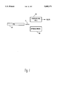
- FIG. 1 is a schematic illustration of thin tritiated porous silicon material in combination with a photovoltaic device and an optoelectronic device.
- the aspect ratio can be as much as 1 to 10 or even 1 to 100.
- curvature-induced effects due to the proximity to the pore tips
- quantum confinement due to the small sizes of the crystallites making up the pore tips
- quantum confinement due to the small sizes of the crystallites making up the pore walls
- depletion layers frequently found near semiconductor/electrolyte interfaces.
- Curvature-induced effects may arise from the fact that the pore surface in the region around the tip is necessarily nonplanar. In atomistic terms this necessitates a higher density of steps in the vicinity of that surface region. The increase in abundance of these surface line defects and their associated point defects such as kinks may in turn give rise to higher surface reactivity. However, these mechanism need not be mutually exclusive. They could be in effect concurrently, leading to the simultaneous evolution of more than one type of microstructural feature.
- the present invention exploits this fact by depositing tritium species onto those same interior pore surfaces via the same electrodissolution process that has been employed to synthesize porous silicon except for one key modification.
- the electrolyte is composed of a mixed hydrogen fluoride (HF)/tritiated fluoride (TF) solution.
- HF hydrogen fluoride
- TF tritiated fluoride
- the relative HF/TF composition determines the relative amount of tritium that is deposited as surface chemical species (e.g., as Si--H--T or Si--O--H) onto the interior pore surfaces in the porous silicon network.
- TPS tritiated porous silicon
- H e or H 2 a diluent
- This process depends on chemical vapor infiltration and exchange reaction between the tritium in the gas phase with the hydrogen present in the pore surfaces of PS.
- the amount of tritium deposited is controlled by the ratio of tritium present in the diluent gas. This is a vapor deposition method unlike that of the electrolytic route which depends on liquid phase processes.
- Both methods will deposit tritium onto the interior pore surfaces of the porous silicon resulting in a new material TPS.
- the chemisorbed species is desired for thermal stability of the device with the tritiated porous silicon (TPS) acting as the luminescent material.
- luminescence spectra is to be collected sing a spectrophotometer.
- a deuterated silicon photoluminescence (PL) data is ascertained in tritiated silicon radioluminescence (RL) measurements are made.
- PL deuterated silicon photoluminescence
- RL tritiated silicon radioluminescence
- the major difference lies in the nature of the excitation source.
- the excitation source is photons (i.e., light).
- RL the corresponding source is electrons.
- the optical measurements are closely similar aside from the nature of the excitation source.
- EL electroluminescence
- the free charge carriers such as electrons or holes
- These energetic charge carriers dissipate their energy in the host material via mainly electron-hole pair excitations and photon generations.
- An example is the commonly available LED (light emitting diode) in which a p-n junction type device is utilized under a forward bias that provides the external field.
- LED light emitting diode
- the cause has often been attributed to the difficulty of injecting carriers into the system. This can arise for a wide variety of reasons, such as high contact resistance. In fact the best EL performance from conventional porous silicon at present has been obtained by using liquid electrolyte contact.
- TPS wet contact is provided by immersing the PS layer in a liquid electrolyte which provides the medium for carrier injection.
- the carriers injected from the electrolyte would be the minority type (i.e., electrons).
- the electron emission source namely the tritium
- the range of the electrons implies that the carrier injection would not be an issue.
- TPS 10 can act as a stand alone power source emitting light 11. Its function is similar to other advanced stand-alone energy generating/storage devices such as batteries. However, unlike advanced batteries, which involve power levels in the range of KW to MW (particularly for utilities and transportation applications), the operating range of TPS is expected to be mWs or less. It is suited for the low-level power requirement characteristic of highly integrated devices in optoelectronics and control technology. Strictly speaking, TPS is not an energy storage device like a battery. Once in place TPS would generate light energy continuously. However, the very long time constant (11-12 years) allows TPS to operate as an energy generating source, while also effectively functioning like an energy storage device in the sense that power is available "on call" without the need for an external source of energy.
- TPS as a self-powered illumination source for low-level lighting applications where stand-alone and low or zero maintenance capabilities are of the highest priority.
- TPS photovoltaic cells 15 to generate electricity.
- the photovoltaic application involves the direct conversion of luminescent energy to electrical power.
- the lighting technology uses TPS as the illumination source.
- the optoelectronic application utilizes the optical output 11 from TPS 10 as a power supply and also as an interconnect between different electronic components 20.
- the common denominators to all these options are the stand-alone capability, the compactness of an inorganic solid state source, and the practically uninterruptable nature of its operating characteristics.
- TPS can be used as an on-board stand alone power supply for a silicon micromachine technology.
- micro-electro-mechanical systems are integrated devices called micro-electro-mechanical systems (MEMS). They may be composed of sensors, actuators, and/or electronic components all made out of silicon wafers using microfabrication techniques developed for the IC (integrated circuits) industry. Depending on their functions, these MEMS may range in size from a few microns to several hundred microns. Examples include micropumps, microvalves, and micro-acceleration sensors and related devices in a wide range of transportation, bio-medical, industrial process monitoring and control applications.
- MEMS micro-electro-mechanical systems
- TPS integrated circuit
- This combination can turn many current MEM's into self-powered smart (i.e. with problem-solving capability) micromachines, some of which may be optically transparent if the TPS is thin enough such as the few microns referred to above.
- PS porous silicon
- hydride species include SiH, SiH 2 and SiH 3 . It has been suggested that the dihydride may be the dominant one with a coverage on the order of 2.3 ⁇ 10 14 cm -2 .
- PS is a material that has a specific surface area as high as 900 m 2 cm -3 .
- TPS film of area 1 cm 2 and 10 microns in thickness is considered.
- This film contains 10 mCi of tritium; however, TPS having radiation in the range of from about 10 mCi to 100 mCi is preferred.
- Conventional gas tube-type tritium-based lighting technology has a typical conversion capacity of around 0.4 ft.-L per Ci.
- TPS should have significantly higher conversion capacity than in this example. This is due mainly to the much higher tritium concentration that can be achieved in TPS compared to the gas phase, as well as the total accessibility of the luminescent centers, to the emitted beta particles from the tritium. As a result, the conversion efficiency for TPS is estimated to be of the order of 34 ft.-L per Ci, substantially above that of the conventional technology.
- this thin film of TPS material (with a tritium content of about 10 mCi per c.c.) can generate initially 0.34 ft-L of light. For comparison an average TV monitor emits at a level of about 2 ft-L.
- TPS is useful for stand-alone low level lighting applications either directly as a light source or as an optical power source for optoelectronic devices.
- the tritium is in gaseous form contained in a gas tube whose surface is coated with phosphor-type materials. Due to the short mean free path of the emitted beta particles one cannot increase arbitrarily the output light intensity by increasing the tritium partial pressure and/or the diameter of the tube. This kind of approach is self-limiting by the self-absorption effect from the short mean free path.
- the typical tritium content utilized in gas-tube type of illumination devices is about half a curie, generating light at a level of around 0.2 ft.-L, which give a conversion efficiency of around 0.4 ft.-L. per Ci. Now the tritium concentration achievable in TPS can be easily an order of magnitude or more above that of the gas phase.
- TPS tritium concentration of about 10 Ci per cc.
- 0.5 atmosphere of tritium (which is the typical tritium content in conventional gas-tube devices) is equivalent to about 1.2 Ci per cc.
- TPS would have a conversion efficiency of 0.4 times (10/1.18) ft.-L. per Ci. This arises from the higher tritium density in TPS, an expected result for a solid-state device.
- the enhanced conversion efficiency of TPS would be a value on the order of 34 ft.-L. per Ci. This is substantially above what can be achieved with conventional devices.
- the fundamental reason is that in TPS one manages to pack more tritium into a greater amount of accessible luminescent materials than is possible with conventional gas-tube type technologies.
- E GAS is the conversion efficiency of gas-tube type tritium devices
- N TPS is the tritium density in TPS
- N GAS is the tritium density in the gas phase
- d TPS is the thickness of the TPS film
- SOLID is the range of the beta particles in solid state materials.
- tritium is a weakly emitting radionuclide for which the decay process is effected 100% through beta emission.
- One is the range of the beta particles in typical/window packaging materials that are likely candidates to be utilized to isolate the TPS from the external environment.
- the other issue is the dose on an individual due to failure of the window/packaging materials and the release of all the tritium into the air from the TPS-containing device.
- the range of a beta particle in a solid material is inversely proportional to its density. For most solid materials simple estimates give ranges that are under 1 micron. This means that a few microns thick window/packaging barrier is more than sufficient to stop the beta particles. Note that this is in addition to the presence of the porous silicon (PS) whose very purpose and configuration have already been designed to absorb as much of the beta emission as possible.
- PS porous silicon
- the above considerations apply to normal operation. Considering a situation in which for whatever reason there is a complete breakage of the window/packaging material barrier and all the tritium embedded in the pore surfaces of the TPS material is instantaneously released into the air (a truly immense event).
- the instantaneous total release of the tritium (using 10 mCi tritium content) is a worst case scenario.
- the tritium atoms are bonded to the pore surfaces in the form of surface chemisorbed species such as hydrides (e.g., SiHT) or as hydroxide.
- the actual release mechanism is likely to be through a combination of the slower processes of thermal desorption and exchange.
- the instantaneous total release assumption in the following estimate is used to provide a conservative boundary.
- the form of the released tritium is assumed to be the oxide form which represents the worst biohazard case. The likely scenario for this to happen is total oxidation of the tritium content in the TPS (e.g., as in a fire
Landscapes
- Engineering & Computer Science (AREA)
- Manufacturing & Machinery (AREA)
- Computer Hardware Design (AREA)
- Microelectronics & Electronic Packaging (AREA)
- Power Engineering (AREA)
- Luminescent Compositions (AREA)
Abstract
Description
E.sub.TPS =E.sub.GAS (N.sub.TPS /N.sub.GAS) d.sub.TPS /1.sup.SOLID)
Claims (23)
Priority Applications (3)
| Application Number | Priority Date | Filing Date | Title |
|---|---|---|---|
| US08/517,001 US5605171A (en) | 1995-08-18 | 1995-08-18 | Porous silicon with embedded tritium as a stand-alone prime power source for optoelectronic applications |
| US08/671,504 US5765680A (en) | 1995-08-18 | 1996-06-27 | Porous silicon with embedded tritium as a stand-alone prime power source for optoelectronic applications |
| US08/671,325 US5604162A (en) | 1995-08-18 | 1996-06-27 | Process of preparing tritiated porous silicon |
Applications Claiming Priority (1)
| Application Number | Priority Date | Filing Date | Title |
|---|---|---|---|
| US08/517,001 US5605171A (en) | 1995-08-18 | 1995-08-18 | Porous silicon with embedded tritium as a stand-alone prime power source for optoelectronic applications |
Related Child Applications (2)
| Application Number | Title | Priority Date | Filing Date |
|---|---|---|---|
| US08/671,325 Division US5604162A (en) | 1995-08-18 | 1996-06-27 | Process of preparing tritiated porous silicon |
| US08/671,504 Division US5765680A (en) | 1995-08-18 | 1996-06-27 | Porous silicon with embedded tritium as a stand-alone prime power source for optoelectronic applications |
Publications (1)
| Publication Number | Publication Date |
|---|---|
| US5605171A true US5605171A (en) | 1997-02-25 |
Family
ID=24057969
Family Applications (3)
| Application Number | Title | Priority Date | Filing Date |
|---|---|---|---|
| US08/517,001 Expired - Fee Related US5605171A (en) | 1995-08-18 | 1995-08-18 | Porous silicon with embedded tritium as a stand-alone prime power source for optoelectronic applications |
| US08/671,504 Expired - Fee Related US5765680A (en) | 1995-08-18 | 1996-06-27 | Porous silicon with embedded tritium as a stand-alone prime power source for optoelectronic applications |
| US08/671,325 Expired - Fee Related US5604162A (en) | 1995-08-18 | 1996-06-27 | Process of preparing tritiated porous silicon |
Family Applications After (2)
| Application Number | Title | Priority Date | Filing Date |
|---|---|---|---|
| US08/671,504 Expired - Fee Related US5765680A (en) | 1995-08-18 | 1996-06-27 | Porous silicon with embedded tritium as a stand-alone prime power source for optoelectronic applications |
| US08/671,325 Expired - Fee Related US5604162A (en) | 1995-08-18 | 1996-06-27 | Process of preparing tritiated porous silicon |
Country Status (1)
| Country | Link |
|---|---|
| US (3) | US5605171A (en) |
Cited By (19)
| Publication number | Priority date | Publication date | Assignee | Title |
|---|---|---|---|---|
| US5708957A (en) * | 1996-02-02 | 1998-01-13 | University Of Iowa Research Foundation | Optical sensor with radioluminescent light source |
| US6118204A (en) * | 1999-02-01 | 2000-09-12 | Brown; Paul M. | Layered metal foil semiconductor power device |
| US6232546B1 (en) | 1997-07-30 | 2001-05-15 | The Charles Stark Draper Laboratory, Inc. | Microcavity apparatus and systems for maintaining a microcavity over a macroscale area |
| US6238812B1 (en) | 1998-04-06 | 2001-05-29 | Paul M. Brown | Isotopic semiconductor batteries |
| US20040063650A1 (en) * | 2002-09-27 | 2004-04-01 | Sumitomo Chemical Company, Limited | Method for producing 3-methylthiopropanal |
| US20040150290A1 (en) * | 2003-01-31 | 2004-08-05 | Larry Gadeken | Apparatus and method for generating electrical current from the nuclear decay process of a radioactive material |
| US20040150229A1 (en) * | 2003-01-31 | 2004-08-05 | Larry Gadeken | Apparatus and method for generating electrical current from the nuclear decay process of a radioactive material |
| US20060185975A1 (en) * | 2005-02-22 | 2006-08-24 | Pentam, Inc. | Decomposition unit |
| US20060185723A1 (en) * | 2005-02-22 | 2006-08-24 | Pentam, Inc. | Method of manufacturing a nuclear-cored battery |
| US20060186378A1 (en) * | 2005-02-22 | 2006-08-24 | Pentam, Inc. | Crystalline of a nuclear-cored battery |
| US20060185719A1 (en) * | 2005-02-22 | 2006-08-24 | Pentam, Inc. | Nuclear-cored battery |
| US20060185724A1 (en) * | 2005-02-22 | 2006-08-24 | Pentam, Inc. | Super electromagnet |
| US20060185722A1 (en) * | 2005-02-22 | 2006-08-24 | Pentam, Inc. | Method of pre-selecting the life of a nuclear-cored product |
| US20060185153A1 (en) * | 2005-02-22 | 2006-08-24 | Pentam, Inc. | Method of making crystalline to surround a nuclear-core of a nuclear-cored battery |
| US20060185974A1 (en) * | 2005-02-22 | 2006-08-24 | Pentam, Inc. | Decomposition cell |
| US20060185721A1 (en) * | 2005-02-22 | 2006-08-24 | Pentam, Inc. | Layered nuclear-cored battery |
| US20060185720A1 (en) * | 2005-02-22 | 2006-08-24 | Pentam, Inc. | Method of recycling a nuclear-cored battery |
| US20120038243A1 (en) * | 2008-11-21 | 2012-02-16 | Trace Photonics, Inc. | High efficiency 4-pi negatron beta-3 particle emission source fabrication and its use as an electrode in a self-charged high-voltage capacitor |
| US8653715B1 (en) | 2011-06-30 | 2014-02-18 | The United States Of America As Represented By The Secretary Of The Navy | Radioisotope-powered energy source |
Families Citing this family (7)
| Publication number | Priority date | Publication date | Assignee | Title |
|---|---|---|---|---|
| US20020070635A1 (en) | 2000-10-13 | 2002-06-13 | Morrison Gerald O. | Self-powered wireless switch |
| US6700310B2 (en) | 2000-10-13 | 2004-03-02 | Lear Corporation | Self-powered wireless switch |
| FR2858313B1 (en) * | 2003-07-28 | 2005-12-16 | Centre Nat Rech Scient | HYDROGEN RESERVOIR BASED ON SILICON NANO STRUCTURES |
| US20060219956A1 (en) * | 2005-03-09 | 2006-10-05 | Bergman Joshua J | Device and method for generating characteristic radiation or energy |
| US20070238132A1 (en) * | 2006-04-04 | 2007-10-11 | Intematix Corporation | Screening of combinatorial libraries using radioactivity |
| US8492861B1 (en) | 2010-11-18 | 2013-07-23 | The United States Of America As Represented By The Secretary Of The Navy | Beta voltaic semiconductor diode fabricated from a radioisotope |
| US9018721B1 (en) | 2010-11-18 | 2015-04-28 | The United States Of America As Represented By The Secretary Of The Navy | Beta voltaic semiconductor photodiode fabricated from a radioisotope |
Citations (7)
| Publication number | Priority date | Publication date | Assignee | Title |
|---|---|---|---|---|
| US5082505A (en) * | 1988-12-29 | 1992-01-21 | Cota Albert O | Self-sustaining power module |
| US5124610A (en) * | 1989-03-03 | 1992-06-23 | E. F. Johnson Company | Tritiated light emitting polymer electrical energy source |
| US5272355A (en) * | 1992-05-20 | 1993-12-21 | Spire Corporation | Optoelectronic switching and display device with porous silicon |
| US5285078A (en) * | 1992-01-24 | 1994-02-08 | Nippon Steel Corporation | Light emitting element with employment of porous silicon and optical device utilizing light emitting element |
| US5301204A (en) * | 1992-09-15 | 1994-04-05 | Texas Instruments Incorporated | Porous silicon as a light source for rare earth-doped CaF2 laser |
| US5396141A (en) * | 1993-07-30 | 1995-03-07 | Texas Instruments Incorporated | Radioisotope power cells |
| US5443657A (en) * | 1993-09-16 | 1995-08-22 | Rivenburg; Howard C. | Power source using a photovoltaic array and self-luminous microspheres |
Family Cites Families (2)
| Publication number | Priority date | Publication date | Assignee | Title |
|---|---|---|---|---|
| US5137659A (en) * | 1990-03-20 | 1992-08-11 | The United States Of America As Represented By The United States Department Of Energy | Solid-state radiation-emitting compositions and devices |
| US5122305A (en) * | 1990-03-20 | 1992-06-16 | Ashley Carol S | Solid-state radiation-emitting compositions and devices |
-
1995
- 1995-08-18 US US08/517,001 patent/US5605171A/en not_active Expired - Fee Related
-
1996
- 1996-06-27 US US08/671,504 patent/US5765680A/en not_active Expired - Fee Related
- 1996-06-27 US US08/671,325 patent/US5604162A/en not_active Expired - Fee Related
Patent Citations (7)
| Publication number | Priority date | Publication date | Assignee | Title |
|---|---|---|---|---|
| US5082505A (en) * | 1988-12-29 | 1992-01-21 | Cota Albert O | Self-sustaining power module |
| US5124610A (en) * | 1989-03-03 | 1992-06-23 | E. F. Johnson Company | Tritiated light emitting polymer electrical energy source |
| US5285078A (en) * | 1992-01-24 | 1994-02-08 | Nippon Steel Corporation | Light emitting element with employment of porous silicon and optical device utilizing light emitting element |
| US5272355A (en) * | 1992-05-20 | 1993-12-21 | Spire Corporation | Optoelectronic switching and display device with porous silicon |
| US5301204A (en) * | 1992-09-15 | 1994-04-05 | Texas Instruments Incorporated | Porous silicon as a light source for rare earth-doped CaF2 laser |
| US5396141A (en) * | 1993-07-30 | 1995-03-07 | Texas Instruments Incorporated | Radioisotope power cells |
| US5443657A (en) * | 1993-09-16 | 1995-08-22 | Rivenburg; Howard C. | Power source using a photovoltaic array and self-luminous microspheres |
Cited By (28)
| Publication number | Priority date | Publication date | Assignee | Title |
|---|---|---|---|---|
| US5708957A (en) * | 1996-02-02 | 1998-01-13 | University Of Iowa Research Foundation | Optical sensor with radioluminescent light source |
| US6232546B1 (en) | 1997-07-30 | 2001-05-15 | The Charles Stark Draper Laboratory, Inc. | Microcavity apparatus and systems for maintaining a microcavity over a macroscale area |
| US6238812B1 (en) | 1998-04-06 | 2001-05-29 | Paul M. Brown | Isotopic semiconductor batteries |
| US6118204A (en) * | 1999-02-01 | 2000-09-12 | Brown; Paul M. | Layered metal foil semiconductor power device |
| US20040063650A1 (en) * | 2002-09-27 | 2004-04-01 | Sumitomo Chemical Company, Limited | Method for producing 3-methylthiopropanal |
| US7799953B2 (en) * | 2002-09-27 | 2010-09-21 | Sumitomo Chemical Company, Limited | Method for producing 3-methylthiopropanal |
| US20040150290A1 (en) * | 2003-01-31 | 2004-08-05 | Larry Gadeken | Apparatus and method for generating electrical current from the nuclear decay process of a radioactive material |
| US20040150229A1 (en) * | 2003-01-31 | 2004-08-05 | Larry Gadeken | Apparatus and method for generating electrical current from the nuclear decay process of a radioactive material |
| US6774531B1 (en) | 2003-01-31 | 2004-08-10 | Betabatt, Inc. | Apparatus and method for generating electrical current from the nuclear decay process of a radioactive material |
| US6949865B2 (en) | 2003-01-31 | 2005-09-27 | Betabatt, Inc. | Apparatus and method for generating electrical current from the nuclear decay process of a radioactive material |
| US20060185722A1 (en) * | 2005-02-22 | 2006-08-24 | Pentam, Inc. | Method of pre-selecting the life of a nuclear-cored product |
| US7438789B2 (en) | 2005-02-22 | 2008-10-21 | Medusa Special Projects, Llc | Decomposition cell |
| US20060185719A1 (en) * | 2005-02-22 | 2006-08-24 | Pentam, Inc. | Nuclear-cored battery |
| US20060185724A1 (en) * | 2005-02-22 | 2006-08-24 | Pentam, Inc. | Super electromagnet |
| US20060185723A1 (en) * | 2005-02-22 | 2006-08-24 | Pentam, Inc. | Method of manufacturing a nuclear-cored battery |
| US20060185153A1 (en) * | 2005-02-22 | 2006-08-24 | Pentam, Inc. | Method of making crystalline to surround a nuclear-core of a nuclear-cored battery |
| US20060185974A1 (en) * | 2005-02-22 | 2006-08-24 | Pentam, Inc. | Decomposition cell |
| US20060185721A1 (en) * | 2005-02-22 | 2006-08-24 | Pentam, Inc. | Layered nuclear-cored battery |
| US20060185720A1 (en) * | 2005-02-22 | 2006-08-24 | Pentam, Inc. | Method of recycling a nuclear-cored battery |
| US20060186378A1 (en) * | 2005-02-22 | 2006-08-24 | Pentam, Inc. | Crystalline of a nuclear-cored battery |
| US7482533B2 (en) | 2005-02-22 | 2009-01-27 | Medusa Special Projects, Llc | Nuclear-cored battery |
| US7488889B2 (en) | 2005-02-22 | 2009-02-10 | Medusa Special Projects, Llc | Layered nuclear-cored battery |
| US7491881B2 (en) | 2005-02-22 | 2009-02-17 | Medusa Special Projects, Llc | Method of manufacturing a nuclear-cored battery |
| US7491882B2 (en) | 2005-02-22 | 2009-02-17 | Medusa Special Projects, Llc | Super electromagnet |
| US20060185975A1 (en) * | 2005-02-22 | 2006-08-24 | Pentam, Inc. | Decomposition unit |
| US20120038243A1 (en) * | 2008-11-21 | 2012-02-16 | Trace Photonics, Inc. | High efficiency 4-pi negatron beta-3 particle emission source fabrication and its use as an electrode in a self-charged high-voltage capacitor |
| US8134275B2 (en) * | 2008-11-21 | 2012-03-13 | Trace Photonics, Inc. | High efficiency 4-π negatron β-3 particle emission source fabrication and its use as an electrode in a self-charged high-voltage capacitor |
| US8653715B1 (en) | 2011-06-30 | 2014-02-18 | The United States Of America As Represented By The Secretary Of The Navy | Radioisotope-powered energy source |
Also Published As
| Publication number | Publication date |
|---|---|
| US5765680A (en) | 1998-06-16 |
| US5604162A (en) | 1997-02-18 |
Similar Documents
| Publication | Publication Date | Title |
|---|---|---|
| US5605171A (en) | Porous silicon with embedded tritium as a stand-alone prime power source for optoelectronic applications | |
| US7867639B2 (en) | Alpha voltaic batteries and methods thereof | |
| US5443657A (en) | Power source using a photovoltaic array and self-luminous microspheres | |
| US5124610A (en) | Tritiated light emitting polymer electrical energy source | |
| CA1301838C (en) | Self-sustaining power module | |
| US5396141A (en) | Radioisotope power cells | |
| White | Scintillating fibres | |
| PT93327B (en) | ELECTRICAL ENERGY SOURCE INCLUDING A LIGHTING POLYMER | |
| JP4769254B2 (en) | Organic electroluminescent light source | |
| JP2007509345A (en) | Neutron detection device and manufacturing method thereof | |
| CN103996733A (en) | Photoelectric nuclear battery | |
| Hong et al. | Parameter optimization and experiment verification for a beta radioluminescence nuclear battery | |
| KR100926598B1 (en) | Atomic cell | |
| US11875908B2 (en) | Electrode with radioisotope and phosphor composite layer for hybrid radioisotope batteries and radioluminescent surfaces | |
| Russo et al. | Demonstration of a tritiated nitroxide nuclear battery | |
| JP2002510035A (en) | Methods and devices for semiconductor electric generators using radionuclide induced exciton products | |
| Lee et al. | Development of nuclear micro-battery with solid tritium source | |
| CN106997788A (en) | A kind of GaAs photovoltaic isotope battery | |
| CN105070341A (en) | Preparation method of photoelectric nuclear battery | |
| WO2000022629A1 (en) | Power cell | |
| Kavetsky et al. | Conversion of radioactive decay energy to electricity | |
| Weaver III | PIDECα: photon intermediate direct energy conversion using the alpha emitter polonium-210 | |
| Walko et al. | Electronic and photonic power applications | |
| Prelas et al. | Wide band-gap photovoltaics | |
| CN218602444U (en) | Photovoltaic module with night illumination function |
Legal Events
| Date | Code | Title | Description |
|---|---|---|---|
| AS | Assignment |
Owner name: CHICAGO, UNIVERSITY OF, ILLINOIS Free format text: ASSIGNMENT OF ASSIGNORS INTEREST;ASSIGNOR:TAM, SHIU WING;REEL/FRAME:007624/0744 Effective date: 19950802 |
|
| AS | Assignment |
Owner name: ENERGY, DEPARTMENT OF, UNITED STATES, DISTRICT OF Free format text: CONFIRMATORY LICENSE;ASSIGNOR:CHICAGO, UNIVERSITY OF;REEL/FRAME:008034/0001 Effective date: 19951010 |
|
| FPAY | Fee payment |
Year of fee payment: 4 |
|
| FEPP | Fee payment procedure |
Free format text: PAYOR NUMBER ASSIGNED (ORIGINAL EVENT CODE: ASPN); ENTITY STATUS OF PATENT OWNER: SMALL ENTITY |
|
| FPAY | Fee payment |
Year of fee payment: 8 |
|
| AS | Assignment |
Owner name: U CHICAGO ARGONNE LLC,ILLINOIS Free format text: ASSIGNMENT OF ASSIGNORS INTEREST;ASSIGNOR:UNIVERSITY OF CHICAGO, THE;REEL/FRAME:018385/0618 Effective date: 20060925 Owner name: U CHICAGO ARGONNE LLC, ILLINOIS Free format text: ASSIGNMENT OF ASSIGNORS INTEREST;ASSIGNOR:UNIVERSITY OF CHICAGO, THE;REEL/FRAME:018385/0618 Effective date: 20060925 |
|
| REMI | Maintenance fee reminder mailed | ||
| LAPS | Lapse for failure to pay maintenance fees | ||
| STCH | Information on status: patent discontinuation |
Free format text: PATENT EXPIRED DUE TO NONPAYMENT OF MAINTENANCE FEES UNDER 37 CFR 1.362 |
|
| FP | Lapsed due to failure to pay maintenance fee |
Effective date: 20090225 |