US5620928A - Ultra thin ball grid array using a flex tape or printed wiring board substrate and method - Google Patents
Ultra thin ball grid array using a flex tape or printed wiring board substrate and method Download PDFInfo
- Publication number
- US5620928A US5620928A US08/439,362 US43936295A US5620928A US 5620928 A US5620928 A US 5620928A US 43936295 A US43936295 A US 43936295A US 5620928 A US5620928 A US 5620928A
- Authority
- US
- United States
- Prior art keywords
- substrate
- integrated circuit
- dielectric
- circuit die
- top surface
- Prior art date
- Legal status (The legal status is an assumption and is not a legal conclusion. Google has not performed a legal analysis and makes no representation as to the accuracy of the status listed.)
- Expired - Lifetime
Links
Images


Classifications
-
- H—ELECTRICITY
- H01—ELECTRIC ELEMENTS
- H01L—SEMICONDUCTOR DEVICES NOT COVERED BY CLASS H10
- H01L24/00—Arrangements for connecting or disconnecting semiconductor or solid-state bodies; Methods or apparatus related thereto
- H01L24/73—Means for bonding being of different types provided for in two or more of groups H01L24/10, H01L24/18, H01L24/26, H01L24/34, H01L24/42, H01L24/50, H01L24/63, H01L24/71
-
- H—ELECTRICITY
- H01—ELECTRIC ELEMENTS
- H01L—SEMICONDUCTOR DEVICES NOT COVERED BY CLASS H10
- H01L23/00—Details of semiconductor or other solid state devices
- H01L23/28—Encapsulations, e.g. encapsulating layers, coatings, e.g. for protection
-
- H—ELECTRICITY
- H01—ELECTRIC ELEMENTS
- H01L—SEMICONDUCTOR DEVICES NOT COVERED BY CLASS H10
- H01L23/00—Details of semiconductor or other solid state devices
- H01L23/12—Mountings, e.g. non-detachable insulating substrates
- H01L23/13—Mountings, e.g. non-detachable insulating substrates characterised by the shape
-
- H—ELECTRICITY
- H01—ELECTRIC ELEMENTS
- H01L—SEMICONDUCTOR DEVICES NOT COVERED BY CLASS H10
- H01L23/00—Details of semiconductor or other solid state devices
- H01L23/28—Encapsulations, e.g. encapsulating layers, coatings, e.g. for protection
- H01L23/31—Encapsulations, e.g. encapsulating layers, coatings, e.g. for protection characterised by the arrangement or shape
- H01L23/3107—Encapsulations, e.g. encapsulating layers, coatings, e.g. for protection characterised by the arrangement or shape the device being completely enclosed
- H01L23/3121—Encapsulations, e.g. encapsulating layers, coatings, e.g. for protection characterised by the arrangement or shape the device being completely enclosed a substrate forming part of the encapsulation
- H01L23/3128—Encapsulations, e.g. encapsulating layers, coatings, e.g. for protection characterised by the arrangement or shape the device being completely enclosed a substrate forming part of the encapsulation the substrate having spherical bumps for external connection
-
- H—ELECTRICITY
- H01—ELECTRIC ELEMENTS
- H01L—SEMICONDUCTOR DEVICES NOT COVERED BY CLASS H10
- H01L23/00—Details of semiconductor or other solid state devices
- H01L23/48—Arrangements for conducting electric current to or from the solid state body in operation, e.g. leads, terminal arrangements ; Selection of materials therefor
- H01L23/488—Arrangements for conducting electric current to or from the solid state body in operation, e.g. leads, terminal arrangements ; Selection of materials therefor consisting of soldered or bonded constructions
- H01L23/498—Leads, i.e. metallisations or lead-frames on insulating substrates, e.g. chip carriers
- H01L23/4985—Flexible insulating substrates
-
- H—ELECTRICITY
- H01—ELECTRIC ELEMENTS
- H01L—SEMICONDUCTOR DEVICES NOT COVERED BY CLASS H10
- H01L2224/00—Indexing scheme for arrangements for connecting or disconnecting semiconductor or solid-state bodies and methods related thereto as covered by H01L24/00
- H01L2224/01—Means for bonding being attached to, or being formed on, the surface to be connected, e.g. chip-to-package, die-attach, "first-level" interconnects; Manufacturing methods related thereto
- H01L2224/02—Bonding areas; Manufacturing methods related thereto
- H01L2224/04—Structure, shape, material or disposition of the bonding areas prior to the connecting process
- H01L2224/05—Structure, shape, material or disposition of the bonding areas prior to the connecting process of an individual bonding area
- H01L2224/0554—External layer
- H01L2224/0555—Shape
- H01L2224/05552—Shape in top view
- H01L2224/05554—Shape in top view being square
-
- H—ELECTRICITY
- H01—ELECTRIC ELEMENTS
- H01L—SEMICONDUCTOR DEVICES NOT COVERED BY CLASS H10
- H01L2224/00—Indexing scheme for arrangements for connecting or disconnecting semiconductor or solid-state bodies and methods related thereto as covered by H01L24/00
- H01L2224/01—Means for bonding being attached to, or being formed on, the surface to be connected, e.g. chip-to-package, die-attach, "first-level" interconnects; Manufacturing methods related thereto
- H01L2224/10—Bump connectors; Manufacturing methods related thereto
- H01L2224/15—Structure, shape, material or disposition of the bump connectors after the connecting process
- H01L2224/16—Structure, shape, material or disposition of the bump connectors after the connecting process of an individual bump connector
- H01L2224/161—Disposition
- H01L2224/16151—Disposition the bump connector connecting between a semiconductor or solid-state body and an item not being a semiconductor or solid-state body, e.g. chip-to-substrate, chip-to-passive
- H01L2224/16221—Disposition the bump connector connecting between a semiconductor or solid-state body and an item not being a semiconductor or solid-state body, e.g. chip-to-substrate, chip-to-passive the body and the item being stacked
- H01L2224/16225—Disposition the bump connector connecting between a semiconductor or solid-state body and an item not being a semiconductor or solid-state body, e.g. chip-to-substrate, chip-to-passive the body and the item being stacked the item being non-metallic, e.g. insulating substrate with or without metallisation
-
- H—ELECTRICITY
- H01—ELECTRIC ELEMENTS
- H01L—SEMICONDUCTOR DEVICES NOT COVERED BY CLASS H10
- H01L2224/00—Indexing scheme for arrangements for connecting or disconnecting semiconductor or solid-state bodies and methods related thereto as covered by H01L24/00
- H01L2224/01—Means for bonding being attached to, or being formed on, the surface to be connected, e.g. chip-to-package, die-attach, "first-level" interconnects; Manufacturing methods related thereto
- H01L2224/26—Layer connectors, e.g. plate connectors, solder or adhesive layers; Manufacturing methods related thereto
- H01L2224/31—Structure, shape, material or disposition of the layer connectors after the connecting process
- H01L2224/32—Structure, shape, material or disposition of the layer connectors after the connecting process of an individual layer connector
- H01L2224/321—Disposition
- H01L2224/32151—Disposition the layer connector connecting between a semiconductor or solid-state body and an item not being a semiconductor or solid-state body, e.g. chip-to-substrate, chip-to-passive
- H01L2224/32221—Disposition the layer connector connecting between a semiconductor or solid-state body and an item not being a semiconductor or solid-state body, e.g. chip-to-substrate, chip-to-passive the body and the item being stacked
- H01L2224/32225—Disposition the layer connector connecting between a semiconductor or solid-state body and an item not being a semiconductor or solid-state body, e.g. chip-to-substrate, chip-to-passive the body and the item being stacked the item being non-metallic, e.g. insulating substrate with or without metallisation
-
- H—ELECTRICITY
- H01—ELECTRIC ELEMENTS
- H01L—SEMICONDUCTOR DEVICES NOT COVERED BY CLASS H10
- H01L2224/00—Indexing scheme for arrangements for connecting or disconnecting semiconductor or solid-state bodies and methods related thereto as covered by H01L24/00
- H01L2224/01—Means for bonding being attached to, or being formed on, the surface to be connected, e.g. chip-to-package, die-attach, "first-level" interconnects; Manufacturing methods related thereto
- H01L2224/42—Wire connectors; Manufacturing methods related thereto
- H01L2224/47—Structure, shape, material or disposition of the wire connectors after the connecting process
- H01L2224/48—Structure, shape, material or disposition of the wire connectors after the connecting process of an individual wire connector
- H01L2224/4805—Shape
- H01L2224/4809—Loop shape
- H01L2224/48091—Arched
-
- H—ELECTRICITY
- H01—ELECTRIC ELEMENTS
- H01L—SEMICONDUCTOR DEVICES NOT COVERED BY CLASS H10
- H01L2224/00—Indexing scheme for arrangements for connecting or disconnecting semiconductor or solid-state bodies and methods related thereto as covered by H01L24/00
- H01L2224/01—Means for bonding being attached to, or being formed on, the surface to be connected, e.g. chip-to-package, die-attach, "first-level" interconnects; Manufacturing methods related thereto
- H01L2224/42—Wire connectors; Manufacturing methods related thereto
- H01L2224/47—Structure, shape, material or disposition of the wire connectors after the connecting process
- H01L2224/48—Structure, shape, material or disposition of the wire connectors after the connecting process of an individual wire connector
- H01L2224/481—Disposition
- H01L2224/48151—Connecting between a semiconductor or solid-state body and an item not being a semiconductor or solid-state body, e.g. chip-to-substrate, chip-to-passive
- H01L2224/48221—Connecting between a semiconductor or solid-state body and an item not being a semiconductor or solid-state body, e.g. chip-to-substrate, chip-to-passive the body and the item being stacked
- H01L2224/48225—Connecting between a semiconductor or solid-state body and an item not being a semiconductor or solid-state body, e.g. chip-to-substrate, chip-to-passive the body and the item being stacked the item being non-metallic, e.g. insulating substrate with or without metallisation
- H01L2224/48227—Connecting between a semiconductor or solid-state body and an item not being a semiconductor or solid-state body, e.g. chip-to-substrate, chip-to-passive the body and the item being stacked the item being non-metallic, e.g. insulating substrate with or without metallisation connecting the wire to a bond pad of the item
-
- H—ELECTRICITY
- H01—ELECTRIC ELEMENTS
- H01L—SEMICONDUCTOR DEVICES NOT COVERED BY CLASS H10
- H01L2224/00—Indexing scheme for arrangements for connecting or disconnecting semiconductor or solid-state bodies and methods related thereto as covered by H01L24/00
- H01L2224/01—Means for bonding being attached to, or being formed on, the surface to be connected, e.g. chip-to-package, die-attach, "first-level" interconnects; Manufacturing methods related thereto
- H01L2224/42—Wire connectors; Manufacturing methods related thereto
- H01L2224/47—Structure, shape, material or disposition of the wire connectors after the connecting process
- H01L2224/48—Structure, shape, material or disposition of the wire connectors after the connecting process of an individual wire connector
- H01L2224/484—Connecting portions
- H01L2224/48463—Connecting portions the connecting portion on the bonding area of the semiconductor or solid-state body being a ball bond
- H01L2224/48465—Connecting portions the connecting portion on the bonding area of the semiconductor or solid-state body being a ball bond the other connecting portion not on the bonding area being a wedge bond, i.e. ball-to-wedge, regular stitch
-
- H—ELECTRICITY
- H01—ELECTRIC ELEMENTS
- H01L—SEMICONDUCTOR DEVICES NOT COVERED BY CLASS H10
- H01L2224/00—Indexing scheme for arrangements for connecting or disconnecting semiconductor or solid-state bodies and methods related thereto as covered by H01L24/00
- H01L2224/01—Means for bonding being attached to, or being formed on, the surface to be connected, e.g. chip-to-package, die-attach, "first-level" interconnects; Manufacturing methods related thereto
- H01L2224/42—Wire connectors; Manufacturing methods related thereto
- H01L2224/47—Structure, shape, material or disposition of the wire connectors after the connecting process
- H01L2224/49—Structure, shape, material or disposition of the wire connectors after the connecting process of a plurality of wire connectors
- H01L2224/491—Disposition
- H01L2224/49105—Connecting at different heights
- H01L2224/49109—Connecting at different heights outside the semiconductor or solid-state body
-
- H—ELECTRICITY
- H01—ELECTRIC ELEMENTS
- H01L—SEMICONDUCTOR DEVICES NOT COVERED BY CLASS H10
- H01L2224/00—Indexing scheme for arrangements for connecting or disconnecting semiconductor or solid-state bodies and methods related thereto as covered by H01L24/00
- H01L2224/01—Means for bonding being attached to, or being formed on, the surface to be connected, e.g. chip-to-package, die-attach, "first-level" interconnects; Manufacturing methods related thereto
- H01L2224/42—Wire connectors; Manufacturing methods related thereto
- H01L2224/47—Structure, shape, material or disposition of the wire connectors after the connecting process
- H01L2224/49—Structure, shape, material or disposition of the wire connectors after the connecting process of a plurality of wire connectors
- H01L2224/491—Disposition
- H01L2224/4912—Layout
- H01L2224/49171—Fan-out arrangements
-
- H—ELECTRICITY
- H01—ELECTRIC ELEMENTS
- H01L—SEMICONDUCTOR DEVICES NOT COVERED BY CLASS H10
- H01L2224/00—Indexing scheme for arrangements for connecting or disconnecting semiconductor or solid-state bodies and methods related thereto as covered by H01L24/00
- H01L2224/73—Means for bonding being of different types provided for in two or more of groups H01L2224/10, H01L2224/18, H01L2224/26, H01L2224/34, H01L2224/42, H01L2224/50, H01L2224/63, H01L2224/71
- H01L2224/732—Location after the connecting process
- H01L2224/73251—Location after the connecting process on different surfaces
- H01L2224/73257—Bump and wire connectors
-
- H—ELECTRICITY
- H01—ELECTRIC ELEMENTS
- H01L—SEMICONDUCTOR DEVICES NOT COVERED BY CLASS H10
- H01L2224/00—Indexing scheme for arrangements for connecting or disconnecting semiconductor or solid-state bodies and methods related thereto as covered by H01L24/00
- H01L2224/73—Means for bonding being of different types provided for in two or more of groups H01L2224/10, H01L2224/18, H01L2224/26, H01L2224/34, H01L2224/42, H01L2224/50, H01L2224/63, H01L2224/71
- H01L2224/732—Location after the connecting process
- H01L2224/73251—Location after the connecting process on different surfaces
- H01L2224/73265—Layer and wire connectors
-
- H—ELECTRICITY
- H01—ELECTRIC ELEMENTS
- H01L—SEMICONDUCTOR DEVICES NOT COVERED BY CLASS H10
- H01L24/00—Arrangements for connecting or disconnecting semiconductor or solid-state bodies; Methods or apparatus related thereto
- H01L24/01—Means for bonding being attached to, or being formed on, the surface to be connected, e.g. chip-to-package, die-attach, "first-level" interconnects; Manufacturing methods related thereto
- H01L24/42—Wire connectors; Manufacturing methods related thereto
- H01L24/47—Structure, shape, material or disposition of the wire connectors after the connecting process
- H01L24/48—Structure, shape, material or disposition of the wire connectors after the connecting process of an individual wire connector
-
- H—ELECTRICITY
- H01—ELECTRIC ELEMENTS
- H01L—SEMICONDUCTOR DEVICES NOT COVERED BY CLASS H10
- H01L24/00—Arrangements for connecting or disconnecting semiconductor or solid-state bodies; Methods or apparatus related thereto
- H01L24/01—Means for bonding being attached to, or being formed on, the surface to be connected, e.g. chip-to-package, die-attach, "first-level" interconnects; Manufacturing methods related thereto
- H01L24/42—Wire connectors; Manufacturing methods related thereto
- H01L24/47—Structure, shape, material or disposition of the wire connectors after the connecting process
- H01L24/49—Structure, shape, material or disposition of the wire connectors after the connecting process of a plurality of wire connectors
-
- H—ELECTRICITY
- H01—ELECTRIC ELEMENTS
- H01L—SEMICONDUCTOR DEVICES NOT COVERED BY CLASS H10
- H01L2924/00—Indexing scheme for arrangements or methods for connecting or disconnecting semiconductor or solid-state bodies as covered by H01L24/00
- H01L2924/0001—Technical content checked by a classifier
- H01L2924/00014—Technical content checked by a classifier the subject-matter covered by the group, the symbol of which is combined with the symbol of this group, being disclosed without further technical details
-
- H—ELECTRICITY
- H01—ELECTRIC ELEMENTS
- H01L—SEMICONDUCTOR DEVICES NOT COVERED BY CLASS H10
- H01L2924/00—Indexing scheme for arrangements or methods for connecting or disconnecting semiconductor or solid-state bodies as covered by H01L24/00
- H01L2924/01—Chemical elements
- H01L2924/01005—Boron [B]
-
- H—ELECTRICITY
- H01—ELECTRIC ELEMENTS
- H01L—SEMICONDUCTOR DEVICES NOT COVERED BY CLASS H10
- H01L2924/00—Indexing scheme for arrangements or methods for connecting or disconnecting semiconductor or solid-state bodies as covered by H01L24/00
- H01L2924/01—Chemical elements
- H01L2924/01006—Carbon [C]
-
- H—ELECTRICITY
- H01—ELECTRIC ELEMENTS
- H01L—SEMICONDUCTOR DEVICES NOT COVERED BY CLASS H10
- H01L2924/00—Indexing scheme for arrangements or methods for connecting or disconnecting semiconductor or solid-state bodies as covered by H01L24/00
- H01L2924/01—Chemical elements
- H01L2924/01033—Arsenic [As]
-
- H—ELECTRICITY
- H01—ELECTRIC ELEMENTS
- H01L—SEMICONDUCTOR DEVICES NOT COVERED BY CLASS H10
- H01L2924/00—Indexing scheme for arrangements or methods for connecting or disconnecting semiconductor or solid-state bodies as covered by H01L24/00
- H01L2924/10—Details of semiconductor or other solid state devices to be connected
- H01L2924/1015—Shape
- H01L2924/1016—Shape being a cuboid
- H01L2924/10162—Shape being a cuboid with a square active surface
-
- H—ELECTRICITY
- H01—ELECTRIC ELEMENTS
- H01L—SEMICONDUCTOR DEVICES NOT COVERED BY CLASS H10
- H01L2924/00—Indexing scheme for arrangements or methods for connecting or disconnecting semiconductor or solid-state bodies as covered by H01L24/00
- H01L2924/10—Details of semiconductor or other solid state devices to be connected
- H01L2924/11—Device type
- H01L2924/14—Integrated circuits
-
- H—ELECTRICITY
- H01—ELECTRIC ELEMENTS
- H01L—SEMICONDUCTOR DEVICES NOT COVERED BY CLASS H10
- H01L2924/00—Indexing scheme for arrangements or methods for connecting or disconnecting semiconductor or solid-state bodies as covered by H01L24/00
- H01L2924/15—Details of package parts other than the semiconductor or other solid state devices to be connected
- H01L2924/151—Die mounting substrate
- H01L2924/1515—Shape
- H01L2924/15153—Shape the die mounting substrate comprising a recess for hosting the device
-
- H—ELECTRICITY
- H01—ELECTRIC ELEMENTS
- H01L—SEMICONDUCTOR DEVICES NOT COVERED BY CLASS H10
- H01L2924/00—Indexing scheme for arrangements or methods for connecting or disconnecting semiconductor or solid-state bodies as covered by H01L24/00
- H01L2924/15—Details of package parts other than the semiconductor or other solid state devices to be connected
- H01L2924/151—Die mounting substrate
- H01L2924/1517—Multilayer substrate
- H01L2924/15172—Fan-out arrangement of the internal vias
- H01L2924/15173—Fan-out arrangement of the internal vias in a single layer of the multilayer substrate
-
- H—ELECTRICITY
- H01—ELECTRIC ELEMENTS
- H01L—SEMICONDUCTOR DEVICES NOT COVERED BY CLASS H10
- H01L2924/00—Indexing scheme for arrangements or methods for connecting or disconnecting semiconductor or solid-state bodies as covered by H01L24/00
- H01L2924/15—Details of package parts other than the semiconductor or other solid state devices to be connected
- H01L2924/151—Die mounting substrate
- H01L2924/153—Connection portion
- H01L2924/1531—Connection portion the connection portion being formed only on the surface of the substrate opposite to the die mounting surface
- H01L2924/15311—Connection portion the connection portion being formed only on the surface of the substrate opposite to the die mounting surface being a ball array, e.g. BGA
-
- H—ELECTRICITY
- H01—ELECTRIC ELEMENTS
- H01L—SEMICONDUCTOR DEVICES NOT COVERED BY CLASS H10
- H01L2924/00—Indexing scheme for arrangements or methods for connecting or disconnecting semiconductor or solid-state bodies as covered by H01L24/00
- H01L2924/15—Details of package parts other than the semiconductor or other solid state devices to be connected
- H01L2924/181—Encapsulation
- H01L2924/1815—Shape
- H01L2924/1816—Exposing the passive side of the semiconductor or solid-state body
- H01L2924/18165—Exposing the passive side of the semiconductor or solid-state body of a wire bonded chip
-
- Y—GENERAL TAGGING OF NEW TECHNOLOGICAL DEVELOPMENTS; GENERAL TAGGING OF CROSS-SECTIONAL TECHNOLOGIES SPANNING OVER SEVERAL SECTIONS OF THE IPC; TECHNICAL SUBJECTS COVERED BY FORMER USPC CROSS-REFERENCE ART COLLECTIONS [XRACs] AND DIGESTS
- Y10—TECHNICAL SUBJECTS COVERED BY FORMER USPC
- Y10T—TECHNICAL SUBJECTS COVERED BY FORMER US CLASSIFICATION
- Y10T29/00—Metal working
- Y10T29/49—Method of mechanical manufacture
- Y10T29/49002—Electrical device making
- Y10T29/49117—Conductor or circuit manufacturing
- Y10T29/49124—On flat or curved insulated base, e.g., printed circuit, etc.
- Y10T29/4913—Assembling to base an electrical component, e.g., capacitor, etc.
- Y10T29/49146—Assembling to base an electrical component, e.g., capacitor, etc. with encapsulating, e.g., potting, etc.
-
- Y—GENERAL TAGGING OF NEW TECHNOLOGICAL DEVELOPMENTS; GENERAL TAGGING OF CROSS-SECTIONAL TECHNOLOGIES SPANNING OVER SEVERAL SECTIONS OF THE IPC; TECHNICAL SUBJECTS COVERED BY FORMER USPC CROSS-REFERENCE ART COLLECTIONS [XRACs] AND DIGESTS
- Y10—TECHNICAL SUBJECTS COVERED BY FORMER USPC
- Y10T—TECHNICAL SUBJECTS COVERED BY FORMER US CLASSIFICATION
- Y10T29/00—Metal working
- Y10T29/49—Method of mechanical manufacture
- Y10T29/49002—Electrical device making
- Y10T29/49117—Conductor or circuit manufacturing
- Y10T29/49169—Assembling electrical component directly to terminal or elongated conductor
- Y10T29/49171—Assembling electrical component directly to terminal or elongated conductor with encapsulating
Definitions
- the present invention relates generally to integrated circuit packaging and more specifically to an Ultra Thin Ball Grid Array (UTBGA) integrated circuit package and a method of making the package which uses a temporary supporting substrate carrier to support the components of the package during the assembly of the package.
- UMBGA Ultra Thin Ball Grid Array
- Prior an Ball Grid Array (BGA) packages There are currently several types of prior an Ball Grid Array (BGA) packages currently available. These prior an types include the Plastic Ball Grid Array (PBGA), the Ceramic Ball Grid Array (CBGA), and the Tape Ball Grid Array (TBGA).
- PBGA Plastic Ball Grid Array
- CBGA Ceramic Ball Grid Array
- TBGA Tape Ball Grid Array
- the PBGA and the TBGA are the thinnest ball grid array packages currently available.
- Prior art package 10 includes a dielectric substrate 12 an integrated circuit die 14, an array of bonding wires 16, an encapsulating material 18, and an array of contacts or solder balls 20.
- substrate 12 has a top surface 22, a bottom surface 24, a plurality of electrically conductive terminal pads 26 on the top surface 22 of substrate 12, a plurality of contact terminal pads 28 on the bottom surface 24 of substrate 12, and a plurality of electrically conductive traces (not shown). Each of the electrically conductive traces interconnects a respective one of terminal pads 26 on the top of substrate 12 to an associated contact terminal pad 28 on the bottom of substrate 12.
- Substrate 12 is made from a rigid material capable of supporting the other components of the package during the assembly of the package.
- Integrated circuit die 14 has a top surface 30, a bottom surface 32, and includes a plurality of input/output terminals 34 on its top surface 30.
- Each of the bonding wires 16 electrically connect a respective one of terminal pads 34 to an associated terminal pad 26 on the top surface of substrate 12.
- Encapsulating material 18 encapsulates integrated circuit die 14, at least the top surface of substrate 12, and bonding wires 16.
- Contacts or solder balls 20 are attached to associated contact terminal pads 28 thereby allowing external electrical elements to be electrically connected to integrated circuit die 14. This arrangement represents the typical prior art PBGA integrated circuit package.
- the present invention provides a novel method of producing an Ultra Thin Ball Grid Array which can result in a PBGA package thinner than possible using prior art methods of producing BGA packages. This is accomplished by minimizing or eliminating the thickness of the substrate (i.e. substrate 12 of the prior art embodiment described above) and instead using a temporary supporting substrate or carrier to support the other components of an integrated circuit package during the assembly of the package. As will be described in more detail hereinafter, this novel method also provides a less expensive package by reducing the overall substrate cost by maximizing the substrate panel utilization as well as increase the substrate yield.
- an integrated circuit package assembly including (i) an integrated circuit die having a bottom surface and a plurality of input/output terminals, (ii) electrically conductive traces and/or contacts accessible from outside the assembly, and (iii) an encapsulating material encapsulating the integrated circuit die and portions of the electrically conductive traces and/or contacts.
- the method includes the following steps. First, a temporary support substrate or carrier having a top surface is provided for supporting the integrated circuit package as the package is being assembled. Then, the integrated circuit die is detachably supported on the top surface of the temporary support substrate.
- Each of the input/output terminals on the integrated circuit die are electrically connected to the electrically conductive traces and/or contacts.
- the integrated circuit die and at least a portion of the electrically conductive traces and/or contacts are encapsulated with the encapsulating material such that the bottom surface of the integrated circuit die supported by the temporary support substrate is not covered by the encapsulating material.
- the encapsulated integrated circuit die is detached from the temporary support substrate.
- the integrated circuit package assembly includes a dielectric substrate, an integrated circuit die, an array of bonding wires, and an encapsulating material.
- the dielectric substrate has a horizontal top surface, a horizontal bottom surface, an outermost peripheral edge, a central opening defining an innermost edge, and a plurality of electrically conductive traces and/or contacts accessible from outside the assembly.
- the integrated circuit die has a horizontal top surface, a horizontal bottom surface, an outermost peripheral edge, and a plurality of input/output terminals.
- the integrated circuit die is positioned within the central opening of the substrate such that the bottom surface of the die and the bottom surface of the substrate substantially lie in a common plane.
- Each of the bonding wires making up the array of bonding wires electrically connects a respective one of the input/output terminals of the integrated circuit die to an associated one of the plurality of electrically conductive traces and/or contacts so that the die is electrically accessible from outside the assembly.
- the encapsulating material is integrally formed around and encapsulates the top surfaces and at least some of the edges of the substrate and the integrated circuit die and also surrounds and encapsulates the array of bonding wires such that the bottom surfaces of the substrate and die are not encapsulated by the integrally formed encapsulating material.
- the integrated circuit package assembly includes a dielectric flex tape substrate, and integrated circuit die, and an encapsulating material.
- the dielectric flex tape substrate has a horizontal top surface, a horizontal bottom surface, an outermost peripheral edge, and a plurality of electrically conductive traces and/or contacts accessible from outside the assembly.
- the integrated circuit die has a horizontal top surface, a horizontal bottom surface, an outermost peripheral edge, and a plurality of input/output terminals. The bottom surface of the integrated circuit die is attached to the top surface of the flex tape substrate.
- the integrated circuit package also includes a plurality of electrically conductive bonding wires or contacts for electrically connecting respective ones of the input/output terminals of the integrated circuit die to associated ones of the electrically conductive traces and/or contacts of the dielectric flex tape substrate.
- the encapsulating material is integrally formed around and encapsulating the top surface of the flex tape substrate, the top surface and peripheral edge of the integrated circuit die, and the electrically conductive bonding wires or contacts such that the bottom surface of the flex tape substrate is not encapsulated by the integrally formed encapsulating material.
- the flex tape substrate is sufficiently flexible such that it is not able to support by itself the integrated circuit die and the electrically conductive bonding wires or contacts without the support of the integrally formed encapsulating material.
- FIG. 1 is a diagrammatic cross sectional view of a prior art plastic ball grid array integrated circuit package
- FIG. 2A is a diagrammatic cross sectional view of a first embodiment of an integrated circuit package in accordance with the present invention after being assembled on a temporary support substrate and before it is removed from the temporary support substrate;
- FIG. 2B is a diagrammatic plan view of the integrated circuit package shown in FIG. 2A;
- FIG. 3 is a diagrammatic cross sectional view of a second embodiment of an integrated circuit package in accordance with the present invention.
- FIG. 4A through 4C are diagrammatic cross sectional views of three additional embodiments of an integrated circuit package in accordance with the present invention after being assembled on a temporary support substrate and before being removed from the temporary support substrate;
- FIG. 5 is a diagrammatic orthographic view of a clamping arrangement for temporarily attaching a flex tape substrate to a temporary support substrate in accordance with the present invention as an integrated circuit package is assembled on the temporary support substrate;
- FIG. 6 is a diagrammatic cross sectional view of another embodiment of an integrated circuit package in accordance with the present invention.
- FIGS. 2-6 illustrate integrated circuit packages in accordance with the present invention wherein like components are represented by like reference numerals.
- the integrated circuit packages shown in these figures are produced using the method of the present invention in which a temporary support substrate or carrier supports an integrated circuit die while the die is assembled into an integrated circuit package.
- the use of the temporary support substrate carrier eliminates the need to use a rigid substrate (i.e. substrate 12 of the prior art example described above) to support the die while the die is assembled into an integrated circuit package. By eliminating or significantly reducing the thickness of the substrate a thinner overall package may be produced.
- Integrated circuit package 36 includes an integrated circuit die 40, a dielectric substrate 42, and an encapsulating material 44.
- Integrated circuit die 40 has a top surface 46, a bottom surface 48, an outermost peripheral edge 50, and includes a plurality of input/output terminals 52 located on top surface 46 of integrated circuit die 40.
- Dielectric substrate 42 has a top surface 54, a bottom surface 56, an outermost peripheral edge 58, and a central opening 60 defining an innermost edge 62.
- Dielectric substrate 42 also includes a plurality of terminal pads 64 on its top surface 54, an array of contact terminals 66 on its bottom surface 56, and a plurality of electrically conductive traces represented schematically by lines indicated by reference numeral 68. Each trace 68 electrically interconnects a respective one of the terminal pads 64 on the substrate's top surface to an associated contact terminal 66 on the substrate's bottom surface.
- integrated circuit die 40 and substrate 42 are detachably supported on temporary support substrate carrier 38 such that integrated circuit die 40 is positioned within central opening 60 of substrate 42 and such that the bottom surfaces of die 40 and substrate 42 lie substantially in a common plane.
- die 40 and substrate 42 are attached to substrate carrier 38 using a double sided adhesive tape material 70.
- a double sided adhesive tape material 70 is double sided polyimide tape.
- polyimide tape is given as one example of how die 40 and substrate 42 may be attached to substrate carrier 38, it should be understood that a wide variety of materials may be used. Reworkable adhesives such as thermoplastics, other types of double side adhesive tapes, and a wide variety of other attaching materials and mechanisms all fall within the spirit and scope of the described invention.
- Integrated circuit package 36 further includes an array of bonding wires 72.
- Each bonding wire is electrically connected between a respective one of input/output terminals 52 on die 40 to an associated terminal pad 64 on substrate 42.
- This electrical connection of die 40 to substrate 42 allows integrated circuit die 40 to be electrically connected to other electrical elements through contact terminals 66 on bottom surface 56 of substrate 42 in the same manner as other conventional integrated circuit packages.
- encapsulating material 44 is integrally formed around bonding wires 72 and the top surfaces and at least some of the edges of substrate 42 and die 40.
- This encapsulation of die 40 and substrate 42 mechanically interconnects die 40 and substrate 42 forming a rigid package which may now be removed from substrate carrier 38. As shown in FIG. 2A, this encapsulating material does not cover bottom surface 48 of die 40 and bottom surface 56 of substrate 42. Also, it should be noted that, in accordance with the present invention, until encapsulating material 44 is integrally formed around die 40 and substrate 42, substrate carrier 38 is required in order to provide a stable, rigid substrate for assembling package 36.
- a plurality of electrically conductive contacts or solder balls are attached to respective ones of the contact terminals 66 on the bottom surface 56 of dielectric substrate 42. This is done in the conventional manner for ball grid array packages.
- an additional covering material 76 may be applied to bottom surface 48 in order to protect die 40 from chipping or from moisture and other contaminants. In situations in which heat dissipation from die 40 is a specific concern, covering material 76 may be selected to be a particularly thermally conductive material.
- die 40 may be left uncovered so that it may be directly attached to a heat spreader or heat sink on a system board or device in which integrated circuit package 36 is ultimately going to be used. Therefore, the above described integrated circuit package provides a wide variety of options for dissipating heat from the integrated circuit die which are not typically available with prior art ball grid array packages.
- integrated circuit package 36 is able to be manufactured thinner than other prior art packages. This is because the substrate which is required to support the integrated circuit die in prior art packages has been eliminated below the die. This elimination of the substrate below the die reduces the minimum thickness of the package by the thickness of the substrate (i.e. substrate 12 of the prior art package shown in FIG. 1) and the thickness of any die attach material typically used to attach the die to the substrate.
- dielectric substrate 42 was shown as a single layered substrate in FIG. 2A, it should be understood that the present invention is not limited to single layered substrates. As shown in FIG. 3, dielectric substrate 42 may be a multi-layered dielectric substrate. Also, it should be understood that the dielectric substrate may take a wide variety of forms. Since the substrate is supported by the temporary support substrate carrier until encapsulated by the encapsulating material, the dielectric substrate itself is not required to be rigid. Therefore, substrate may be made up of a flexible material such as a dielectric flex tape substrate. Since flex tape substrates currently offer the highest trace densities compared to other substrates, the above described method allows for higher density plastic ball grid array packages than prior art PBGA packages.
- substrate 42 may be a printed wiring board or any other conventional substrate material and still remain within the scope of the present invention.
- substrate has been described and shown as having a central opening in which the die is located, it should be understood that the substrate may take on a wide variety of particular shapes.
- the substrate may be made up of two separate strips positioned on opposite sides of the die and still remain within the spirit and scope of the present invention.
- An additional advantage of the present invention is that it reduces the cost of the package by allowing for maximizing the panel utilization of the dielectric substrate and improving the yield of the substrate compared to the conventional methods. This is because each substrate is attached to the substrate carrier individually rather than in a strip form as in conventional methods. Therefore, defective substrates result in wasting only the one defective substrate rather than an entire strip of substrates. Also, using the individual substrates eliminates the need for an expensive singulation tool or die which is typically used to separate individual packages in conventional methods. Furthermore, since the die is not attached to the substrate in the conventional manner, no die attach material is used and no curing of the die attach material is required, further reducing the cost. Instead the die is directly attached to the adhesive tape or material on the temporary support substrate carrier using, for example, a standard die attaching machine.
- Integrated circuit package 78 is similar to the package described above in that it is assembled on temporary support substrate carrier 38 and it includes die 46, bonding wires 72, and encapsulating material 44.
- package 78 includes a dielectric flex tape substrate 84 having a top surface 86 and a bottom surface 88. Flex tape substrate 84 is attached to substrate carrier 38 in the same way as described above except that there is no opening formed in flex tape substrate 84 for die 40 to fit within. Instead bottom surface 48 of die 40 is attached to top surface 86 of substrate 84 using, for example, conventional die attach material 87.
- substrate 84 is sufficiently flexible that it is not able to, by itself, support integrated circuit die 40 without the support of either temporary support substrate carrier 38 during the assembly of the package or encapsulating material 44 after the assembly of the package.
- flex tape substrate 84 includes terminal pads 64 on its top surface, contact terminals 66 on its bottom surface and traces interconnecting respective terminal pads 64 to associated contact terminals 66 which are schematically represented by lines 68.
- an array of bonding wires 72 are electrically connected between respective input/output terminals on the top surface of die 40 and associated terminal pads 64 on the top surface of flex tape substrate 84. This allows other elements to be electrically connected to die 40 through the contact pads on the bottom of substrate 84.
- die 40 may be electrically connected to substrate 84 using the flip chip method.
- an array of contacts or solder balls 90 are attached to the input/output terminals of die 40.
- Die 40 is then flipped over and solder balls 90 are used to electrically connect respective input/output terminals on die 40 to associated terminal pads on flex tape substrate 84.
- a combination of bonding wires and the flip chip method may be used to electrically connect die 40 to substrate 84 if the integrated circuit die has terminal pads formed on both its top and bottom surface.
- encapsulating material 44 is integrally formed around bonding wires 72 (if present), integrated circuit die 40, and at least portions of the top surface 86 of substrate 84.
- This encapsulation of die 40 and substrate 84 forms a rigid package which may now be removed from substrate carrier 38.
- the encapsulating material does not cover bottom surface 88 of substrate 84 and, as described above, substrate carrier 38 is required in order to provide a stable, rigid substrate for assembling package 78, 80, and 82 until encapsulating material 44 is integrally formed around die 40 and on substrate 84.
- a mechanical clamping arrangement may be employed.
- the particular embodiment of the clamping arrangement shown includes a clamping frame 92 which attaches to temporary support substrate carrier 38 using conventional clamping devices or fasteners. This arrangement mechanically holds substrate 84 in place as the assembly process proceeds.
- a wide variety of other mechanical clamping arrangements may be used and should be clear to those skilled in the art in view of the above disclosure.
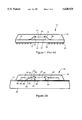
- an integrated circuit package generally designated by reference numeral 94 uses a different arrangement for electrically connecting package 94 to other elements.
- package 94 includes integrated circuit die 40, bonding wires 72, flex tape substrate 84, and encapsulating material 44 as were described above.
- flex tape substrate 84 has an outermost peripheral edge 96 and does not include contact terminals 66 on its bottom surface. Instead, electrically conductive traces, indicated by line 68, extend outwardly along the top surface of substrate 84 beyond peripheral edge 96 of substrate 84 rather than through substrate 84 as described in the previous embodiments.
- traces 68 are electrically connected to terminal pads 64 on the top surface of flex tape substrate 84, however, in this embodiment they extend outwardly along the top surface of substrate 84 beyond peripheral edge 96 rather than electrically connecting terminal pads 64 to contact terminals on the bottom surface of substrate 84. These traces which extend beyond outermost peripheral edge 96 allow integrated circuit package 94 to be electrically connected to other electrical elements such as a system board.
- package 94 may be mechanically attached to a system board 98 after it has been assembled in the manner described above.
- a thermally conductive adhesive 100 may be used to attach package 94 to the system board, thus providing good thermal dissipation of heat from the integrated circuit die.
- This overall arrangement provides an extremely thin integrated circuit package by eliminating the thickness of the solder ball contacts of the above described embodiments.
- an encapsulating material 102 may be formed over the exposed portions of traces 68 which extend beyond package 94. This encapsulating material would protect these outer portions of traces 68 from moisture and other corrosive elements.
- This same approach of extending the traces beyond the outermost peripheral edge of the package may be incorporated into integrated circuit package 36 described above to provide an even thinner integrated circuit package. This package would eliminate entirely the substrate thickness below the die as well as the thickness of the solder balls.
- the embodiments described above only include a single integrated circuit die 40, it should be understood that the present invention equally applies to integrated circuit packages having multiple die or other electronic devices in place of the integrated circuit die.
- the temporary support substrate carrier may take on a wide variety of forms. For example the carrier may be designed to support only one integrated circuit package at a time, or alternatively, may support a plurality of packages.
Abstract
A method of manufacturing an integrated circuit package assembly including (i) an integrated circuit die having a bottom surface and a plurality of input/output terminals, (ii) electrically conductive traces and/or contacts accessible from outside the assembly, and (iii) an encapsulating material encapsulating the integrated circuit die and portions of the electrically conductive traces and/or contacts will be disclosed. The method includes the following steps. First, a temporary support substrate or carrier having a top surface is provided for supporting the integrated circuit package as the package is being assembled. Then, the integrated circuit die is detachably supported on the top surface of the temporary support substrate. Each of the input/output terminals on the integrated circuit die are electrically connected to the electrically conductive traces and/or contacts. Next, the integrated circuit die and at least a portion of the electrically conductive traces and/or contacts are encapsulated with the encapsulating material such that the bottom surface of the integrated circuit die supported by the temporary support substrate is not covered by the encapsulating material. Finally, the encapsulated integrated circuit die is detached from the temporary support substrate.
Description
The present invention relates generally to integrated circuit packaging and more specifically to an Ultra Thin Ball Grid Array (UTBGA) integrated circuit package and a method of making the package which uses a temporary supporting substrate carrier to support the components of the package during the assembly of the package.
In the field of integrated circuit packaging, the cost and size of the overall package are major concerns. Any reduction in the cost of producing the package or reduction in the size or thickness of the package can provide a significant commercial advantage. To this end, the packaging of integrated circuits is continuously being improved to provide more cost effective designs and methods of producing integrated circuit packages.
There are currently several types of prior an Ball Grid Array (BGA) packages currently available. These prior an types include the Plastic Ball Grid Array (PBGA), the Ceramic Ball Grid Array (CBGA), and the Tape Ball Grid Array (TBGA). The PBGA and the TBGA are the thinnest ball grid array packages currently available. Referring to FIG. 1, a typical prior art PBGA integrated circuit package generally indicated by reference numeral 10 will be described. Prior art package 10 includes a dielectric substrate 12 an integrated circuit die 14, an array of bonding wires 16, an encapsulating material 18, and an array of contacts or solder balls 20.
As shown in FIG. 1, substrate 12 has a top surface 22, a bottom surface 24, a plurality of electrically conductive terminal pads 26 on the top surface 22 of substrate 12, a plurality of contact terminal pads 28 on the bottom surface 24 of substrate 12, and a plurality of electrically conductive traces (not shown). Each of the electrically conductive traces interconnects a respective one of terminal pads 26 on the top of substrate 12 to an associated contact terminal pad 28 on the bottom of substrate 12. Substrate 12 is made from a rigid material capable of supporting the other components of the package during the assembly of the package. Integrated circuit die 14 has a top surface 30, a bottom surface 32, and includes a plurality of input/output terminals 34 on its top surface 30. Each of the bonding wires 16 electrically connect a respective one of terminal pads 34 to an associated terminal pad 26 on the top surface of substrate 12. Encapsulating material 18 encapsulates integrated circuit die 14, at least the top surface of substrate 12, and bonding wires 16. Contacts or solder balls 20 are attached to associated contact terminal pads 28 thereby allowing external electrical elements to be electrically connected to integrated circuit die 14. This arrangement represents the typical prior art PBGA integrated circuit package.
The present invention provides a novel method of producing an Ultra Thin Ball Grid Array which can result in a PBGA package thinner than possible using prior art methods of producing BGA packages. This is accomplished by minimizing or eliminating the thickness of the substrate (i.e. substrate 12 of the prior art embodiment described above) and instead using a temporary supporting substrate or carrier to support the other components of an integrated circuit package during the assembly of the package. As will be described in more detail hereinafter, this novel method also provides a less expensive package by reducing the overall substrate cost by maximizing the substrate panel utilization as well as increase the substrate yield.
As will be described in more detail hereinafter, a method of manufacturing an integrated circuit package assembly including (i) an integrated circuit die having a bottom surface and a plurality of input/output terminals, (ii) electrically conductive traces and/or contacts accessible from outside the assembly, and (iii) an encapsulating material encapsulating the integrated circuit die and portions of the electrically conductive traces and/or contacts will be disclosed. The method includes the following steps. First, a temporary support substrate or carrier having a top surface is provided for supporting the integrated circuit package as the package is being assembled. Then, the integrated circuit die is detachably supported on the top surface of the temporary support substrate. Each of the input/output terminals on the integrated circuit die are electrically connected to the electrically conductive traces and/or contacts. Next, the integrated circuit die and at least a portion of the electrically conductive traces and/or contacts are encapsulated with the encapsulating material such that the bottom surface of the integrated circuit die supported by the temporary support substrate is not covered by the encapsulating material. Finally, the encapsulated integrated circuit die is detached from the temporary support substrate.
In one embodiment of the present invention, the integrated circuit package assembly includes a dielectric substrate, an integrated circuit die, an array of bonding wires, and an encapsulating material. The dielectric substrate has a horizontal top surface, a horizontal bottom surface, an outermost peripheral edge, a central opening defining an innermost edge, and a plurality of electrically conductive traces and/or contacts accessible from outside the assembly. The integrated circuit die has a horizontal top surface, a horizontal bottom surface, an outermost peripheral edge, and a plurality of input/output terminals. The integrated circuit die is positioned within the central opening of the substrate such that the bottom surface of the die and the bottom surface of the substrate substantially lie in a common plane. Each of the bonding wires making up the array of bonding wires electrically connects a respective one of the input/output terminals of the integrated circuit die to an associated one of the plurality of electrically conductive traces and/or contacts so that the die is electrically accessible from outside the assembly. And, the encapsulating material is integrally formed around and encapsulates the top surfaces and at least some of the edges of the substrate and the integrated circuit die and also surrounds and encapsulates the array of bonding wires such that the bottom surfaces of the substrate and die are not encapsulated by the integrally formed encapsulating material.
In another embodiment, the integrated circuit package assembly includes a dielectric flex tape substrate, and integrated circuit die, and an encapsulating material. The dielectric flex tape substrate has a horizontal top surface, a horizontal bottom surface, an outermost peripheral edge, and a plurality of electrically conductive traces and/or contacts accessible from outside the assembly. The integrated circuit die has a horizontal top surface, a horizontal bottom surface, an outermost peripheral edge, and a plurality of input/output terminals. The bottom surface of the integrated circuit die is attached to the top surface of the flex tape substrate. The integrated circuit package also includes a plurality of electrically conductive bonding wires or contacts for electrically connecting respective ones of the input/output terminals of the integrated circuit die to associated ones of the electrically conductive traces and/or contacts of the dielectric flex tape substrate. The encapsulating material is integrally formed around and encapsulating the top surface of the flex tape substrate, the top surface and peripheral edge of the integrated circuit die, and the electrically conductive bonding wires or contacts such that the bottom surface of the flex tape substrate is not encapsulated by the integrally formed encapsulating material. The flex tape substrate is sufficiently flexible such that it is not able to support by itself the integrated circuit die and the electrically conductive bonding wires or contacts without the support of the integrally formed encapsulating material.
The features of the present invention may best be understood by reference to the following description of the presently preferred embodiments together with the accompanying drawings in which:
FIG. 1 is a diagrammatic cross sectional view of a prior art plastic ball grid array integrated circuit package;
FIG. 2A is a diagrammatic cross sectional view of a first embodiment of an integrated circuit package in accordance with the present invention after being assembled on a temporary support substrate and before it is removed from the temporary support substrate;
FIG. 2B is a diagrammatic plan view of the integrated circuit package shown in FIG. 2A;
FIG. 3 is a diagrammatic cross sectional view of a second embodiment of an integrated circuit package in accordance with the present invention;
FIG. 4A through 4C are diagrammatic cross sectional views of three additional embodiments of an integrated circuit package in accordance with the present invention after being assembled on a temporary support substrate and before being removed from the temporary support substrate;
FIG. 5 is a diagrammatic orthographic view of a clamping arrangement for temporarily attaching a flex tape substrate to a temporary support substrate in accordance with the present invention as an integrated circuit package is assembled on the temporary support substrate; and
FIG. 6 is a diagrammatic cross sectional view of another embodiment of an integrated circuit package in accordance with the present invention.
Inasmuch as FIG. 1 was discussed previously, attention is directed to FIGS. 2-6 which illustrate integrated circuit packages in accordance with the present invention wherein like components are represented by like reference numerals. The integrated circuit packages shown in these figures are produced using the method of the present invention in which a temporary support substrate or carrier supports an integrated circuit die while the die is assembled into an integrated circuit package. The use of the temporary support substrate carrier eliminates the need to use a rigid substrate (i.e. substrate 12 of the prior art example described above) to support the die while the die is assembled into an integrated circuit package. By eliminating or significantly reducing the thickness of the substrate a thinner overall package may be produced.
Referring initially to FIGS. 2A and 2B, an integrated circuit package assembled using the method of the present invention and generally designated by reference numeral 36 will be described. Integrated circuit package 36 includes an integrated circuit die 40, a dielectric substrate 42, and an encapsulating material 44. Integrated circuit die 40 has a top surface 46, a bottom surface 48, an outermost peripheral edge 50, and includes a plurality of input/output terminals 52 located on top surface 46 of integrated circuit die 40. Dielectric substrate 42 has a top surface 54, a bottom surface 56, an outermost peripheral edge 58, and a central opening 60 defining an innermost edge 62. Dielectric substrate 42 also includes a plurality of terminal pads 64 on its top surface 54, an array of contact terminals 66 on its bottom surface 56, and a plurality of electrically conductive traces represented schematically by lines indicated by reference numeral 68. Each trace 68 electrically interconnects a respective one of the terminal pads 64 on the substrate's top surface to an associated contact terminal 66 on the substrate's bottom surface.
In accordance with the method being described, integrated circuit die 40 and substrate 42 are detachably supported on temporary support substrate carrier 38 such that integrated circuit die 40 is positioned within central opening 60 of substrate 42 and such that the bottom surfaces of die 40 and substrate 42 lie substantially in a common plane. In the embodiment shown in FIG. 2A, die 40 and substrate 42 are attached to substrate carrier 38 using a double sided adhesive tape material 70. One example of such an adhesive material is double sided polyimide tape. Although polyimide tape is given as one example of how die 40 and substrate 42 may be attached to substrate carrier 38, it should be understood that a wide variety of materials may be used. Reworkable adhesives such as thermoplastics, other types of double side adhesive tapes, and a wide variety of other attaching materials and mechanisms all fall within the spirit and scope of the described invention.
Integrated circuit package 36 further includes an array of bonding wires 72. Each bonding wire is electrically connected between a respective one of input/output terminals 52 on die 40 to an associated terminal pad 64 on substrate 42. This electrical connection of die 40 to substrate 42 allows integrated circuit die 40 to be electrically connected to other electrical elements through contact terminals 66 on bottom surface 56 of substrate 42 in the same manner as other conventional integrated circuit packages.
Once integrated circuit die 40 is electrically connected to substrate 42 using bonding wires 72, encapsulating material 44 is integrally formed around bonding wires 72 and the top surfaces and at least some of the edges of substrate 42 and die 40. This encapsulation of die 40 and substrate 42 mechanically interconnects die 40 and substrate 42 forming a rigid package which may now be removed from substrate carrier 38. As shown in FIG. 2A, this encapsulating material does not cover bottom surface 48 of die 40 and bottom surface 56 of substrate 42. Also, it should be noted that, in accordance with the present invention, until encapsulating material 44 is integrally formed around die 40 and substrate 42, substrate carrier 38 is required in order to provide a stable, rigid substrate for assembling package 36.
As shown in FIG. 3, after integrated circuit package 36 has been removed from temporary support substrate carrier 38, a plurality of electrically conductive contacts or solder balls are attached to respective ones of the contact terminals 66 on the bottom surface 56 of dielectric substrate 42. This is done in the conventional manner for ball grid array packages. Also, since bottom surface 48 of integrated circuit die 40 has not been encapsulated by encapsulating material 44, an additional covering material 76 may be applied to bottom surface 48 in order to protect die 40 from chipping or from moisture and other contaminants. In situations in which heat dissipation from die 40 is a specific concern, covering material 76 may be selected to be a particularly thermally conductive material. Alternatively, die 40 may be left uncovered so that it may be directly attached to a heat spreader or heat sink on a system board or device in which integrated circuit package 36 is ultimately going to be used. Therefore, the above described integrated circuit package provides a wide variety of options for dissipating heat from the integrated circuit die which are not typically available with prior art ball grid array packages.
As shown in FIG. 3 and in accordance with the present invention, integrated circuit package 36 is able to be manufactured thinner than other prior art packages. This is because the substrate which is required to support the integrated circuit die in prior art packages has been eliminated below the die. This elimination of the substrate below the die reduces the minimum thickness of the package by the thickness of the substrate (i.e. substrate 12 of the prior art package shown in FIG. 1) and the thickness of any die attach material typically used to attach the die to the substrate.
Although dielectric substrate 42 was shown as a single layered substrate in FIG. 2A, it should be understood that the present invention is not limited to single layered substrates. As shown in FIG. 3, dielectric substrate 42 may be a multi-layered dielectric substrate. Also, it should be understood that the dielectric substrate may take a wide variety of forms. Since the substrate is supported by the temporary support substrate carrier until encapsulated by the encapsulating material, the dielectric substrate itself is not required to be rigid. Therefore, substrate may be made up of a flexible material such as a dielectric flex tape substrate. Since flex tape substrates currently offer the highest trace densities compared to other substrates, the above described method allows for higher density plastic ball grid array packages than prior art PBGA packages. Alternatively, substrate 42 may be a printed wiring board or any other conventional substrate material and still remain within the scope of the present invention. Furthermore, although the substrate has been described and shown as having a central opening in which the die is located, it should be understood that the substrate may take on a wide variety of particular shapes. For example, the substrate may be made up of two separate strips positioned on opposite sides of the die and still remain within the spirit and scope of the present invention.
An additional advantage of the present invention is that it reduces the cost of the package by allowing for maximizing the panel utilization of the dielectric substrate and improving the yield of the substrate compared to the conventional methods. This is because each substrate is attached to the substrate carrier individually rather than in a strip form as in conventional methods. Therefore, defective substrates result in wasting only the one defective substrate rather than an entire strip of substrates. Also, using the individual substrates eliminates the need for an expensive singulation tool or die which is typically used to separate individual packages in conventional methods. Furthermore, since the die is not attached to the substrate in the conventional manner, no die attach material is used and no curing of the die attach material is required, further reducing the cost. Instead the die is directly attached to the adhesive tape or material on the temporary support substrate carrier using, for example, a standard die attaching machine.
Referring to FIGS. 4A-C, three additional embodiments of an integrated circuit package in accordance with the present invention and generally indicated by reference numerals 78, 80 and 82 respectively will be described. Integrated circuit package 78 is similar to the package described above in that it is assembled on temporary support substrate carrier 38 and it includes die 46, bonding wires 72, and encapsulating material 44. However, package 78 includes a dielectric flex tape substrate 84 having a top surface 86 and a bottom surface 88. Flex tape substrate 84 is attached to substrate carrier 38 in the same way as described above except that there is no opening formed in flex tape substrate 84 for die 40 to fit within. Instead bottom surface 48 of die 40 is attached to top surface 86 of substrate 84 using, for example, conventional die attach material 87. In accordance with the present invention, substrate 84 is sufficiently flexible that it is not able to, by itself, support integrated circuit die 40 without the support of either temporary support substrate carrier 38 during the assembly of the package or encapsulating material 44 after the assembly of the package. As described above for dielectric substrate 42, flex tape substrate 84 includes terminal pads 64 on its top surface, contact terminals 66 on its bottom surface and traces interconnecting respective terminal pads 64 to associated contact terminals 66 which are schematically represented by lines 68. Also as described above for package 36, an array of bonding wires 72 are electrically connected between respective input/output terminals on the top surface of die 40 and associated terminal pads 64 on the top surface of flex tape substrate 84. This allows other elements to be electrically connected to die 40 through the contact pads on the bottom of substrate 84.
Alternatively, as shown in FIG. 4B, die 40 may be electrically connected to substrate 84 using the flip chip method. With this method, an array of contacts or solder balls 90 are attached to the input/output terminals of die 40. Die 40 is then flipped over and solder balls 90 are used to electrically connect respective input/output terminals on die 40 to associated terminal pads on flex tape substrate 84. As shown in FIG. 4C, a combination of bonding wires and the flip chip method may be used to electrically connect die 40 to substrate 84 if the integrated circuit die has terminal pads formed on both its top and bottom surface.
Once the wire bonding process and/or the flip chip process is complete, encapsulating material 44 is integrally formed around bonding wires 72 (if present), integrated circuit die 40, and at least portions of the top surface 86 of substrate 84. This encapsulation of die 40 and substrate 84 forms a rigid package which may now be removed from substrate carrier 38. The encapsulating material does not cover bottom surface 88 of substrate 84 and, as described above, substrate carrier 38 is required in order to provide a stable, rigid substrate for assembling package 78, 80, and 82 until encapsulating material 44 is integrally formed around die 40 and on substrate 84.
In the same way as described above for package 36, after integrated circuit package 78, 80 and 82 have been removed from temporary support substrate carrier 38, a plurality of electrically conductive contacts or solder balls are attached to respective ones of the contact terminals on the bottom surface of flex tape substrate 84. With this described arrangement, the integrated circuit package is able to be manufactured thinner than other prior art packages. This is because the thickness of substrate 84 has been minimized and is substantially thinner than the substrate which is required to support the integrated circuit die in prior art packages. Also, as mentioned above, this method of producing an integrated circuit package allows a high trace density flex tape substrate to be used in a PBGA package therefore allowing a higher density PBGA package to be produced.
Referring to FIG. 5, alternative methods of attaching flex tape substrate 84 to temporary support substrate 38 may by used. For example, as illustrated in FIG. 5, a mechanical clamping arrangement may be employed. The particular embodiment of the clamping arrangement shown includes a clamping frame 92 which attaches to temporary support substrate carrier 38 using conventional clamping devices or fasteners. This arrangement mechanically holds substrate 84 in place as the assembly process proceeds. A wide variety of other mechanical clamping arrangements may be used and should be clear to those skilled in the art in view of the above disclosure.
In an additional embodiment illustrated in FIG. 6, an integrated circuit package generally designated by reference numeral 94 uses a different arrangement for electrically connecting package 94 to other elements. As shown in FIG. 6, package 94 includes integrated circuit die 40, bonding wires 72, flex tape substrate 84, and encapsulating material 44 as were described above. However, in this embodiment flex tape substrate 84 has an outermost peripheral edge 96 and does not include contact terminals 66 on its bottom surface. Instead, electrically conductive traces, indicated by line 68, extend outwardly along the top surface of substrate 84 beyond peripheral edge 96 of substrate 84 rather than through substrate 84 as described in the previous embodiments. As described above, traces 68 are electrically connected to terminal pads 64 on the top surface of flex tape substrate 84, however, in this embodiment they extend outwardly along the top surface of substrate 84 beyond peripheral edge 96 rather than electrically connecting terminal pads 64 to contact terminals on the bottom surface of substrate 84. These traces which extend beyond outermost peripheral edge 96 allow integrated circuit package 94 to be electrically connected to other electrical elements such as a system board.
As shown in FIG. 6, package 94 may be mechanically attached to a system board 98 after it has been assembled in the manner described above. For example, a thermally conductive adhesive 100 may be used to attach package 94 to the system board, thus providing good thermal dissipation of heat from the integrated circuit die. This overall arrangement provides an extremely thin integrated circuit package by eliminating the thickness of the solder ball contacts of the above described embodiments. Also, as indicated in FIG. 6, after traces 68 have been electrically connected to appropriate terminal pads or contacts on the system board, an encapsulating material 102 may be formed over the exposed portions of traces 68 which extend beyond package 94. This encapsulating material would protect these outer portions of traces 68 from moisture and other corrosive elements. This same approach of extending the traces beyond the outermost peripheral edge of the package may be incorporated into integrated circuit package 36 described above to provide an even thinner integrated circuit package. This package would eliminate entirely the substrate thickness below the die as well as the thickness of the solder balls.
Although the embodiments described above only include a single integrated circuit die 40, it should be understood that the present invention equally applies to integrated circuit packages having multiple die or other electronic devices in place of the integrated circuit die. Also, it should be understood that the temporary support substrate carrier may take on a wide variety of forms. For example the carrier may be designed to support only one integrated circuit package at a time, or alternatively, may support a plurality of packages.
Therefore, the present examples are to be considered as illustrative and not restrictive, and the invention is not to be limited to the details given herein, but may be modified within the scope of the appended claims.
Claims (21)
1. A method of manufacturing an integrated circuit package assembly including (i) an integrated circuit die having a bottom surface and a plurality of input/output terminals, (ii) electrically conductive means accessible from outside said assembly, and (iii) an encapsulating material encapsulating said integrated circuit die and portions of said electrically conductive means, said method comprising the steps of:
a) providing a temporary support substrate having a top surface for supporting said integrated circuit package as said package is being assembled;
b) detachably supporting said integrated circuit die on the top surface of said temporary support substrate;
c) electrically connecting each of said input/output terminals on said integrated circuit die to said electrically conductive means;
d) encapsulating said integrated circuit die and at least a portion of said electrically conductive means with said encapsulating material such that the bottom surface of said integrated circuit die supported by said temporary support substrate is not covered by said encapsulating material; and
f) detaching said encapsulated integrated circuit die from said temporary support substrate.
2. A method according to claim 1 including a dielectric substrate at least in part providing said electrically conductive means, said dielectric substrate having a horizontal top surface, a horizontal bottom surface, an outermost peripheral edge, and a central opening defining an innermost edge, and wherein said step of detachably supporting said integrated circuit die on the top surface of said temporary support substrate includes the step of detachably attaching said integrated circuit die directly on said temporary support substrate within said central opening of said dielectric substrate and detachably attaching said dielectric substrate directly on said temporary support substrate such that the bottom surface of said die and the bottom surface of said dielectric substrate substantially lie in common plane.
3. A method according to claim 2 wherein said dielectric substrate is a multi-layered substrate having a plurality of vertically stepped horizontal top surfaces along said innermost edge corresponding to the layers making up the multi-layered substrate.
4. A method according to claim 2 wherein said dielectric substrate and said integrated circuit die are detachably attached directly to said temporary support substrate using a double sided polyimide adhesive tape.
5. A method according to claim 2 wherein said dielectric substrate is a dielectric polyimide flex tape.
6. A method according to claim 2 wherein said dielectric substrate is a printed wiring board.
7. A method according to claim 2 wherein;
a) said dielectric substrate includes a plurality of contact terminals on the bottom surface of said dielectric substrate, a plurality of terminal pads on the top surface of said dielectric substrate, and a plurality of traces, each of said traces of said dielectric substrate electrically connecting a respective one of said contact terminals on the bottom of said dielectric substrate to an associated one of said terminal pads on the top surface of said dielectric substrate, and
b) said method further includes the step of, after the step of detaching said encapsulated integrated circuit die from said temporary support substrate, attaching an array of electrically conductive contacts to respective ones of said contact terminals on the bottom of said dielectric substrate, said contacts providing means for electrically connecting said integrated circuit package to other electrical elements.
8. A method according to claim 7 wherein said contacts are solder balls.
9. A method according to claim 7 further including the step of covering the bottom surface of said integrated circuit die with material apart from said encapsulating material.
10. A method according to claim 2 wherein said dielectric substrate includes a plurality of traces extending outwardly beyond the outermost peripheral edge of said dielectric substrate which are adapted to electrically connect said integrated circuit package to other electrical elements.
11. A method according to claim 1 including a dielectric flex tape substrate providing at least a portion of said electrically conductive means, said dielectric flex tape substrate having a horizontal top surface and a horizontal bottom surface and said dielectric flex tape substrate being sufficiently flexible such that it is not able to support by itself said integrated circuit die and said electrically conductive means without the support of said temporary support substrate and wherein said step of detachably supporting said integrated circuit die on the top surface of said temporary support substrate includes the step of detachably attaching said dielectric flex tape substrate directly on said temporary support substrate and the step of attaching said integrated circuit die to the top surface of said dielectric flex tape substrate.
12. A method according to claim 11 wherein said dielectric flex tape substrate is detachably attached to said carrier plate using a double sided polyimide adhesive tape.
13. A method according to claim 11 wherein said dielectric flex tape substrate is detachably attached to said carrier plate using a mechanical clamping arrangement.
14. A method according to claim 11 wherein:
a) said input/output terminal pads on said integrated circuit die are located on said bottom surface of said integrated circuit die;
b) said dielectric flex tape substrate includes a plurality of terminal pads on the top surface of said dielectric flex tape substrate; and
c) said the step of attaching said integrated circuit die to the top surface of said dielectric flex tape substrate includes the step of using an array of contacts to electrically interconnect respective ones of said input/output terminal pads on said integrated circuit die to associated terminal pads on the top surface of said flex tape substrate.
15. A method according to claim 14 wherein said contacts are solder balls.
16. A method according to claim 14 wherein:
a) said integrated circuit die includes additional input/output terminal pads located on the top surface of said integrated circuit die; and
b) said step of attaching said integrated circuit die to the top surface of said dielectric flex tape substrate further includes the step of using an array of bonding wires to electrically interconnect respective ones of said additional input/output terminal pads on the top surface of said integrated circuit die to associated terminal pads on the top surface of said dielectric flex tape substrate.
17. A method according to claim 11 wherein:
a) said input/output terminal pads on said integrated circuit die are located on the top surface of said integrated circuit die;
b) said dielectric flex tape substrate includes a plurality of terminal pads on the top surface of said dielectric flex tape substrate; and
c) said step of attaching said integrated circuit die to said top surface of said dielectric flex tape substrate includes the step of using an array of bonding wires to electrically interconnect respective ones of said input/output terminal pads on said integrated circuit die to associated terminal pads on the top surface of said dielectric flex tape substrate.
18. A method according to claim 11 wherein said dielectric flex tape substrate is a polyimide tape.
19. A method according to claim 11 wherein:
a) said dielectric flex tape substrate includes a plurality of contact terminals on the bottom surface of said dielectric flex tape substrate, a plurality of terminal pads on the top surface of said dielectric flex tape substrate, and a plurality of traces, each of said traces electrically connecting a respective one of said contact terminals on the bottom of said substrate to an associated one of said terminal pads on the top surface of said substrate, and
b) said method further includes the step of attaching an array of electrically conductive contacts to respective ones of said contact terminals on the bottom of said dielectric flex tape substrate for electrically connecting said integrated circuit package to external electrical elements.
20. A method according to claim 19 wherein said contacts are solder balls.
21. A method according to claim 11 wherein said dielectric flex tape substrate includes a plurality of traces extending outwardly beyond the outermost peripheral edge of said dielectric flex tape substrate, said traces being adapted to electrically connect said integrated circuit package to other electrical elements.
Priority Applications (4)
| Application Number | Priority Date | Filing Date | Title |
|---|---|---|---|
| US08/439,362 US5620928A (en) | 1995-05-11 | 1995-05-11 | Ultra thin ball grid array using a flex tape or printed wiring board substrate and method |
| EP96920486A EP0842533A1 (en) | 1995-05-11 | 1996-05-24 | Ultra thin ball grid array package using a flex tape or printed wiring board substrate and method |
| PCT/US1996/007698 WO1997044822A1 (en) | 1995-05-11 | 1996-05-24 | Ultra thin ball grid array package using a flex tape or printed wiring board substrate and method |
| KR1019970700165A KR970705178A (en) | 1995-05-11 | 1997-01-11 | ULTRA THIN BALL GRID ARRAY USING A FLEX TAPE OR PRINTED WIRING BOARD SUBSTRATE AND METHOD |
Applications Claiming Priority (2)
| Application Number | Priority Date | Filing Date | Title |
|---|---|---|---|
| US08/439,362 US5620928A (en) | 1995-05-11 | 1995-05-11 | Ultra thin ball grid array using a flex tape or printed wiring board substrate and method |
| PCT/US1996/007698 WO1997044822A1 (en) | 1995-05-11 | 1996-05-24 | Ultra thin ball grid array package using a flex tape or printed wiring board substrate and method |
Publications (1)
| Publication Number | Publication Date |
|---|---|
| US5620928A true US5620928A (en) | 1997-04-15 |
Family
ID=1341175
Family Applications (1)
| Application Number | Title | Priority Date | Filing Date |
|---|---|---|---|
| US08/439,362 Expired - Lifetime US5620928A (en) | 1995-05-11 | 1995-05-11 | Ultra thin ball grid array using a flex tape or printed wiring board substrate and method |
Country Status (4)
| Country | Link |
|---|---|
| US (1) | US5620928A (en) |
| EP (1) | EP0842533A1 (en) |
| KR (1) | KR970705178A (en) |
| WO (1) | WO1997044822A1 (en) |
Cited By (65)
| Publication number | Priority date | Publication date | Assignee | Title |
|---|---|---|---|---|
| US5830800A (en) * | 1997-04-11 | 1998-11-03 | Compeq Manufacturing Company Ltd. | Packaging method for a ball grid array integrated circuit without utilizing a base plate |
| US5835355A (en) * | 1997-09-22 | 1998-11-10 | Lsi Logic Corporation | Tape ball grid array package with perforated metal stiffener |
| US5852870A (en) * | 1996-04-24 | 1998-12-29 | Amkor Technology, Inc. | Method of making grid array assembly |
| US5885848A (en) * | 1996-09-30 | 1999-03-23 | Lsi Logic Corporation | Ball grid array with inexpensive threaded secure locking mechanism to allow removal of a threaded heat sink therefrom |
| US5888847A (en) * | 1995-12-08 | 1999-03-30 | Lsi Logic Corporation | Technique for mounting a semiconductor die |
| US5943769A (en) * | 1994-06-21 | 1999-08-31 | Giesecke & Devrient Gmbh | Method for producing integrated circuits and coils on carrier webs |
| US5953589A (en) * | 1996-12-30 | 1999-09-14 | Anam Semiconductor Inc. | Ball grid array semiconductor package with solder balls fused on printed circuit board and method for fabricating the same |
| US5963792A (en) * | 1998-02-05 | 1999-10-05 | Micron Technology, Inc. | Use of an oxide surface to facilitate gate break on a carrier substrate for a semiconductor device |
| US6100113A (en) * | 1998-07-13 | 2000-08-08 | Institute Of Microelectronics | Very thin multi-chip-package and method of mass producing the same |
| US6111324A (en) * | 1998-02-05 | 2000-08-29 | Asat, Limited | Integrated carrier ring/stiffener and method for manufacturing a flexible integrated circuit package |
| US6172419B1 (en) | 1998-02-24 | 2001-01-09 | Micron Technology, Inc. | Low profile ball grid array package |
| US6247229B1 (en) | 1999-08-25 | 2001-06-19 | Ankor Technology, Inc. | Method of forming an integrated circuit device package using a plastic tape as a base |
| US6340846B1 (en) | 2000-12-06 | 2002-01-22 | Amkor Technology, Inc. | Making semiconductor packages with stacked dies and reinforced wire bonds |
| US6348399B1 (en) * | 2000-07-06 | 2002-02-19 | Advanced Semiconductor Engineering, Inc. | Method of making chip scale package |
| US6395578B1 (en) | 1999-05-20 | 2002-05-28 | Amkor Technology, Inc. | Semiconductor package and method for fabricating the same |
| US6408510B1 (en) | 1998-02-13 | 2002-06-25 | Micron Technology, Inc. | Method for making chip scale packages |
| WO2002063683A2 (en) | 2001-02-09 | 2002-08-15 | Koninklijke Philips Electronics N.V. | Method of manufacturing a semiconductor device and a semiconductor device obtained by means of said method |
| US20020114144A1 (en) * | 2000-12-19 | 2002-08-22 | Takashi Kumamoto | Molded flip chip package |
| US6452278B1 (en) | 2000-06-30 | 2002-09-17 | Amkor Technology, Inc. | Low profile package for plural semiconductor dies |
| US6469258B1 (en) | 1999-08-24 | 2002-10-22 | Amkor Technology, Inc. | Circuit board for semiconductor package |
| US6472758B1 (en) | 2000-07-20 | 2002-10-29 | Amkor Technology, Inc. | Semiconductor package including stacked semiconductor dies and bond wires |
| US6486537B1 (en) | 2001-03-19 | 2002-11-26 | Amkor Technology, Inc. | Semiconductor package with warpage resistant substrate |
| US6501184B1 (en) | 1999-05-20 | 2002-12-31 | Amkor Technology, Inc. | Semiconductor package and method for manufacturing the same |
| US20030011064A1 (en) * | 2001-07-11 | 2003-01-16 | Combs Edward G. | Enhanced thermal dissipation integrated circuit package and method of manufacturing enhanced thermal dissipation integrated circuit package |
| SG93900A1 (en) * | 2000-08-09 | 2003-01-21 | Kostat Semiconductor Co Ltd | Semiconductor package having implantable conductive lands and method for manufacturing the same |
| US6512288B1 (en) | 1999-06-07 | 2003-01-28 | Amkor Technology, Inc. | Circuit board semiconductor package |
| US6515356B1 (en) | 1999-05-07 | 2003-02-04 | Amkor Technology, Inc. | Semiconductor package and method for fabricating the same |
| WO2003017328A2 (en) * | 2001-08-15 | 2003-02-27 | Asat Limited | Encapsulated integrated circuit package and method of manufacturing an integrated circuit package |
| US6531784B1 (en) | 2000-06-02 | 2003-03-11 | Amkor Technology, Inc. | Semiconductor package with spacer strips |
| US6534338B1 (en) | 2001-06-29 | 2003-03-18 | Amkor Technology, Inc. | Method for molding semiconductor package having a ceramic substrate |
| US6537848B2 (en) | 2001-05-30 | 2003-03-25 | St. Assembly Test Services Ltd. | Super thin/super thermal ball grid array package |
| US6543512B1 (en) * | 1998-10-28 | 2003-04-08 | Micron Technology, Inc. | Carrier, method and system for handling semiconductor components |
| US6544812B1 (en) | 2000-11-06 | 2003-04-08 | St Assembly Test Service Ltd. | Single unit automated assembly of flex enhanced ball grid array packages |
| US6576998B1 (en) | 2002-02-28 | 2003-06-10 | Amkor Technology, Inc. | Thin semiconductor package with semiconductor chip and electronic discrete device |
| US6577013B1 (en) | 2000-09-05 | 2003-06-10 | Amkor Technology, Inc. | Chip size semiconductor packages with stacked dies |
| US6586677B2 (en) | 1999-08-25 | 2003-07-01 | Amkor Technology, Inc. | Plastic integrated circuit device package having exposed lead surface |
| US20030138980A1 (en) * | 1996-01-02 | 2003-07-24 | Moden Walter L. | Method of temporarily securing a die to a burn-in carrier |
| US20030143781A1 (en) * | 2002-01-31 | 2003-07-31 | Mclellan Neil Robert | Encapsulated integrated circuit package and method of manufacturing an integrated circuit package |
| US6624005B1 (en) | 2000-09-06 | 2003-09-23 | Amkor Technology, Inc. | Semiconductor memory cards and method of making same |
| US20030234454A1 (en) * | 2002-06-24 | 2003-12-25 | Serafin Pedron | Integrated circuit package and method of manufacturing the integrated circuit package |
| US20040007771A1 (en) * | 1999-08-24 | 2004-01-15 | Amkor Technology, Inc. | Semiconductor package and method for fabricating the smae |
| US20040017668A1 (en) * | 2002-07-26 | 2004-01-29 | Stmicroelectronics, Inc. | Leadframeless package structure and method |
| US20040046241A1 (en) * | 2002-03-22 | 2004-03-11 | Combs Edward G. | Method of manufacturing enhanced thermal dissipation integrated circuit package |
| US6737299B1 (en) | 1999-06-08 | 2004-05-18 | Micron Technology, Inc. | Thermally conductive adhesive tape for semiconductor devices and method for using the same |
| US20040224149A1 (en) * | 1996-05-30 | 2004-11-11 | Akira Nagai | Circuit tape having adhesive film semiconductor device and a method for manufacturing the same |
| US6848173B2 (en) * | 1994-07-07 | 2005-02-01 | Tessera, Inc. | Microelectric packages having deformed bonded leads and methods therefor |
| US6858922B2 (en) * | 2001-01-19 | 2005-02-22 | International Rectifier Corporation | Back-to-back connected power semiconductor device package |
| US20050176180A1 (en) * | 2004-02-09 | 2005-08-11 | Fay Owen R. | Die encapsulation using a porous carrier |
| US6936922B1 (en) | 2003-09-26 | 2005-08-30 | Amkor Technology, Inc. | Semiconductor package structure reducing warpage and manufacturing method thereof |
| US7015072B2 (en) | 2001-07-11 | 2006-03-21 | Asat Limited | Method of manufacturing an enhanced thermal dissipation integrated circuit package |
| US20060117332A1 (en) * | 2004-11-30 | 2006-06-01 | Manabu Ochi | Optical pick-up |
| US7061123B1 (en) | 2004-05-03 | 2006-06-13 | National Semiconductor Corporation | Wafer level ball grid array |
| US20070117268A1 (en) * | 2005-11-23 | 2007-05-24 | Baker Hughes, Inc. | Ball grid attachment |
| US20070145548A1 (en) * | 2003-12-22 | 2007-06-28 | Amkor Technology, Inc. | Stack-type semiconductor package and manufacturing method thereof |
| US20070246544A1 (en) * | 2006-04-20 | 2007-10-25 | Sheila Yang | Method for manufacturing memory card structure |
| USRE40112E1 (en) | 1999-05-20 | 2008-02-26 | Amkor Technology, Inc. | Semiconductor package and method for fabricating the same |
| US20080088978A1 (en) * | 2006-10-11 | 2008-04-17 | Nitto Denko Corporation | Heat transfer for a hard-drive wire-bond pre-amp |
| US20080088977A1 (en) * | 2006-10-11 | 2008-04-17 | Nitto Denko Corporation | Heat transfer for a hard-drive pre-amp |
| US20080182363A1 (en) * | 2007-01-31 | 2008-07-31 | Freescale Semiconductor, Inc. | Method for forming a microelectronic assembly including encapsulating a die using a sacrificial layer |
| US20090121352A1 (en) * | 2005-06-20 | 2009-05-14 | Via Technologies, Inc. | Mutli-package module and electronic device using the same |
| US20100035405A1 (en) * | 2008-08-07 | 2010-02-11 | Win Semiconductors Corp. | Method for mounting a thinned semiconductor wafer on a carrier substrate |
| US9048306B2 (en) | 2009-09-23 | 2015-06-02 | Stats Chippac, Ltd. | Semiconductor device and method of forming open cavity in TSV interposer to contain semiconductor die in WLCSMP |
| US20150364373A1 (en) * | 2014-06-11 | 2015-12-17 | Texas Instruments Incorporated | Quad Flat No Lead Package And Method Of Making |
| US9466545B1 (en) | 2007-02-21 | 2016-10-11 | Amkor Technology, Inc. | Semiconductor package in package |
| US9875911B2 (en) | 2009-09-23 | 2018-01-23 | STATS ChipPAC Pte. Ltd. | Semiconductor device and method of forming interposer with opening to contain semiconductor die |
Citations (5)
| Publication number | Priority date | Publication date | Assignee | Title |
|---|---|---|---|---|
| US5102829A (en) * | 1991-07-22 | 1992-04-07 | At&T Bell Laboratories | Plastic pin grid array package |
| US5292688A (en) * | 1990-03-14 | 1994-03-08 | International Business Machines Corporation | Solder interconnection structure on organic substrates and process for making |
| US5340771A (en) * | 1993-03-18 | 1994-08-23 | Lsi Logic Corporation | Techniques for providing high I/O count connections to semiconductor dies |
| US5474958A (en) * | 1993-05-04 | 1995-12-12 | Motorola, Inc. | Method for making semiconductor device having no die supporting surface |
| US5490324A (en) * | 1993-09-15 | 1996-02-13 | Lsi Logic Corporation | Method of making integrated circuit package having multiple bonding tiers |
Family Cites Families (8)
| Publication number | Priority date | Publication date | Assignee | Title |
|---|---|---|---|---|
| FR2524707B1 (en) * | 1982-04-01 | 1985-05-31 | Cit Alcatel | METHOD OF ENCAPSULATION OF SEMICONDUCTOR COMPONENTS, AND ENCAPSULATED COMPONENTS OBTAINED |
| JP2840316B2 (en) * | 1989-09-06 | 1998-12-24 | 新光電気工業株式会社 | Semiconductor device and manufacturing method thereof |
| JPH04119653A (en) * | 1990-09-11 | 1992-04-21 | Toppan Printing Co Ltd | Integrated circuit element |
| JPH04267545A (en) * | 1991-02-22 | 1992-09-24 | Nec Corp | Plastic molded type semiconductor device |
| US5218759A (en) * | 1991-03-18 | 1993-06-15 | Motorola, Inc. | Method of making a transfer molded semiconductor device |
| JPH05102212A (en) * | 1991-10-04 | 1993-04-23 | Seiko Epson Corp | Wiring substrate |
| JPH05102337A (en) * | 1991-10-04 | 1993-04-23 | Seiko Epson Corp | Wiring board |
| GB2293918A (en) * | 1994-10-06 | 1996-04-10 | Ibm | Electronic circuit packaging |
-
1995
- 1995-05-11 US US08/439,362 patent/US5620928A/en not_active Expired - Lifetime
-
1996
- 1996-05-24 EP EP96920486A patent/EP0842533A1/en not_active Withdrawn
- 1996-05-24 WO PCT/US1996/007698 patent/WO1997044822A1/en not_active Application Discontinuation
-
1997
- 1997-01-11 KR KR1019970700165A patent/KR970705178A/en not_active IP Right Cessation
Patent Citations (5)
| Publication number | Priority date | Publication date | Assignee | Title |
|---|---|---|---|---|
| US5292688A (en) * | 1990-03-14 | 1994-03-08 | International Business Machines Corporation | Solder interconnection structure on organic substrates and process for making |
| US5102829A (en) * | 1991-07-22 | 1992-04-07 | At&T Bell Laboratories | Plastic pin grid array package |
| US5340771A (en) * | 1993-03-18 | 1994-08-23 | Lsi Logic Corporation | Techniques for providing high I/O count connections to semiconductor dies |
| US5474958A (en) * | 1993-05-04 | 1995-12-12 | Motorola, Inc. | Method for making semiconductor device having no die supporting surface |
| US5490324A (en) * | 1993-09-15 | 1996-02-13 | Lsi Logic Corporation | Method of making integrated circuit package having multiple bonding tiers |
Cited By (121)
| Publication number | Priority date | Publication date | Assignee | Title |
|---|---|---|---|---|
| US5943769A (en) * | 1994-06-21 | 1999-08-31 | Giesecke & Devrient Gmbh | Method for producing integrated circuits and coils on carrier webs |
| US6848173B2 (en) * | 1994-07-07 | 2005-02-01 | Tessera, Inc. | Microelectric packages having deformed bonded leads and methods therefor |
| US20050155223A1 (en) * | 1994-07-07 | 2005-07-21 | Tessera, Inc. | Methods of making microelectronic assemblies |
| US5888847A (en) * | 1995-12-08 | 1999-03-30 | Lsi Logic Corporation | Technique for mounting a semiconductor die |
| US20030206034A1 (en) * | 1996-01-02 | 2003-11-06 | Moden Walter L. | Method of temporarily securing a die to a burn-in carrier |
| US6894521B2 (en) | 1996-01-02 | 2005-05-17 | Micron Technology, Inc. | Burn-in carrier for a semiconductor die |
| US7105380B2 (en) * | 1996-01-02 | 2006-09-12 | Micron Technology, Inc. | Method of temporarily securing a die to a burn-in carrier |
| US20030138980A1 (en) * | 1996-01-02 | 2003-07-24 | Moden Walter L. | Method of temporarily securing a die to a burn-in carrier |
| US20050272172A1 (en) * | 1996-01-02 | 2005-12-08 | Moden Walter L | Method of temporarily securing a die to a burn-in carrier |
| US6329606B1 (en) | 1996-04-24 | 2001-12-11 | Amkor Technology, Inc. | Grid array assembly of circuit boards with singulation grooves |
| US5852870A (en) * | 1996-04-24 | 1998-12-29 | Amkor Technology, Inc. | Method of making grid array assembly |
| US20040224149A1 (en) * | 1996-05-30 | 2004-11-11 | Akira Nagai | Circuit tape having adhesive film semiconductor device and a method for manufacturing the same |
| US7202570B2 (en) * | 1996-05-30 | 2007-04-10 | Renesas Technology Corp. | Circuit tape having adhesive film semiconductor device and a method for manufacturing the same |
| US5885848A (en) * | 1996-09-30 | 1999-03-23 | Lsi Logic Corporation | Ball grid array with inexpensive threaded secure locking mechanism to allow removal of a threaded heat sink therefrom |
| US5953589A (en) * | 1996-12-30 | 1999-09-14 | Anam Semiconductor Inc. | Ball grid array semiconductor package with solder balls fused on printed circuit board and method for fabricating the same |
| US5830800A (en) * | 1997-04-11 | 1998-11-03 | Compeq Manufacturing Company Ltd. | Packaging method for a ball grid array integrated circuit without utilizing a base plate |
| US5835355A (en) * | 1997-09-22 | 1998-11-10 | Lsi Logic Corporation | Tape ball grid array package with perforated metal stiffener |
| US6404069B2 (en) | 1998-02-05 | 2002-06-11 | Micron Technology, Inc. | Use of oxide surface to facilitate gate break on a carrier substrate for a semiconductor device |
| US6545368B2 (en) | 1998-02-05 | 2003-04-08 | Micron Technology, Inc. | Use of an oxide surface to facilitate gate break on a carrier substrate for a semiconductor device |
| US6251702B1 (en) | 1998-02-05 | 2001-06-26 | Micron Technology, Inc. | Use of an oxide surface to facilitate gate break on a carrier substrate for a semiconductor device |
| US6111324A (en) * | 1998-02-05 | 2000-08-29 | Asat, Limited | Integrated carrier ring/stiffener and method for manufacturing a flexible integrated circuit package |
| US5963792A (en) * | 1998-02-05 | 1999-10-05 | Micron Technology, Inc. | Use of an oxide surface to facilitate gate break on a carrier substrate for a semiconductor device |
| US6408510B1 (en) | 1998-02-13 | 2002-06-25 | Micron Technology, Inc. | Method for making chip scale packages |
| US6798063B2 (en) | 1998-02-24 | 2004-09-28 | Micron Technology, Inc. | Low profile ball grid array package |
| US6172419B1 (en) | 1998-02-24 | 2001-01-09 | Micron Technology, Inc. | Low profile ball grid array package |
| US6344688B1 (en) | 1998-07-13 | 2002-02-05 | Institute Of Microelectronics | Very thin multi-chip package and method of mass producing the same |
| US6100113A (en) * | 1998-07-13 | 2000-08-08 | Institute Of Microelectronics | Very thin multi-chip-package and method of mass producing the same |
| US6543512B1 (en) * | 1998-10-28 | 2003-04-08 | Micron Technology, Inc. | Carrier, method and system for handling semiconductor components |
| US6579399B1 (en) | 1998-10-28 | 2003-06-17 | Micron Technology Inc | Method and system for handling semiconductor components |
| US6717248B2 (en) | 1999-05-07 | 2004-04-06 | Amkor Technology, Inc. | Semiconductor package and method for fabricating the same |
| US7190071B2 (en) | 1999-05-07 | 2007-03-13 | Amkor Technology, Inc. | Semiconductor package and method for fabricating the same |
| US6515356B1 (en) | 1999-05-07 | 2003-02-04 | Amkor Technology, Inc. | Semiconductor package and method for fabricating the same |
| US20040164411A1 (en) * | 1999-05-07 | 2004-08-26 | Amkor Technology, Inc. | Semiconductor package and method for fabricating the same |
| US7061120B2 (en) | 1999-05-20 | 2006-06-13 | Amkor Technology, Inc. | Stackable semiconductor package having semiconductor chip within central through hole of substrate |
| US6830955B2 (en) | 1999-05-20 | 2004-12-14 | Amkor Technology, Inc. | Semiconductor package and method for manufacturing the same |
| US20040175916A1 (en) * | 1999-05-20 | 2004-09-09 | Amkor Technology, Inc. | Stackable semiconductor package having semiconductor chip within central through hole of substrate |
| US6395578B1 (en) | 1999-05-20 | 2002-05-28 | Amkor Technology, Inc. | Semiconductor package and method for fabricating the same |
| US6762078B2 (en) | 1999-05-20 | 2004-07-13 | Amkor Technology, Inc. | Semiconductor package having semiconductor chip within central aperture of substrate |
| US20030001285A1 (en) * | 1999-05-20 | 2003-01-02 | Amkor Technology, Inc. | Semiconductor package and method for manufacturing the same |
| US6501184B1 (en) | 1999-05-20 | 2002-12-31 | Amkor Technology, Inc. | Semiconductor package and method for manufacturing the same |
| USRE40112E1 (en) | 1999-05-20 | 2008-02-26 | Amkor Technology, Inc. | Semiconductor package and method for fabricating the same |
| US6512288B1 (en) | 1999-06-07 | 2003-01-28 | Amkor Technology, Inc. | Circuit board semiconductor package |
| US6737299B1 (en) | 1999-06-08 | 2004-05-18 | Micron Technology, Inc. | Thermally conductive adhesive tape for semiconductor devices and method for using the same |
| US20040007771A1 (en) * | 1999-08-24 | 2004-01-15 | Amkor Technology, Inc. | Semiconductor package and method for fabricating the smae |
| US6982488B2 (en) | 1999-08-24 | 2006-01-03 | Amkor Technology, Inc. | Semiconductor package and method for fabricating the same |
| US6469258B1 (en) | 1999-08-24 | 2002-10-22 | Amkor Technology, Inc. | Circuit board for semiconductor package |
| US20050205979A1 (en) * | 1999-08-24 | 2005-09-22 | Shin Won S | Semiconductor package and method for fabricating the same |
| US6798049B1 (en) | 1999-08-24 | 2004-09-28 | Amkor Technology Inc. | Semiconductor package and method for fabricating the same |
| US7211900B2 (en) | 1999-08-24 | 2007-05-01 | Amkor Technology, Inc. | Thin semiconductor package including stacked dies |
| US6586677B2 (en) | 1999-08-25 | 2003-07-01 | Amkor Technology, Inc. | Plastic integrated circuit device package having exposed lead surface |
| US6247229B1 (en) | 1999-08-25 | 2001-06-19 | Ankor Technology, Inc. | Method of forming an integrated circuit device package using a plastic tape as a base |
| US6531784B1 (en) | 2000-06-02 | 2003-03-11 | Amkor Technology, Inc. | Semiconductor package with spacer strips |
| US6452278B1 (en) | 2000-06-30 | 2002-09-17 | Amkor Technology, Inc. | Low profile package for plural semiconductor dies |
| US6348399B1 (en) * | 2000-07-06 | 2002-02-19 | Advanced Semiconductor Engineering, Inc. | Method of making chip scale package |
| US6472758B1 (en) | 2000-07-20 | 2002-10-29 | Amkor Technology, Inc. | Semiconductor package including stacked semiconductor dies and bond wires |
| US6650019B2 (en) | 2000-07-20 | 2003-11-18 | Amkor Technology, Inc. | Method of making a semiconductor package including stacked semiconductor dies |
| SG93900A1 (en) * | 2000-08-09 | 2003-01-21 | Kostat Semiconductor Co Ltd | Semiconductor package having implantable conductive lands and method for manufacturing the same |
| US6577013B1 (en) | 2000-09-05 | 2003-06-10 | Amkor Technology, Inc. | Chip size semiconductor packages with stacked dies |
| US6624005B1 (en) | 2000-09-06 | 2003-09-23 | Amkor Technology, Inc. | Semiconductor memory cards and method of making same |
| US8258613B1 (en) | 2000-09-06 | 2012-09-04 | Amkor Technology, Inc. | Semiconductor memory card |
| US6759752B2 (en) | 2000-11-06 | 2004-07-06 | St Assembly Test Services Ltd. | Single unit automated assembly of flex enhanced ball grid array packages |
| US6544812B1 (en) | 2000-11-06 | 2003-04-08 | St Assembly Test Service Ltd. | Single unit automated assembly of flex enhanced ball grid array packages |
| US6340846B1 (en) | 2000-12-06 | 2002-01-22 | Amkor Technology, Inc. | Making semiconductor packages with stacked dies and reinforced wire bonds |
| US20020114144A1 (en) * | 2000-12-19 | 2002-08-22 | Takashi Kumamoto | Molded flip chip package |
| US6858922B2 (en) * | 2001-01-19 | 2005-02-22 | International Rectifier Corporation | Back-to-back connected power semiconductor device package |
| WO2002063683A2 (en) | 2001-02-09 | 2002-08-15 | Koninklijke Philips Electronics N.V. | Method of manufacturing a semiconductor device and a semiconductor device obtained by means of said method |
| US20020119594A1 (en) * | 2001-02-09 | 2002-08-29 | Van Veen Nicolaas Johannes Anthonius | Method of manufacturing a semiconductor device and a semiconductor device obtained by means of said method |
| WO2002063683A3 (en) * | 2001-02-09 | 2002-10-10 | Koninkl Philips Electronics Nv | Method of manufacturing a semiconductor device and a semiconductor device obtained by means of said method |
| US6890797B2 (en) | 2001-02-09 | 2005-05-10 | Koninklijke Philips Electronics N.V. | Method of making a surface mountable semiconductor device using a flexible foil and a semiconductor device obtained by means of said method |
| US6486537B1 (en) | 2001-03-19 | 2002-11-26 | Amkor Technology, Inc. | Semiconductor package with warpage resistant substrate |
| US6537848B2 (en) | 2001-05-30 | 2003-03-25 | St. Assembly Test Services Ltd. | Super thin/super thermal ball grid array package |
| US6744125B2 (en) | 2001-05-30 | 2004-06-01 | St. Assembly Test Services Ltd. | Super thin/super thermal ball grid array package |
| US6534338B1 (en) | 2001-06-29 | 2003-03-18 | Amkor Technology, Inc. | Method for molding semiconductor package having a ceramic substrate |
| US20030011064A1 (en) * | 2001-07-11 | 2003-01-16 | Combs Edward G. | Enhanced thermal dissipation integrated circuit package and method of manufacturing enhanced thermal dissipation integrated circuit package |
| US7015072B2 (en) | 2001-07-11 | 2006-03-21 | Asat Limited | Method of manufacturing an enhanced thermal dissipation integrated circuit package |
| US6734552B2 (en) | 2001-07-11 | 2004-05-11 | Asat Limited | Enhanced thermal dissipation integrated circuit package |
| WO2003017328A2 (en) * | 2001-08-15 | 2003-02-27 | Asat Limited | Encapsulated integrated circuit package and method of manufacturing an integrated circuit package |
| WO2003017328A3 (en) * | 2001-08-15 | 2003-11-13 | Asat Ltd | Encapsulated integrated circuit package and method of manufacturing an integrated circuit package |
| US20050077613A1 (en) * | 2002-01-31 | 2005-04-14 | Mclellan Neil Robert | Integrated circuit package |
| US6790710B2 (en) | 2002-01-31 | 2004-09-14 | Asat Limited | Method of manufacturing an integrated circuit package |
| US20030143781A1 (en) * | 2002-01-31 | 2003-07-31 | Mclellan Neil Robert | Encapsulated integrated circuit package and method of manufacturing an integrated circuit package |
| US6576998B1 (en) | 2002-02-28 | 2003-06-10 | Amkor Technology, Inc. | Thin semiconductor package with semiconductor chip and electronic discrete device |
| US20040046241A1 (en) * | 2002-03-22 | 2004-03-11 | Combs Edward G. | Method of manufacturing enhanced thermal dissipation integrated circuit package |
| US6940154B2 (en) | 2002-06-24 | 2005-09-06 | Asat Limited | Integrated circuit package and method of manufacturing the integrated circuit package |
| US20030234454A1 (en) * | 2002-06-24 | 2003-12-25 | Serafin Pedron | Integrated circuit package and method of manufacturing the integrated circuit package |
| US20060261450A1 (en) * | 2002-07-26 | 2006-11-23 | Stmicroelectronics, Inc. | Leadframeless package structure and method |
| US6769174B2 (en) * | 2002-07-26 | 2004-08-03 | Stmicroeletronics, Inc. | Leadframeless package structure and method |
| US20040200062A1 (en) * | 2002-07-26 | 2004-10-14 | Stmicroelectronics, Inc. | Leadframeless package structure and method |
| US20040017668A1 (en) * | 2002-07-26 | 2004-01-29 | Stmicroelectronics, Inc. | Leadframeless package structure and method |
| US6936922B1 (en) | 2003-09-26 | 2005-08-30 | Amkor Technology, Inc. | Semiconductor package structure reducing warpage and manufacturing method thereof |
| US20070145548A1 (en) * | 2003-12-22 | 2007-06-28 | Amkor Technology, Inc. | Stack-type semiconductor package and manufacturing method thereof |
| US20050176180A1 (en) * | 2004-02-09 | 2005-08-11 | Fay Owen R. | Die encapsulation using a porous carrier |
| US7015075B2 (en) * | 2004-02-09 | 2006-03-21 | Freescale Semiconuctor, Inc. | Die encapsulation using a porous carrier |
| CN1918702B (en) * | 2004-02-09 | 2010-05-26 | 飞思卡尔半导体公司 | Die encapsulation using a porous carrier |
| WO2005076794A2 (en) * | 2004-02-09 | 2005-08-25 | Freescale Semiconductor, Inc. | Die encapsulation using a porous carrier |
| WO2005076794A3 (en) * | 2004-02-09 | 2006-01-19 | Freescale Semiconductor Inc | Die encapsulation using a porous carrier |
| US7396754B2 (en) | 2004-05-03 | 2008-07-08 | National Semiconductor Corporation | Method of making wafer level ball grid array |
| US20060125115A1 (en) * | 2004-05-03 | 2006-06-15 | National Semiconductor Corporation | Wafer level ball grid array |
| US7061123B1 (en) | 2004-05-03 | 2006-06-13 | National Semiconductor Corporation | Wafer level ball grid array |
| US8589964B2 (en) * | 2004-11-30 | 2013-11-19 | Hitachi Media Electronics Co., Ltd. | Cooling arrangement for an optical pick-up |
| US20060117332A1 (en) * | 2004-11-30 | 2006-06-01 | Manabu Ochi | Optical pick-up |
| US7723843B2 (en) * | 2005-06-20 | 2010-05-25 | Via Technologies, Inc. | Multi-package module and electronic device using the same |
| US20090121352A1 (en) * | 2005-06-20 | 2009-05-14 | Via Technologies, Inc. | Mutli-package module and electronic device using the same |
| US20070117268A1 (en) * | 2005-11-23 | 2007-05-24 | Baker Hughes, Inc. | Ball grid attachment |
| US20070246544A1 (en) * | 2006-04-20 | 2007-10-25 | Sheila Yang | Method for manufacturing memory card structure |
| US20080088978A1 (en) * | 2006-10-11 | 2008-04-17 | Nitto Denko Corporation | Heat transfer for a hard-drive wire-bond pre-amp |
| US8434223B2 (en) | 2006-10-11 | 2013-05-07 | Nitto Denko Corporation | Method for manufacturing a substrate supporting an integrated circuit chip |
| US20080088977A1 (en) * | 2006-10-11 | 2008-04-17 | Nitto Denko Corporation | Heat transfer for a hard-drive pre-amp |
| US8213125B2 (en) | 2006-10-11 | 2012-07-03 | Nitto Denko Corporation | Heat transfer for a hard-drive pre-amp |
| US20080182363A1 (en) * | 2007-01-31 | 2008-07-31 | Freescale Semiconductor, Inc. | Method for forming a microelectronic assembly including encapsulating a die using a sacrificial layer |
| US9466545B1 (en) | 2007-02-21 | 2016-10-11 | Amkor Technology, Inc. | Semiconductor package in package |
| US9768124B2 (en) | 2007-02-21 | 2017-09-19 | Amkor Technology, Inc. | Semiconductor package in package |
| US8033011B2 (en) * | 2008-08-07 | 2011-10-11 | Win Semiconductors Corp. | Method for mounting a thinned semiconductor wafer on a carrier substrate |
| US20100035405A1 (en) * | 2008-08-07 | 2010-02-11 | Win Semiconductors Corp. | Method for mounting a thinned semiconductor wafer on a carrier substrate |
| US9048306B2 (en) | 2009-09-23 | 2015-06-02 | Stats Chippac, Ltd. | Semiconductor device and method of forming open cavity in TSV interposer to contain semiconductor die in WLCSMP |
| US9263332B2 (en) | 2009-09-23 | 2016-02-16 | Stats Chippac, Ltd. | Semiconductor device and method of forming open cavity in TSV interposer to contain semiconductor die in WLCSMP |
| US9875911B2 (en) | 2009-09-23 | 2018-01-23 | STATS ChipPAC Pte. Ltd. | Semiconductor device and method of forming interposer with opening to contain semiconductor die |
| US11688612B2 (en) | 2009-09-23 | 2023-06-27 | STATS ChipPAC Pte Ltd. | Semiconductor device and method of forming interposer with opening to contain semiconductor die |
| US20150364373A1 (en) * | 2014-06-11 | 2015-12-17 | Texas Instruments Incorporated | Quad Flat No Lead Package And Method Of Making |
| US10665475B2 (en) * | 2014-06-11 | 2020-05-26 | Texas Instruments Incorporated | Quad flat no lead package and method of making |
| US11735435B2 (en) | 2014-06-11 | 2023-08-22 | Texas Instruments Incorporated | Quad flat no lead package and method of making |
Also Published As
| Publication number | Publication date |
|---|---|
| WO1997044822A1 (en) | 1997-11-27 |
| EP0842533A1 (en) | 1998-05-20 |
| KR970705178A (en) | 1997-09-06 |
Similar Documents
| Publication | Publication Date | Title |
|---|---|---|
| US5620928A (en) | Ultra thin ball grid array using a flex tape or printed wiring board substrate and method | |
| US6458625B2 (en) | Multi chip semiconductor package and method of construction | |
| US5483024A (en) | High density semiconductor package | |
| US6455928B2 (en) | Stackable ball grid array package | |
| US5739588A (en) | Semiconductor device | |
| US6124637A (en) | Carrier strip and molded flex circuit ball grid array and method of making | |
| US5598031A (en) | Electrically and thermally enhanced package using a separate silicon substrate | |
| US5933710A (en) | Method of providing electrical connection between an integrated circuit die and a printed circuit board | |
| US5262927A (en) | Partially-molded, PCB chip carrier package | |
| EP0638931B1 (en) | Multi-chip module | |
| US5241133A (en) | Leadless pad array chip carrier | |
| US6160705A (en) | Ball grid array package and method using enhanced power and ground distribution circuitry | |
| US6704609B1 (en) | Multi-chip semiconductor module and manufacturing process thereof | |
| US6317333B1 (en) | Package construction of semiconductor device | |
| KR100282290B1 (en) | Chip scale package and method for manufacture thereof | |
| JP2863155B2 (en) | Semiconductor package and method of assembling the same | |
| US6057594A (en) | High power dissipating tape ball grid array package | |
| US5982026A (en) | Inexpensive resin molded semiconductor device | |
| JPH1093013A (en) | Semiconductor device | |
| JP3466354B2 (en) | Semiconductor device | |
| JPH08250529A (en) | Plastic molded type semiconductor device and manufacture thereof | |
| JP3136274B2 (en) | Semiconductor device | |
| USRE43112E1 (en) | Stackable ball grid array package | |
| JPH053284A (en) | Resin-sealed semiconductor device | |
| JPH06163760A (en) | Electronic-component mounting board provided with heat-dissipating slug |
Legal Events
| Date | Code | Title | Description |
|---|---|---|---|
| AS | Assignment |
Owner name: NATIONAL SEMICONDUCTOR CORPORATION, CALIFORNIA Free format text: ASSIGNMENT OF ASSIGNORS INTEREST;ASSIGNORS:LEE, SHAW WEI;PANEZAK, ANTHONY E.;BELANI, JAGDISH G.;REEL/FRAME:007609/0771;SIGNING DATES FROM 19950711 TO 19950808 |
|
| STCF | Information on status: patent grant |
Free format text: PATENTED CASE |
|
| CC | Certificate of correction | ||
| FPAY | Fee payment |
Year of fee payment: 4 |
|
| FEPP | Fee payment procedure |
Free format text: PAYOR NUMBER ASSIGNED (ORIGINAL EVENT CODE: ASPN); ENTITY STATUS OF PATENT OWNER: LARGE ENTITY |
|
| FPAY | Fee payment |
Year of fee payment: 8 |
|
| FPAY | Fee payment |
Year of fee payment: 12 |