US5666289A - Flexible design system - Google Patents
Flexible design system Download PDFInfo
- Publication number
- US5666289A US5666289A US07/980,492 US98049292A US5666289A US 5666289 A US5666289 A US 5666289A US 98049292 A US98049292 A US 98049292A US 5666289 A US5666289 A US 5666289A
- Authority
- US
- United States
- Prior art keywords
- functional blocks
- percentage
- dice
- feasibility
- routability
- Prior art date
- Legal status (The legal status is an assumption and is not a legal conclusion. Google has not performed a legal analysis and makes no representation as to the accuracy of the status listed.)
- Expired - Lifetime
Links
Images


Classifications
-
- G—PHYSICS
- G06—COMPUTING; CALCULATING OR COUNTING
- G06F—ELECTRIC DIGITAL DATA PROCESSING
- G06F30/00—Computer-aided design [CAD]
- G06F30/30—Circuit design
- G06F30/39—Circuit design at the physical level
- G06F30/392—Floor-planning or layout, e.g. partitioning or placement
Definitions
- This invention generally relates to the placement of interconnected functional devices within integrated circuit chips, and more particularly, to combining such functional devices into an integrated circuit.
- Floorplanning also called chip planning, is the process of determining the most efficient arrangement of functional devices upon an integrated circuit chip.
- the goals of floorplanning are to: obtain a reliable estimation of an integrated circuit chip's routability; obtain accurate delay estimations prior to layout; analyze and control the delays of networks; analyze and control the skew of networks; facilitate layout; and, improve system-level performance.
- the end result is a floorplan which is a physical layout showing placement relationships between major top level logic blocks.
- the objective of floorplanning is to organize all logic within well defined, easily identifiable, and understandable elements of the hierarchy.
- a hierarchy contains an all-inclusive top-level function composed of one or more lower-level functions.
- a “function” consists of a logic or memory element.
- a function may be an element or a combination of a number of elements.
- a function or functional block is a module (or part) in a design's hierarchy that contains connected components. More specifically, functions or functional blocks contain connected components such as megacells, macrocells, macro-functions, lower-level blocks, and their inputs and outputs.
- a function may be as simple as an inverter or a flip-flop, consisting of one or only a few transistors, or as complex as a shift register, an ALU or even an entire microprocessor, consisting of hundreds of thousands of transistors.
- the integrated circuit chip's logic Prior to the floorplanning process itself, which involves the placement of functional blocks on a integrated circuit chip, the integrated circuit chip's logic must be designed. Logic designers generally employ hierarchical design techniques to determine the appropriate selection and interconnection of logic and/or memory functions which will enable the integrated circuit chip to perform the desired function. These techniques involve describing the integrated circuit chip's functionality at various "levels of abstraction,” ranging from the most general function performed by the integrated circuit chip to the precise functions performed by each logic and/or memory element on the integrated circuit chip.
- a logic designer's hierarchy consists of N levels of functions, where N is an integer (N ⁇ 1) representing the number of hierarchical levels of functionality in the integrated circuit chip, the first level being the integrated circuit chip itself, and where n is an integer (1 ⁇ n ⁇ N) representing the level of any particular function in the hierarchy.
- a "parent" function is the (n) th level of the hierarchy is defined as a plurality of (n+1) st level "children" functions, each of which is a "child” function.
- a microprocessor at the (n) th level might be defined as the parent of the following (n+1) st level children: an ALU, a series of registers, a bus and various other functions (each of which may or many not have a plurality of (n+2) nd level children, and so on).
- level 1 refers to the top (integrated circuit chip) level of the hierarchy
- levels 2, 3 and 4 constitute successively "lower" levels of the hierarchy.
- Each child function which is not also a parent function is referred to as a "terminal" (or “leaf") function. Accordingly, a terminal function is a function at the lowest level of the design's hierarchy since it does not contain any lower-level blocks.
- Each terminal function is connected to at least one other terminal function, such connection being commonly referred to as a "net.”
- a series of nets, each of which defines a plurality of interconnected functions, is commonly referred to as a "net list.”
- Feasibility is a percent representing the probability of layout of a particular design in a specified integrated circuit chip area. Routability is a measure of how easy it will be to interconnect all of the elements in a given design.
- Feasibility is calculated by first randomly placing the functions in the specified integrated circuit chip area, and then determining how much routing space is actually required.
- the feasibility percent equals the availability space for routing (specified integrated circuit chip area less the sum of the areas of all functions) divided by the routing space actually required. This percent is, of course, limited to 100%.
- the placement of functions can be undertaken using random, pseudo-random, and heuristic approaches.
- Previous floorplanning techniques determined routability by hierarchical estimation of the unknown function area as well as the optimization of hierarchical interconnections of functions. Estimating the mount of routing space requires a means of estimating a function's area that it encompasses. Estimation is necessary at the initial stages of floorplanning since the precise area of a function may be unknown because certain functions have not been laid out.
- Requisite routing space can also be estimated by algorithms such as one that takes into account the shape or size and relative location of a particular module to the other modules, required interconnections to Inpututput ("I/O") pads, and heuristically estimating the connections routing and end-points, among other methods.
- I/O Inpututput
- Blocks are displayed in the sizes and shapes that they occupy in the integrated circuit chip. Lines of various widths represent relative numbers of connections between blocks. The width of the line connecting two blocks reflects the number of wires connecting cells between them, relative to the number of wires connecting cells between other blocks.
- Prior floorplanning techniques became most inefficient when a recombination of functional blocks was sought between two integrated circuit chips. For example, in a given integrated circuit chip set, a particular circuit could conceivably be located on any one of the integrated circuit chips. However, each integrated circuit chip had to be laid out separately. The available floorplanning techniques did not allow for the simultaneous optimization of multiple integrated circuit chips to determine the best location for such a circuit. When one functional block was desired to be moved from one integrated circuit and added to a second integrated circuit, it required that the first integrated circuit chip and the second integrated circuit chip be separately reanalyzed after the entering of revised inputs and a revised circuit configuration for each of the integrated circuit chips.
- the present invention overcomes the aforementioned deficiencies of the prior an by providing a method and apparatus for designing an integrated circuit with multiple functions.
- the floorplanning method entails creating a number of files that are capable of comprehending the structure of a plurality of functions existing within one integrated circuit.
- Floorplanning modifications are then permissible within any one functional block, as well as from one functional block to another since the files for each integrated circuit chip are reconfigured upon modification.
- the subject invention also provides for floorplanning modifications involving multiple integrated circuit chips wherein any one functional block may be moved from one integrated circuit chip to another to achieve better optimization with less restrictions.
- FIG. 1 is a block diagram of a computer system in accordance with the subject invention
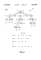
- FIG. 2 illustrates an example of a hierarchy of functions specified by the logic designer, as well as a net list of interconnections among the terminal functions of that hierarchy;
- FIG. 3 illustrates the basic system architecture of the preferred embodiment of this invention.
- FIGS. 4, 4A and 4B illustrate the detailed system architecture of the preferred embodiment of the invention.
- FIG. 1 illustrates a suitable hardware configuration of a workstation 10 in accordance with the present invention.
- the workstation 10 has a central processing unit 11, such as a conventional microprocessor, and a number of other units interconnected via a system bus 12.
- the illustrated workstation 10 shown in FIG. 1 includes a Random Access Memory (RAM) 13, a Read Only Memory (ROM) 14, an I/O adapter 15 for connecting peripheral devices such as disk units 16 to the bus 12, a user interface adapter 17 for connecting a keyboard 18, a mouse 19, a speaker 20, a microphone 21, and/or other user interface devices such as a touch screen device (not shown) to the bus 12.
- the workstation may also have a communications adapter 22 for connecting the workstation 10 to a data processing network 23 and a display adapter 24 for connecting the bus 12 to a display device 25.
- a preferred logic design program embodying the present invention may be supported on a computer workstation 10 with 24 megabytes of real memory and seventy-two megabytes of virtual memory.
- the workstation 10 employs the display device 25, keyboard 18, and mouse 19 to permit a user to interact with the various programs.
- a graphical editor is preferably utilized to draw schematics of each module or component that is desired.
- a workstation 10 which has given satisfactory results in practice has resident thereon the SUN SPARC desktop software which is a UNIX derivative as described in SUN's SPARCstation 1+ Installation Guide (1990), which is incorporated herein by reference.
- the LSI Modular Design Environment is also resident on the workstation and described in detail in the Network Design Language (NDL) reference published by LSI Logic Corporation (1987), which is incorporated herein by reference.
- NDL Network Design Language
- LPACE Planner and Chip Evaluator Program
- FIG. 2 illustrates an example of a logical hierarchy of functions 30 which this system might be asked to process.
- the CHIP 31 itself constitutes Level 1 of the hierarchy.
- the CHIP 31 has children, A, B, C, D and E, referred to with reference numerals 32, 33, 34, 35, and 36, respectively.
- Such children constitute Level 2 of the hierarchy.
- Level 3 contains: A1, A2 and A3, referred to with reference numerals 37, 38, and 39, respectively, which are the children of A 32; C1 and C2, referred to with reference numerals 40 and 41, respectively, which are the children of C 34; and, E1 and E2, referred to with reference numerals 42 and 43, respectively, which are the children of E 36.
- Level 4 contains: C11 and C12, referred to with reference numerals 44 and 45, respectively, which are the children of C1 40; and, E21 and E22, referred to with reference numerals 47 and 48, respectively, which are the children of E2 43.
- Level 5 contains C111 and C112, referred to with reference numerals 48 and 49, respectively, which are the children of C11.
- terminal functions exist not merely at the bottom of the hierarchy Level 5 (C111 48 and C112 49), but also at Level 2 (B 33 and D 35), Level 3 (A1 37, A2 38, A3 39, C2 41 and E1 42) and Level 4 (C12 45, E21 46 and E22 47).
- the NET LIST indicates the interconnections among such terminal functions.
- Net 1 indicates that functions A1 37, C111 48, E1 42 and E22 47 are interconnected, although it does not specify which pairs of such functions will actually be connected directly.
- the system embodying this invention estimates the expected number of connections between such functions, or functional blocks.
- Macrocell, macro function and megafunction components are accessible by entering the appropriate code. For instance, ":GET ,MACROFCN -- NAME.” is entered to retrieve a macro function with the desired name.
- the graphical editor employs drawing notations such as input, output, bi-directional, buses, bundles and extractor as a means of connecting functions.
- Commands can then be entered into the graphical editor to create a hierarchical level out of a selected group of objects or to remove a level of hierarchy from the design. Moreover, commands may be used to rearrange components to make the schematic more readable.
- Each hierarchical level has a symbol level and a corresponding network level.
- the top network level which is essentially the library menu, is viewed by the user.
- the user may define a function at the very top level and then place it at any level within the hierarchy. Alternatively, the user may define the function at the level of the hierarchy where it will be ultimately placed.
- a network list file (“.NETLIST”) of the design may be created.
- a design symbol and network may also be saved in a file called " ⁇ design>.def.”
- the error must be corrected or explained.
- a software flowchart of the logic system invention 50 is generally identified. After, an integrated circuit is described, the description is compiled through the LCMP 51 program. Thereafter, the compiled program is linked through the LLINK 52 program to yield the .SIM 53 file (a simulation file). The .SIM 53 file is then utilized as the input to the LVER 54 program (logic system verification program) to yield .DESIGN 55 and .PADREF 56 files. Thereafter, the .DESIGN 55 and .PADREF 56 files are employed as input to the Bonding Diagram program 57.
- the Bonding Diagram program 57 goes on to further create .BDCMD 58, a bonding diagram command file, as well as further edit the contents of the .BDCMD 58 file to establish the design's pin-to-pad connections. Using the edited .BDCMD 58 file as input, the Bonding Diagram program 57 is run again. Once the Bonding Diagram program 57 runs without any errors, a dump file termed .DMP 59 is created for each of the (n) integrated circuit chips within the design.
- a logic system .OPTSPEC 60 file is created which contains statements defining the maximum allowable delays and the maximum skew constraint for critical nets.
- the .OPTSPEC 60 file is then employed as input to the LDEL 61 program (logic system delay program). Using the RCI option, the LDEL 61 program is then run to create a .PROGBUF 62 and .RCI 63 file for each of the (n) integrated circuit chips within the design.
- the (n) .DMP 59 files, the (n) .RCI 63 files, and the (n) .PROGBUF 62 files are utilized as input to the LPACE 64 program to place the functional blocks of each integrated circuit.
- the LPACE 64 program is used to adjust the floorplan and recalculate delays until satisfied with the estimated delays.
- "SAVE" and "EXIT” the LPACE 64 program to generate (n) .CFUN 65 files, (n) .BLOCKS 66 files, and (n) .MODNET 67 files.
- Each of the files generated by the LPACE 64 are then inputted back to earlier used programs in order to update delays of any adjusted floorplan.
- the (n) .CFUN 65 files are used as input to the layout system, where, in turn, the layout system is used to input the LDEL 61 program, the (n) .BLOCKS 66 files are also inputted to the LDEL 61, whereas the (n) .CFUN 65 files are inputted into the LCMP 51 program.
- LDEL 61 program is rerun to update delay information for the adjusted floorplan.
- a detailed software flowchart of the logic system invention 50 is illustrated in six different phases.
- the LSED 70 program is employed to yield the .NET 71 file which is the user-created network description file.
- the .NET 71 file is then inputted into LCMP 51, a program that compiles network description files.
- the LCMP 51 program outputs both the .LCMPLIST 72 file and the .LIB 73 file.
- the .LCMPLIST 72 file is a diagnostic output file of LCMP 51
- the .LIB 73 file is a library file which contains the compiled version of the network.
- the .LIB 73 file is inputted into the LLINK 52 program along with the .TECHLIB 74 file which is formed from libraries of models for the chosen technology.
- the LLINK 52 program links the compiled .LIB 73 file with the .TECHLIB 74 file to yield the .LINKLST 75 file and the .SIM 53 file.
- the .SIM 53 file is then used to determine both delay prediction and design verification.
- the LVER 54 program performs electrical rule checking on the design and outputs six files from the input of the .SIM 53 file.
- the LVER 54 program verifies a network by checking: the number of gates used against the number of gates available; the number of pads used for power, ground and I/O against the number of available pads; cell-to-cell electrical connections for wiring feasibility; to ensure that high-level logic functions are used in valid hierarchical configurations; and, to ensure that high-level functions will fit on a selected die.
- the six output files of the LVER 54 program are .DESIGN 55, .PADREF 56, .XDELCEL 76, .DELCEL 77, .VERLST 78, and .IOD 79.
- the .DESIGN 55 file contains the network interconnects for layout.
- the .PADREF 56 and .IOD 79 files contain input/output data from logic simulation and input/output parametric data.
- the .VERLST 78 file contains network summary statistics. In conjunction with LDEL 61 program, the .DELCEL 77 and .XDELCEL 76 files are formed.
- the LBOND 80 program is utilized to define input/output connections between the package and the die (i.e., specify network pinout) and check for violations of mechanical and electrical packaging rules.
- the .PADREF 56, .DESIGN 55 and .IOD 79 files are inputted into the LBOND 80 program along with the .BDCMD 58 file.
- the .BDCMD 58 file is a user created file containing package pin-to-pad assignments.
- Six files are then generated by the LBOND 80 program: .BDTESTP/C 81, .BDLOGP/C 82, .IL3P/C 83, .SYSOUT 84, .PADREFP/C 85 and .DMP 89.
- the .BDTESTP/C 81 file is used in assembly whereas the .BDLOGP/C 82 file is used for troubleshooting results from the LBOND 80 program.
- the .IL3P/C 83 file is a plotting output file.
- the .PADREFP/C 85 file contains I/O pad information.
- a .DMP 59 file is generated for each of the (n) integrated circuit chips within the design. One of the purposes of the multiple .DMP 59 files is to preserve the region information should LBOND 80 terminate unexpectedly.
- the .PADREFP/C 85 and multiple .DMP 59 files are then combined to form the bonding diagram and inputted into the .WIRLEN 86 and .SEGLEN 87 files (of the LDEL 61 program which is run subsequently).
- the LDEL 61 program In the fourth phase, the LDEL 61 program generates the delay file for the simulation program.
- Four external files, the .SIM 53 file, the .BLOCKS 66 output file, the .WIRLEN 86 file, and the .SEGLEN 87 file are inputted into the LDEL 61 program.
- the four external files which are generated are termed .CPR 88, .SYSLOAD 89, .OPTSPEC 60, and .PATH 90.
- the .SYSLOAD 89 file specifies the output buffer loading information.
- the .OPTSPEC 60 file specifies optimization information for use in layout including critical net, programmable output buffers, clock net and bus lines, maximum skew time, and maximum margin.
- the .PATH 90 file allows the user to specify the critical path of the network.
- the .WIRLEN 86 file is a layout file containing exact metal wirelengths.
- the .SEGLEN 87 file is a layout file containing exact segment lengths of wires after layout.
- the LDEL 61 program outputs an updated simulation file, .SIMUPD 91, containing delay information as well as .DLYLST 92, .DELCEL 77, .XDELCEL 76, .XRFLST 93 and .CFRLST 94 files.
- the .DLYLST 92 file lists the user-specified payload information and default loading.
- the .DELCEL 77 and XDELCEL 76 files contain a list of all cells that were deleted since they were found to be unnecessary by the LDEL program.
- the .XRFLST 93 and .CRFLST 94 files are default outputs of the LDEL 61 program which cross-reference nets and cells.
- the LDEL 61 program generates both a .RCI 63 and .PROGBUF 62 file for each of the (n) integrated circuit chips within the design.
- Each .RC1 63 file contains critical signal or delay information to be used as inputs to the LPACE 64 program or layout.
- each .PROGBUF 62 file is employed as an output file for programmable buffers.
- LPACE 64 program performs hierarchical floorplanning and prepares wirelength information to allow a more accurate pre-layout delay prediction.
- the multiple .PROGBUF 62, .RC1 63 and .DMP 59 files are the inputs to the LPACE 64 program.
- Commands within the LPACE 64 program allow for a design of integrated circuit chips to be reconfigured by changing of block shapes, changing of block sizes, moving block positions, grouping of blocks together, display of interconnect density, display of delay violations and display of the relative sizes of blocks.
- the LPACE 64 program by itself, is capable of adjusting the floorplan and providing estimated delays. However, for exact delays to be determined, the LDEL 61 program must be regenerated.
- any minor logic changes made after running the LPACE 64 can be in evaluated through an interim design by running an abbreviated simulation sequence involving the LCMP 51, LLINK 52, LDEL 61, and LSIM 95 programs.
- the final design must, however, be evaluated more thoroughly by rerunning the LVER 54 program (to update the .DESIGN 55 and .PADREF 56 files) and the Bonding Diagram program 57 prior to obtaining sign-off on the final design.
- sets of (n) .BLOCKS 66, .CFUN 65 and .NETMOD files are then generated by the LPACE 64 program.
- Each .BLOCKS 66 file is then inputted into the LDEL 61 program for simulations.
- Each .CFUN 65 file is then inputted into the Layout System (with .DESIGN 55 and .PADREF 56 files from the LBOND 80 program).
- Each .NETMOD file, which are modified net files, is then inputted into the LCMP 51 program. The entire process is then redone to yield the final design.
Abstract
Description
Claims (16)
Priority Applications (1)
| Application Number | Priority Date | Filing Date | Title |
|---|---|---|---|
| US07/980,492 US5666289A (en) | 1992-10-07 | 1992-11-23 | Flexible design system |
Applications Claiming Priority (2)
| Application Number | Priority Date | Filing Date | Title |
|---|---|---|---|
| US95767292A | 1992-10-07 | 1992-10-07 | |
| US07/980,492 US5666289A (en) | 1992-10-07 | 1992-11-23 | Flexible design system |
Related Parent Applications (1)
| Application Number | Title | Priority Date | Filing Date |
|---|---|---|---|
| US95767292A Continuation-In-Part | 1992-10-07 | 1992-10-07 |
Publications (1)
| Publication Number | Publication Date |
|---|---|
| US5666289A true US5666289A (en) | 1997-09-09 |
Family
ID=25499947
Family Applications (1)
| Application Number | Title | Priority Date | Filing Date |
|---|---|---|---|
| US07/980,492 Expired - Lifetime US5666289A (en) | 1992-10-07 | 1992-11-23 | Flexible design system |
Country Status (1)
| Country | Link |
|---|---|
| US (1) | US5666289A (en) |
Cited By (29)
| Publication number | Priority date | Publication date | Assignee | Title |
|---|---|---|---|---|
| US5911061A (en) * | 1995-08-07 | 1999-06-08 | Hitachi, Ltd. | Program data creating method and apparatus for use with programmable devices in a logic emulation system |
| US5930811A (en) * | 1995-10-27 | 1999-07-27 | Fujitsu Limited | Document processing apparatus |
| US6247166B1 (en) * | 1998-06-25 | 2001-06-12 | International Business Machines Corporation | Method and apparatus for assembling array and datapath macros |
| US6249902B1 (en) * | 1998-01-09 | 2001-06-19 | Silicon Perspective Corporation | Design hierarchy-based placement |
| US6292925B1 (en) * | 1998-03-27 | 2001-09-18 | Xilinx, Inc. | Context-sensitive self implementing modules |
| US6367055B1 (en) * | 1999-04-27 | 2002-04-02 | Hewlett-Packard Company | Method and apparatus for determining certain characteristics of circuit elements |
| US6425109B1 (en) | 1999-07-23 | 2002-07-23 | International Business Machines Corporation | High level automatic core configuration |
| WO2002086771A1 (en) * | 2001-04-23 | 2002-10-31 | Telairity Semiconductor, Inc. | Circuit group design methodologies |
| US20020172210A1 (en) * | 2001-05-18 | 2002-11-21 | Gilbert Wolrich | Network device switch |
| US20030046641A1 (en) * | 2001-08-29 | 2003-03-06 | Fennell Timothy J. | Representing a simulation model using a hardware configuration database |
| US20030046053A1 (en) * | 2001-08-29 | 2003-03-06 | Wheeler William R. | Logic simulation |
| US20030046054A1 (en) * | 2001-08-29 | 2003-03-06 | Wheeler William R. | Providing modeling instrumentation with an application programming interface to a GUI application |
| US20030046051A1 (en) * | 2001-08-29 | 2003-03-06 | Wheeler William R. | Unified design parameter dependency management method and apparatus |
| US20030046052A1 (en) * | 2001-08-29 | 2003-03-06 | Wheeler William R. | Simulating a logic design |
| US20030135355A1 (en) * | 2002-01-17 | 2003-07-17 | Wheeler William R. | Modeling a logic design |
| US20030145311A1 (en) * | 2002-01-25 | 2003-07-31 | Wheeler William R. | Generating simulation code |
| US6640329B2 (en) | 2001-08-29 | 2003-10-28 | Intel Corporation | Real-time connection error checking method and process |
| US6643836B2 (en) | 2001-08-29 | 2003-11-04 | Intel Corporation | Displaying information relating to a logic design |
| US6662352B2 (en) | 2001-09-06 | 2003-12-09 | International Business Machines Corporation | Method of assigning chip I/O's to package channels |
| US6675139B1 (en) | 1999-03-16 | 2004-01-06 | Lsi Logic Corporation | Floor plan-based power bus analysis and design tool for integrated circuits |
| US6678873B1 (en) * | 1999-11-16 | 2004-01-13 | Matsushita Electric Industrial Co., Ltd. | Method of designing semiconductor integrated circuit device |
| US6704910B2 (en) * | 2001-07-24 | 2004-03-09 | Qualcore Logic, Inc. | Method for designing an integrated circuit containing multiple integrated circuit designs |
| US6708321B2 (en) | 2001-08-29 | 2004-03-16 | Intel Corporation | Generating a function within a logic design using a dialog box |
| US6721925B2 (en) | 2001-08-29 | 2004-04-13 | Intel Corporation | Employing intelligent logical models to enable concise logic representations for clarity of design description and for rapid design capture |
| US6983427B2 (en) | 2001-08-29 | 2006-01-03 | Intel Corporation | Generating a logic design |
| US7016794B2 (en) | 1999-03-16 | 2006-03-21 | Lsi Logic Corporation | Floor plan development electromigration and voltage drop analysis tool |
| US7073156B2 (en) * | 2001-08-29 | 2006-07-04 | Intel Corporation | Gate estimation process and method |
| US7093224B2 (en) | 2001-08-28 | 2006-08-15 | Intel Corporation | Model-based logic design |
| US8370791B2 (en) * | 2001-11-19 | 2013-02-05 | Cypress Semiconductor Corporation | System and method for performing next placements and pruning of disallowed placements for programming an integrated circuit |
Citations (6)
| Publication number | Priority date | Publication date | Assignee | Title |
|---|---|---|---|---|
| US4630219A (en) * | 1983-11-23 | 1986-12-16 | International Business Machines Corporation | Element placement method |
| US4636965A (en) * | 1984-05-10 | 1987-01-13 | Rca Corporation | Routing method in computer-aided-customization of universal arrays and resulting integrated circuit |
| US4918614A (en) * | 1987-06-02 | 1990-04-17 | Lsi Logic Corporation | Hierarchical floorplanner |
| US5309371A (en) * | 1989-06-28 | 1994-05-03 | Kawasaki Steel Corporation | Method of and apparatus for designing circuit block layout in integrated circuit |
| US5532934A (en) * | 1992-07-17 | 1996-07-02 | Lsi Logic Corporation | Floorplanning technique using multi-partitioning based on a partition cost factor for non-square shaped partitions |
| US5544067A (en) * | 1990-04-06 | 1996-08-06 | Lsi Logic Corporation | Method and system for creating, deriving and validating structural description of electronic system from higher level, behavior-oriented description, including interactive schematic design and simulation |
-
1992
- 1992-11-23 US US07/980,492 patent/US5666289A/en not_active Expired - Lifetime
Patent Citations (6)
| Publication number | Priority date | Publication date | Assignee | Title |
|---|---|---|---|---|
| US4630219A (en) * | 1983-11-23 | 1986-12-16 | International Business Machines Corporation | Element placement method |
| US4636965A (en) * | 1984-05-10 | 1987-01-13 | Rca Corporation | Routing method in computer-aided-customization of universal arrays and resulting integrated circuit |
| US4918614A (en) * | 1987-06-02 | 1990-04-17 | Lsi Logic Corporation | Hierarchical floorplanner |
| US5309371A (en) * | 1989-06-28 | 1994-05-03 | Kawasaki Steel Corporation | Method of and apparatus for designing circuit block layout in integrated circuit |
| US5544067A (en) * | 1990-04-06 | 1996-08-06 | Lsi Logic Corporation | Method and system for creating, deriving and validating structural description of electronic system from higher level, behavior-oriented description, including interactive schematic design and simulation |
| US5532934A (en) * | 1992-07-17 | 1996-07-02 | Lsi Logic Corporation | Floorplanning technique using multi-partitioning based on a partition cost factor for non-square shaped partitions |
Cited By (38)
| Publication number | Priority date | Publication date | Assignee | Title |
|---|---|---|---|---|
| US5911061A (en) * | 1995-08-07 | 1999-06-08 | Hitachi, Ltd. | Program data creating method and apparatus for use with programmable devices in a logic emulation system |
| US5930811A (en) * | 1995-10-27 | 1999-07-27 | Fujitsu Limited | Document processing apparatus |
| US6249902B1 (en) * | 1998-01-09 | 2001-06-19 | Silicon Perspective Corporation | Design hierarchy-based placement |
| US6292925B1 (en) * | 1998-03-27 | 2001-09-18 | Xilinx, Inc. | Context-sensitive self implementing modules |
| US6247166B1 (en) * | 1998-06-25 | 2001-06-12 | International Business Machines Corporation | Method and apparatus for assembling array and datapath macros |
| US6675139B1 (en) | 1999-03-16 | 2004-01-06 | Lsi Logic Corporation | Floor plan-based power bus analysis and design tool for integrated circuits |
| US7016794B2 (en) | 1999-03-16 | 2006-03-21 | Lsi Logic Corporation | Floor plan development electromigration and voltage drop analysis tool |
| US6367055B1 (en) * | 1999-04-27 | 2002-04-02 | Hewlett-Packard Company | Method and apparatus for determining certain characteristics of circuit elements |
| US6425109B1 (en) | 1999-07-23 | 2002-07-23 | International Business Machines Corporation | High level automatic core configuration |
| US6678873B1 (en) * | 1999-11-16 | 2004-01-13 | Matsushita Electric Industrial Co., Ltd. | Method of designing semiconductor integrated circuit device |
| US20050028128A1 (en) * | 2001-04-23 | 2005-02-03 | Telairity Semiconductor, Inc. | Circuit group design methodologies |
| WO2002086771A1 (en) * | 2001-04-23 | 2002-10-31 | Telairity Semiconductor, Inc. | Circuit group design methodologies |
| US7234123B2 (en) | 2001-04-23 | 2007-06-19 | Telairity Semiconductor, Inc. | Circuit group design methodologies |
| US20050022146A1 (en) * | 2001-04-23 | 2005-01-27 | Telairity Semiconductor, Inc. | Circuit group design methodologies |
| US6910199B2 (en) | 2001-04-23 | 2005-06-21 | Telairity Semiconductor, Inc. | Circuit group design methodologies |
| US20020172210A1 (en) * | 2001-05-18 | 2002-11-21 | Gilbert Wolrich | Network device switch |
| US7082104B2 (en) | 2001-05-18 | 2006-07-25 | Intel Corporation | Network device switch |
| US6704910B2 (en) * | 2001-07-24 | 2004-03-09 | Qualcore Logic, Inc. | Method for designing an integrated circuit containing multiple integrated circuit designs |
| US7093224B2 (en) | 2001-08-28 | 2006-08-15 | Intel Corporation | Model-based logic design |
| US20030046641A1 (en) * | 2001-08-29 | 2003-03-06 | Fennell Timothy J. | Representing a simulation model using a hardware configuration database |
| US6983427B2 (en) | 2001-08-29 | 2006-01-03 | Intel Corporation | Generating a logic design |
| US6643836B2 (en) | 2001-08-29 | 2003-11-04 | Intel Corporation | Displaying information relating to a logic design |
| US6708321B2 (en) | 2001-08-29 | 2004-03-16 | Intel Corporation | Generating a function within a logic design using a dialog box |
| US6721925B2 (en) | 2001-08-29 | 2004-04-13 | Intel Corporation | Employing intelligent logical models to enable concise logic representations for clarity of design description and for rapid design capture |
| US6640329B2 (en) | 2001-08-29 | 2003-10-28 | Intel Corporation | Real-time connection error checking method and process |
| US20030046053A1 (en) * | 2001-08-29 | 2003-03-06 | Wheeler William R. | Logic simulation |
| US6859913B2 (en) | 2001-08-29 | 2005-02-22 | Intel Corporation | Representing a simulation model using a hardware configuration database |
| US7130784B2 (en) | 2001-08-29 | 2006-10-31 | Intel Corporation | Logic simulation |
| US7107201B2 (en) | 2001-08-29 | 2006-09-12 | Intel Corporation | Simulating a logic design |
| US20030046052A1 (en) * | 2001-08-29 | 2003-03-06 | Wheeler William R. | Simulating a logic design |
| US7073156B2 (en) * | 2001-08-29 | 2006-07-04 | Intel Corporation | Gate estimation process and method |
| US20030046051A1 (en) * | 2001-08-29 | 2003-03-06 | Wheeler William R. | Unified design parameter dependency management method and apparatus |
| US20030046054A1 (en) * | 2001-08-29 | 2003-03-06 | Wheeler William R. | Providing modeling instrumentation with an application programming interface to a GUI application |
| US6662352B2 (en) | 2001-09-06 | 2003-12-09 | International Business Machines Corporation | Method of assigning chip I/O's to package channels |
| US8370791B2 (en) * | 2001-11-19 | 2013-02-05 | Cypress Semiconductor Corporation | System and method for performing next placements and pruning of disallowed placements for programming an integrated circuit |
| US20030135355A1 (en) * | 2002-01-17 | 2003-07-17 | Wheeler William R. | Modeling a logic design |
| US7197724B2 (en) | 2002-01-17 | 2007-03-27 | Intel Corporation | Modeling a logic design |
| US20030145311A1 (en) * | 2002-01-25 | 2003-07-31 | Wheeler William R. | Generating simulation code |
Similar Documents
| Publication | Publication Date | Title |
|---|---|---|
| US5666289A (en) | Flexible design system | |
| US6763506B1 (en) | Method of optimizing the design of electronic systems having multiple timing constraints | |
| US5612891A (en) | Hardware logic emulation system with memory capability | |
| US6480991B1 (en) | Timing-driven global placement based on geometry-aware timing budgets | |
| US5654898A (en) | Timing-driven integrated circuit layout through device sizing | |
| Das et al. | Design tools for 3-D integrated circuits | |
| US5553002A (en) | Method and system for creating and validating low level description of electronic design from higher level, behavior-oriented description, using milestone matrix incorporated into user-interface | |
| US5541849A (en) | Method and system for creating and validating low level description of electronic design from higher level, behavior-oriented description, including estimation and comparison of timing parameters | |
| US5880971A (en) | Methodology for deriving executable low-level structural descriptions and valid physical implementations of circuits and systems from semantic specifications and descriptions thereof | |
| US5572436A (en) | Method and system for creating and validating low level description of electronic design | |
| US5036473A (en) | Method of using electronically reconfigurable logic circuits | |
| US6249902B1 (en) | Design hierarchy-based placement | |
| US5930499A (en) | Method for mixed placement of structured and non-structured circuit elements | |
| US20050268258A1 (en) | Rule-based design consultant and method for integrated circuit design | |
| WO2000065490A1 (en) | Timing optimization in presence of interconnect delays | |
| Chen et al. | Simultaneous timing driven clustering and placement for FPGAs | |
| US7133819B1 (en) | Method for adaptive critical path delay estimation during timing-driven placement for hierarchical programmable logic devices | |
| US7171633B1 (en) | Estimating quality during early synthesis | |
| Gehring et al. | The trianus system and its application to custom computing | |
| US6968524B2 (en) | Method and apparatus to optimize an integrated circuit design using transistor folding | |
| US20060041852A1 (en) | Targeted optimization of buffer-tree logic | |
| US20040003363A1 (en) | Integrated circuit design and manufacture utilizing layers having a predetermined layout | |
| JP3193167B2 (en) | Logic synthesis system | |
| US6516453B1 (en) | Method for timing analysis during automatic scheduling of operations in the high-level synthesis of digital systems | |
| Chen et al. | Simultaneous placement with clustering and duplication |
Legal Events
| Date | Code | Title | Description |
|---|---|---|---|
| AS | Assignment |
Owner name: LSI LOGIC CORPORATION, CALIFORNIA Free format text: ASSIGNMENT OF ASSIGNORS INTEREST.;ASSIGNOR:WATKINS, DANIEL R.;REEL/FRAME:006351/0767 Effective date: 19921120 |
|
| STCF | Information on status: patent grant |
Free format text: PATENTED CASE |
|
| FPAY | Fee payment |
Year of fee payment: 4 |
|
| FPAY | Fee payment |
Year of fee payment: 8 |
|
| FEPP | Fee payment procedure |
Free format text: PAYOR NUMBER ASSIGNED (ORIGINAL EVENT CODE: ASPN); ENTITY STATUS OF PATENT OWNER: LARGE ENTITY Free format text: PAYER NUMBER DE-ASSIGNED (ORIGINAL EVENT CODE: RMPN); ENTITY STATUS OF PATENT OWNER: LARGE ENTITY |
|
| FPAY | Fee payment |
Year of fee payment: 12 |
|
| AS | Assignment |
Owner name: DEUTSCHE BANK AG NEW YORK BRANCH, AS COLLATERAL AG Free format text: PATENT SECURITY AGREEMENT;ASSIGNORS:LSI CORPORATION;AGERE SYSTEMS LLC;REEL/FRAME:032856/0031 Effective date: 20140506 |
|
| AS | Assignment |
Owner name: LSI CORPORATION, CALIFORNIA Free format text: CHANGE OF NAME;ASSIGNOR:LSI LOGIC CORPORATION;REEL/FRAME:033102/0270 Effective date: 20070406 |
|
| AS | Assignment |
Owner name: AVAGO TECHNOLOGIES GENERAL IP (SINGAPORE) PTE. LTD Free format text: ASSIGNMENT OF ASSIGNORS INTEREST;ASSIGNOR:LSI CORPORATION;REEL/FRAME:035390/0388 Effective date: 20140814 |
|
| AS | Assignment |
Owner name: AGERE SYSTEMS LLC, PENNSYLVANIA Free format text: TERMINATION AND RELEASE OF SECURITY INTEREST IN PATENT RIGHTS (RELEASES RF 032856-0031);ASSIGNOR:DEUTSCHE BANK AG NEW YORK BRANCH, AS COLLATERAL AGENT;REEL/FRAME:037684/0039 Effective date: 20160201 Owner name: LSI CORPORATION, CALIFORNIA Free format text: TERMINATION AND RELEASE OF SECURITY INTEREST IN PATENT RIGHTS (RELEASES RF 032856-0031);ASSIGNOR:DEUTSCHE BANK AG NEW YORK BRANCH, AS COLLATERAL AGENT;REEL/FRAME:037684/0039 Effective date: 20160201 |
|
| AS | Assignment |
Owner name: BELL SEMICONDUCTOR, LLC, ILLINOIS Free format text: ASSIGNMENT OF ASSIGNORS INTEREST;ASSIGNORS:AVAGO TECHNOLOGIES GENERAL IP (SINGAPORE) PTE. LTD.;BROADCOM CORPORATION;REEL/FRAME:044887/0109 Effective date: 20171208 |
|
| AS | Assignment |
Owner name: CORTLAND CAPITAL MARKET SERVICES LLC, AS COLLATERA Free format text: SECURITY INTEREST;ASSIGNORS:HILCO PATENT ACQUISITION 56, LLC;BELL SEMICONDUCTOR, LLC;BELL NORTHERN RESEARCH, LLC;REEL/FRAME:045216/0020 Effective date: 20180124 |
|
| AS | Assignment |
Owner name: BELL NORTHERN RESEARCH, LLC, ILLINOIS Free format text: RELEASE BY SECURED PARTY;ASSIGNOR:CORTLAND CAPITAL MARKET SERVICES LLC;REEL/FRAME:059720/0223 Effective date: 20220401 Owner name: BELL SEMICONDUCTOR, LLC, ILLINOIS Free format text: RELEASE BY SECURED PARTY;ASSIGNOR:CORTLAND CAPITAL MARKET SERVICES LLC;REEL/FRAME:059720/0223 Effective date: 20220401 Owner name: HILCO PATENT ACQUISITION 56, LLC, ILLINOIS Free format text: RELEASE BY SECURED PARTY;ASSIGNOR:CORTLAND CAPITAL MARKET SERVICES LLC;REEL/FRAME:059720/0223 Effective date: 20220401 |