US5670805A - Controlled recrystallization of buried strap in a semiconductor memory device - Google Patents
Controlled recrystallization of buried strap in a semiconductor memory device Download PDFInfo
- Publication number
- US5670805A US5670805A US08/643,983 US64398396A US5670805A US 5670805 A US5670805 A US 5670805A US 64398396 A US64398396 A US 64398396A US 5670805 A US5670805 A US 5670805A
- Authority
- US
- United States
- Prior art keywords
- trench
- buried strap
- semiconductor substrate
- capacitor
- oxide
- Prior art date
- Legal status (The legal status is an assumption and is not a legal conclusion. Google has not performed a legal analysis and makes no representation as to the accuracy of the status listed.)
- Expired - Lifetime
Links
Images


Classifications
-
- H—ELECTRICITY
- H10—SEMICONDUCTOR DEVICES; ELECTRIC SOLID-STATE DEVICES NOT OTHERWISE PROVIDED FOR
- H10B—ELECTRONIC MEMORY DEVICES
- H10B12/00—Dynamic random access memory [DRAM] devices
- H10B12/01—Manufacture or treatment
- H10B12/02—Manufacture or treatment for one transistor one-capacitor [1T-1C] memory cells
- H10B12/03—Making the capacitor or connections thereto
- H10B12/038—Making the capacitor or connections thereto the capacitor being in a trench in the substrate
Definitions
- the present invention generally relates to a method of manufacturing a semiconductor memory device and, more particularly, to a method of forming a buried strap for electrically connecting a storage trench capacitor to a transfer gate in a trench-capacitor type DRAM cell.
- FIG. 1 is a circuit diagram of a conventional memory cell 10 used in a dynamic random access memory (DRAM).
- Memory cell 10 includes a storage capacitor 15 for storing charges and a MOS transfer transistor (or "transfer gate") 20 for controlling charge transfer.
- MOS transfer transistor or "transfer gate”
- One end of the source-drain path of MOS transistor 20 is connected to bit line BL and the other end of the source-drain path of MOS transistor 20 is connected to a first electrode of capacitor 15.
- a second electrode of capacitor 15 is connected to a predetermined potential such as ground potential.
- the gate of MOS transistor 20 is connected to word line WL to which signals are applied for controlling the transfer of charges between storage capacitor 15 and bit line BL, thereby reading and writing data.
- FIGS. 2A and 2B illustrate the DRAM cell and buried strap described in the Nesbit et al. publication. Specifically, FIG. 2A illustrates a top-down view of a DRAM cell having a self-aligned buried strap and FIG. 2B is a cross-sectional view taken along line I-I' of FIG. 2A.
- DRAM cell 50 includes a trench capacitor 55 and a transfer gate 60.
- Trench capacitor 55 includes a first N+ polysilicon fill 65, a second N+ polysilicon fill 67, and a collar oxide 71.
- Transfer gate 60 includes N-type source/drain regions 73 and 74 formed in a P-well 75 and a polysilicon gate 77 insulatively spaced from the channel between source/drain regions 73 and 74.
- a bit line contact 79 electrically connects source/drain region 73 to bit line 81.
- a shallow trench isolation (STI) arrangement 80 electrically isolates DRAM cell 50 from an adjacent memory cell and passing word line 92.
- STI shallow trench isolation
- a diffusion region 83 is formed to electrically connect third polysilicon fill 69 and source/drain region 74 of MOS transfer gate 60 by outdiffusing dopants from the highly doped polysilicon fill in the storage trench into the P-well 75.
- Diffusion region 83 and third polysilicon fill 69 constitute a buried strap for connecting trench capacitor 55 to transfer gate 60.
- a first difficulty is that after the buried strap is formed, the thermal budget of the further semiconductor device fabrication process is limited. Exceeding this limit leads to an excessive outdiffusion from the trench polysilicon fill to underneath the transfer gate and towards neighboring memory cells. This dopant outdiffusion results in unacceptable changes of the transfer gate device characteristics as well as in possible electrical leakage between neighboring cells. With the shrinking design groundrule of high capacity DRAMs, the tolerable length of this outdiffusion also decreases. For example, in a 256 Mb Trench Capacitor DRAM cell with a 0.25 micrometer design groundrule and with the buried strap concept, only a 0.1 micrometer outdiffusion from the side of the trench is allowed.
- the limitation on the thermal budget after buried strap formation limits oxidation steps to low temperature and conflicts with the need for thermal anneals to heal implantation damage or to relieve stress built up in the silicon substrate during the fabrication process.
- oxygen can diffuse from the substrate surface into the collar oxide and oxidize the sidewalls of the polysilicon trench fill and the substrate as shown in FIG. 3.
- the collar oxide expands and forms a vertical bird's-beak-shape. This collar expansion leads to a high stress level and to generation of extended crystal defects in the substrate like dislocations and stacking faults around the most expanded part of the oxide collar. Extended crystal defects can cause electrical leakage across junctions.
- Another difficulty related to the buried strap concept is the generation of extended crystal defects at the interface of polycrystalline trench fill 69 to the crystalline silicon substrate. This interface sits next to the area where the oxide collar expands most during the oxidation steps of the fabrication process and therefore is exposed to the highest stress field.
- the polysilicon trench fill 69 contacting the single-crystalline silicon substrate starts to recrystallize in an uncontrolled manner over a distance which can be as far as the width of the collar oxide.
- crystal defects in the polysilicon grains (twins, stacking faults, etc.) act as seeds for defect formation at the interface to the neighboring substrate. Crystal defects are generated there and pushed far into the substrate.
- a method of forming a coupled capacitor and transistor is provided.
- a trench is formed in a semiconductor substrate and an impurity-doped first conductive region is then formed by filling the trench with an impurity-doped first conductive material.
- the impurity-doped first conductive region is etched back to a first level within the trench.
- An insulating layer is then formed on a sidewall of the potion of the trench opened by the etching back of the impurity-doped first conductive region and a second conductive region is formed by filling the remainder of the trench with a second conductive material.
- the insulating layer and the second conductive region are etched back to a second level within the trench and an undoped amorphous silicon layer is formed in the potion of the trench opened by the etching back of the insulating layer and the second conductive region.
- the undoped amorphous silicon layer is etched back to a third level within the trench.
- the undoped amorphous silicon layer is then recrystallized. Impurities are subsequently outdiffused from the impurity-doped first conductive region to the semiconductor substrate through the recrystallized silicon layer.
- a source/drain region of the transistor is formed adjacent to an intersection of the trench and the surface of the semiconductor substrate.
- the outdiffused impurities and the recrystallized silicon layer constitute a buried strap for electrically connecting the first and second conductive layers in the trench to the source/drain region.
- an additional thermal budget of, for example, at least 90 minutes at 1050° Celsius is achieved.
- This additional thermal budget can be used for appropriate stress relief anneals without resulting in any excessive dopant outdiffusion from the trench.
- the interface of the polysilicon and the single crystal silicon is moved away or recessed from the high stress area around the expanded collar oxide. This avoids the generation and extension of crystal defects into the semiconductor substrate.
- FIG. 1 is a circuit diagram of a conventional DRAM memory cell.
- FIGS. 2A and 2B are top-down and cross-sectional views, respectively, of a DRAM cell with a self-aligned buried strap.
- FIG. 3 illustrates the expansion of collar oxide 71 due to oxidation processes after buried strap formation.
- FIGS. 4A-4H illustrate the method of forming a semiconductor device in accordance with the present invention.
- FIG. 5 is a detailed illustration of the recrystallization of undoped amorphous silicon layer 107.
- FIGS. 6A and 6B illustrate defects which are constrained in the trench fill and which extend into the semiconductor substrate, respectively.
- FIGS. 7A and 7B respectively illustrate buried straps formed in accordance with the method of the present invention and in accordance with a prior art method, respectively.
- a buried N-type well 100 is formed in a P - -type semiconductor substrate 10 by implanting phosphorous below the intended P-well for a memory cell array.
- a buried N-type well may also be formed by other methods, e.g., P-well implantation into an N-type semiconductor substrate or by epitaxy, and the invention is not limited in this respect.
- a silicon nitride layer 102 of about 0.2 micrometers is formed by chemical vapor deposition, for example, on the surface of a thin oxide layer 101 (e.g., about 10 nanometers) which is thermally grown on semiconductor substrate 10.
- Oxide layer 101 and silicon nitride layer 102 are patterned and etched to provide a mask for etching a trench 103.
- Trench 103 is etched using an anisotropic etching process to a depth of about 8 micrometers as shown in FIG. 4B.
- an N + -type capacitor plate 104 is formed by outdiffusing arsenic from the lower portion of trench 103.
- An oxidized nitride (ON) storage node dielectric (not shown) is then formed in trench 103. After the dielectric is formed, a first conductive region is formed by filling trench 103 with an impurity-doped first conductive material such as N + -type polycrystalline silicon.
- the filling step may be carried out using chemical vapor deposition of silane or disilane, for example.
- the N + -type polycrystalline silicon is then etched back to a first level within trench 103 using an isotropic etch process to form a first trench fill 105.
- the level of first trench fill 104 is about 1.0 micrometer below the surface of semiconductor substrate 10.
- a collar oxide 106 is then formed on the sidewall of the portion of trench 103 opened by the etching back of the N + -type polycrystalline silicon using LPCVD or PECVD TEOS as shown in FIG. 4C.
- a second conductive region is formed by filling in the remainder of trench 103 with a second conductive material.
- the second conductive material may be, for example, N + -type polycrystalline silicon or undoped polycrystalline silicon and may be formed by chemical vapor deposition.
- the second conductive material and the oxide collar 106 are then etched back to a second level within trench 103 to form a second trench fill 107 insulated from the semiconductor substrate by oxide collar 106 as shown in FIG. 4D.
- the depth of the buried strap to be formed in a subsequent process step is defined by this controlled etch-back of the second conductive material and oxide collar 106.
- Second trench fill 107 is etched back to about 0.1 micrometer below the surface of semiconductor substrate 10.
- An in-situ removal of a native oxide in trench 103 is then performed.
- a native oxide on the upper surface of second trench fill 106 and on the sidewall of trench 103 through which impurities for the buried strap will subsequently be outdiffused are removed.
- This removal of native oxide may be carried out by an in-situ prebake in a hydrogen ambient at a temperature greater than 850° Celsius, for example.
- the portion of trench 103 opened by the etching back of oxide collar 105 and the second conductive material is then filled by amorphously depositing undoped silicon using chemical vapor deposition, for example.
- the amorphous silicon may be doped, this silicon will act as a diffusion barrier for dopants in the deep trench fill as will be explained below and is more effective in performing this function if undoped.
- the undoped amorphous silicon is then etched back using reactive ion etching, for example, to form a third trench fill 108 as shown in FIG. 4E.
- the amorphous silicon is preferably etched back to about 0.05 micrometer below the surface of semiconductor substrate 10 as determined by the tolerable resistance of the buried strap, and by the recess etch controllability.
- third trench fill 108 can be accomplished in a controlled manner if the undoped silicon is deposited amorphously.
- a reactive ion etch is performed to provide shallow trench 110 for shallow trench isolation.
- shallow trench isolation is used to isolate discrete memory cell devices to prevent interference therebetween.
- a shallow trench such as shallow trench 110 is formed between adjacent deep trench configurations to ensure that they operate independently.
- the undoped amorphous silicon layer 108 is recrystallized as shown in FIG. 4G and in more detail in FIG. 5.
- the recrystallization is performed by heating at a temperature at which the amorphous silicon layer 108 begins to recrystallize, but at which the spontaneous formation of polysilicon is still prevented.
- a typical recrystallization temperature is around 550° C. and a typical temperature range for recrystallization is between about 500° and 700° C.
- the recrystallization rate of amorphous silicon depends exponentially on temperature: the lower the temperature, the longer the process time.
- the extension of the recrystallized area is determined by the depth of the amorphous silicon layer 108. Because recrystallization simultaneously starts at the interface of amorphous silicon layer 108 and the substrate and at the interface of second conductive region 107 and amorphous silicon layer 108, a single crystalline area without any defects will be formed in the hatched area of FIG. 5.
- the dotted area in FIG. 5 contains polycrystalline grains. The diagonal line in between these two areas indicates the interface at which the recrystallizing front and the polysilicon front meet.
- the crystalline silicon substrate acts as a seed for the recrystallization, a native oxide in between the substrate and the amorphous silicon layer 108 as well as a native oxide in between second conductive region 107 and amorphous silicon layer 108 is not acceptable. Therefore the in-situ removal of the native oxide prior to deposition of the amorphous silicon as described above is important.
- the recrystallization step can be easily integrated in the fabrication process if, for example, prior to a subsequent shallow trench isolation (STI) oxidation step, wafers are placed in a furnace at, for example, 550° C. and kept at this temperature under nitrogen ambient for some minutes (e.g., 10 minutes). As noted above, recrystallization time depends exponentially on temperature. The recrystallization time is also dependent on the quality of the amorphously deposited silicon.
- STI shallow trench isolation
- Shallow trench 110 is then filled in to ensure isolation from adjacent trench structures.
- an oxide lining 120 may be formed over the layer 107 and the interior surface of shallow trench 110.
- a nitride lining 122 may then be formed over oxide lining 120.
- the oxide and nitride linings 120, 122 serve to isolate collar oxide 105 from oxidant, and thereby suppress dislocation and stress.
- shallow trench 110 may be filled according to techniques known in the art. For example, an oxide 124 may be deposited to fill in shallow trench 110.
- stress relief anneals can be performed without the outdiffusion affecting the transfer gate characteristics or adjacent memory cells.
- stress relief anneals are preferably carried out after oxidation steps which generate stress in the substrate (e.g., sacrificial gate oxide, gate oxide), or after ion implantation.
- the substrate e.g., sacrificial gate oxide, gate oxide
- the generation and extension of crystal defects into the substrate is reduced.
- a gate insulator may then be formed on the planar surface, and gate material may be deposited and patterned to form gate electrodes. Using the gate electrodes as masks, source/drain regions may be formed by ion implantation. Accordingly, transfer gates coupled to trench capacitors are realized. Interconnection between devices and metallization to the output terminals are conducted using techniques known in the art.
- a simple, process-compatible method for fabricating a diffusion-limiting interconnection between the polysilicon fill of a deep trench capacitor and the semiconductor substrate before a buried strap is outdiffused.
- This interconnection consists of undoped crystalline silicon of a defined width which has been formed by a controlled recrystallization of the upper part of the deep trench fill. An additional thermal budget is then given to allow proper stress relief anneals in the fabrication process of DRAM cells with deep trench and buried strap.
- the controlled recrystallization of the upper part of the trench fill recesses the single/poly-crystalline interface behind the expanded collar oxide, thereby avoiding the generation and extension of crystal defects into the substrate, while simultaneously solving the problem of the limited thermal budget.
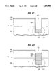
- the additional thermal budget gained by the buried strap recrystallization can be seen from FIGS. 7A and 7B.
- the outdiffusion of the buried strap is simulated for two cases.
- the first trench fill is assumed to be doped with (As) 5 ⁇ 10 19 cm -2 and the second and third trench fills are assumed to be undoped.
- the p-well doping around the trench is (B) 2 ⁇ 10 17 cm -2 .
- FIG. 7A shows a trench with a recrystallized buried strap.
- the simulation is based upon the thermal budget for the fabrication process (which does not include any stress relief anneals) plus an additional thermal budget for stress relief of, for example, 90 minutes at 1050° C.
- 90 minutes at 1050° is merely exemplary of the additional thermal budget which may be gained in accordance with this invention.
- the outdiffused buried strap overlaps the source/drain region so that good contact is guaranteed.
- the junction width of the buried strap to the P-well is below 0.1 micrometer so that there is no effect on the transfer device characteristics. Further, there is no chance of electrical leakage to the buried strap of neighboring cells.
- FIG. 7B shows an identical structure, simulated with the same thermal budget as in FIG. 7A, but without buried strap recrystallization.
- the buried strap outdiffusion of about 0.15 micrometers may already influence the transfer device characteristics.
- a perfect overlay alignment of the transfer gate to the trenches is assumed.
- the outdiffused buried strap reaches underneath the transfer gate.
- the electrical characteristics of the transfer device will be strongly affected. Also the possibility of cell-to-cell leakage via buried straps of neighboring cells is much higher than in the case without buried strap recrystallization.
- the simulations show clearly that with the buried strap recrystallization, a much higher thermal budget of the fabrication process is allowed.
- the additional thermal budget of, for example, at least 90 minutes at 1050° C. which is gained by the controlled recrystallization of the third trench fill, can be used for appropriate stress relief anneals without any excessive dopant outdiffusion from the trench.
Abstract
Description
Claims (1)
Priority Applications (1)
| Application Number | Priority Date | Filing Date | Title |
|---|---|---|---|
| US08/643,983 US5670805A (en) | 1995-03-29 | 1996-05-07 | Controlled recrystallization of buried strap in a semiconductor memory device |
Applications Claiming Priority (2)
| Application Number | Priority Date | Filing Date | Title |
|---|---|---|---|
| US08/412,442 US5543348A (en) | 1995-03-29 | 1995-03-29 | Controlled recrystallization of buried strap in a semiconductor memory device |
| US08/643,983 US5670805A (en) | 1995-03-29 | 1996-05-07 | Controlled recrystallization of buried strap in a semiconductor memory device |
Related Parent Applications (1)
| Application Number | Title | Priority Date | Filing Date |
|---|---|---|---|
| US08/412,442 Division US5543348A (en) | 1995-03-29 | 1995-03-29 | Controlled recrystallization of buried strap in a semiconductor memory device |
Publications (1)
| Publication Number | Publication Date |
|---|---|
| US5670805A true US5670805A (en) | 1997-09-23 |
Family
ID=23632996
Family Applications (2)
| Application Number | Title | Priority Date | Filing Date |
|---|---|---|---|
| US08/412,442 Expired - Lifetime US5543348A (en) | 1995-03-29 | 1995-03-29 | Controlled recrystallization of buried strap in a semiconductor memory device |
| US08/643,983 Expired - Lifetime US5670805A (en) | 1995-03-29 | 1996-05-07 | Controlled recrystallization of buried strap in a semiconductor memory device |
Family Applications Before (1)
| Application Number | Title | Priority Date | Filing Date |
|---|---|---|---|
| US08/412,442 Expired - Lifetime US5543348A (en) | 1995-03-29 | 1995-03-29 | Controlled recrystallization of buried strap in a semiconductor memory device |
Country Status (5)
| Country | Link |
|---|---|
| US (2) | US5543348A (en) |
| EP (1) | EP0739033A3 (en) |
| JP (1) | JP3078223B2 (en) |
| KR (1) | KR100202278B1 (en) |
| TW (1) | TW290724B (en) |
Cited By (36)
| Publication number | Priority date | Publication date | Assignee | Title |
|---|---|---|---|---|
| US5909044A (en) * | 1997-07-18 | 1999-06-01 | International Business Machines Corporation | Process for forming a high density semiconductor device |
| EP0962972A1 (en) * | 1998-06-02 | 1999-12-08 | International Business Machines Corporation | DRAM trench capacitor and method of fabricating the same |
| EP0971414A1 (en) * | 1998-06-15 | 2000-01-12 | Siemens Aktiengesellschaft | Trench capacitor with insulating collar and buried contact and corresponding manufacturing process |
| US6066566A (en) * | 1998-01-28 | 2000-05-23 | International Business Machines Corporation | High selectivity collar oxide etch processes |
| WO2000055905A1 (en) * | 1999-03-12 | 2000-09-21 | Infineon Technologies Ag | Method for producing a dram structure with buried bit lines or trench capacitors |
| US6140675A (en) * | 1998-08-06 | 2000-10-31 | Kabushiki Kaisha Toshiba | Semiconductor device and manufacturing method thereof |
| US6140175A (en) * | 1999-03-03 | 2000-10-31 | International Business Machines Corporation | Self-aligned deep trench DRAM array device |
| US6150670A (en) * | 1999-11-30 | 2000-11-21 | International Business Machines Corporation | Process for fabricating a uniform gate oxide of a vertical transistor |
| EP1039534A3 (en) * | 1999-03-24 | 2001-04-04 | Infineon Technologies North America Corp. | Dynamic random access memory |
| US6229173B1 (en) * | 1999-06-23 | 2001-05-08 | International Business Machines Corporation | Hybrid 5F2 cell layout for buried surface strap aligned to vertical transistor |
| US6326658B1 (en) | 1998-09-25 | 2001-12-04 | Kabushiki Kaisha Toshiba | Semiconductor device including an interface layer containing chlorine |
| US6328794B1 (en) * | 1993-06-26 | 2001-12-11 | International Business Machines Corporation | Method of controlling stress in a film |
| US6333531B1 (en) | 1999-01-29 | 2001-12-25 | International Business Machines Corporation | Dopant control of semiconductor devices |
| US6339228B1 (en) * | 1999-10-27 | 2002-01-15 | International Business Machines Corporation | DRAM cell buried strap leakage measurement structure and method |
| US6365512B1 (en) | 2000-06-21 | 2002-04-02 | Infineon Technologies Ag | Method and apparatus for a direct buried strap for same level contact interconnections for semiconductor devices |
| US6369419B1 (en) | 2000-06-23 | 2002-04-09 | International Business Machines Corporation | Self-aligned near surface strap for high density trench DRAMS |
| US6372573B2 (en) | 1999-10-26 | 2002-04-16 | Kabushiki Kaisha Toshiba | Self-aligned trench capacitor capping process for high density DRAM cells |
| US6380575B1 (en) | 1999-08-31 | 2002-04-30 | International Business Machines Corporation | DRAM trench cell |
| US6417063B1 (en) | 2000-06-22 | 2002-07-09 | Infineon Technologies Richmond, Lp | Folded deep trench capacitor and method |
| US6440794B1 (en) | 1999-05-28 | 2002-08-27 | International Business Machines Corporation | Method for forming an array of DRAM cells by employing a self-aligned adjacent node isolation technique |
| KR100360735B1 (en) * | 1999-05-13 | 2002-11-13 | 인터내셔널 비지네스 머신즈 코포레이션 | Formation of 5f2 cell with partially vertical transistor and gate conductor aligned buried strap with raised shallow trench isolation region |
| US6501117B1 (en) * | 2001-11-05 | 2002-12-31 | International Business Machines Corporation | Static self-refreshing DRAM structure and operating mode |
| US6503798B1 (en) | 2000-06-30 | 2003-01-07 | International Business Machines Corporation | Low resistance strap for high density trench DRAMS |
| US6518118B2 (en) | 2001-03-15 | 2003-02-11 | International Business Machines Corporation | Structure and process for buried bitline and single sided buried conductor formation |
| US20030148575A1 (en) * | 2000-12-19 | 2003-08-07 | Micron Technology, Inc. | Methods of accessing floating-gate memory cells having underlying source-line connections |
| US20030162352A1 (en) * | 2002-02-28 | 2003-08-28 | Arkalgud Sitaram | Method for fabricating a memory cell |
| US20030203587A1 (en) * | 2001-12-10 | 2003-10-30 | Oleg Gluschenkov | Vertical thermal nitride mask (anti-collar) and processing thereof |
| US6653678B2 (en) * | 2001-07-13 | 2003-11-25 | International Business Machines Corporation | Reduction of polysilicon stress in trench capacitors |
| US20040063277A1 (en) * | 2002-09-27 | 2004-04-01 | International Business Machines Corporation | Semiconductor method and structure for simultaneously forming a trench capacitor dielectric and trench sidewall device dielectric |
| US6828192B2 (en) | 2001-03-09 | 2004-12-07 | Infineon Technologies Ag | Semiconductor memory cell and method for fabricating the memory cell |
| US6828191B1 (en) | 1998-06-15 | 2004-12-07 | Siemens Aktiengesellschaft | Trench capacitor with an insulation collar and method for producing a trench capacitor |
| US20050026384A1 (en) * | 2003-07-29 | 2005-02-03 | Infineon Technologies Ag | Method for fabricating trench capacitor with insulation collar electrically connected to substrate through buried contact, in particular, for a semiconductor memory cell |
| US20060216889A1 (en) * | 2005-03-28 | 2006-09-28 | Promos Technologies Inc. | Memories having a charge storage node at least partially located in a trench in a semiconductor substrate and electrically coupled to a source/drain region formed in the substrate |
| US20070077702A1 (en) * | 2005-05-19 | 2007-04-05 | International Business Machines Corporation | Trench memory cell and method for making the same |
| US8318574B2 (en) | 2010-07-30 | 2012-11-27 | International Business Machines Corporation | SOI trench DRAM structure with backside strap |
| US8492811B2 (en) | 2010-09-20 | 2013-07-23 | International Business Machines Corporation | Self-aligned strap for embedded capacitor and replacement gate devices |
Families Citing this family (29)
| Publication number | Priority date | Publication date | Assignee | Title |
|---|---|---|---|---|
| US5827765A (en) * | 1996-02-22 | 1998-10-27 | Siemens Aktiengesellschaft | Buried-strap formation in a dram trench capacitor |
| US5939333A (en) * | 1996-05-30 | 1999-08-17 | Micron Technology, Inc. | Silicon nitride deposition method |
| KR100269289B1 (en) * | 1997-02-19 | 2000-10-16 | 윤종용 | Method for crystallizing a silicon film |
| US6025224A (en) * | 1997-03-31 | 2000-02-15 | Siemens Aktiengesellschaft | Device with asymmetrical channel dopant profile |
| JP3132435B2 (en) | 1997-09-22 | 2001-02-05 | 日本電気株式会社 | Method for manufacturing semiconductor device |
| US5981332A (en) * | 1997-09-30 | 1999-11-09 | Siemens Aktiengesellschaft | Reduced parasitic leakage in semiconductor devices |
| US5990511A (en) * | 1997-10-16 | 1999-11-23 | International Business Machines Corporation | Memory cell with transfer device node in selective polysilicon |
| US5963814A (en) * | 1997-10-28 | 1999-10-05 | Micron Technology, Inc. | Method of forming recessed container cells by wet etching conductive layer and dissimilar layer formed over conductive layer |
| US6583457B1 (en) | 1997-10-28 | 2003-06-24 | Micron Technology, Inc. | Recessed container cells and method of forming the same |
| DE19752968C1 (en) * | 1997-11-28 | 1999-06-24 | Siemens Ag | Memory cell arrangement and method for its production |
| US6110792A (en) * | 1998-08-19 | 2000-08-29 | International Business Machines Corporation | Method for making DRAM capacitor strap |
| GB2341483B (en) * | 1998-09-11 | 2003-10-01 | Siemens Plc | Improved process for dram cell production |
| US6222218B1 (en) * | 1998-09-14 | 2001-04-24 | International Business Machines Corporation | DRAM trench |
| DE19843641A1 (en) * | 1998-09-23 | 2000-04-20 | Siemens Ag | Trench capacitor with insulation collar and corresponding manufacturing process |
| US6194736B1 (en) * | 1998-12-17 | 2001-02-27 | International Business Machines Corporation | Quantum conductive recrystallization barrier layers |
| US6331459B1 (en) * | 1999-02-18 | 2001-12-18 | Infineon Technologies Ag | Use of dummy poly spacers and divot fill techniques for DT-aligned processing after STI formation for advanced deep trench capacitor DRAM |
| TW483152B (en) * | 1999-07-01 | 2002-04-11 | Ibm | Improved methods of forming the buried strap and its quantum barrier in deep trench cell capacitors |
| US6320215B1 (en) * | 1999-07-22 | 2001-11-20 | International Business Machines Corporation | Crystal-axis-aligned vertical side wall device |
| DE19944011B4 (en) * | 1999-09-14 | 2007-10-18 | Infineon Technologies Ag | Method for forming at least two memory cells of a semiconductor memory |
| DE19957123B4 (en) * | 1999-11-26 | 2006-11-16 | Infineon Technologies Ag | Method for producing a cell arrangement for a dynamic semiconductor memory |
| FR2819637B1 (en) * | 2001-01-12 | 2003-05-30 | St Microelectronics Sa | INTEGRATED CIRCUIT COMPRISING A PHOTODIODE-TYPE SEMICONDUCTOR DEVICE, AND MANUFACTURING METHOD |
| FR2819636B1 (en) * | 2001-01-12 | 2003-09-26 | St Microelectronics Sa | INTEGRATED CIRCUIT INCLUDING A DRAM TYPE MEMORY POINT, AND MANUFACTURING PROCESS |
| TW507365B (en) * | 2001-03-09 | 2002-10-21 | Nanya Technology Corp | Method for treating surface of sidewall of deep trench |
| US6624031B2 (en) * | 2001-11-20 | 2003-09-23 | International Business Machines Corporation | Test structure and methodology for semiconductor stress-induced defects and antifuse based on same test structure |
| DE10210434B4 (en) * | 2002-03-09 | 2007-12-27 | Infineon Technologies Ag | A method for generating a shallow trench isolation in a semiconductor device and use of such a method |
| US6620677B1 (en) * | 2002-05-31 | 2003-09-16 | Infineon Technologies Ag | Support liner for isolation trench height control in vertical DRAM processing |
| US6635526B1 (en) | 2002-06-07 | 2003-10-21 | Infineon Technologies Ag | Structure and method for dual work function logic devices in vertical DRAM process |
| TW587305B (en) * | 2003-05-30 | 2004-05-11 | Nanya Technology Corp | A method for controlling the upper width of a trench |
| TW200820433A (en) * | 2006-10-23 | 2008-05-01 | Promos Technologies Inc | Method for preparing a trench capacitor structure |
Citations (25)
| Publication number | Priority date | Publication date | Assignee | Title |
|---|---|---|---|---|
| US4444620A (en) * | 1983-09-12 | 1984-04-24 | Bell Telephone Laboratories, Incorporated | Growth of oriented single crystal semiconductor on insulator |
| US4509990A (en) * | 1982-11-15 | 1985-04-09 | Hughes Aircraft Company | Solid phase epitaxy and regrowth process with controlled defect density profiling for heteroepitaxial semiconductor on insulator composite substrates |
| US4584025A (en) * | 1983-11-30 | 1986-04-22 | Fujitsu Limited | Process for fabricating a semiconductor on insulator semiconductor device |
| US4659392A (en) * | 1985-03-21 | 1987-04-21 | Hughes Aircraft Company | Selective area double epitaxial process for fabricating silicon-on-insulator structures for use with MOS devices and integrated circuits |
| US4716548A (en) * | 1985-02-13 | 1987-12-29 | Kabushiki Kaisha Toshiba | Semiconductor memory cell |
| US4753895A (en) * | 1987-02-24 | 1988-06-28 | Hughes Aircraft Company | Method of forming low leakage CMOS device on insulating substrate |
| US4816893A (en) * | 1987-02-24 | 1989-03-28 | Hughes Aircraft Company | Low leakage CMOS/insulator substrate devices and method of forming the same |
| US4820652A (en) * | 1985-12-11 | 1989-04-11 | Sony Corporation | Manufacturing process and structure of semiconductor memory devices |
| US4824793A (en) * | 1984-09-27 | 1989-04-25 | Texas Instruments Incorporated | Method of making DRAM cell with trench capacitor |
| US4826300A (en) * | 1987-07-30 | 1989-05-02 | Hughes Aircraft Company | Silicon-on-sapphire liquid crystal light valve and method |
| US4849371A (en) * | 1986-12-22 | 1989-07-18 | Motorola Inc. | Monocrystalline semiconductor buried layers for electrical contacts to semiconductor devices |
| US4853342A (en) * | 1987-08-14 | 1989-08-01 | Kabushiki Kaisha Toshiba | Method of manufacturing semiconductor integrated circuit device having transistor |
| US4910709A (en) * | 1988-08-10 | 1990-03-20 | International Business Machines Corporation | Complementary metal-oxide-semiconductor transistor and one-capacitor dynamic-random-access memory cell |
| US4916524A (en) * | 1987-03-16 | 1990-04-10 | Texas Instruments Incorporated | Dram cell and method |
| US4915746A (en) * | 1988-08-15 | 1990-04-10 | Welsch Gerhard E | Method of forming high temperature barriers in structural metals to make such metals creep resistant at high homologous temperatures |
| US4942554A (en) * | 1987-11-26 | 1990-07-17 | Siemens Aktiengesellschaft | Three-dimensional, one-transistor cell arrangement for dynamic semiconductor memories comprising trench capacitor and method for manufacturing same |
| US4988637A (en) * | 1990-06-29 | 1991-01-29 | International Business Machines Corp. | Method for fabricating a mesa transistor-trench capacitor memory cell structure |
| US5116768A (en) * | 1989-03-20 | 1992-05-26 | Fujitsu Limited | Fabrication method of a semiconductor integrated circuit having an SOI device and a bulk semiconductor device on a common semiconductor substrate |
| US5138420A (en) * | 1989-11-24 | 1992-08-11 | Mitsubishi Denki Kabushiki Kaisha | Semiconductor device having first and second type field effect transistors separated by a barrier |
| US5168366A (en) * | 1987-01-27 | 1992-12-01 | Oki Electric Industry Co., Ltd. | Dynamic semiconductor memory device comprising a switching transistor and storage capacitor |
| US5185294A (en) * | 1991-11-22 | 1993-02-09 | International Business Machines Corporation | Boron out-diffused surface strap process |
| US5292678A (en) * | 1991-11-04 | 1994-03-08 | International Business Machines Corporation | Forming a bit line configuration for semiconductor memory |
| US5308783A (en) * | 1992-12-16 | 1994-05-03 | Siemens Aktiengesellschaft | Process for the manufacture of a high density cell array of gain memory cells |
| US5336629A (en) * | 1991-08-05 | 1994-08-09 | International Business Machines Corporation | Folder Bitline DRAM having access transistors stacked above trench storage capacitors, each such transistor employing a planar semiconductor body which spans adjacent capacitors |
| US5360758A (en) * | 1993-12-03 | 1994-11-01 | International Business Machines Corporation | Self-aligned buried strap for trench type DRAM cells |
Family Cites Families (11)
| Publication number | Priority date | Publication date | Assignee | Title |
|---|---|---|---|---|
| EP0283964B1 (en) * | 1987-03-20 | 1994-09-28 | Nec Corporation | Dynamic random access memory device having a plurality of improved one-transistor type memory cells |
| US5168073A (en) * | 1991-10-31 | 1992-12-01 | Micron Technology, Inc. | Method for fabricating storage node capacitor having tungsten and etched tin storage node capacitor plate |
| US5192703A (en) * | 1991-10-31 | 1993-03-09 | Micron Technology, Inc. | Method of making tungsten contact core stack capacitor |
| US5262662A (en) * | 1991-10-31 | 1993-11-16 | Micron Technology, Inc. | Storage node capacitor having tungsten and etched tin storage node capacitor plate |
| JPH0799771B2 (en) * | 1992-06-26 | 1995-10-25 | インターナショナル・ビジネス・マシーンズ・コーポレイション | Method of controlling stress in coating |
| US5312768A (en) * | 1993-03-09 | 1994-05-17 | Micron Technology, Inc. | Integrated process for fabricating raised, source/drain, short-channel transistors |
| US5422294A (en) * | 1993-05-03 | 1995-06-06 | Noble, Jr.; Wendell P. | Method of making a trench capacitor field shield with sidewall contact |
| US5376566A (en) * | 1993-11-12 | 1994-12-27 | Micron Semiconductor, Inc. | N-channel field effect transistor having an oblique arsenic implant for lowered series resistance |
| US5389559A (en) * | 1993-12-02 | 1995-02-14 | International Business Machines Corporation | Method of forming integrated interconnect for very high density DRAMs |
| US5413950A (en) * | 1994-04-22 | 1995-05-09 | United Microelectronics Corporation | Method of forming a DRAM stacked capacitor cell |
| US5380673A (en) * | 1994-05-06 | 1995-01-10 | United Microelectronics Corporation | Dram capacitor structure |
-
1995
- 1995-03-29 US US08/412,442 patent/US5543348A/en not_active Expired - Lifetime
-
1996
- 1996-03-29 KR KR1019960009303A patent/KR100202278B1/en not_active IP Right Cessation
- 1996-03-29 EP EP96105064A patent/EP0739033A3/en not_active Withdrawn
- 1996-03-29 JP JP08076252A patent/JP3078223B2/en not_active Expired - Fee Related
- 1996-04-19 TW TW085104692A patent/TW290724B/zh not_active IP Right Cessation
- 1996-05-07 US US08/643,983 patent/US5670805A/en not_active Expired - Lifetime
Patent Citations (25)
| Publication number | Priority date | Publication date | Assignee | Title |
|---|---|---|---|---|
| US4509990A (en) * | 1982-11-15 | 1985-04-09 | Hughes Aircraft Company | Solid phase epitaxy and regrowth process with controlled defect density profiling for heteroepitaxial semiconductor on insulator composite substrates |
| US4444620A (en) * | 1983-09-12 | 1984-04-24 | Bell Telephone Laboratories, Incorporated | Growth of oriented single crystal semiconductor on insulator |
| US4584025A (en) * | 1983-11-30 | 1986-04-22 | Fujitsu Limited | Process for fabricating a semiconductor on insulator semiconductor device |
| US4824793A (en) * | 1984-09-27 | 1989-04-25 | Texas Instruments Incorporated | Method of making DRAM cell with trench capacitor |
| US4716548A (en) * | 1985-02-13 | 1987-12-29 | Kabushiki Kaisha Toshiba | Semiconductor memory cell |
| US4659392A (en) * | 1985-03-21 | 1987-04-21 | Hughes Aircraft Company | Selective area double epitaxial process for fabricating silicon-on-insulator structures for use with MOS devices and integrated circuits |
| US4820652A (en) * | 1985-12-11 | 1989-04-11 | Sony Corporation | Manufacturing process and structure of semiconductor memory devices |
| US4849371A (en) * | 1986-12-22 | 1989-07-18 | Motorola Inc. | Monocrystalline semiconductor buried layers for electrical contacts to semiconductor devices |
| US5168366A (en) * | 1987-01-27 | 1992-12-01 | Oki Electric Industry Co., Ltd. | Dynamic semiconductor memory device comprising a switching transistor and storage capacitor |
| US4816893A (en) * | 1987-02-24 | 1989-03-28 | Hughes Aircraft Company | Low leakage CMOS/insulator substrate devices and method of forming the same |
| US4753895A (en) * | 1987-02-24 | 1988-06-28 | Hughes Aircraft Company | Method of forming low leakage CMOS device on insulating substrate |
| US4916524A (en) * | 1987-03-16 | 1990-04-10 | Texas Instruments Incorporated | Dram cell and method |
| US4826300A (en) * | 1987-07-30 | 1989-05-02 | Hughes Aircraft Company | Silicon-on-sapphire liquid crystal light valve and method |
| US4853342A (en) * | 1987-08-14 | 1989-08-01 | Kabushiki Kaisha Toshiba | Method of manufacturing semiconductor integrated circuit device having transistor |
| US4942554A (en) * | 1987-11-26 | 1990-07-17 | Siemens Aktiengesellschaft | Three-dimensional, one-transistor cell arrangement for dynamic semiconductor memories comprising trench capacitor and method for manufacturing same |
| US4910709A (en) * | 1988-08-10 | 1990-03-20 | International Business Machines Corporation | Complementary metal-oxide-semiconductor transistor and one-capacitor dynamic-random-access memory cell |
| US4915746A (en) * | 1988-08-15 | 1990-04-10 | Welsch Gerhard E | Method of forming high temperature barriers in structural metals to make such metals creep resistant at high homologous temperatures |
| US5116768A (en) * | 1989-03-20 | 1992-05-26 | Fujitsu Limited | Fabrication method of a semiconductor integrated circuit having an SOI device and a bulk semiconductor device on a common semiconductor substrate |
| US5138420A (en) * | 1989-11-24 | 1992-08-11 | Mitsubishi Denki Kabushiki Kaisha | Semiconductor device having first and second type field effect transistors separated by a barrier |
| US4988637A (en) * | 1990-06-29 | 1991-01-29 | International Business Machines Corp. | Method for fabricating a mesa transistor-trench capacitor memory cell structure |
| US5336629A (en) * | 1991-08-05 | 1994-08-09 | International Business Machines Corporation | Folder Bitline DRAM having access transistors stacked above trench storage capacitors, each such transistor employing a planar semiconductor body which spans adjacent capacitors |
| US5292678A (en) * | 1991-11-04 | 1994-03-08 | International Business Machines Corporation | Forming a bit line configuration for semiconductor memory |
| US5185294A (en) * | 1991-11-22 | 1993-02-09 | International Business Machines Corporation | Boron out-diffused surface strap process |
| US5308783A (en) * | 1992-12-16 | 1994-05-03 | Siemens Aktiengesellschaft | Process for the manufacture of a high density cell array of gain memory cells |
| US5360758A (en) * | 1993-12-03 | 1994-11-01 | International Business Machines Corporation | Self-aligned buried strap for trench type DRAM cells |
Non-Patent Citations (2)
| Title |
|---|
| Nesbit et al., A 0.6 um 2 , 256 Mb Trench DRAM Cell With Self Aligned BuriEd STrap (BEST), IEDM 93 627 630 no date. * |
| Nesbit et al., A 0.6 um2, 256 Mb Trench DRAM Cell With Self-Aligned BuriEd STrap (BEST), IEDM 93-627-630 no date. |
Cited By (59)
| Publication number | Priority date | Publication date | Assignee | Title |
|---|---|---|---|---|
| US6328794B1 (en) * | 1993-06-26 | 2001-12-11 | International Business Machines Corporation | Method of controlling stress in a film |
| US5909044A (en) * | 1997-07-18 | 1999-06-01 | International Business Machines Corporation | Process for forming a high density semiconductor device |
| US6204112B1 (en) | 1997-07-18 | 2001-03-20 | International Business Machines Corporation | Process for forming a high density semiconductor device |
| US6066566A (en) * | 1998-01-28 | 2000-05-23 | International Business Machines Corporation | High selectivity collar oxide etch processes |
| EP0962972A1 (en) * | 1998-06-02 | 1999-12-08 | International Business Machines Corporation | DRAM trench capacitor and method of fabricating the same |
| EP0971414A1 (en) * | 1998-06-15 | 2000-01-12 | Siemens Aktiengesellschaft | Trench capacitor with insulating collar and buried contact and corresponding manufacturing process |
| US6828191B1 (en) | 1998-06-15 | 2004-12-07 | Siemens Aktiengesellschaft | Trench capacitor with an insulation collar and method for producing a trench capacitor |
| US6509599B1 (en) * | 1998-06-15 | 2003-01-21 | Siemens Aktiengesellschaft | Trench capacitor with insulation collar and method for producing the trench capacitor |
| US6140675A (en) * | 1998-08-06 | 2000-10-31 | Kabushiki Kaisha Toshiba | Semiconductor device and manufacturing method thereof |
| US6326658B1 (en) | 1998-09-25 | 2001-12-04 | Kabushiki Kaisha Toshiba | Semiconductor device including an interface layer containing chlorine |
| US6333531B1 (en) | 1999-01-29 | 2001-12-25 | International Business Machines Corporation | Dopant control of semiconductor devices |
| US6140175A (en) * | 1999-03-03 | 2000-10-31 | International Business Machines Corporation | Self-aligned deep trench DRAM array device |
| US20030034512A1 (en) * | 1999-03-12 | 2003-02-20 | Annalisa Cappelani | Integrated circuit configuration and method of fabricating a dram structure with buried bit lines or trench capacitors |
| KR100438461B1 (en) * | 1999-03-12 | 2004-07-03 | 인피니언 테크놀로지스 아게 | Method for producing a dram structure with buried bit lines or trench capacitors |
| US6800898B2 (en) | 1999-03-12 | 2004-10-05 | Infineon Technologies Ag | Integrated circuit configuration and method of fabricating a dram structure with buried bit lines or trench capacitors |
| WO2000055905A1 (en) * | 1999-03-12 | 2000-09-21 | Infineon Technologies Ag | Method for producing a dram structure with buried bit lines or trench capacitors |
| EP1039534A3 (en) * | 1999-03-24 | 2001-04-04 | Infineon Technologies North America Corp. | Dynamic random access memory |
| KR100360735B1 (en) * | 1999-05-13 | 2002-11-13 | 인터내셔널 비지네스 머신즈 코포레이션 | Formation of 5f2 cell with partially vertical transistor and gate conductor aligned buried strap with raised shallow trench isolation region |
| US6440794B1 (en) | 1999-05-28 | 2002-08-27 | International Business Machines Corporation | Method for forming an array of DRAM cells by employing a self-aligned adjacent node isolation technique |
| US6229173B1 (en) * | 1999-06-23 | 2001-05-08 | International Business Machines Corporation | Hybrid 5F2 cell layout for buried surface strap aligned to vertical transistor |
| US6380575B1 (en) | 1999-08-31 | 2002-04-30 | International Business Machines Corporation | DRAM trench cell |
| US6372573B2 (en) | 1999-10-26 | 2002-04-16 | Kabushiki Kaisha Toshiba | Self-aligned trench capacitor capping process for high density DRAM cells |
| US6339228B1 (en) * | 1999-10-27 | 2002-01-15 | International Business Machines Corporation | DRAM cell buried strap leakage measurement structure and method |
| US6348388B1 (en) | 1999-11-30 | 2002-02-19 | International Business Machines Corporation | Process for fabricating a uniform gate oxide of a vertical transistor |
| US6150670A (en) * | 1999-11-30 | 2000-11-21 | International Business Machines Corporation | Process for fabricating a uniform gate oxide of a vertical transistor |
| US6365512B1 (en) | 2000-06-21 | 2002-04-02 | Infineon Technologies Ag | Method and apparatus for a direct buried strap for same level contact interconnections for semiconductor devices |
| US6417063B1 (en) | 2000-06-22 | 2002-07-09 | Infineon Technologies Richmond, Lp | Folded deep trench capacitor and method |
| US6369419B1 (en) | 2000-06-23 | 2002-04-09 | International Business Machines Corporation | Self-aligned near surface strap for high density trench DRAMS |
| US6759291B2 (en) | 2000-06-23 | 2004-07-06 | International Business Machines Corporation | Self-aligned near surface strap for high density trench DRAMS |
| US6503798B1 (en) | 2000-06-30 | 2003-01-07 | International Business Machines Corporation | Low resistance strap for high density trench DRAMS |
| US20030148575A1 (en) * | 2000-12-19 | 2003-08-07 | Micron Technology, Inc. | Methods of accessing floating-gate memory cells having underlying source-line connections |
| US20070117299A1 (en) * | 2000-12-19 | 2007-05-24 | Micron Technology, Inc. | Memory cells having underlying source-line connections |
| US7176077B2 (en) | 2000-12-19 | 2007-02-13 | Micron Technology, Inc. | Methods of forming memory cells and arrays having underlying source-line connections |
| US6721206B2 (en) | 2000-12-19 | 2004-04-13 | Micron Technology, Inc. | Methods of accessing floating-gate memory cells having underlying source-line connections |
| US6949791B2 (en) | 2000-12-19 | 2005-09-27 | Micron Technology, Inc. | Flash cell with trench source-line connection |
| US6929993B2 (en) | 2000-12-19 | 2005-08-16 | Micron Technology, Inc. | Methods of forming memory cells and arrays having underlying source-line connections |
| US6774426B2 (en) | 2000-12-19 | 2004-08-10 | Micron Technology, Inc. | Flash cell with trench source-line connection |
| US20050148141A1 (en) * | 2000-12-19 | 2005-07-07 | Micron Technology, Inc. | Methods of forming memory cells and arrays having underlying source-line connections |
| US20040262671A1 (en) * | 2000-12-19 | 2004-12-30 | Micron Technology, Inc. | Flash cell with trench source-line connection |
| US6828192B2 (en) | 2001-03-09 | 2004-12-07 | Infineon Technologies Ag | Semiconductor memory cell and method for fabricating the memory cell |
| US6518118B2 (en) | 2001-03-15 | 2003-02-11 | International Business Machines Corporation | Structure and process for buried bitline and single sided buried conductor formation |
| US6653678B2 (en) * | 2001-07-13 | 2003-11-25 | International Business Machines Corporation | Reduction of polysilicon stress in trench capacitors |
| US6501117B1 (en) * | 2001-11-05 | 2002-12-31 | International Business Machines Corporation | Static self-refreshing DRAM structure and operating mode |
| US6797582B2 (en) * | 2001-12-10 | 2004-09-28 | International Business Machines Corporation | Vertical thermal nitride mask (anti-collar) and processing thereof |
| US20030203587A1 (en) * | 2001-12-10 | 2003-10-30 | Oleg Gluschenkov | Vertical thermal nitride mask (anti-collar) and processing thereof |
| US6833302B2 (en) * | 2002-02-28 | 2004-12-21 | Infineon Technologies Ag | Method for fabricating a memory cell |
| US20030162352A1 (en) * | 2002-02-28 | 2003-08-28 | Arkalgud Sitaram | Method for fabricating a memory cell |
| US20040063277A1 (en) * | 2002-09-27 | 2004-04-01 | International Business Machines Corporation | Semiconductor method and structure for simultaneously forming a trench capacitor dielectric and trench sidewall device dielectric |
| US6936512B2 (en) | 2002-09-27 | 2005-08-30 | International Business Machines Corporation | Semiconductor method and structure for simultaneously forming a trench capacitor dielectric and trench sidewall device dielectric |
| US7273790B2 (en) * | 2003-07-29 | 2007-09-25 | Infineon Technologies Ag | Method for fabricating trench capacitor with insulation collar electrically connected to substrate through buried contact, in particular, for a semiconductor memory cell |
| US20050026384A1 (en) * | 2003-07-29 | 2005-02-03 | Infineon Technologies Ag | Method for fabricating trench capacitor with insulation collar electrically connected to substrate through buried contact, in particular, for a semiconductor memory cell |
| US20060220089A1 (en) * | 2005-03-28 | 2006-10-05 | Chao-Hsi Chung | Memories having a charge storage node at least partially located in a trench in a semiconductor substrate and electrically coupled to a source/drain region formed in the substrate |
| US20060216889A1 (en) * | 2005-03-28 | 2006-09-28 | Promos Technologies Inc. | Memories having a charge storage node at least partially located in a trench in a semiconductor substrate and electrically coupled to a source/drain region formed in the substrate |
| US7232719B2 (en) | 2005-03-28 | 2007-06-19 | Promos Technologies Inc. | Memories having a charge storage node at least partially located in a trench in a semiconductor substrate and electrically coupled to a source/drain region formed in the substrate |
| US7348622B2 (en) | 2005-03-28 | 2008-03-25 | Promos Technologies Inc. | Memories having a charge storage node at least partially located in a trench in a semiconductor substrate and electrically coupled to a source/drain region formed in the substrate |
| US20070077702A1 (en) * | 2005-05-19 | 2007-04-05 | International Business Machines Corporation | Trench memory cell and method for making the same |
| US8318574B2 (en) | 2010-07-30 | 2012-11-27 | International Business Machines Corporation | SOI trench DRAM structure with backside strap |
| US8552487B2 (en) | 2010-07-30 | 2013-10-08 | International Business Machines Corporation | SOI trench DRAM structure with backside strap |
| US8492811B2 (en) | 2010-09-20 | 2013-07-23 | International Business Machines Corporation | Self-aligned strap for embedded capacitor and replacement gate devices |
Also Published As
| Publication number | Publication date |
|---|---|
| US5543348A (en) | 1996-08-06 |
| JPH0992799A (en) | 1997-04-04 |
| JP3078223B2 (en) | 2000-08-21 |
| EP0739033A3 (en) | 2000-01-12 |
| TW290724B (en) | 1996-11-11 |
| EP0739033A2 (en) | 1996-10-23 |
| KR100202278B1 (en) | 1999-06-15 |
Similar Documents
| Publication | Publication Date | Title |
|---|---|---|
| US5670805A (en) | Controlled recrystallization of buried strap in a semiconductor memory device | |
| EP0791959B1 (en) | Method of connecting a dram trench capacitor | |
| KR100560647B1 (en) | Reduced parasitic leakage in semiconductor devices | |
| US5945704A (en) | Trench capacitor with epi buried layer | |
| US6236079B1 (en) | Dynamic semiconductor memory device having a trench capacitor | |
| US5960297A (en) | Shallow trench isolation structure and method of forming the same | |
| US6018174A (en) | Bottle-shaped trench capacitor with epi buried layer | |
| US6204112B1 (en) | Process for forming a high density semiconductor device | |
| US5336912A (en) | Buried plate type DRAM | |
| US5905279A (en) | Low resistant trench fill for a semiconductor device | |
| US5065273A (en) | High capacity DRAM trench capacitor and methods of fabricating same | |
| US6767789B1 (en) | Method for interconnection between transfer devices and storage capacitors in memory cells and device formed thereby | |
| US6426252B1 (en) | Silicon-on-insulator vertical array DRAM cell with self-aligned buried strap | |
| US6204140B1 (en) | Dynamic random access memory | |
| EP0344447A2 (en) | Pillar DRAM cell | |
| US6664167B2 (en) | Memory with trench capacitor and selection transistor and method for fabricating it | |
| US6309924B1 (en) | Method of forming self-limiting polysilicon LOCOS for DRAM cell | |
| US5223447A (en) | DRAM-cell having an isolation merged trench and its method of manufacture | |
| JP2002222873A (en) | Improved vertical mosfet | |
| US4942554A (en) | Three-dimensional, one-transistor cell arrangement for dynamic semiconductor memories comprising trench capacitor and method for manufacturing same | |
| KR100523881B1 (en) | Semiconductor memory cell comprising a trench capacitor and a select transistor and a method for the production thereof | |
| US6376348B1 (en) | Reliable polycide gate stack with reduced sheet resistance and thickness | |
| KR100706918B1 (en) | Memory cell comprising a trench and method for production thereof | |
| US20010042880A1 (en) | Dram cell with active area reclaim | |
| US5710056A (en) | DRAM with a vertical channel structure and process for manufacturing the same |
Legal Events
| Date | Code | Title | Description |
|---|---|---|---|
| STCF | Information on status: patent grant |
Free format text: PATENTED CASE |
|
| FEPP | Fee payment procedure |
Free format text: PAYOR NUMBER ASSIGNED (ORIGINAL EVENT CODE: ASPN); ENTITY STATUS OF PATENT OWNER: LARGE ENTITY |
|
| FPAY | Fee payment |
Year of fee payment: 4 |
|
| FEPP | Fee payment procedure |
Free format text: PAYER NUMBER DE-ASSIGNED (ORIGINAL EVENT CODE: RMPN); ENTITY STATUS OF PATENT OWNER: LARGE ENTITY Free format text: PAYOR NUMBER ASSIGNED (ORIGINAL EVENT CODE: ASPN); ENTITY STATUS OF PATENT OWNER: LARGE ENTITY |
|
| FEPP | Fee payment procedure |
Free format text: PAYER NUMBER DE-ASSIGNED (ORIGINAL EVENT CODE: RMPN); ENTITY STATUS OF PATENT OWNER: LARGE ENTITY Free format text: PAYOR NUMBER ASSIGNED (ORIGINAL EVENT CODE: ASPN); ENTITY STATUS OF PATENT OWNER: LARGE ENTITY |
|
| FPAY | Fee payment |
Year of fee payment: 8 |
|
| FPAY | Fee payment |
Year of fee payment: 12 |
|
| AS | Assignment |
Owner name: INFINEON TECHNOLOGIES AG,GERMANY Free format text: ASSIGNMENT OF ASSIGNORS INTEREST;ASSIGNOR:SIEMENS AKTIENGESELLSCHAFT;REEL/FRAME:024120/0505 Effective date: 19990331 |
|
| XAS | Not any more in us assignment database |
Free format text: ASSIGNMENT OF ASSIGNORS INTEREST;ASSIGNOR:SIEMENS AKTIENGESELLSCHAFT;REEL/FRAME:023957/0508 |
|
| AS | Assignment |
Owner name: QIMONDA AG,GERMANY Free format text: ASSIGNMENT OF ASSIGNORS INTEREST;ASSIGNOR:INFINEON TECHNOLOGIES AG;REEL/FRAME:023963/0502 Effective date: 20060425 |
|
| AS | Assignment |
Owner name: INFINEON TECHNOLOGIES AG, GERMANY Free format text: ASSIGNMENT OF ASSIGNORS INTEREST;ASSIGNOR:QIMONDA AG;REEL/FRAME:035623/0001 Effective date: 20141009 |
|
| AS | Assignment |
Owner name: GLOBALFOUNDRIES U.S. 2 LLC, NEW YORK Free format text: ASSIGNMENT OF ASSIGNORS INTEREST;ASSIGNOR:INTERNATIONAL BUSINESS MACHINES CORPORATION;REEL/FRAME:036550/0001 Effective date: 20150629 |
|
| AS | Assignment |
Owner name: GLOBALFOUNDRIES INC., CAYMAN ISLANDS Free format text: ASSIGNMENT OF ASSIGNORS INTEREST;ASSIGNORS:GLOBALFOUNDRIES U.S. 2 LLC;GLOBALFOUNDRIES U.S. INC.;REEL/FRAME:036779/0001 Effective date: 20150910 |