US5672905A - Semiconductor fuse and method - Google Patents
Semiconductor fuse and method Download PDFInfo
- Publication number
- US5672905A US5672905A US07/935,306 US93530692A US5672905A US 5672905 A US5672905 A US 5672905A US 93530692 A US93530692 A US 93530692A US 5672905 A US5672905 A US 5672905A
- Authority
- US
- United States
- Prior art keywords
- link
- trench
- metal
- region
- fusible
- Prior art date
- Legal status (The legal status is an assumption and is not a legal conclusion. Google has not performed a legal analysis and makes no representation as to the accuracy of the status listed.)
- Expired - Lifetime
Links
Images

Classifications
-
- H—ELECTRICITY
- H01—ELECTRIC ELEMENTS
- H01L—SEMICONDUCTOR DEVICES NOT COVERED BY CLASS H10
- H01L21/00—Processes or apparatus adapted for the manufacture or treatment of semiconductor or solid state devices or of parts thereof
- H01L21/70—Manufacture or treatment of devices consisting of a plurality of solid state components formed in or on a common substrate or of parts thereof; Manufacture of integrated circuit devices or of parts thereof
- H01L21/71—Manufacture of specific parts of devices defined in group H01L21/70
- H01L21/768—Applying interconnections to be used for carrying current between separate components within a device comprising conductors and dielectrics
- H01L21/76838—Applying interconnections to be used for carrying current between separate components within a device comprising conductors and dielectrics characterised by the formation and the after-treatment of the conductors
- H01L21/76886—Modifying permanently or temporarily the pattern or the conductivity of conductive members, e.g. formation of alloys, reduction of contact resistances
- H01L21/76888—By rendering at least a portion of the conductor non conductive, e.g. oxidation
-
- H—ELECTRICITY
- H01—ELECTRIC ELEMENTS
- H01L—SEMICONDUCTOR DEVICES NOT COVERED BY CLASS H10
- H01L23/00—Details of semiconductor or other solid state devices
- H01L23/52—Arrangements for conducting electric current within the device in operation from one component to another, i.e. interconnections, e.g. wires, lead frames
- H01L23/522—Arrangements for conducting electric current within the device in operation from one component to another, i.e. interconnections, e.g. wires, lead frames including external interconnections consisting of a multilayer structure of conductive and insulating layers inseparably formed on the semiconductor body
- H01L23/525—Arrangements for conducting electric current within the device in operation from one component to another, i.e. interconnections, e.g. wires, lead frames including external interconnections consisting of a multilayer structure of conductive and insulating layers inseparably formed on the semiconductor body with adaptable interconnections
- H01L23/5256—Arrangements for conducting electric current within the device in operation from one component to another, i.e. interconnections, e.g. wires, lead frames including external interconnections consisting of a multilayer structure of conductive and insulating layers inseparably formed on the semiconductor body with adaptable interconnections comprising fuses, i.e. connections having their state changed from conductive to non-conductive
-
- H—ELECTRICITY
- H01—ELECTRIC ELEMENTS
- H01L—SEMICONDUCTOR DEVICES NOT COVERED BY CLASS H10
- H01L2924/00—Indexing scheme for arrangements or methods for connecting or disconnecting semiconductor or solid-state bodies as covered by H01L24/00
- H01L2924/0001—Technical content checked by a classifier
- H01L2924/0002—Not covered by any one of groups H01L24/00, H01L24/00 and H01L2224/00
Definitions
- the present invention relates to a programmable read only memory (PROM). More particularly, it relates to a semiconductor fuse for a PROM and a method for fabricating the fuse.
- PROM programmable read only memory
- ROM read only memory
- a ROM is also non-volatile which means that the data is not destroyed when power is lost.
- a ROM is "programmed" during its manufacture by making permanent electrical connections in selected memory cells. ROMs are useful wherever unalterable data or instructions are required.
- a disadvantage of ROMs is that their programming is determined during the design stage and can only be varied by redesigning the chip.
- PROM programmable read only memory
- each memory cell is provided with an electrical connection in the form of a fusible link (fuse).
- fusible link There are a considerable number of known designs for fuses used in PROMs. Perhaps the most common is a metal link, such as tungsten, which is narrowed or necked down in one region. To blow the fuse, a relatively high current is driven through the link. The current heats the link to its melting point and the link is broken. Usually, the link breaks in the necked down region because that is where the current density is highest.
- Computer chips typically have two or more metal layers often referred to as metal 1, metal 2, etc.
- the lower the metal number the closer it is to the chip substrate.
- metal 1 is closer to the chip substrate than is metal 2, and metal 2.
- Metal 1 is typically used for signal transmission and metal 2 for power supply lines. Consequently, in many designs the fuse is laid out in the first metal layer.
- Such designs have several problems. For example, when the relatively high current required to blow a fuse is generated, higher level layers can be damaged. To overcome this problem, chips are sometimes designed so that there is only a single metal layer in the fuse regions. Such design practices reduce the density of components on the chip.
- growback is a phenomenon in which a fuse metal which has been blown grows back together to reconnect the fusible link. Although the physics of growback is not completely understood, if the link reconnects, data is altered--clearly an undesirable result.
- One form of the present invention is a method for fabricating a semiconductor.
- An insulating layer is provided and a trench is formed therein.
- a fusible link is then formed across the insulating layer and trench and conformal therewith.
- the link has a break region of minimum thickness and width at an intersection of a sidewall and bottom surface of the trench.
- Another form of the present invention is a fusible metal link in a semiconductor.
- the link has a thickness profile resulting from the deposition of metal onto an insulator and onto sidewalls and bottom of a trench formed therein.
- the fusible metal link has a break region formed by the sharp intersection of two convex outer surfaces of the link.
- the break region covers the intersection of two generally flat surfaces inside a trench and has a minimum thickness.
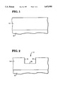
- FIGS. 1-3 are sequentially selected cross sectional views, at various stages of the fabrication of a semiconductor fusible link according to one form of the present invention.
- FIG. 4 is a top view of the fuse in FIG. 3. Selected hidden lines are shown in phantom.
- FIG. 5 is a a top view of a semiconductor fuse according to another form of the present invention. Selected hidden lines are shown in phantom.
- FIGS. 1-3 show selected views of a semiconductor device during the fabrication of a fusible link.
- an insulating layer 14 is formed on top of an underlying layer 12.
- layer 12 may be a silicon substrate.
- layer 12 is a metal layer such as metal 1.
- Insulating layer 14 may be provided in many different ways: For example, if layer 12 silicon, insulating layer 14 may be a thermally grown SiO 2 Alternatively, layer 14 can be deposited or applied as a spin-on-glass, such as a boron phosphorous silica glass. It is also possible to form insulating layer 14 by forming multiple insulating layers using one or more of the above processes.
- Layer 14 may be covered with photoresist which is then patterned and etched to form a trench 16 in insulating layer 14.
- Trench 16 has a number of flat surfaces. These surfaces intersect at relatively sharp edges. For a 90 degree angle, the maximum radius of the angle/formed by these surfaces is about 0.2 micrometers.
- trench 16 has a flat bottom surface 20 and essentially vertical sidewalls 18. Thus, the intersection of a sidewall 18 and bottom surface 20 forms a right angle.
- the invention is not limited to this specific configuration. Other configurations for trench 20 are possible--as long as the angle between the trench surfaces is relatively sharp and the angle of intersection is less than about 120 degrees.
- a fusible link 26 has been formed across insulating layer 14 and trench 16.
- Link 26 is formed by first depositing a layer of link material over the exposed surface of insulating layer 14 and trench 16.
- the link material is preferably a metal, and more specifically aluminum which is deposited by sputtering.
- the aluminum is deposited conformally with layer 14 and the surfaces defining trench 16.
- “conformally” means that the aluminum generally conforms to the upper surface of insulating layer 14, sidewalls 18 of trench 16 and the bottom surface 20 of trench 16.
- “conformally” does not mean that the outer surface of the aluminum is exactly geometrically similar to the surface on which it is deposited. The degree to which the material is not similar is influenced by the dimensions of trench 16, as will be described below.
- FIG. 4 shows a top view of the resulting link 26.
- Link 26 has a narrowed or necked down region 28 which has a minimum width, i.e., a smaller width than the rest of fusible link 26.
- Necked down region 28 is bounded by transition regions 30 and 32. Each region 30 and 32 marks the transition between the wider portion of fusible link 26 and necked down region 28. In the FIG. 4 embodiment, necked down region 28 overlies trench 16.
- fusible link 26 has a generally uniform thickness except in a break region 34.
- break region is a region where the fuse is most likely to break when subject to a programming or fuse blowing current.
- a shadowing effect (described more fully below) occurs, resulting in the thickness profile of link 26 as shown.
- This profile includes the two convex outer surfaces 40 and 42 of link 26.
- Convex surface 40 is formed along sidewall 18 and convex surface 42 is formed along bottom surface 20 of trench 16.
- Break region-34 is formed by the sharp intersection 50 of convex surfaces 40 and 42 which is at the intersection 52 of sidewall 18 and bottom surface 20 of trench 16. Intersection 50 is essentially closer to intersection 52 than any other point on the outer surface of link 26.
- FIG. 3 shows a characteristic shadowing profile of a deposited link material.
- trench 16 has a small length (L) and a somewhat larger depth (D).
- the ratio of depth to length is referred to as the aspect ratio.
- D/L the ratio of depth to length.
- the thickness "A" at break region 34 is significantly less than the thickness "C" of the rest of link 26. In fact, if D/L>1, A/C ⁇ 0.3.
- the minimum thickness of link 26 occurs in break region 34. Break region 34 also falls within necked down region 28 of link 26 where the width of link 26 is also a minimum. Thus, the cross sectional area of link 26 is a minimum at break region 34. It will be appreciated, that on the opposite side of trench 16 there is another break region 34a which has roughly the same minimum cross sectional area as break region 34.
- the "width" of a metal line is normal to both the direction of current flow and to the thickness of the metal line.
- the cross sectional area of a metal line such as link 26 is the area through which current can flow.
- the cross sectional area at a point along its length is the product of the width and thickness of the line at that point.
- fusible link 26 In operation, if fusible link 26 is to be "blown", a programming current in excess of the normal operating current is passed through link 26. Current passing therethrough, heats link 26. Since the minimum cross sectional area occurs in break region 34, the current density and hence the heating will be its greatest in break region 34. Thus, when subject to a programming current, break region 34 gets hotter than the rest of link 26. When the temperature is sufficiently high, link 26 melts. This design allows the temperature of in the break region to be high enough to provide a clean break during the melt which results in a reduced chance for the fuse to grow back.
- FIG. 5 is a top view of fuse 10 according to an alternative embodiment of the present invention.
- metal link 26a extends across trench 16 so that it covers sidewalls at ends 18a and 18b.
- FIG. 5 embodiment only a single sidewall 18a is covered by necked down region 28.
- link 26 has a break region 34 only at one end of trench 16.
- the advantage of the FIG. 5 embodiment is that it is a higher density configuration; thus, less area is required.
Abstract
Description
Claims (8)
Priority Applications (1)
| Application Number | Priority Date | Filing Date | Title |
|---|---|---|---|
| US07/935,306 US5672905A (en) | 1992-08-26 | 1992-08-26 | Semiconductor fuse and method |
Applications Claiming Priority (1)
| Application Number | Priority Date | Filing Date | Title |
|---|---|---|---|
| US07/935,306 US5672905A (en) | 1992-08-26 | 1992-08-26 | Semiconductor fuse and method |
Publications (1)
| Publication Number | Publication Date |
|---|---|
| US5672905A true US5672905A (en) | 1997-09-30 |
Family
ID=25466898
Family Applications (1)
| Application Number | Title | Priority Date | Filing Date |
|---|---|---|---|
| US07/935,306 Expired - Lifetime US5672905A (en) | 1992-08-26 | 1992-08-26 | Semiconductor fuse and method |
Country Status (1)
| Country | Link |
|---|---|
| US (1) | US5672905A (en) |
Cited By (10)
| Publication number | Priority date | Publication date | Assignee | Title |
|---|---|---|---|---|
| WO1998027595A1 (en) * | 1996-12-18 | 1998-06-25 | Intel Corporation | A silicide agglomeration fuse device with notches to enhance programmability |
| US5936296A (en) * | 1997-06-23 | 1999-08-10 | Samsung Electronics Co., Ltd. | Integrated circuits having metallic fuse links |
| US5969404A (en) * | 1995-09-29 | 1999-10-19 | Intel Corporation | Silicide agglomeration device |
| US6078092A (en) * | 1999-10-18 | 2000-06-20 | Harvatek Corporation | Resettable fuse integrated circuit package |
| US6190986B1 (en) | 1999-01-04 | 2001-02-20 | International Business Machines Corporation | Method of producing sulithographic fuses using a phase shift mask |
| US6323111B1 (en) | 1999-10-28 | 2001-11-27 | Agere Systems Guardian Corp | Preweakened on chip metal fuse using dielectric trenches for barrier layer isolation |
| US6323534B1 (en) | 1999-04-16 | 2001-11-27 | Micron Technology, Inc. | Fuse for use in a semiconductor device |
| US6388305B1 (en) | 1999-12-17 | 2002-05-14 | International Business Machines Corporation | Electrically programmable antifuses and methods for forming the same |
| US20130089976A1 (en) * | 2009-06-30 | 2013-04-11 | Hynix Semiconductor Inc. | Fuse structure for high integrated semiconductor device |
| CN109087904A (en) * | 2018-08-01 | 2018-12-25 | 深圳市南硕明泰科技有限公司 | Trim resistance and preparation method thereof |
Citations (20)
| Publication number | Priority date | Publication date | Assignee | Title |
|---|---|---|---|---|
| US4045310A (en) * | 1976-05-03 | 1977-08-30 | Teletype Corporation | Starting product for the production of a read-only memory and a method of producing it and the read-only memory |
| US4064493A (en) * | 1976-06-03 | 1977-12-20 | Motorola, Inc. | P-ROM Cell having a low current fusible programming link |
| GB2005078A (en) * | 1977-09-30 | 1979-04-11 | Philips Nv | Programmable read-only memory cell |
| US4198744A (en) * | 1978-08-16 | 1980-04-22 | Harris Corporation | Process for fabrication of fuse and interconnects |
| JPS5685846A (en) * | 1979-12-14 | 1981-07-13 | Fujitsu Ltd | Semiconductor integrated circuit device |
| US4312046A (en) * | 1979-10-04 | 1982-01-19 | Harris Corporation | Vertical fuse and method of fabrication |
| US4424578A (en) * | 1980-07-14 | 1984-01-03 | Tokyo Shibaura Denki Kabushiki Kaisha | Bipolar prom |
| US4441167A (en) * | 1981-12-03 | 1984-04-03 | Raytheon Company | Reprogrammable read only memory |
| SU986198A1 (en) * | 1980-12-25 | 1985-03-30 | Институт Радиотехники И Электроники Ан Ссср | Single-programmed memory |
| US4590589A (en) * | 1982-12-21 | 1986-05-20 | Zoran Corporation | Electrically programmable read only memory |
| US4647340A (en) * | 1986-03-31 | 1987-03-03 | Ncr Corporation | Programmable read only memory using a tungsten fuse |
| US4692787A (en) * | 1980-05-23 | 1987-09-08 | Texas Instruments Incorporated | Programmable read-only-memory element with polycrystalline silicon layer |
| EP0241046A2 (en) * | 1986-04-11 | 1987-10-14 | Nec Corporation | Semiconductor device having fuse-type memory element |
| US5017510A (en) * | 1987-06-01 | 1991-05-21 | Texas Instruments Incorporated | Method of making a scalable fuse link element |
| JPH03124047A (en) * | 1989-10-06 | 1991-05-27 | Nec Ic Microcomput Syst Ltd | Integrated circuit device |
| US5120679A (en) * | 1991-06-04 | 1992-06-09 | Vlsi Technology, Inc. | Anti-fuse structures and methods for making same |
| WO1993004499A1 (en) * | 1991-08-19 | 1993-03-04 | Crosspoint Solutions, Inc. | An improved antifuse and method of manufacture thereof |
| US5241212A (en) * | 1990-05-01 | 1993-08-31 | Mitsubishi Denki Kabushiki Kaisha | Semiconductor device having a redundant circuit portion and a manufacturing method of the same |
| US5244836A (en) * | 1991-12-30 | 1993-09-14 | North American Philips Corporation | Method of manufacturing fusible links in semiconductor devices |
| US5258643A (en) * | 1991-07-25 | 1993-11-02 | Massachusetts Institute Of Technology | Electrically programmable link structures and methods of making same |
-
1992
- 1992-08-26 US US07/935,306 patent/US5672905A/en not_active Expired - Lifetime
Patent Citations (20)
| Publication number | Priority date | Publication date | Assignee | Title |
|---|---|---|---|---|
| US4045310A (en) * | 1976-05-03 | 1977-08-30 | Teletype Corporation | Starting product for the production of a read-only memory and a method of producing it and the read-only memory |
| US4064493A (en) * | 1976-06-03 | 1977-12-20 | Motorola, Inc. | P-ROM Cell having a low current fusible programming link |
| GB2005078A (en) * | 1977-09-30 | 1979-04-11 | Philips Nv | Programmable read-only memory cell |
| US4198744A (en) * | 1978-08-16 | 1980-04-22 | Harris Corporation | Process for fabrication of fuse and interconnects |
| US4312046A (en) * | 1979-10-04 | 1982-01-19 | Harris Corporation | Vertical fuse and method of fabrication |
| JPS5685846A (en) * | 1979-12-14 | 1981-07-13 | Fujitsu Ltd | Semiconductor integrated circuit device |
| US4692787A (en) * | 1980-05-23 | 1987-09-08 | Texas Instruments Incorporated | Programmable read-only-memory element with polycrystalline silicon layer |
| US4424578A (en) * | 1980-07-14 | 1984-01-03 | Tokyo Shibaura Denki Kabushiki Kaisha | Bipolar prom |
| SU986198A1 (en) * | 1980-12-25 | 1985-03-30 | Институт Радиотехники И Электроники Ан Ссср | Single-programmed memory |
| US4441167A (en) * | 1981-12-03 | 1984-04-03 | Raytheon Company | Reprogrammable read only memory |
| US4590589A (en) * | 1982-12-21 | 1986-05-20 | Zoran Corporation | Electrically programmable read only memory |
| US4647340A (en) * | 1986-03-31 | 1987-03-03 | Ncr Corporation | Programmable read only memory using a tungsten fuse |
| EP0241046A2 (en) * | 1986-04-11 | 1987-10-14 | Nec Corporation | Semiconductor device having fuse-type memory element |
| US5017510A (en) * | 1987-06-01 | 1991-05-21 | Texas Instruments Incorporated | Method of making a scalable fuse link element |
| JPH03124047A (en) * | 1989-10-06 | 1991-05-27 | Nec Ic Microcomput Syst Ltd | Integrated circuit device |
| US5241212A (en) * | 1990-05-01 | 1993-08-31 | Mitsubishi Denki Kabushiki Kaisha | Semiconductor device having a redundant circuit portion and a manufacturing method of the same |
| US5120679A (en) * | 1991-06-04 | 1992-06-09 | Vlsi Technology, Inc. | Anti-fuse structures and methods for making same |
| US5258643A (en) * | 1991-07-25 | 1993-11-02 | Massachusetts Institute Of Technology | Electrically programmable link structures and methods of making same |
| WO1993004499A1 (en) * | 1991-08-19 | 1993-03-04 | Crosspoint Solutions, Inc. | An improved antifuse and method of manufacture thereof |
| US5244836A (en) * | 1991-12-30 | 1993-09-14 | North American Philips Corporation | Method of manufacturing fusible links in semiconductor devices |
Cited By (23)
| Publication number | Priority date | Publication date | Assignee | Title |
|---|---|---|---|---|
| US6258700B1 (en) | 1995-09-29 | 2001-07-10 | Intel Corporation | Silicide agglomeration fuse device |
| US5969404A (en) * | 1995-09-29 | 1999-10-19 | Intel Corporation | Silicide agglomeration device |
| US6337507B1 (en) * | 1995-09-29 | 2002-01-08 | Intel Corporation | Silicide agglomeration fuse device with notches to enhance programmability |
| GB2334820A (en) * | 1996-12-18 | 1999-09-01 | Intel Corp | A silicide agglomeration fuse device with notches to enhance programmability |
| WO1998027595A1 (en) * | 1996-12-18 | 1998-06-25 | Intel Corporation | A silicide agglomeration fuse device with notches to enhance programmability |
| US5936296A (en) * | 1997-06-23 | 1999-08-10 | Samsung Electronics Co., Ltd. | Integrated circuits having metallic fuse links |
| US6190986B1 (en) | 1999-01-04 | 2001-02-20 | International Business Machines Corporation | Method of producing sulithographic fuses using a phase shift mask |
| US6278171B2 (en) | 1999-01-04 | 2001-08-21 | International Business Machines Corporation | Sublithographic fuses using a phase shift mask |
| US20030211661A1 (en) * | 1999-04-16 | 2003-11-13 | Marr Kenneth W. | Fuse for use in a semiconductor device, and semiconductor devices including the fuse |
| US6979601B2 (en) | 1999-04-16 | 2005-12-27 | Micron Technology, Inc. | Methods for fabricating fuses for use in semiconductor devices and semiconductor devices including such fuses |
| US6323534B1 (en) | 1999-04-16 | 2001-11-27 | Micron Technology, Inc. | Fuse for use in a semiconductor device |
| US6879018B2 (en) | 1999-04-16 | 2005-04-12 | Micron Technology, Inc. | Fuse for use in a semiconductor device, and semiconductor devices including the fuse |
| US6410367B2 (en) | 1999-04-16 | 2002-06-25 | Micron Technology, Inc. | Fuse for use in a semiconductor device, and semiconductor devices including the fuse |
| US6495902B2 (en) | 1999-04-16 | 2002-12-17 | Micron Technology, Inc. | Fuse for use in a semiconductor device, and semiconductor devices including the fuse |
| US6551864B2 (en) | 1999-04-16 | 2003-04-22 | Micron Technology, Inc. | Fuse for use in a semiconductor device, and semiconductor devices including the fuse |
| US6078092A (en) * | 1999-10-18 | 2000-06-20 | Harvatek Corporation | Resettable fuse integrated circuit package |
| US6570238B2 (en) | 1999-10-28 | 2003-05-27 | Agere Systems Inc. | Preweakened on chip metal fuse using dielectric trenches for barrier layer isolation |
| US6323111B1 (en) | 1999-10-28 | 2001-11-27 | Agere Systems Guardian Corp | Preweakened on chip metal fuse using dielectric trenches for barrier layer isolation |
| US6812122B2 (en) | 1999-12-17 | 2004-11-02 | International Business Machines Corporation | Method for forming a voltage programming element |
| US6388305B1 (en) | 1999-12-17 | 2002-05-14 | International Business Machines Corporation | Electrically programmable antifuses and methods for forming the same |
| US20130089976A1 (en) * | 2009-06-30 | 2013-04-11 | Hynix Semiconductor Inc. | Fuse structure for high integrated semiconductor device |
| US9196527B2 (en) * | 2009-06-30 | 2015-11-24 | SK Hynix Inc. | Fuse structure for high integrated semiconductor device |
| CN109087904A (en) * | 2018-08-01 | 2018-12-25 | 深圳市南硕明泰科技有限公司 | Trim resistance and preparation method thereof |
Similar Documents
| Publication | Publication Date | Title |
|---|---|---|
| US5672905A (en) | Semiconductor fuse and method | |
| EP0083211B1 (en) | Semiconductor device with fuse | |
| US8184465B2 (en) | Programmable semiconductor device | |
| KR100374214B1 (en) | Vertical fuse and method of fabrication | |
| US6551864B2 (en) | Fuse for use in a semiconductor device, and semiconductor devices including the fuse | |
| US7382036B2 (en) | Doped single crystal silicon silicided eFuse | |
| US5753539A (en) | Method of making an integrated circuit with windowed fuse element and contact pad | |
| KR101058318B1 (en) | Self-aligned, planar phase change memory elements and devices, systems employing the same and methods of forming the same | |
| JP2003115575A (en) | One time programmable unit memory cell based on vertical fuse and diode and one time programmable memory comprising it | |
| US5015604A (en) | Fabrication method using oxidation to control size of fusible link | |
| KR100430667B1 (en) | Improved fuse link structures through the addition of dummy structures | |
| JPH0628290B2 (en) | Semiconductor device with circuit fuse | |
| US5963825A (en) | Method of fabrication of semiconductor fuse with polysilicon plate | |
| USRE46970E1 (en) | Diode-less array for one-time programmable memory | |
| EP0445317B1 (en) | Semiconductor device with a fusible link and method of making a fusible link on a semiconductor substrate | |
| US4414242A (en) | Process for fabricating a semiconductor device | |
| US5510642A (en) | Semiconductor device | |
| US4801351A (en) | Method of manufacturing monocrystalline thin-film | |
| EP0618620B1 (en) | Semiconductor fuse structures | |
| JPH0969570A (en) | Semiconductor device and its manufacture | |
| US20070190751A1 (en) | Semiconductor fuses and methods for fabricating and programming the same | |
| JPS5928374A (en) | Semiconductor integrated circuit device and manufacture thereof | |
| NL1010154C2 (en) | Ion implantation method for semiconductor manufacture e.g. DRAM - by determining surface layer thickness through which implantation can be carried out, providing it and implanting ions into substrate | |
| KR970006982Y1 (en) | One-time programmable rom structure with poly silicon fuse | |
| JPH03250620A (en) | Manufacture of semiconductor device |
Legal Events
| Date | Code | Title | Description |
|---|---|---|---|
| AS | Assignment |
Owner name: NCR CORPORATION, A CORP. OF MD, OHIO Free format text: ASSIGNMENT OF ASSIGNORS INTEREST.;ASSIGNORS:LEE, STEVEN S.;MILLER, GAYLE W.;REEL/FRAME:006245/0964 Effective date: 19920819 |
|
| AS | Assignment |
Owner name: HYUNDAI ELECTRONICS AMERICA Free format text: ASSIGNMENT OF ASSIGNORS INTEREST;ASSIGNOR:AT&T GLOBAL INFORMATION SOLUTIONS COMPANY (FORMERLY KNOWN AS NCR CORPORATION);REEL/FRAME:007408/0104 Effective date: 19950215 |
|
| AS | Assignment |
Owner name: SYMBIOS LOGIC INC., COLORADO Free format text: ASSIGNMENT OF ASSIGNORS INTEREST;ASSIGNOR:HYUNDAI ELECTRONICS AMERICA;REEL/FRAME:007629/0431 Effective date: 19950818 |
|
| STCF | Information on status: patent grant |
Free format text: PATENTED CASE |
|
| AS | Assignment |
Owner name: SYMBIOS, INC ., COLORADO Free format text: CHANGE OF NAME;ASSIGNOR:SYMBIOS LOGIC INC.;REEL/FRAME:009089/0936 Effective date: 19971210 |
|
| AS | Assignment |
Owner name: LEHMAN COMMERCIAL PAPER INC., AS ADMINISTRATIVE AG Free format text: SECURITY AGREEMENT;ASSIGNORS:HYUNDAI ELECTRONICS AMERICA, A CORP. OF CALIFORNIA;SYMBIOS, INC., A CORP. OF DELAWARE;REEL/FRAME:009396/0441 Effective date: 19980226 |
|
| AS | Assignment |
Owner name: HYUNDAI ELECTRONICS AMERICA, CALIFORNIA Free format text: TERMINATION AND LICENSE AGREEMENT;ASSIGNOR:SYMBIOS, INC.;REEL/FRAME:009596/0539 Effective date: 19980806 |
|
| FEPP | Fee payment procedure |
Free format text: PAYOR NUMBER ASSIGNED (ORIGINAL EVENT CODE: ASPN); ENTITY STATUS OF PATENT OWNER: LARGE ENTITY |
|
| FPAY | Fee payment |
Year of fee payment: 4 |
|
| AS | Assignment |
Owner name: HYNIX SEMICONDUCTOR AMERICA INC., CALIFORNIA Free format text: CHANGE OF NAME;ASSIGNOR:HYUNDAI ELECTRONICS AMERICA;REEL/FRAME:015246/0599 Effective date: 20010412 Owner name: HYNIX SEMICONDUCTOR INC., KOREA, REPUBLIC OF Free format text: ASSIGNMENT OF ASSIGNORS INTEREST;ASSIGNOR:HYNIX SEMICONDUCTOR AMERICA, INC.;REEL/FRAME:015279/0556 Effective date: 20040920 |
|
| AS | Assignment |
Owner name: MAGNACHIP SEMICONDUCTOR, LTD., KOREA, REPUBLIC OF Free format text: ASSIGNMENT OF ASSIGNORS INTEREST;ASSIGNOR:HYNIX SEMICONDUCTOR, INC.;REEL/FRAME:016216/0649 Effective date: 20041004 |
|
| FPAY | Fee payment |
Year of fee payment: 8 |
|
| AS | Assignment |
Owner name: U.S. BANK NATIONAL ASSOCIATION, AS COLLATERAL TRUS Free format text: SECURITY INTEREST;ASSIGNOR:MAGNACHIP SEMICONDUCTOR, LTD.;REEL/FRAME:016470/0530 Effective date: 20041223 |
|
| AS | Assignment |
Owner name: SYMBIOS, INC., COLORADO Free format text: RELEASE OF SECURITY INTEREST;ASSIGNOR:LEHMAN COMMERICAL PAPER INC.;REEL/FRAME:016602/0895 Effective date: 20050107 Owner name: HYUNDAI ELECTRONICS AMERICA, CALIFORNIA Free format text: RELEASE OF SECURITY INTEREST;ASSIGNOR:LEHMAN COMMERICAL PAPER INC.;REEL/FRAME:016602/0895 Effective date: 20050107 |
|
| AS | Assignment |
Owner name: TAIWAN SEMICONDUCTOR MANUFACTURING CO., LTD., TAIW Free format text: ASSIGNMENT OF ASSIGNORS INTEREST;ASSIGNORS:NCR CORPORATION;MAGNACHIP SEMICONDUCTOR, LTD.;REEL/FRAME:021398/0702;SIGNING DATES FROM 20071114 TO 20071115 |
|
| FPAY | Fee payment |
Year of fee payment: 12 |