US5684675A - Semiconductor device unit having holder - Google Patents
Semiconductor device unit having holder Download PDFInfo
- Publication number
- US5684675A US5684675A US08/252,522 US25252294A US5684675A US 5684675 A US5684675 A US 5684675A US 25252294 A US25252294 A US 25252294A US 5684675 A US5684675 A US 5684675A
- Authority
- US
- United States
- Prior art keywords
- holder
- semiconductor device
- semiconductor devices
- leads
- device unit
- Prior art date
- Legal status (The legal status is an assumption and is not a legal conclusion. Google has not performed a legal analysis and makes no representation as to the accuracy of the status listed.)
- Expired - Fee Related
Links
Images


Classifications
-
- H—ELECTRICITY
- H01—ELECTRIC ELEMENTS
- H01L—SEMICONDUCTOR DEVICES NOT COVERED BY CLASS H10
- H01L25/00—Assemblies consisting of a plurality of individual semiconductor or other solid state devices ; Multistep manufacturing processes thereof
- H01L25/50—Multistep manufacturing processes of assemblies consisting of devices, each device being of a type provided for in group H01L27/00 or H01L29/00
-
- H—ELECTRICITY
- H01—ELECTRIC ELEMENTS
- H01L—SEMICONDUCTOR DEVICES NOT COVERED BY CLASS H10
- H01L23/00—Details of semiconductor or other solid state devices
- H01L23/02—Containers; Seals
- H01L23/04—Containers; Seals characterised by the shape of the container or parts, e.g. caps, walls
-
- H—ELECTRICITY
- H01—ELECTRIC ELEMENTS
- H01L—SEMICONDUCTOR DEVICES NOT COVERED BY CLASS H10
- H01L23/00—Details of semiconductor or other solid state devices
- H01L23/32—Holders for supporting the complete device in operation, i.e. detachable fixtures
-
- H—ELECTRICITY
- H01—ELECTRIC ELEMENTS
- H01L—SEMICONDUCTOR DEVICES NOT COVERED BY CLASS H10
- H01L23/00—Details of semiconductor or other solid state devices
- H01L23/48—Arrangements for conducting electric current to or from the solid state body in operation, e.g. leads, terminal arrangements ; Selection of materials therefor
- H01L23/488—Arrangements for conducting electric current to or from the solid state body in operation, e.g. leads, terminal arrangements ; Selection of materials therefor consisting of soldered or bonded constructions
- H01L23/495—Lead-frames or other flat leads
- H01L23/49503—Lead-frames or other flat leads characterised by the die pad
- H01L23/4951—Chip-on-leads or leads-on-chip techniques, i.e. inner lead fingers being used as die pad
-
- H—ELECTRICITY
- H01—ELECTRIC ELEMENTS
- H01L—SEMICONDUCTOR DEVICES NOT COVERED BY CLASS H10
- H01L23/00—Details of semiconductor or other solid state devices
- H01L23/48—Arrangements for conducting electric current to or from the solid state body in operation, e.g. leads, terminal arrangements ; Selection of materials therefor
- H01L23/488—Arrangements for conducting electric current to or from the solid state body in operation, e.g. leads, terminal arrangements ; Selection of materials therefor consisting of soldered or bonded constructions
- H01L23/495—Lead-frames or other flat leads
- H01L23/49568—Lead-frames or other flat leads specifically adapted to facilitate heat dissipation
-
- H—ELECTRICITY
- H01—ELECTRIC ELEMENTS
- H01L—SEMICONDUCTOR DEVICES NOT COVERED BY CLASS H10
- H01L25/00—Assemblies consisting of a plurality of individual semiconductor or other solid state devices ; Multistep manufacturing processes thereof
- H01L25/03—Assemblies consisting of a plurality of individual semiconductor or other solid state devices ; Multistep manufacturing processes thereof all the devices being of a type provided for in the same subgroup of groups H01L27/00 - H01L33/00, or in a single subclass of H10K, H10N, e.g. assemblies of rectifier diodes
- H01L25/10—Assemblies consisting of a plurality of individual semiconductor or other solid state devices ; Multistep manufacturing processes thereof all the devices being of a type provided for in the same subgroup of groups H01L27/00 - H01L33/00, or in a single subclass of H10K, H10N, e.g. assemblies of rectifier diodes the devices having separate containers
- H01L25/105—Assemblies consisting of a plurality of individual semiconductor or other solid state devices ; Multistep manufacturing processes thereof all the devices being of a type provided for in the same subgroup of groups H01L27/00 - H01L33/00, or in a single subclass of H10K, H10N, e.g. assemblies of rectifier diodes the devices having separate containers the devices being of a type provided for in group H01L27/00
-
- H—ELECTRICITY
- H05—ELECTRIC TECHNIQUES NOT OTHERWISE PROVIDED FOR
- H05K—PRINTED CIRCUITS; CASINGS OR CONSTRUCTIONAL DETAILS OF ELECTRIC APPARATUS; MANUFACTURE OF ASSEMBLAGES OF ELECTRICAL COMPONENTS
- H05K3/00—Apparatus or processes for manufacturing printed circuits
- H05K3/30—Assembling printed circuits with electric components, e.g. with resistor
- H05K3/301—Assembling printed circuits with electric components, e.g. with resistor by means of a mounting structure
-
- H—ELECTRICITY
- H01—ELECTRIC ELEMENTS
- H01L—SEMICONDUCTOR DEVICES NOT COVERED BY CLASS H10
- H01L2225/00—Details relating to assemblies covered by the group H01L25/00 but not provided for in its subgroups
- H01L2225/03—All the devices being of a type provided for in the same subgroup of groups H01L27/00 - H01L33/648 and H10K99/00
- H01L2225/10—All the devices being of a type provided for in the same subgroup of groups H01L27/00 - H01L33/648 and H10K99/00 the devices having separate containers
- H01L2225/1005—All the devices being of a type provided for in the same subgroup of groups H01L27/00 - H01L33/648 and H10K99/00 the devices having separate containers the devices being of a type provided for in group H01L27/00
- H01L2225/1011—All the devices being of a type provided for in the same subgroup of groups H01L27/00 - H01L33/648 and H10K99/00 the devices having separate containers the devices being of a type provided for in group H01L27/00 the containers being in a stacked arrangement
- H01L2225/1017—All the devices being of a type provided for in the same subgroup of groups H01L27/00 - H01L33/648 and H10K99/00 the devices having separate containers the devices being of a type provided for in group H01L27/00 the containers being in a stacked arrangement the lowermost container comprising a device support
- H01L2225/1029—All the devices being of a type provided for in the same subgroup of groups H01L27/00 - H01L33/648 and H10K99/00 the devices having separate containers the devices being of a type provided for in group H01L27/00 the containers being in a stacked arrangement the lowermost container comprising a device support the support being a lead frame
-
- H—ELECTRICITY
- H01—ELECTRIC ELEMENTS
- H01L—SEMICONDUCTOR DEVICES NOT COVERED BY CLASS H10
- H01L2225/00—Details relating to assemblies covered by the group H01L25/00 but not provided for in its subgroups
- H01L2225/03—All the devices being of a type provided for in the same subgroup of groups H01L27/00 - H01L33/648 and H10K99/00
- H01L2225/10—All the devices being of a type provided for in the same subgroup of groups H01L27/00 - H01L33/648 and H10K99/00 the devices having separate containers
- H01L2225/1005—All the devices being of a type provided for in the same subgroup of groups H01L27/00 - H01L33/648 and H10K99/00 the devices having separate containers the devices being of a type provided for in group H01L27/00
- H01L2225/1011—All the devices being of a type provided for in the same subgroup of groups H01L27/00 - H01L33/648 and H10K99/00 the devices having separate containers the devices being of a type provided for in group H01L27/00 the containers being in a stacked arrangement
- H01L2225/1047—Details of electrical connections between containers
- H01L2225/107—Indirect electrical connections, e.g. via an interposer, a flexible substrate, using TAB
-
- H—ELECTRICITY
- H01—ELECTRIC ELEMENTS
- H01L—SEMICONDUCTOR DEVICES NOT COVERED BY CLASS H10
- H01L2225/00—Details relating to assemblies covered by the group H01L25/00 but not provided for in its subgroups
- H01L2225/03—All the devices being of a type provided for in the same subgroup of groups H01L27/00 - H01L33/648 and H10K99/00
- H01L2225/10—All the devices being of a type provided for in the same subgroup of groups H01L27/00 - H01L33/648 and H10K99/00 the devices having separate containers
- H01L2225/1005—All the devices being of a type provided for in the same subgroup of groups H01L27/00 - H01L33/648 and H10K99/00 the devices having separate containers the devices being of a type provided for in group H01L27/00
- H01L2225/1011—All the devices being of a type provided for in the same subgroup of groups H01L27/00 - H01L33/648 and H10K99/00 the devices having separate containers the devices being of a type provided for in group H01L27/00 the containers being in a stacked arrangement
- H01L2225/1094—Thermal management, e.g. cooling
-
- H—ELECTRICITY
- H01—ELECTRIC ELEMENTS
- H01L—SEMICONDUCTOR DEVICES NOT COVERED BY CLASS H10
- H01L2924/00—Indexing scheme for arrangements or methods for connecting or disconnecting semiconductor or solid-state bodies as covered by H01L24/00
- H01L2924/0001—Technical content checked by a classifier
- H01L2924/0002—Not covered by any one of groups H01L24/00, H01L24/00 and H01L2224/00
-
- Y—GENERAL TAGGING OF NEW TECHNOLOGICAL DEVELOPMENTS; GENERAL TAGGING OF CROSS-SECTIONAL TECHNOLOGIES SPANNING OVER SEVERAL SECTIONS OF THE IPC; TECHNICAL SUBJECTS COVERED BY FORMER USPC CROSS-REFERENCE ART COLLECTIONS [XRACs] AND DIGESTS
- Y10—TECHNICAL SUBJECTS COVERED BY FORMER USPC
- Y10S—TECHNICAL SUBJECTS COVERED BY FORMER USPC CROSS-REFERENCE ART COLLECTIONS [XRACs] AND DIGESTS
- Y10S269/00—Work holders
- Y10S269/903—Work holder for electrical circuit assemblages or wiring systems
Definitions
- the present invention generally relates to semiconductor device units and methods of mounting semiconductor devices, and more particularly to a semiconductor device unit having a holder, and to a method of mounting semiconductor devices using the holder.
- DRAMs dynamic random access memories
- small and thin packages such as the small outline package (SOP), the single in-line package (SIP) and the zigzag in-line package (ZIP) are known as package structures which enable high density packaging.
- SOP small outline package
- SIP single in-line package
- ZIP zigzag in-line package
- the SOP is a kind of surface package (surface mount).
- SOP type semiconductor device is arranged on solder bumps which are formed on a circuit substrate, and the solder is thereafter melted to fix the semiconductor device.
- a vertical type package such as the SIP and the ZIP has a structure such that leads are arranged in line along one side surface of the package. Accordingly, this vertical type package is mounted vertically on the circuit substrate.
- the packaging density is improved by this vertical mounting, and in addition, it is possible to improve the cooling efficiency of the package.
- Another and more specific object of the present invention is to provide a semiconductor device unit comprising a holder having a plurality of holding parts, and a plurality of semiconductor devices held by the holding parts of the holder, where each of the semiconductor devices have a generally parallelepiped shape with top and bottom surfaces and at least one side surface provided with leads which are exposed when the semiconductor device is held by the holding part of the holder.
- the semiconductor device unit of the present invention it is possible to make the semiconductor devices stand vertically on a circuit substrate because the semiconductor devices are held by the holder.
- the pitch with which the semiconductor devices may be arranged on the circuit substrate is improved, particularly when two or more semiconductor devices are held by one holding part of the holder. Therefore, the present invention can realize a high density packaging.
- the holder protects the relatively thin semiconductor devices the mechanical strength of which is not very large. Furthermore, the heat generated from the semiconductor device is transferred to the holder by thermal conduction and the heat resistance of the semiconductor device unit as a whole is improved compared to that of the semiconductor device itself.
- Still another object of the present invention is to provide a method of mounting a plurality of semiconductor devices having leads provided on at least one side surface thereof onto a circuit substrate, comprising the steps of (a) holding the semiconductor devices in holding parts of a holder so that the leads are exposed, and (b) mounting the semiconductor devices held by the holder onto the circuit substrate by connecting the exposed leads to the circuit substrate.
- the method of the present invention it is possible to make the semiconductor devices stand vertically on a circuit substrate because the semiconductor devices are held by the holder.
- the pitch with which the semiconductor devices may be arranged on the circuit substrate is improved, particularly when two or more semiconductor devices are held by one holding part of the holder. Therefore, the present invention can realize a high density packaging.
- the holder protects the relatively thin semiconductor devices the mechanical strength of which is not very large. Furthermore, the heat generated from the semiconductor device is transferred to the holder by thermal conduction and the heat resistance of the semiconductor device unit as a whole is improved compared to that of the semiconductor device itself.
- FIG. 1 is a perspective view showing a first embodiment of a semiconductor device unit according to the present invention
- FIG. 2 is a perspective view showing a semiconductor device shown in FIG. 1;
- FIG. 3 is a perspective view for explaining holding of the semiconductor devices in a holder shown in FIG. 1;
- FIGS. 4A through 4D are perspective views for explaining the soldering of leads of the semiconductor devices on a circuit substrate shown in FIG. 1;
- FIG. 5 is a perspective view showing a second embodiment of the semiconductor device unit according to the present invention.
- FIG. 6 is a perspective view showing a third embodiment of the semiconductor device unit according to the present invention.
- FIG. 7 is a perspective view showing a fourth embodiment of the semiconductor device unit according to the present invention.
- FIG. 8 is a perspective view showing a semiconductor device to which the present invention may be applied.
- FIG. 9 is a perspective view showing another semiconductor device to which the present invention may be applied.
- FIG. 10 is a perspective view showing a fifth embodiment of the semiconductor device unit according to the present invention.
- FIG. 11 is a perspective view showing a sixth embodiment of the semiconductor device unit according to the present invention.
- FIG. 12 is a perspective view showing a seventh embodiment of the semiconductor device unit according to the present invention.
- FIG. 13 is a perspective view showing an eighth embodiment of the semiconductor device unit according to the present invention.
- FIG. 14 is a perspective view showing a ninth embodiment of the semiconductor device unit according to the present invention.
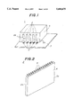
- FIG. 1 shows the first embodiment, and in FIG. 1, a semiconductor device unit 1 includes semiconductor devices 2 and a holder 3 which holds the semiconductor devices 2.
- the semiconductor device 2 may be a memory device such as a DRAM, and a plurality of semiconductor devices having the same construction are packaged on a single circuit substrate 7.
- Each semiconductor device 2 has the vertical package structure shown on an enlarged scale in FIG. 2.
- a plurality of leads 5 extend outwardly from one side surface of a package 4 which is made of a resin.
- a semiconductor element such as a memory device is encapsulated within the package 4. Because the package 4 is relatively thin, the mechanical strength of the semiconductor device 2 itself is poor and its heat resistance is large.
- the leads 5 are bent in an L-shape at the tip extension thereof.
- the semiconductor device 2 having the vertical package structure shown in FIG. 2 does not easily stand by itself on the circuit substrate 7. Even if it were possible to make the semiconductor device 2 stand by itself on the circuit substrate 7, the semiconductor device 2 would be too unstable to allow satisfactory soldering of the leads 5 onto the circuit substrate 7.
- the semiconductor devices 2 which by themselves cannot stably stand on the circuit substrate 7 are held by the holder 3 so that the semiconductor devices 2 stand stably on the circuit substrate 7 when soldering the leads 5 onto the circuit substrate 7.
- the holder 3 is molded from a resin and has a box shape as shown in FIG. 3.
- the holder 3 has five holding parts 6 for receiving the semiconductor devices 2.
- Each holding part 6 opens at the front and bottom surfaces of the holder 3.
- the holding parts 6 may be formed at the same time as molding the holder 3 by known means.
- each semiconductor device 2 is inserted into the corresponding holding part 6 of the holder 3.
- the semiconductor device unit 1 is assembled by this simple operation. Hence, the packaging process will not become complex and will not greatly increase the number of production steps by this process of assembling the semiconductor device unit 1.
- a mask 100 including a plurality of windows 101 is placed on the circuit substrate 7 so that each window 101 matches a corresponding region 105 where the solder is to be applied.
- a roll of solder 107 rolls in a direction of an arrow over the mask 100 to form the solder 107 on the regions 105 of the circuit substrate 7 via the windows 101.
- solder parts 107a are formed in the regions 105 of the circuit substrate 7.
- each semiconductor device 2 (only one shown for the sake of convenience) is placed on the circuit substrate 7 so that the leads 5 rest on the corresponding solder parts 107a. Then, a reflow process is carried out to connect the leads 5 onto the circuit substrate 7 by the melted solder parts 107a.
- FIG. 1 shows the semiconductor device unit 1 in the assembled state, and the semiconductor devices 2 are held within the holder 3.
- the leads extend downwardly from each of the semiconductor devices 2 within the holder 3. Accordingly, although each semiconductor device 2 by itself cannot stand stably on the circuit substrate 7, the semiconductor devices 2 within the holder 2 cooperate and stand stably on the circuit substrate 7. There is no need to provide holes in the circuit substrate 7 as in the case of the proposed structure described above, and it is possible to improve the packaging efficiency. In addition, because the semiconductor devices 2 are held by the holder 3, it is possible to reduce the pitch with which the semiconductor devices 2 are arranged on the circuit substrate 7 and realize a high packaging density.
- the package 4 is relatively thin and the semiconductor device 2 by itself does not have a satisfactory mechanical strength and has a large heat resistance.
- the package 4 of each semiconductor device 2 is in contiguous contact with walls of the holder 3 defining the corresponding holding part 6.
- the holder 3 also functions as a support member for improving the mechanical strength of each semiconductor device 2, and cracks will not easily be formed in the package 4 although the package 4 itself is relatively thin.
- the heat generated from each semiconductor device 2 is transferred to the holder 3 by thermal conduction. As a result, the heat resistance of the semiconductor device unit 1 as a whole decreases compared to that of the semiconductor device 2 itself, and the heat is efficiently radiated. Therefore, it is possible to reduce the undesirable effects of heat on each of the semiconductor devices 2.
- FIG. 5 shows a second embodiment of the semiconductor device unit according to the present invention.
- a semiconductor device unit 11 shown in FIG. 5 includes a holder 13 and a plurality of semiconductor devices 2 held in holding parts 16 of the holder 13.
- the holding part 16 opens only at the bottom surface of the holder 13.
- the holding part 16 of the holder 13 is a rectangular well which opens only at the bottom surface of the holder 13.
- the semiconductor device 2 is buried in the holder 13 when the semiconductor device 2 is held by the holding part 16, and all of the outer surfaces of the semiconductor device 2 excluding the surface provided with the leads 5 make contiguous contact with the walls defining the holding part 16. Therefore, the mechanical strength of the semiconductor device 2 is improved compared to that of the first embodiment, and it is also possible to improve the cooling efficiency of the semiconductor device 2.
- FIG. 6 shows a third embodiment of the semiconductor device unit according to the present invention.
- those parts which are the same as those corresponding parts in FIGS. 1 through 3 are designated by the same reference numerals, and a description thereof will be omitted.
- a semiconductor device unit 21 shown in FIG. 6 includes a cooling fin 24 which is provided around selected outer surfaces of the holder 3.
- the cooling fin 24 is made of a metal, and improves the cooling efficiency of the semiconductor device 2.
- FIG. 7 shows a fourth embodiment of the semiconductor device unit according to the present invention.
- those parts which are the same as those corresponding parts in FIGS. 1 through 3 are designated by the same reference numerals, and a description thereof will be omitted.
- a semiconductor device unit 31 shown in FIG. 7 includes cooling fins 34 which are provided on the top surface of the holder 3.
- the cooling fins 34 improve the cooling efficiency of the semiconductor device 2.
- the holder 3 may be made of a metal or a plastic, and the cooling fins 24 and 34 may be made of a metal or a plastic.
- An arbitrary combination of materials may be used for the holder 3 and the cooling fins 24 and 34, but if the same material is used for the two, the cooling fins 24 and 34 may be integrally formed on the holder 3.
- the semiconductor device 2 has the L-shaped leads 5.
- semiconductor devices shown in FIGS. 8 and 9 may also be used in fifth through eighth embodiments which will be described later.
- a semiconductor device 2 1 shown in FIG. 8 has leads 5 1 which are arranged in a zigzag manner, so that the density of the leads 5 1 may be improved.
- a semiconductor device 2 2 shown in FIG. 9 has loop shaped leads 5 2 .
- the shape of the leads 5 2 would make it almost impossible for the semiconductor device 2 2 to stand by itself on the circuit substrate 7, but the present invention would enable a plurality of such semiconductor devices 2 2 to stably stand on the circuit substrate 7 by the use of the holder.
- FIG. 10 shows a fifth embodiment of the semiconductor device unit according to the present invention.
- those parts which are the same as those corresponding parts in FIGS. 1 through 3 are designated by the same reference numerals, and a description thereof will be omitted.
- a cooling fin 44 is provided on the left part of each semiconductor device 2 which is held by the holder 3, and each cooling fin 44 projects from the holder 3. As a result, the cooling effect of the semiconductor device 2 is improved.
- FIG. 11 shows a sixth embodiment of the semiconductor device unit according to the present invention.
- those parts which are the same as those corresponding parts in FIGS. 1 through 3 are designated by the same reference numerals, and a description thereof will be omitted.
- a cooling part 54 including a plurality of cooling pins 54a is provided on the top surface of the holder 3.
- the holder 3 may be made of a metal or a plastic, and the cooling part 54 may be made of a metal or a plastic.
- An arbitrary combination of materials may be used for the holder 3 and the cooling part 54, but if the same material is used for the two, the cooling part 54 may be integrally formed on the holder 3.
- FIG. 12 shows a seventh embodiment of the semiconductor device unit according to the present invention.
- those parts which are the same as those corresponding parts in FIGS. 1 through 3 are designated by the same reference numerals, and a description thereof will be omitted.
- a holding part 66 of the holder 63 holds only the top part of the semiconductor device 2. Walls of the holder 63 defining the holding part 66 make contiguous contact with the top part of the semiconductor device 2, and thus, the holder 63 can make the semiconductor devices 2 stand stably on the circuit substrate 7 when soldering the leads 5 onto the circuit substrate 7.
- FIG. 13 shows an eighth embodiment of the semiconductor device unit according to the present invention.
- those parts which are the same as those corresponding parts in FIGS. 1 through 3 are designated by the same reference numerals, and a description thereof will be omitted.
- a holder 72 has holding parts 76 V for vertically holding semiconductor devices 2 3 , and holding parts 76 H for horizontally holding the semiconductor devices 2.
- Each semiconductor device 2 3 has the leads 5 provided on two adjacent side surfaces thereof.
- the leads 5 of the semiconductor device 2 3 are exposed at the front and bottom surfaces of the holder 73.
- the semiconductor device 2 is held by the holding part 76 H of the holder 73, the leads of the semiconductor device 2 are exposed at the front surface of the holder 73.
- both the leads 5 exposed at the front surface of the holder 73 and the leads 5 exposed at the bottom surface of the holder 73 can be soldered onto the circuit substrate 7.
- This embodiment is thus advantageous in that the semiconductor devices 2 3 having a large number of leads 5 can be packaged on the circuit substrates 7.
- different kinds of semiconductor devices can be positively supported by the holder 73 when making the packaging process.
- FIG. 14 shows a ninth embodiment of the semiconductor device unit according to the present invention.
- those parts which are the same as those corresponding parts in FIGS. 1 through 3 are designated by the same reference numerals, and a description thereof will be omitted.
- a holder 83 has two holding parts 86.
- Each holding part 86 holds three semiconductor devices 2 in contiguous contact therewith.
- the pitch with which the semiconductor devices 2 may be arranged on the circuit substrate 7 may further be improved.
- the number of semiconductor devices 2 held by each holding part 86 of the holder 83 is not limited to three, and an arbitrary number of semiconductor devices 2 greater than one may be held by each holding part 86.
- the shape of the holder is not limited to that of the described embodiments.
- the holder in the described embodiments has a generally parallelepiped shape in conformance with the generally parallelepiped shape of the semiconductor device, but it is of course possible to employ other shapes for the holder.
- the side surface of the semiconductor device exposed at the front of the holder does not necessarily have to coincide with the front surface of the holder.
- the end part of the semiconductor device may project slightly from the front surface of the holder.
Abstract
A semiconductor device unit includes a holder having a plurality of holding parts, and a plurality of semiconductor devices held by the holding parts of the holder. Each of the semiconductor devices has a generally parallelepiped shape with top and bottom surfaces and at least one side surface provided with leads which are exposed whereby the semiconductor device unit stands by itself on the leads.
Description
This application is a continuation of application Ser. No. 08/152,883, filed Nov. 16, 1993, and now abandoned which is a continuation of application Ser. No. 07/889,955, filed May 29, 1992, now abandoned.
The present invention generally relates to semiconductor device units and methods of mounting semiconductor devices, and more particularly to a semiconductor device unit having a holder, and to a method of mounting semiconductor devices using the holder.
Recently, as the size of computer systems has further been reduced, there are demands to package semiconductor devices with a high density.
On the other hand, in memory devices such as dynamic random access memories (DRAMs), a plurality of semiconductor devices having the same construction are packaged on a single circuit substrate. Accordingly, there are demands to realize a method of packaging a plurality of semiconductor devices having the same construction with a high efficiency.
In order to increase the packaging density, the package structure becomes an important factor. Conventionally, small and thin packages such as the small outline package (SOP), the single in-line package (SIP) and the zigzag in-line package (ZIP) are known as package structures which enable high density packaging.
The SOP is a kind of surface package (surface mount). In other words, SOP type semiconductor device is arranged on solder bumps which are formed on a circuit substrate, and the solder is thereafter melted to fix the semiconductor device.
On the other hand, a vertical type package such as the SIP and the ZIP has a structure such that leads are arranged in line along one side surface of the package. Accordingly, this vertical type package is mounted vertically on the circuit substrate. The packaging density is improved by this vertical mounting, and in addition, it is possible to improve the cooling efficiency of the package.
However, in the case of the SOP, there are problems in that a crack is easily formed in the package because it has a thin flat shape and the heat resistance of the package becomes large. In addition, because the package is surface mounted, there is also a problem in that the packaging area is large compared to that of the SIP, for example.
In the case of the SIP and ZIP, there are problems in that it is difficult to make the package stand because the leads extend outwardly from one side surface thereof and the packaging (or mounting) process is troublesome to perform.
For this reason, a structure has been proposed to help the vertical package stand on the circuit substrate. According to this proposed structure, projections are formed on the package, and holes corresponding to the projections are provided in the circuit substrate. The vertical package stands on the circuit substrate in a state where the projections fit into the corresponding holes of the circuit substrate. However, according to this proposed structure, there are problems in that the holes must be formed in the circuit substrate and the production efficiency becomes poor due to this additional step of forming the holes.
On the other hand, when the vertical package such as the SIP and the ZIP are made thin, there are problems in that a crack is easily formed in the package and the heat resistance of the package becomes large.
Accordingly, it is a general object of the present invention to provide a novel and useful semiconductor device unit and method of mounting semiconductor devices, in which the problems described above are eliminated.
Another and more specific object of the present invention is to provide a semiconductor device unit comprising a holder having a plurality of holding parts, and a plurality of semiconductor devices held by the holding parts of the holder, where each of the semiconductor devices have a generally parallelepiped shape with top and bottom surfaces and at least one side surface provided with leads which are exposed when the semiconductor device is held by the holding part of the holder. According to the semiconductor device unit of the present invention, it is possible to make the semiconductor devices stand vertically on a circuit substrate because the semiconductor devices are held by the holder. The pitch with which the semiconductor devices may be arranged on the circuit substrate is improved, particularly when two or more semiconductor devices are held by one holding part of the holder. Therefore, the present invention can realize a high density packaging. In addition, the holder protects the relatively thin semiconductor devices the mechanical strength of which is not very large. Furthermore, the heat generated from the semiconductor device is transferred to the holder by thermal conduction and the heat resistance of the semiconductor device unit as a whole is improved compared to that of the semiconductor device itself.
Still another object of the present invention is to provide a method of mounting a plurality of semiconductor devices having leads provided on at least one side surface thereof onto a circuit substrate, comprising the steps of (a) holding the semiconductor devices in holding parts of a holder so that the leads are exposed, and (b) mounting the semiconductor devices held by the holder onto the circuit substrate by connecting the exposed leads to the circuit substrate. According to the method of the present invention, it is possible to make the semiconductor devices stand vertically on a circuit substrate because the semiconductor devices are held by the holder. The pitch with which the semiconductor devices may be arranged on the circuit substrate is improved, particularly when two or more semiconductor devices are held by one holding part of the holder. Therefore, the present invention can realize a high density packaging. In addition, the holder protects the relatively thin semiconductor devices the mechanical strength of which is not very large. Furthermore, the heat generated from the semiconductor device is transferred to the holder by thermal conduction and the heat resistance of the semiconductor device unit as a whole is improved compared to that of the semiconductor device itself.
Other objects and further features of the present invention will be apparent from the following detailed description when read in conjunction with the accompanying drawings.
FIG. 1 is a perspective view showing a first embodiment of a semiconductor device unit according to the present invention;
FIG. 2 is a perspective view showing a semiconductor device shown in FIG. 1;
FIG. 3 is a perspective view for explaining holding of the semiconductor devices in a holder shown in FIG. 1;
FIGS. 4A through 4D are perspective views for explaining the soldering of leads of the semiconductor devices on a circuit substrate shown in FIG. 1;
FIG. 5 is a perspective view showing a second embodiment of the semiconductor device unit according to the present invention;
FIG. 6 is a perspective view showing a third embodiment of the semiconductor device unit according to the present invention;
FIG. 7 is a perspective view showing a fourth embodiment of the semiconductor device unit according to the present invention;
FIG. 8 is a perspective view showing a semiconductor device to which the present invention may be applied;
FIG. 9 is a perspective view showing another semiconductor device to which the present invention may be applied;
FIG. 10 is a perspective view showing a fifth embodiment of the semiconductor device unit according to the present invention;
FIG. 11 is a perspective view showing a sixth embodiment of the semiconductor device unit according to the present invention;
FIG. 12 is a perspective view showing a seventh embodiment of the semiconductor device unit according to the present invention;
FIG. 13 is a perspective view showing an eighth embodiment of the semiconductor device unit according to the present invention; and
FIG. 14 is a perspective view showing a ninth embodiment of the semiconductor device unit according to the present invention.
A description will be given of a first embodiment of a semiconductor device unit according to the present invention. FIG. 1 shows the first embodiment, and in FIG. 1, a semiconductor device unit 1 includes semiconductor devices 2 and a holder 3 which holds the semiconductor devices 2.
For example, the semiconductor device 2 may be a memory device such as a DRAM, and a plurality of semiconductor devices having the same construction are packaged on a single circuit substrate 7. Each semiconductor device 2 has the vertical package structure shown on an enlarged scale in FIG. 2. In the semiconductor device 2 shown in FIG. 2, a plurality of leads 5 extend outwardly from one side surface of a package 4 which is made of a resin. A semiconductor element (not shown) such as a memory device is encapsulated within the package 4. Because the package 4 is relatively thin, the mechanical strength of the semiconductor device 2 itself is poor and its heat resistance is large. On the other hand, as shown in FIG. 2, the leads 5 are bent in an L-shape at the tip extension thereof.
The semiconductor device 2 having the vertical package structure shown in FIG. 2 does not easily stand by itself on the circuit substrate 7. Even if it were possible to make the semiconductor device 2 stand by itself on the circuit substrate 7, the semiconductor device 2 would be too unstable to allow satisfactory soldering of the leads 5 onto the circuit substrate 7.
According to the present invention, the semiconductor devices 2 which by themselves cannot stably stand on the circuit substrate 7 are held by the holder 3 so that the semiconductor devices 2 stand stably on the circuit substrate 7 when soldering the leads 5 onto the circuit substrate 7.
For example, the holder 3 is molded from a resin and has a box shape as shown in FIG. 3. In this embodiment, the holder 3 has five holding parts 6 for receiving the semiconductor devices 2. Each holding part 6 opens at the front and bottom surfaces of the holder 3. The holding parts 6 may be formed at the same time as molding the holder 3 by known means.
When assembling the semiconductor device unit 1, each semiconductor device 2 is inserted into the corresponding holding part 6 of the holder 3. The semiconductor device unit 1 is assembled by this simple operation. Hence, the packaging process will not become complex and will not greatly increase the number of production steps by this process of assembling the semiconductor device unit 1.
Next, a description will be given of the method of soldering the leads 5 of the semiconductor devices 2 onto the circuit substrate 7, by referring to FIGS. 4A through 4D.
First, in FIG. 4A, a mask 100 including a plurality of windows 101 is placed on the circuit substrate 7 so that each window 101 matches a corresponding region 105 where the solder is to be applied.
Second, in FIG. 4B, a roll of solder 107 rolls in a direction of an arrow over the mask 100 to form the solder 107 on the regions 105 of the circuit substrate 7 via the windows 101.
Third, in FIG. 4C, the mask 100 is removed, and as a result, solder parts 107a are formed in the regions 105 of the circuit substrate 7.
Fourth, in FIG. 4D, each semiconductor device 2 (only one shown for the sake of convenience) is placed on the circuit substrate 7 so that the leads 5 rest on the corresponding solder parts 107a. Then, a reflow process is carried out to connect the leads 5 onto the circuit substrate 7 by the melted solder parts 107a.
FIG. 1 shows the semiconductor device unit 1 in the assembled state, and the semiconductor devices 2 are held within the holder 3. The leads extend downwardly from each of the semiconductor devices 2 within the holder 3. Accordingly, although each semiconductor device 2 by itself cannot stand stably on the circuit substrate 7, the semiconductor devices 2 within the holder 2 cooperate and stand stably on the circuit substrate 7. There is no need to provide holes in the circuit substrate 7 as in the case of the proposed structure described above, and it is possible to improve the packaging efficiency. In addition, because the semiconductor devices 2 are held by the holder 3, it is possible to reduce the pitch with which the semiconductor devices 2 are arranged on the circuit substrate 7 and realize a high packaging density.
The package 4 is relatively thin and the semiconductor device 2 by itself does not have a satisfactory mechanical strength and has a large heat resistance. However, when the semiconductor devices 2 are held by the holder 3, the package 4 of each semiconductor device 2 is in contiguous contact with walls of the holder 3 defining the corresponding holding part 6. For this reason, the holder 3 also functions as a support member for improving the mechanical strength of each semiconductor device 2, and cracks will not easily be formed in the package 4 although the package 4 itself is relatively thin. Furthermore, the heat generated from each semiconductor device 2 is transferred to the holder 3 by thermal conduction. As a result, the heat resistance of the semiconductor device unit 1 as a whole decreases compared to that of the semiconductor device 2 itself, and the heat is efficiently radiated. Therefore, it is possible to reduce the undesirable effects of heat on each of the semiconductor devices 2.
FIG. 5 shows a second embodiment of the semiconductor device unit according to the present invention. A semiconductor device unit 11 shown in FIG. 5 includes a holder 13 and a plurality of semiconductor devices 2 held in holding parts 16 of the holder 13. In this embodiment, the holding part 16 opens only at the bottom surface of the holder 13. Hence, compared to the first embodiment shown in FIG. 1 in which a side surface 2a of each semiconductor device 2 held by the holder 3 is exposed to the outside, the mechanical strength and the heat resistance of the semiconductor device 2 is improved in this second embodiment.
In other words, the holding part 16 of the holder 13 is a rectangular well which opens only at the bottom surface of the holder 13. For this reason, the semiconductor device 2 is buried in the holder 13 when the semiconductor device 2 is held by the holding part 16, and all of the outer surfaces of the semiconductor device 2 excluding the surface provided with the leads 5 make contiguous contact with the walls defining the holding part 16. Therefore, the mechanical strength of the semiconductor device 2 is improved compared to that of the first embodiment, and it is also possible to improve the cooling efficiency of the semiconductor device 2.
FIG. 6 shows a third embodiment of the semiconductor device unit according to the present invention. In FIG. 6, those parts which are the same as those corresponding parts in FIGS. 1 through 3 are designated by the same reference numerals, and a description thereof will be omitted.
A semiconductor device unit 21 shown in FIG. 6 includes a cooling fin 24 which is provided around selected outer surfaces of the holder 3. For example, the cooling fin 24 is made of a metal, and improves the cooling efficiency of the semiconductor device 2.
FIG. 7 shows a fourth embodiment of the semiconductor device unit according to the present invention. In FIG. 7, those parts which are the same as those corresponding parts in FIGS. 1 through 3 are designated by the same reference numerals, and a description thereof will be omitted.
A semiconductor device unit 31 shown in FIG. 7 includes cooling fins 34 which are provided on the top surface of the holder 3. The cooling fins 34 improve the cooling efficiency of the semiconductor device 2.
In FIGS. 6 and 7, the holder 3 may be made of a metal or a plastic, and the cooling fins 24 and 34 may be made of a metal or a plastic. An arbitrary combination of materials may be used for the holder 3 and the cooling fins 24 and 34, but if the same material is used for the two, the cooling fins 24 and 34 may be integrally formed on the holder 3.
In the embodiments described above, the semiconductor device 2 has the L-shaped leads 5. However, it is possible to use other types of semiconductor devices such as the semiconductor devices shown in FIGS. 8 and 9. The semiconductor devices shown in FIGS. 8 and 9 may also be used in fifth through eighth embodiments which will be described later.
A semiconductor device 21 shown in FIG. 8 has leads 51 which are arranged in a zigzag manner, so that the density of the leads 51 may be improved.
A semiconductor device 22 shown in FIG. 9 has loop shaped leads 52. The shape of the leads 52 would make it almost impossible for the semiconductor device 22 to stand by itself on the circuit substrate 7, but the present invention would enable a plurality of such semiconductor devices 22 to stably stand on the circuit substrate 7 by the use of the holder.
FIG. 10 shows a fifth embodiment of the semiconductor device unit according to the present invention. In FIG. 10, those parts which are the same as those corresponding parts in FIGS. 1 through 3 are designated by the same reference numerals, and a description thereof will be omitted.
According to a semiconductor device unit 41 shown in FIG. 10, a cooling fin 44 is provided on the left part of each semiconductor device 2 which is held by the holder 3, and each cooling fin 44 projects from the holder 3. As a result, the cooling effect of the semiconductor device 2 is improved.
FIG. 11 shows a sixth embodiment of the semiconductor device unit according to the present invention. In FIG. 11, those parts which are the same as those corresponding parts in FIGS. 1 through 3 are designated by the same reference numerals, and a description thereof will be omitted.
According to a semiconductor device unit 51 shown in FIG. 11, a cooling part 54 including a plurality of cooling pins 54a is provided on the top surface of the holder 3. The holder 3 may be made of a metal or a plastic, and the cooling part 54 may be made of a metal or a plastic. An arbitrary combination of materials may be used for the holder 3 and the cooling part 54, but if the same material is used for the two, the cooling part 54 may be integrally formed on the holder 3.
FIG. 12 shows a seventh embodiment of the semiconductor device unit according to the present invention. In FIG. 12, those parts which are the same as those corresponding parts in FIGS. 1 through 3 are designated by the same reference numerals, and a description thereof will be omitted.
According to a semiconductor device unit 61 shown in FIG. 12, only the top part of each semiconductor device 2 is fit into a holder 63. In other words, a holding part 66 of the holder 63 holds only the top part of the semiconductor device 2. Walls of the holder 63 defining the holding part 66 make contiguous contact with the top part of the semiconductor device 2, and thus, the holder 63 can make the semiconductor devices 2 stand stably on the circuit substrate 7 when soldering the leads 5 onto the circuit substrate 7.
FIG. 13 shows an eighth embodiment of the semiconductor device unit according to the present invention. In FIG. 13, those parts which are the same as those corresponding parts in FIGS. 1 through 3 are designated by the same reference numerals, and a description thereof will be omitted.
According to a semiconductor device unit 71 shown in FIG. 13, a holder 72 has holding parts 76V for vertically holding semiconductor devices 23, and holding parts 76H for horizontally holding the semiconductor devices 2. Each semiconductor device 23 has the leads 5 provided on two adjacent side surfaces thereof. When the semiconductor device 23 is held by the holding part 76V of the holder 73, the leads 5 of the semiconductor device 23 are exposed at the front and bottom surfaces of the holder 73. On the other hand, when the semiconductor device 2 is held by the holding part 76H of the holder 73, the leads of the semiconductor device 2 are exposed at the front surface of the holder 73. Therefore, according to this embodiment, both the leads 5 exposed at the front surface of the holder 73 and the leads 5 exposed at the bottom surface of the holder 73 can be soldered onto the circuit substrate 7. This embodiment is thus advantageous in that the semiconductor devices 23 having a large number of leads 5 can be packaged on the circuit substrates 7. In addition, different kinds of semiconductor devices can be positively supported by the holder 73 when making the packaging process.
FIG. 14 shows a ninth embodiment of the semiconductor device unit according to the present invention. In FIG. 14, those parts which are the same as those corresponding parts in FIGS. 1 through 3 are designated by the same reference numerals, and a description thereof will be omitted.
According to a semiconductor device unit 81 shown in FIG. 14, a holder 83 has two holding parts 86. Each holding part 86 holds three semiconductor devices 2 in contiguous contact therewith. As a result, the pitch with which the semiconductor devices 2 may be arranged on the circuit substrate 7 may further be improved. Of course, the number of semiconductor devices 2 held by each holding part 86 of the holder 83 is not limited to three, and an arbitrary number of semiconductor devices 2 greater than one may be held by each holding part 86.
In each of the embodiments described above, it is desirable that no air exists between the surfaces of the semiconductor device and the walls of the holder holding at least a part of the semiconductor device. In order to ensure contiguous contact between the contacting surfaces of the semiconductor device and the walls defining the holding part of the holder, it is possible to coat a lubricant such as grease on the surface of the semiconductor device and/or the walls defining the holding part of the holder.
In addition, the shape of the holder is not limited to that of the described embodiments. In other words, the holder in the described embodiments has a generally parallelepiped shape in conformance with the generally parallelepiped shape of the semiconductor device, but it is of course possible to employ other shapes for the holder.
Moreover, in each of the embodiments excluding the second embodiment, the side surface of the semiconductor device exposed at the front of the holder does not necessarily have to coincide with the front surface of the holder. In other words, the end part of the semiconductor device may project slightly from the front surface of the holder.
Further, the present invention is not limited to these embodiments, but various variations and modifications may be made without departing from the scope of the present invention.
Claims (23)
1. A semiconductor device unit supporting semiconductor devices on a horizontally extending substrate comprising:
a holder formed of a resin, having a plurality of internal holding parts extending in a first direction and a bottom, each of the holding parts having a slot structure opening toward the bottom of the holder; and
a plurality of semiconductor devices in the form of resin encapsulated packages extending in the first direction, with leads, the semiconductor devices being releasably retained by the holding parts of said holder for release from the holder through openings in the slot structures, the leads of the semiconductor devices being exposed outside of the holder such that the holder and the semiconductor devices retained therein are releasably supported upon the horizontally extending substrate by only the exposed leads of the semiconductor devices,
each of said semiconductor devices having a generally parallelepiped shape with parallel front and back side surfaces and a bottom surface provided with the leads which are exposed outside of the holder, the front and back side surfaces extending in the first direction and the bottom surface extending in a second direction which is generally perpendicular to the first direction, said leads extending laterally from the bottom surface, for each of the plurality of semiconductor devices, the entire bottom surface is substantially smaller than the entire front side surface and substantially smaller than the entire back side surface.
2. The semiconductor device unit as claimed in claim 1, wherein the slot structures each have inner walls, each said semiconductor device being held between the inner walls of the slot structure.
3. The semiconductor device unit as claimed in claim 1, wherein the holding parts of said holder hold said semiconductor devices in a vertical arrangement and parallel to each other.
4. The semiconductor device unit as claimed in claim 1, wherein at least the bottom surface of each semiconductor device is exposed through the opening in the slot structure.
5. The semiconductor device unit as claimed in claim 1, wherein the holding parts of said holder have a well structure such that only the bottom surface of each semiconductor device is exposed.
6. The semiconductor device unit as claimed in claim 1, wherein only an end part of each semiconductor device excluding the end provided with the leads is held by said holder.
7. The semiconductor device unit as claimed in claim 1, wherein the bottom surface and a lateral side surface of each semiconductor device are exposed, the lateral side surface being perpendicular to and connecting the front and back side surfaces.
8. The semiconductor device unit as claimed in claim 7, wherein an end part of the semiconductor device including the bottom surface of the semiconductor device projects from said holder.
9. The semiconductor device unit as claimed in claim 1, which further comprises a cooling part provided on said holder for radiating heat generated from each semiconductor device.
10. The semiconductor device unit as claimed in claim 9, wherein said cooling part covers at least one predetermined outer surface of said holder.
11. The semiconductor device unit as claimed in claim 9, wherein said holder is made of a material selected from a group consisting of metals and plastics, and said cooling part is made of a material selected from a group consisting of metals and plastics.
12. The semiconductor device unit as claimed in claim 11, wherein said holder and said cooling part are integrally formed from the same material.
13. The semiconductor device unit as claimed in claim 1, wherein each holding part of said holder holds a plurality of semiconductor devices.
14. The semiconductor device unit as claimed in claim 1, wherein the holding parts of said holder include first holding parts vertically holding some of the semiconductor devices and second holder parts horizontally holding some of the semiconductor devices.
15. The semiconductor device unit as claimed in claim 1, wherein walls of said holder defining the holding part make contiguous contact with at least the front and back side surfaces of the semiconductor device which is held thereby.
16. The semiconductor device unit as claimed in claim 15, wherein a lubricant is coated on at least one of the walls of said holder defining the holding part and at least the front and back side surfaces of the semiconductor device which is held thereby.
17. The semiconductor device unit as claimed in claim 1, wherein the leads of the semiconductor device have a shape selected from a group consisting of an L-shape and a loop shape.
18. The semiconductor device unit as claimed in claim 1, wherein the leads of the semiconductor device are arranged in a zigzag pattern on the bottom surface thereof.
19. The semiconductor device unit as claimed in claim 1, wherein each of said semiconductor devices has a configuration such that the semiconductor device cannot stably stand vertically by itself on its exposed leads.
20. The semiconductor device unit as claimed in claim 1, wherein each holding part of said holder holds one semiconductor device.
21. A semiconductor device unit supporting semiconductor devices on a horizontally extending substrate comprising:
a holder formed of a resin having a plurality of internal holding parts extending in a first direction; and
a plurality of semiconductor devices in the form of resin encapsulated packages extending in the first direction, with leads, the semiconductor devices being releasably retained by the holding parts of said holder with the leads exposed outside of the holder such that the holder and the semiconductor devices retained therein are releasably supported upon the horizontally extending substrate by only the exposed leads of the semiconductor devices,
each of said semiconductor devices having a generally parallelepiped shape with parallel front and back side surfaces and a bottom surface provided with the leads which are exposed outside of the holder, the front and back side surfaces extending in the first direction and the bottom surface extending in a second direction which is generally perpendicular to the first direction, said leads extending laterally from the bottom surface,
wherein the holding parts of said holder have a slot structure such that a lateral side surface and the bottom surface of each semiconductor device are exposed, the lateral side surface being perpendicular to and connecting the front and back side surfaces,
wherein each semiconductor device has a cooling fin which extends outwardly from the lateral side surface of the semiconductor device, and the cooling fin is exposed via the holding part which has the slot structure.
22. A semiconductor device unit supporting semiconductor devices on a horizontally extending substrate comprising:
a holder formed of a resink having a plurality of internal holding parts extending in a first direction and a bottom, each of the holding parts having a slot structure opening toward the bottom of the holder;
a plurality of semiconductor devices in the form of resin encapsulated packages extending in the first direction, with leads, the semiconductor devices being releasably retained by the holding parts of said holder for release from the holder through openings in the slot structures, the leads of the semiconductor devices being exposed outside of the holder such that the holder and the semiconductor devices retained therein are releasably supported upon the horizontally extending substrate by only the exposed leads of the semiconductor devices,
each of said semiconductor devices having a generally parallelepiped shape with parallel front and back side surfaces and a bottom surface provided with the leads which are exposed outside of the holder, the front and back side surfaces extending in the first direction and the bottom surface extending in a second direction which is generally perpendicular to the first direction, said leads extending laterally from the bottom surface, for each of the plurality of semiconductor devices, the entire bottom surface is substantially smaller than the entire front side surface and substantially smaller than the entire back side surface
a cooling part provided on said holder for radiating heat generated from each semiconductor device, wherein said cooling part comprises a plurality of pins which project from at least one predetermined outer surface of said holder.
23. A semiconductor device unit supporting semiconductor devices on a horizontally extending substrate comprising:
a holder formed of a resin having a plurality of internal holding parts extending in a first direction; and
a plurality of semiconductor devices in the form of resin encapsulated packages extending in the first direction, with leads, the semiconductor devices being releasably retained by the holding parts of said holder with the leads exposed outside of the holder such that the holder and the semiconductor devices retained therein are releasably supported upon the horizontally extending substrate by only the exposed leads of the semiconductor devices,
each of said semiconductor devices having a generally parallelepiped shape with parallel front and back side surfaces and a bottom surface provided with the leads which are exposed outside of the holder, the front and back side surfaces extending in the first direction and the bottom surface extending in a second direction which is generally perpendicular to the first direction, said leads extending laterally from the bottom surface,
wherein the holding parts of said holder include first holding parts vertically holding some of the semiconductor devices and second holding parts horizontally holding some of the semiconductor devices,
wherein the semiconductor devices held by the first holding part of said holder have leads provided on the bottom surface and a lateral side surface thereof, the lateral side surface being perpendicular to and connecting the front and back side surfaces.
Priority Applications (2)
| Application Number | Priority Date | Filing Date | Title |
|---|---|---|---|
| US08/252,522 US5684675A (en) | 1991-05-31 | 1994-06-01 | Semiconductor device unit having holder |
| US08/749,734 US5786985A (en) | 1991-05-31 | 1996-11-15 | Semiconductor device and semiconductor device unit |
Applications Claiming Priority (5)
| Application Number | Priority Date | Filing Date | Title |
|---|---|---|---|
| JP3-129776 | 1991-05-31 | ||
| JP3129776A JPH04354363A (en) | 1991-05-31 | 1991-05-31 | Semiconductor device unit |
| US88995592A | 1992-05-29 | 1992-05-29 | |
| US15288393A | 1993-11-16 | 1993-11-16 | |
| US08/252,522 US5684675A (en) | 1991-05-31 | 1994-06-01 | Semiconductor device unit having holder |
Related Parent Applications (1)
| Application Number | Title | Priority Date | Filing Date |
|---|---|---|---|
| US15288393A Continuation | 1991-05-31 | 1993-11-16 |
Related Child Applications (1)
| Application Number | Title | Priority Date | Filing Date |
|---|---|---|---|
| US46080395A Continuation-In-Part | 1991-05-31 | 1995-06-02 |
Publications (1)
| Publication Number | Publication Date |
|---|---|
| US5684675A true US5684675A (en) | 1997-11-04 |
Family
ID=15017936
Family Applications (1)
| Application Number | Title | Priority Date | Filing Date |
|---|---|---|---|
| US08/252,522 Expired - Fee Related US5684675A (en) | 1991-05-31 | 1994-06-01 | Semiconductor device unit having holder |
Country Status (5)
| Country | Link |
|---|---|
| US (1) | US5684675A (en) |
| EP (1) | EP0516096B1 (en) |
| JP (1) | JPH04354363A (en) |
| KR (1) | KR970000216B1 (en) |
| DE (1) | DE69212902T2 (en) |
Cited By (15)
| Publication number | Priority date | Publication date | Assignee | Title |
|---|---|---|---|---|
| US5978229A (en) * | 1996-12-07 | 1999-11-02 | Samsung Electronics Co., Ltd. | Circuit board |
| US6201695B1 (en) * | 1998-10-26 | 2001-03-13 | Micron Technology, Inc. | Heat sink for chip stacking applications |
| US6492720B1 (en) * | 2001-06-06 | 2002-12-10 | Mitsubishi Denki Kabushiki Kaisha | Flat-type semiconductor stack |
| US6496375B2 (en) * | 2001-04-30 | 2002-12-17 | Hewlett-Packard Company | Cooling arrangement for high density packaging of electronic components |
| US20050018401A1 (en) * | 2003-05-05 | 2005-01-27 | Christian Stocken | Device for cooling memory modules |
| US20050135067A1 (en) * | 2003-12-23 | 2005-06-23 | Sang-Wook Park | Semiconductor module with vertically mounted semiconductor chip packages |
| US20060221573A1 (en) * | 2005-04-04 | 2006-10-05 | Ming Li | Heat sink for multiple semiconductor modules |
| US20070290311A1 (en) * | 2006-05-24 | 2007-12-20 | Hauenstein Henning M | Bond wireless power module wiht double-sided single device cooling and immersion bath cooling |
| US20090016040A1 (en) * | 2007-07-10 | 2009-01-15 | Rohm Co., Ltd. | IC device and method of manufacturing the same |
| US20090321905A1 (en) * | 2008-06-27 | 2009-12-31 | Integrated Device Technology, Inc. | Multi-Package Ball Grid Array |
| US20100148334A1 (en) * | 1997-11-25 | 2010-06-17 | Micron Technology, Inc. | Intergrated circuit package support system |
| US20110304992A1 (en) * | 2010-06-15 | 2011-12-15 | Hon Hai Precision Industry Co., Ltd. | Heat dissipation device |
| US20110310567A1 (en) * | 2010-06-18 | 2011-12-22 | Hon Hai Precision Industry Co., Ltd. | Heat sink and electronic device using the same |
| US20120020004A1 (en) * | 2009-10-30 | 2012-01-26 | Hewlett-Packard Development Company, L.P. | Frame having frame blades that participate in cooling memory modules |
| US20190132995A1 (en) * | 2017-10-27 | 2019-05-02 | Micron Technology, Inc. | Assemblies including heat dispersing elements and related systems and methods |
Families Citing this family (5)
| Publication number | Priority date | Publication date | Assignee | Title |
|---|---|---|---|---|
| FR2688630B1 (en) * | 1992-03-13 | 2001-08-10 | Thomson Csf | METHOD AND DEVICE FOR THREE-DIMENSIONAL INTERCONNECTION OF ELECTRONIC COMPONENT PACKAGES. |
| JP3253765B2 (en) * | 1993-06-25 | 2002-02-04 | 富士通株式会社 | Semiconductor device |
| US5457071A (en) * | 1993-09-03 | 1995-10-10 | International Business Machine Corp. | Stackable vertical thin package/plastic molded lead-on-chip memory cube |
| DE19757612C1 (en) * | 1997-12-23 | 1999-07-08 | Siemens Ag | Hybrid circuit with a heat dissipation system |
| DE19846456A1 (en) * | 1998-10-08 | 2000-01-27 | Siemens Ag | Electronic component with semiconductor component and lead frame |
Citations (19)
| Publication number | Priority date | Publication date | Assignee | Title |
|---|---|---|---|---|
| US3579046A (en) * | 1969-05-02 | 1971-05-18 | Jordan Controls Inc | Electrical housing assembly having a plurality of chambers with adjacent circuit board elements |
| US3790859A (en) * | 1970-02-19 | 1974-02-05 | Texas Instruments Inc | Electronic package header system having omni-directional heat dissipation characteristic |
| US4220384A (en) * | 1978-10-20 | 1980-09-02 | Amp Incorporated | Loose piece terminal mounting assembly |
| US4227238A (en) * | 1977-09-28 | 1980-10-07 | Nippon Gakki Seizo Kabushiki Kaisha | Mounting and electrical connection means for operation unit for electric devices |
| US4420795A (en) * | 1981-08-17 | 1983-12-13 | Scholz Donald T | Electronic component mounting |
| US4498123A (en) * | 1983-03-25 | 1985-02-05 | Tellabs, Inc. | Universal circuit module mounting structure |
| US4553190A (en) * | 1982-08-26 | 1985-11-12 | Minnesota Mining And Manufacturing Co. | Transparent container for electrostatic sensitive electronic components |
| US4663695A (en) * | 1984-10-23 | 1987-05-05 | Honda Giken Kogyo Kabushiki Kaisha | Holding device for mounting an electronic component on a printed circuit board |
| US4667270A (en) * | 1984-10-31 | 1987-05-19 | Kitagawa Industries Co., Ltd. | Light emitting diode holder |
| US4720771A (en) * | 1985-07-05 | 1988-01-19 | Chrysler Motors Corporation | Heat sink assembly for a circuit board mounted integrated circuit |
| US4727456A (en) * | 1986-05-06 | 1988-02-23 | Northern Telecom Limited | Leadless electronic component carrier |
| US4814944A (en) * | 1985-08-14 | 1989-03-21 | Omron Tateisi Electronics Co. | Mounting structure for surface mounted type component with projection extending down from lower surface thereof and method of mounting a surface mounted type component on a printed circuit board |
| US4868712A (en) * | 1987-02-04 | 1989-09-19 | Woodman John K | Three dimensional integrated circuit package |
| US4894706A (en) * | 1985-02-14 | 1990-01-16 | Nippon Telegraph And Telephone Corporation | Three-dimensional packaging of semiconductor device chips |
| EP0354708A2 (en) * | 1988-08-08 | 1990-02-14 | Texas Instruments Incorporated | General three dimensional packaging |
| US4962442A (en) * | 1990-03-30 | 1990-10-09 | Thermalloy Incorporated | Free-standing stanchion for supporting and protecting electronic device packages on circuit boards |
| US4965699A (en) * | 1989-04-18 | 1990-10-23 | Magnavox Government And Industrial Electronics Company | Circuit card assembly cold plate |
| US5050039A (en) * | 1990-06-26 | 1991-09-17 | Digital Equipment Corporation | Multiple circuit chip mounting and cooling arrangement |
| US5057969A (en) * | 1990-09-07 | 1991-10-15 | International Business Machines Corporation | Thin film electronic device |
-
1991
- 1991-05-31 JP JP3129776A patent/JPH04354363A/en active Pending
-
1992
- 1992-05-27 DE DE69212902T patent/DE69212902T2/en not_active Expired - Fee Related
- 1992-05-27 EP EP92108972A patent/EP0516096B1/en not_active Expired - Lifetime
- 1992-06-01 KR KR1019920009499A patent/KR970000216B1/en not_active IP Right Cessation
-
1994
- 1994-06-01 US US08/252,522 patent/US5684675A/en not_active Expired - Fee Related
Patent Citations (19)
| Publication number | Priority date | Publication date | Assignee | Title |
|---|---|---|---|---|
| US3579046A (en) * | 1969-05-02 | 1971-05-18 | Jordan Controls Inc | Electrical housing assembly having a plurality of chambers with adjacent circuit board elements |
| US3790859A (en) * | 1970-02-19 | 1974-02-05 | Texas Instruments Inc | Electronic package header system having omni-directional heat dissipation characteristic |
| US4227238A (en) * | 1977-09-28 | 1980-10-07 | Nippon Gakki Seizo Kabushiki Kaisha | Mounting and electrical connection means for operation unit for electric devices |
| US4220384A (en) * | 1978-10-20 | 1980-09-02 | Amp Incorporated | Loose piece terminal mounting assembly |
| US4420795A (en) * | 1981-08-17 | 1983-12-13 | Scholz Donald T | Electronic component mounting |
| US4553190A (en) * | 1982-08-26 | 1985-11-12 | Minnesota Mining And Manufacturing Co. | Transparent container for electrostatic sensitive electronic components |
| US4498123A (en) * | 1983-03-25 | 1985-02-05 | Tellabs, Inc. | Universal circuit module mounting structure |
| US4663695A (en) * | 1984-10-23 | 1987-05-05 | Honda Giken Kogyo Kabushiki Kaisha | Holding device for mounting an electronic component on a printed circuit board |
| US4667270A (en) * | 1984-10-31 | 1987-05-19 | Kitagawa Industries Co., Ltd. | Light emitting diode holder |
| US4894706A (en) * | 1985-02-14 | 1990-01-16 | Nippon Telegraph And Telephone Corporation | Three-dimensional packaging of semiconductor device chips |
| US4720771A (en) * | 1985-07-05 | 1988-01-19 | Chrysler Motors Corporation | Heat sink assembly for a circuit board mounted integrated circuit |
| US4814944A (en) * | 1985-08-14 | 1989-03-21 | Omron Tateisi Electronics Co. | Mounting structure for surface mounted type component with projection extending down from lower surface thereof and method of mounting a surface mounted type component on a printed circuit board |
| US4727456A (en) * | 1986-05-06 | 1988-02-23 | Northern Telecom Limited | Leadless electronic component carrier |
| US4868712A (en) * | 1987-02-04 | 1989-09-19 | Woodman John K | Three dimensional integrated circuit package |
| EP0354708A2 (en) * | 1988-08-08 | 1990-02-14 | Texas Instruments Incorporated | General three dimensional packaging |
| US4965699A (en) * | 1989-04-18 | 1990-10-23 | Magnavox Government And Industrial Electronics Company | Circuit card assembly cold plate |
| US4962442A (en) * | 1990-03-30 | 1990-10-09 | Thermalloy Incorporated | Free-standing stanchion for supporting and protecting electronic device packages on circuit boards |
| US5050039A (en) * | 1990-06-26 | 1991-09-17 | Digital Equipment Corporation | Multiple circuit chip mounting and cooling arrangement |
| US5057969A (en) * | 1990-09-07 | 1991-10-15 | International Business Machines Corporation | Thin film electronic device |
Cited By (30)
| Publication number | Priority date | Publication date | Assignee | Title |
|---|---|---|---|---|
| US5978229A (en) * | 1996-12-07 | 1999-11-02 | Samsung Electronics Co., Ltd. | Circuit board |
| US7894192B2 (en) * | 1997-11-25 | 2011-02-22 | Round Rock Research, Llc | Integrated circuit package support system |
| US20100148334A1 (en) * | 1997-11-25 | 2010-06-17 | Micron Technology, Inc. | Intergrated circuit package support system |
| US8035974B1 (en) * | 1997-11-25 | 2011-10-11 | Round Rock Research, Llc | Integrated circuit package support system |
| US6201695B1 (en) * | 1998-10-26 | 2001-03-13 | Micron Technology, Inc. | Heat sink for chip stacking applications |
| US6449161B2 (en) * | 1998-10-26 | 2002-09-10 | Micron Technology, Inc. | Heat sink for chip stacking applications |
| US6707673B2 (en) | 1998-10-26 | 2004-03-16 | Micron Technology, Inc. | Heat sink for chip stacking applications |
| US6496375B2 (en) * | 2001-04-30 | 2002-12-17 | Hewlett-Packard Company | Cooling arrangement for high density packaging of electronic components |
| US6492720B1 (en) * | 2001-06-06 | 2002-12-10 | Mitsubishi Denki Kabushiki Kaisha | Flat-type semiconductor stack |
| US7023701B2 (en) * | 2003-05-05 | 2006-04-04 | Infineon Technologies, Ag | Device for cooling memory modules |
| US20050018401A1 (en) * | 2003-05-05 | 2005-01-27 | Christian Stocken | Device for cooling memory modules |
| US7050303B2 (en) * | 2003-12-23 | 2006-05-23 | Samsung Electronics Co., Ltd. | Semiconductor module with vertically mounted semiconductor chip packages |
| US20050135067A1 (en) * | 2003-12-23 | 2005-06-23 | Sang-Wook Park | Semiconductor module with vertically mounted semiconductor chip packages |
| US20060221573A1 (en) * | 2005-04-04 | 2006-10-05 | Ming Li | Heat sink for multiple semiconductor modules |
| WO2006107365A2 (en) * | 2005-04-04 | 2006-10-12 | Rambus Inc. | Heat sink for multiple semiconductor modules |
| WO2006107365A3 (en) * | 2005-04-04 | 2006-12-28 | Rambus Inc | Heat sink for multiple semiconductor modules |
| US20070290311A1 (en) * | 2006-05-24 | 2007-12-20 | Hauenstein Henning M | Bond wireless power module wiht double-sided single device cooling and immersion bath cooling |
| US8680666B2 (en) * | 2006-05-24 | 2014-03-25 | International Rectifier Corporation | Bond wireless power module with double-sided single device cooling and immersion bath cooling |
| US20090016040A1 (en) * | 2007-07-10 | 2009-01-15 | Rohm Co., Ltd. | IC device and method of manufacturing the same |
| US8139377B2 (en) * | 2007-07-10 | 2012-03-20 | Rohm Co., Ltd. | IC device and method of manufacturing the same |
| US7968989B2 (en) * | 2008-06-27 | 2011-06-28 | Integrated Device Technology, Inc | Multi-package slot array |
| US20090321905A1 (en) * | 2008-06-27 | 2009-12-31 | Integrated Device Technology, Inc. | Multi-Package Ball Grid Array |
| US20120020004A1 (en) * | 2009-10-30 | 2012-01-26 | Hewlett-Packard Development Company, L.P. | Frame having frame blades that participate in cooling memory modules |
| US8767403B2 (en) * | 2009-10-30 | 2014-07-01 | Hewlett-Packard Development Company, L.P. | Frame having frame blades that participate in cooling memory modules |
| US20110304992A1 (en) * | 2010-06-15 | 2011-12-15 | Hon Hai Precision Industry Co., Ltd. | Heat dissipation device |
| US20110310567A1 (en) * | 2010-06-18 | 2011-12-22 | Hon Hai Precision Industry Co., Ltd. | Heat sink and electronic device using the same |
| US8238105B2 (en) * | 2010-06-18 | 2012-08-07 | Hon Hai Precision Industry Co., Ltd. | Heat sink and electronic device using the same |
| US20190132995A1 (en) * | 2017-10-27 | 2019-05-02 | Micron Technology, Inc. | Assemblies including heat dispersing elements and related systems and methods |
| US10952352B2 (en) * | 2017-10-27 | 2021-03-16 | Micron Technology, Inc. | Assemblies including heat dispersing elements and related systems and methods |
| US11617284B2 (en) | 2017-10-27 | 2023-03-28 | Micron Technology, Inc. | Assemblies including heat dispersing elements and related systems and methods |
Also Published As
| Publication number | Publication date |
|---|---|
| DE69212902D1 (en) | 1996-09-26 |
| JPH04354363A (en) | 1992-12-08 |
| KR920022470A (en) | 1992-12-19 |
| KR970000216B1 (en) | 1997-01-06 |
| EP0516096A3 (en) | 1993-08-04 |
| EP0516096A2 (en) | 1992-12-02 |
| EP0516096B1 (en) | 1996-08-21 |
| DE69212902T2 (en) | 1997-04-03 |
Similar Documents
| Publication | Publication Date | Title |
|---|---|---|
| US5684675A (en) | Semiconductor device unit having holder | |
| US5444304A (en) | Semiconductor device having a radiating part | |
| US5260601A (en) | Edge-mounted, surface-mount package for semiconductor integrated circuit devices | |
| JPS59217345A (en) | Heat sink assembly | |
| JPH0221645A (en) | Surface mount package mounted by terminals for semiconductor integrated circuit device | |
| US20020051342A1 (en) | Radiator for electronic parts, electronic device, electric circuit device, and computer | |
| JP2878564B2 (en) | Semiconductor package | |
| US5786985A (en) | Semiconductor device and semiconductor device unit | |
| US5728601A (en) | Process for manufacturing a single in-line package for surface mounting | |
| US6967843B2 (en) | System and method for dissipating heat from an electronic board | |
| KR950012925B1 (en) | Lead frame | |
| JPH06177501A (en) | Memory module | |
| JPH0126111Y2 (en) | ||
| JPH09124092A (en) | Electronic component carrier | |
| KR970007848B1 (en) | Stack package and the manufacture method | |
| KR100216988B1 (en) | Power module | |
| US6549420B2 (en) | Method and apparatus for increasing memory capacity | |
| US4972043A (en) | Multi-lead hermetic power package with high packing density | |
| KR0126660Y1 (en) | Vertical mounted type package | |
| JP3761959B2 (en) | Mounting method of semiconductor device | |
| KR100257248B1 (en) | Power moudle | |
| JPH067252U (en) | heatsink | |
| JPH03205859A (en) | Semiconductor device | |
| JPH0577949U (en) | LSI package | |
| CN116417422A (en) | Semiconductor module |
Legal Events
| Date | Code | Title | Description |
|---|---|---|---|
| FEPP | Fee payment procedure |
Free format text: PAYOR NUMBER ASSIGNED (ORIGINAL EVENT CODE: ASPN); ENTITY STATUS OF PATENT OWNER: LARGE ENTITY |
|
| CC | Certificate of correction | ||
| FPAY | Fee payment |
Year of fee payment: 4 |
|
| REMI | Maintenance fee reminder mailed | ||
| LAPS | Lapse for failure to pay maintenance fees | ||
| STCH | Information on status: patent discontinuation |
Free format text: PATENT EXPIRED DUE TO NONPAYMENT OF MAINTENANCE FEES UNDER 37 CFR 1.362 |
|
| FP | Lapsed due to failure to pay maintenance fee |
Effective date: 20051104 |