US5700732A - Semiconductor wafer, wafer alignment patterns and method of forming wafer alignment patterns - Google Patents
Semiconductor wafer, wafer alignment patterns and method of forming wafer alignment patterns Download PDFInfo
- Publication number
- US5700732A US5700732A US08/691,855 US69185596A US5700732A US 5700732 A US5700732 A US 5700732A US 69185596 A US69185596 A US 69185596A US 5700732 A US5700732 A US 5700732A
- Authority
- US
- United States
- Prior art keywords
- wafer
- elevation
- alignment
- alignment pattern
- integrated circuitry
- Prior art date
- Legal status (The legal status is an assumption and is not a legal conclusion. Google has not performed a legal analysis and makes no representation as to the accuracy of the status listed.)
- Expired - Lifetime
Links
Images


Classifications
-
- H—ELECTRICITY
- H01—ELECTRIC ELEMENTS
- H01L—SEMICONDUCTOR DEVICES NOT COVERED BY CLASS H10
- H01L21/00—Processes or apparatus adapted for the manufacture or treatment of semiconductor or solid state devices or of parts thereof
- H01L21/67—Apparatus specially adapted for handling semiconductor or electric solid state devices during manufacture or treatment thereof; Apparatus specially adapted for handling wafers during manufacture or treatment of semiconductor or electric solid state devices or components ; Apparatus not specifically provided for elsewhere
- H01L21/67005—Apparatus not specifically provided for elsewhere
- H01L21/67242—Apparatus for monitoring, sorting or marking
- H01L21/67282—Marking devices
-
- G—PHYSICS
- G03—PHOTOGRAPHY; CINEMATOGRAPHY; ANALOGOUS TECHNIQUES USING WAVES OTHER THAN OPTICAL WAVES; ELECTROGRAPHY; HOLOGRAPHY
- G03F—PHOTOMECHANICAL PRODUCTION OF TEXTURED OR PATTERNED SURFACES, e.g. FOR PRINTING, FOR PROCESSING OF SEMICONDUCTOR DEVICES; MATERIALS THEREFOR; ORIGINALS THEREFOR; APPARATUS SPECIALLY ADAPTED THEREFOR
- G03F7/00—Photomechanical, e.g. photolithographic, production of textured or patterned surfaces, e.g. printing surfaces; Materials therefor, e.g. comprising photoresists; Apparatus specially adapted therefor
- G03F7/70—Microphotolithographic exposure; Apparatus therefor
-
- G—PHYSICS
- G03—PHOTOGRAPHY; CINEMATOGRAPHY; ANALOGOUS TECHNIQUES USING WAVES OTHER THAN OPTICAL WAVES; ELECTROGRAPHY; HOLOGRAPHY
- G03F—PHOTOMECHANICAL PRODUCTION OF TEXTURED OR PATTERNED SURFACES, e.g. FOR PRINTING, FOR PROCESSING OF SEMICONDUCTOR DEVICES; MATERIALS THEREFOR; ORIGINALS THEREFOR; APPARATUS SPECIALLY ADAPTED THEREFOR
- G03F9/00—Registration or positioning of originals, masks, frames, photographic sheets or textured or patterned surfaces, e.g. automatically
- G03F9/70—Registration or positioning of originals, masks, frames, photographic sheets or textured or patterned surfaces, e.g. automatically for microlithography
-
- H—ELECTRICITY
- H01—ELECTRIC ELEMENTS
- H01L—SEMICONDUCTOR DEVICES NOT COVERED BY CLASS H10
- H01L23/00—Details of semiconductor or other solid state devices
- H01L23/544—Marks applied to semiconductor devices or parts, e.g. registration marks, alignment structures, wafer maps
-
- H—ELECTRICITY
- H01—ELECTRIC ELEMENTS
- H01L—SEMICONDUCTOR DEVICES NOT COVERED BY CLASS H10
- H01L2223/00—Details relating to semiconductor or other solid state devices covered by the group H01L23/00
- H01L2223/544—Marks applied to semiconductor devices or parts
- H01L2223/5442—Marks applied to semiconductor devices or parts comprising non digital, non alphanumeric information, e.g. symbols
-
- H—ELECTRICITY
- H01—ELECTRIC ELEMENTS
- H01L—SEMICONDUCTOR DEVICES NOT COVERED BY CLASS H10
- H01L2223/00—Details relating to semiconductor or other solid state devices covered by the group H01L23/00
- H01L2223/544—Marks applied to semiconductor devices or parts
- H01L2223/54453—Marks applied to semiconductor devices or parts for use prior to dicing
-
- H—ELECTRICITY
- H01—ELECTRIC ELEMENTS
- H01L—SEMICONDUCTOR DEVICES NOT COVERED BY CLASS H10
- H01L2924/00—Indexing scheme for arrangements or methods for connecting or disconnecting semiconductor or solid-state bodies as covered by H01L24/00
- H01L2924/0001—Technical content checked by a classifier
- H01L2924/0002—Not covered by any one of groups H01L24/00, H01L24/00 and H01L2224/00
-
- Y—GENERAL TAGGING OF NEW TECHNOLOGICAL DEVELOPMENTS; GENERAL TAGGING OF CROSS-SECTIONAL TECHNOLOGIES SPANNING OVER SEVERAL SECTIONS OF THE IPC; TECHNICAL SUBJECTS COVERED BY FORMER USPC CROSS-REFERENCE ART COLLECTIONS [XRACs] AND DIGESTS
- Y10—TECHNICAL SUBJECTS COVERED BY FORMER USPC
- Y10S—TECHNICAL SUBJECTS COVERED BY FORMER USPC CROSS-REFERENCE ART COLLECTIONS [XRACs] AND DIGESTS
- Y10S148/00—Metal treatment
- Y10S148/102—Mask alignment
-
- Y—GENERAL TAGGING OF NEW TECHNOLOGICAL DEVELOPMENTS; GENERAL TAGGING OF CROSS-SECTIONAL TECHNOLOGIES SPANNING OVER SEVERAL SECTIONS OF THE IPC; TECHNICAL SUBJECTS COVERED BY FORMER USPC CROSS-REFERENCE ART COLLECTIONS [XRACs] AND DIGESTS
- Y10—TECHNICAL SUBJECTS COVERED BY FORMER USPC
- Y10S—TECHNICAL SUBJECTS COVERED BY FORMER USPC CROSS-REFERENCE ART COLLECTIONS [XRACs] AND DIGESTS
- Y10S438/00—Semiconductor device manufacturing: process
- Y10S438/975—Substrate or mask aligning feature
Definitions
- This invention relates generally to semiconductor wafer and photomask alignment, and to fabrication of semiconductor wafers having alignment patterns which facilitate the same.
- Photopatterning of semiconductive wafers requires precise positioning of a reticle or mask relative to the semiconductive wafer being processed. To achieve such precise positioning, the exact orientation or location of the wafer must be known such that the mask can be precisely placed. This is typically accomplished by moving the wafer beneath fixed optics which determine the wafer's precise location relative to a table on which the wafer rests and moves relative to the optics. The optics are directed toward the wafer to determine location of predetermined patterns provided in the wafer at least two discrete locations, such that wafer orientation is determined. With such known, the photomask and wafer can be precisely positioned in a desired relative orientation for processing.
- the wafer alignment patterns typically include discrete areas on the semiconductor substrate which are initially patterned to form multiple series of precisely configured parallel lines. In subsequent processing of the wafer, sometimes these wafer alignment patterns are masked such that they are not subjected to the specific processing, while other times they are left unmasked and are accordingly processed. For example, in some instances it is desirable to provide a planarized layer of a highly reflective or opaque material. Such a layer, because it is planarized, would not repeat the underlying pattern and substantially all incident light would be reflected away or absorbed. In such instance, the underlying alignment pattern would be lost. Accordingly in such instances, the wafer alignment pattern area would not be masked such that etching of such materials would not occur over the alignment patterns.
- the wafer alignment areas are typically masked during processing. Not masking of the wafer alignment pattern area throughout processing is typically not desired, as such would adversely effect overall global planarity of the wafer and eventually result in the wafer alignment patterns being received in deep holes or caverns. This would adversely effect the utility of the patterns and lead to other wafer processing problems. For example, whether an alignment step is masked or not masked during a photoexposure depends on several factors. These include, 1) the ability to see the alignment step at the next photo step; 2) the impact on the rest of the wafer, such as cracking and planarity; and 3) consistency in being able to get good alignment at all subsequent photosteps.
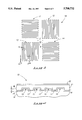
- FIGS. 1 and 2 illustrate a wafer alignment pattern indicated generally with reference numeral 10 patterned relative to a bulk monocrystalline silicon wafer 16. At least two of such patterns would be discretely located relative to the outer silicon wafer surface. Preferably, four of such discretely spaced patterns 10 are utilized.
- Wafer alignment pattern 10 is comprised of four discrete, or sub-discrete, alignment patterns 11, 12, 13 and 14. Wafer alignment pattern 10 is square, with each of sub-alignment patterns 11, 12, 13 and 14 also being square and located in one of the four quadrants of pattern 10. A central plus (+) 9 is centrally provided.
- Each pattern 11, 12, 13 and 14 comprises a plurality of patterned elevation steps/valleys/lines 15 initially provided in the outer surface of silicon substrate 16. Accordingly, lands or valley 17 (FIG. 2) are provided between elevation steps 15.
- the wafer alignment patterns utilize substantially a same, common elevation step change "A" between lands 17 and 15 throughout all wafer alignment patterns on the wafer, with an example being 1000 Angstroms. Further, all of the elevation steps are provided at a substantially common average elevation relative to the wafer. Such is indicated in FIG. 2 with numeral 18 as the elevation within wafer 16 between lands 17 and outer portion of elevation steps 15.
- FIG. 2 illustrates example subsequent layers deposited over wafer alignment pattern 10.
- Such include, for example, a conformal film 20, a planarized oxide layer 21, and an overlying planarized polysilicon layer 22. Both are suitably light transmissive to enable underlying topography to be perceived by laser light.
- the polysilicon of layer 22 has a substantially different refractive index from that of the oxide of layer 21. Depending upon the relative thicknesses of layers 21 and 22, this can create significant problems in achieving adequate contrast to determine underlying wafer pattern structure from steps 15 and lands 17. This results primarily from an undesired large quantity of light being reflected off the interface between planarized layers 21 and 22, as well as off the top of layer 22.
- Inherent thicknesses of such layers can also be a significant factor in achieving adequate contrast. For example in some instances, there are thicknesses of polysilicon layer 22 where poor contrast is obtained for a given elevation step height between lands 17 and step 15 for any thickness of planar oxide layer 21. Selecting a better polysilicon thickness greatly improves the situation, but there still exists oxide thicknesses where very poor contrast is obtained.
- FIG. 3 Such illustrates lines of constant reflectivity data as a function of thickness of a planarized polysilicon layer overlying a planarized oxide layer.
- Such data is relative to an underlying wafer alignment pattern having a 900 Angstrom elevation step change between lands 17 and peaks 15 and utilizing a 633 nanometer He--Ne laser imaging system. Areas where low or unacceptable contrast is obtained for determining wafer pattern location is depicted in the hatch-shaded areas of the graph. On the other hand, high or acceptable contrast is generally obtained in those illustrated areas where the illustrated lines of constant reflectivity form self-enclosed rings or ovals.
- areas 24 and 25 run substantially continuously across or over the illustrated graph, and constitute planarized oxide and planarized silicon combinations where unacceptably low contrast would be obtained.
- Other areas, such as 26, 27 and 28, are discretely independently enclosed and evidence areas where good contrast is obtained for determining the underlying wafer alignment pattern.
- planarized polysilicon thickness of, for example, 700 Angstroms and 1425 Angstroms result in poor contrast areas on the graph independent of oxide thickness. Accordingly in this example, the wafer processor would fundamentally avoid using planarized polysilicon layers of these thicknesses. The processor would rather attempt to operate in some other area of the depicted graph where adequate contrast is more likely. For example, for a polysilicon thickness of 1100 Angstroms, good example contrast is obtained for oxide thicknesses of between about 8625 Angstroms to about 9525 Angstroms. Yet, poor contrast would be obtained for such a polysilicon layer for oxide thicknesses of about 8500 Angstroms or about 8600 Angstroms.
- outer planarized polysilicon layer 22 is rather easy to control, whereas some underlying planarized layers such as oxide layer 21 are comparatively difficult to control.
- the processor can thereby avoid thicknesses of the outer layer which are inherently bad for any oxide thickness, but is left hoping that the less controllable underlying planarized layer doesn't result in falling into an area of comparative thickness where contrast is less than adequate. Such would result in loss of an ability to determine location or existence of underlying wafer alignment pattern structure.
- oxide thickness needs to be controlled to better than 500 Angstroms to avoid a resultant inadequate contrast situation for the depicted prior art wafer alignment pattern structure. This is better control than can typically be expected, relying upon typical planarizing techniques.
- FIG. 1 is a top diagrammatic view of a prior art wafer alignment pattern, and is discussed in the "Background” section above.
- FIG. 2 is a cross sectional view taken through line 2--2 in FIG. 1.
- FIG. 3 is a graphical representation of contrast regions using laser illumination for a combination of different thickness planarized polysilicon and silicon dioxide layers, where the polysilicon overlies the silicon dioxide.
- FIG. 4 is a diagrammatic cross sectional view of a semiconductor wafer fragment processed in accordance with the invention.
- FIG. 5 is a diagrammatic cross sectional view of an alternate semiconductor wafer fragment processed in accordance with the invention.
- FIG. 6 is a top diagrammatic view of a wafer alignment pattern in accordance with the invention.
- FIG. 7 is a cross sectional view taken through line 7--7 in FIG. 6.
- FIG. 8 is a diagrammatic cross sectional view of another alternate semiconductor wafer fragment processed in accordance with the invention.
- FIG. 9 is a diagrammatic cross sectional view of still another alternate semiconductor wafer fragment processed in accordance with the invention.
- FIG. 10 is a top diagrammatic view of a an alternate wafer patterned in accordance with the invention.
- FIG. 11 is reduced scale a cross sectional view taken through line 11--11 in FIG. 10.
- the preferred processing initially proceeds with fabrication of at least two discrete wafer alignment patterns on a semiconductor wafer, such as depicted in FIGS. 1 and 2.
- Wafer alignment pattern 10 can be considered as one discrete wafer alignment pattern, or alternately each of wafer alignment patterns 11, 12, 13 and 14 can be considered as discrete wafer alignment patterns. Regardless, each alignment pattern has a respective series of elevation steps 15 provided therein. All elevation steps 15 in individual alignment patterns as initially provided in FIGS. 1 and 2 have substantially the same elevation step change "A", and are provided at a substantially common average elevation 18 relative to substrate 16.
- FIG. 4 diagrammatically illustrates example preferred processing results in accordance with preferred aspects of the invention.
- FIG. 4 illustrates one example portion 30 and another example portion 32 of at least one alignment pattern 11, 12, 13 or 14.
- Portion 32 is processed differently from portion 30 to render portion 32 to be different from portion 30 in the illustrated and depicted FIG. 4 alignment pattern.
- Such processing preferably occurs substantially simultaneously with processing or fabricating of integrated circuitry elsewhere on the wafer, such that dedicated processing of the wafer alignment area is not separately conducted.
- the preferred processing results in the FIG. 4 illustrated superimposing of a secondary step 15a, with associated lands 17a, over only a portion (i.e. portion 32) of the elevation steps in at least one wafer alignment pattern.
- the secondary steps have the same elevation degree change "A" as the elevation steps in the non-superimposed portion.
- An intent in accordance with the above described preferred embodiment is to provide additional elevation steps in only a portion of at least one alignment pattern. Such can be accomplished by masking only one or a first portion of at least one alignment pattern (i.e. portion 30) while subjecting another or second portion (i.e. portion 32) of the at least alignment pattern to processing conditions effective to change the portion being processed.
- the relative average elevation 18a of elevation steps 15a in portion 32 has been changed from average elevation 18 of elevation steps 15 in portion 30 (i.e. outside of portion 32) at least in the illustrated one alignment pattern.
- the processing in portion 32 relative to portion 30 can comprise any of oxide growth, material deposition, etching, or other processing to produce a desired change from one portion to the other portion.
- a preferred goal is to provide a change or delta "B" in the step height of at least a portion of a wafer alignment pattern. Such facilitates achieving adequate contrast in the following manner. Where for example the initially provided wafer alignment patterns have a silicon dioxide and polysilicon layer thickness combination resulting in landing in a poor contrast area of the FIG. 3 graph, the delta height step "B" will effectively move the contrast situation from outwardly of the poor contrast area hopefully into a good contrast area.
- step height delta "B" of approximately 500 Angstroms will move the contrast situation for portion 32 (FIG. 4) from poor contrast location 35 to a good or acceptable contrast area 36 as shown in FIG. 3.
- the delta "B" step difference where such is utilized is preferably not selected to be equal to the oxide thickness difference vertically along the graph between two unacceptable regions. This would have a tendency to merely jump from one poor contrast area to another. Acceptable and unacceptable contrast relationships are previously known or can be determined. Accordingly, as the step difference from 18 to 18a can be precisely controlled, a wafer processor or designer can easily tailor the initial alignment pattern processing such that the step height "B" will not result in this undesired step change difference.
- the step change "B" (effectively the difference between average elevation 18 and average elevation 18a) is chosen to be not equal to "n X lambda/4N", where "n” is an integer, lambda is the wave length of intended incident light in vacuum to be utilized in the optics to locate the depicted one alignment pattern, and N is the index of refraction of the surface planarized layer whose lower surface contacts the top surface of the embedded alignment structure (i.e., the planarized layer elevationally closest to the one alignment pattern). If initially very poor contrast exists, choosing “B” to be equal to "n X lambda/4N” can merely result in moving from one low contrast situation to another. A most preferred step change "B” is "lambda/8N".
- FIG. 5 illustrates a wafer fragment having a wafer alignment pattern 40 with portions 41 and 42. Elevation steps 15 and lands 17 are initially provided as in the FIG. 2 embodiment, and are shown after subsequent processing relative to portion 42. Elevation steps 15 have an elevation step degree between peaks 15 and lands 17 depicted by "F". Portion 42 of wafer alignment pattern 40 is processed to change or provide a different elevation step degree "C" to new elevation steps 44 and lands 45.
- Example processing to achieve desired step change diagrammatically depicted in FIG. 4 is now described with reference to FIGS. 6 and 7.
- Processing is conducted preferably in accordance with field oxide formation in a manner which facilitates change in a portion of the discrete patterns without a separate or dedicated processing or masking steps.
- FIG. 50 depicts a conventional nitride LOCOS mask deposited and patterned to cover only a portion of the depicted discrete wafer alignment pattern 14f.
- the wafer is then subjected to LOCOS conditions to form desired field oxide on unpatterned areas elsewhere on the wafer, and also to form the illustrated oxide region 52 essentially continuously over the remaining exposed portion of pattern 14f.
- Such provides but one example method of how existing processing methods can be utilized in association with only a portion of at least one discrete wafer alignment pattern in accordance with the invention.
- Alternate techniques would of course include etching or other deposition or provision of material over only a portion of at least one wafer alignment pattern.
- at least a portion of each wafer alignment pattern 11f, 12f, 13f and 14f is altered in accordance with the invention.
- FIG. 8 is essentially the same as the FIG. 4 depiction, with the same numerals being utilized, but illustrates a break between the depicted left and right portions, intending to indicate two separate or discrete alignment patterns which would be processed differently in their entirety.
- Such provides, for example, the desired increased delta "B" from one alignment pattern to another alignment pattern.
- Such thereby effectively insures that at least one of the alignment patterns will be located in an acceptable or good contrast area when the other alignment pattern might not be so located.
- a plurality of greater than two such alignment patterns can be provided on the wafer with different respective patternings. Accordingly, the fabricator can design the plurality of wafer patterns with desired different steps at different desired elevations relative to the wafer in such a manner that at least two of such plurality can be determined substantially independent of planarized layer thickness.
- FIG. 9 is similar to the FIG. 5 depiction, but illustrates example discrete wafer alignment patterns patterned differently by deeper etching in one as compared to another.
- an elevation step preferably in the form of a gate stack 62 is provided externally of only one portion of the one alignment pattern 10g. That portion in the illustrated embodiment is along or relative to the bottom and right portions of pattern 10g.
- gate stack step 62 is provided in simultaneous conjunction with fabrication of gate lines elsewhere on the wafer.
- FIG. 11 illustrates a planarized insulating dielectric layer 68 provided over step 62 and pattern 10g.
- the processing of one portion different from another portion of one alignment pattern comprises polishing the one and another portions to different degrees.
Abstract
Description
Claims (9)
Priority Applications (7)
| Application Number | Priority Date | Filing Date | Title |
|---|---|---|---|
| US08/691,855 US5700732A (en) | 1996-08-02 | 1996-08-02 | Semiconductor wafer, wafer alignment patterns and method of forming wafer alignment patterns |
| US08/831,529 US5925937A (en) | 1996-08-02 | 1997-04-01 | Semiconductor wafer, wafer alignment patterns |
| US08/939,982 US5798292A (en) | 1996-08-02 | 1997-09-29 | Method of forming wafer alignment patterns |
| US08/988,853 US6207529B1 (en) | 1996-08-02 | 1997-12-11 | Semiconductor wafer,wafer alignment patterns and method of forming wafer alignment patterns |
| US09/124,933 US6046094A (en) | 1996-08-02 | 1998-07-29 | Method of forming wafer alignment patterns |
| US09/150,858 US6137186A (en) | 1996-08-02 | 1998-09-10 | Semiconductor wafer, wafer alignment patterns and method of forming wafer alignment patterns |
| US09/783,504 US6605516B2 (en) | 1996-08-02 | 2001-02-13 | Semiconductor wafer, wafer alignment patterns and method of forming wafer alignment patterns |
Applications Claiming Priority (1)
| Application Number | Priority Date | Filing Date | Title |
|---|---|---|---|
| US08/691,855 US5700732A (en) | 1996-08-02 | 1996-08-02 | Semiconductor wafer, wafer alignment patterns and method of forming wafer alignment patterns |
Related Child Applications (3)
| Application Number | Title | Priority Date | Filing Date |
|---|---|---|---|
| US08/831,529 Division US5925937A (en) | 1996-08-02 | 1997-04-01 | Semiconductor wafer, wafer alignment patterns |
| US08/939,982 Division US5798292A (en) | 1996-08-02 | 1997-09-29 | Method of forming wafer alignment patterns |
| US08/988,853 Continuation US6207529B1 (en) | 1996-08-02 | 1997-12-11 | Semiconductor wafer,wafer alignment patterns and method of forming wafer alignment patterns |
Publications (1)
| Publication Number | Publication Date |
|---|---|
| US5700732A true US5700732A (en) | 1997-12-23 |
Family
ID=24778254
Family Applications (7)
| Application Number | Title | Priority Date | Filing Date |
|---|---|---|---|
| US08/691,855 Expired - Lifetime US5700732A (en) | 1996-08-02 | 1996-08-02 | Semiconductor wafer, wafer alignment patterns and method of forming wafer alignment patterns |
| US08/831,529 Expired - Lifetime US5925937A (en) | 1996-08-02 | 1997-04-01 | Semiconductor wafer, wafer alignment patterns |
| US08/939,982 Expired - Lifetime US5798292A (en) | 1996-08-02 | 1997-09-29 | Method of forming wafer alignment patterns |
| US08/988,853 Expired - Lifetime US6207529B1 (en) | 1996-08-02 | 1997-12-11 | Semiconductor wafer,wafer alignment patterns and method of forming wafer alignment patterns |
| US09/124,933 Expired - Lifetime US6046094A (en) | 1996-08-02 | 1998-07-29 | Method of forming wafer alignment patterns |
| US09/150,858 Expired - Lifetime US6137186A (en) | 1996-08-02 | 1998-09-10 | Semiconductor wafer, wafer alignment patterns and method of forming wafer alignment patterns |
| US09/783,504 Expired - Fee Related US6605516B2 (en) | 1996-08-02 | 2001-02-13 | Semiconductor wafer, wafer alignment patterns and method of forming wafer alignment patterns |
Family Applications After (6)
| Application Number | Title | Priority Date | Filing Date |
|---|---|---|---|
| US08/831,529 Expired - Lifetime US5925937A (en) | 1996-08-02 | 1997-04-01 | Semiconductor wafer, wafer alignment patterns |
| US08/939,982 Expired - Lifetime US5798292A (en) | 1996-08-02 | 1997-09-29 | Method of forming wafer alignment patterns |
| US08/988,853 Expired - Lifetime US6207529B1 (en) | 1996-08-02 | 1997-12-11 | Semiconductor wafer,wafer alignment patterns and method of forming wafer alignment patterns |
| US09/124,933 Expired - Lifetime US6046094A (en) | 1996-08-02 | 1998-07-29 | Method of forming wafer alignment patterns |
| US09/150,858 Expired - Lifetime US6137186A (en) | 1996-08-02 | 1998-09-10 | Semiconductor wafer, wafer alignment patterns and method of forming wafer alignment patterns |
| US09/783,504 Expired - Fee Related US6605516B2 (en) | 1996-08-02 | 2001-02-13 | Semiconductor wafer, wafer alignment patterns and method of forming wafer alignment patterns |
Country Status (1)
| Country | Link |
|---|---|
| US (7) | US5700732A (en) |
Cited By (23)
| Publication number | Priority date | Publication date | Assignee | Title |
|---|---|---|---|---|
| US5859478A (en) * | 1996-08-23 | 1999-01-12 | Mitsubishi Denki Kabushiki Kaisha | Semiconductor device including a main alignment mark having peripheral minute alignment marks |
| US5874778A (en) * | 1997-06-11 | 1999-02-23 | International Business Machines Corporation | Embedded power and ground plane structure |
| US5923996A (en) * | 1997-06-02 | 1999-07-13 | Taiwan Semiconductor Manufacturing Company, Ltd | Method to protect alignment mark in CMP process |
| US5936311A (en) * | 1996-12-31 | 1999-08-10 | Intel Corporation | Integrated circuit alignment marks distributed throughout a surface metal line |
| US5969428A (en) * | 1994-09-30 | 1999-10-19 | Kabushiki Kaisha Toshiba | Alignment mark, manufacturing method thereof, exposing method using the alignment mark, semiconductor device manufactured using the exposing method |
| US6013355A (en) * | 1996-12-30 | 2000-01-11 | International Business Machines Corp. | Testing laminates with x-ray moire interferometry |
| US6037671A (en) * | 1998-11-03 | 2000-03-14 | Advanced Micro Devices, Inc. | Stepper alignment mark structure for maintaining alignment integrity |
| US6046094A (en) * | 1996-08-02 | 2000-04-04 | Micron Technology, Inc. | Method of forming wafer alignment patterns |
| WO2000024057A1 (en) * | 1998-10-20 | 2000-04-27 | Koninklijke Philips Electronics N.V. | Method of manufacturing a semiconductor device in a silicon body, a surface of said silicon body being provided with a grating and an at least partially recessed oxide pattern |
| US6144109A (en) * | 1997-07-03 | 2000-11-07 | Micron Technology, Inc. | Method for improving a stepper signal in a planarized surface over alignment topography |
| US6303458B1 (en) | 1998-10-05 | 2001-10-16 | Chartered Semiconductor Manufacturing Ltd. | Alignment mark scheme for Sti process to save one mask step |
| US6455945B1 (en) * | 1994-01-28 | 2002-09-24 | Fujitsu, Limited | Semiconductor device having a fragment of a connection part provided on at least one lateral edge for mechanically connecting to adjacent semiconductor chips |
| US6465897B1 (en) * | 1997-07-10 | 2002-10-15 | Taiwan Semiconductor Manufacturing Company | Method for photo alignment after CMP planarization |
| US20030049872A1 (en) * | 2000-02-25 | 2003-03-13 | Xilinx, Inc. | Mask alignment structure for IC layers |
| US6878561B2 (en) | 2000-02-25 | 2005-04-12 | Xilinx, Inc. | Mask-alignment detection circuit in X and Y directions |
| US20070221120A1 (en) * | 2004-04-21 | 2007-09-27 | Commissariat A L'energie Atomique | Level Realignment Following an Epitaxy Step |
| US20080057733A1 (en) * | 2006-08-29 | 2008-03-06 | Samsung Electronics Co., Ltd. | Method of fabricating a semiconductor integrated circuit device |
| US20080191310A1 (en) * | 2007-02-12 | 2008-08-14 | Weng-Jin Wu | By-product removal for wafer bonding process |
| US20100237514A1 (en) * | 2007-06-13 | 2010-09-23 | Conergy Ag | Ingot marking for solar cell determination |
| US20110089581A1 (en) * | 2009-10-19 | 2011-04-21 | Victor Pol | Semiconductor wafer having scribe lane alignment marks for reducing crack propagation |
| US8860216B1 (en) * | 2011-06-29 | 2014-10-14 | Western Digital (Fremont), Llc | Method and system for providing a laser submount for an energy assisted magnetic recording head |
| US10304740B2 (en) * | 2016-12-15 | 2019-05-28 | Panasonic Intellectual Property Management Co., Ltd. | RAMO4 monocrystalline substrate |
| CN111627887A (en) * | 2019-02-28 | 2020-09-04 | 世界先进积体电路股份有限公司 | Alignment mark pattern and chip structure comprising same |
Families Citing this family (32)
| Publication number | Priority date | Publication date | Assignee | Title |
|---|---|---|---|---|
| US5852497A (en) * | 1997-08-28 | 1998-12-22 | Vlsi Technology, Inc. | Method and apparatus for detecting edges under an opaque layer |
| US5952241A (en) * | 1997-09-03 | 1999-09-14 | Vlsi Technology, Inc. | Method and apparatus for improving alignment for metal masking in conjuction with oxide and tungsten CMP |
| KR100268426B1 (en) * | 1998-05-07 | 2000-11-01 | 윤종용 | Manufacturing Method of Semiconductor Device |
| US6068954A (en) | 1998-09-01 | 2000-05-30 | Micron Technology, Inc. | Semiconductor wafer alignment methods |
| US6136662A (en) | 1999-05-13 | 2000-10-24 | Lsi Logic Corporation | Semiconductor wafer having a layer-to-layer alignment mark and method for fabricating the same |
| JP2001022097A (en) * | 1999-07-06 | 2001-01-26 | Mitsubishi Electric Corp | Transfer mark structure for multilayered wiring process and formation of transfer mark for multilayered wiring process |
| US6368775B1 (en) | 2000-01-27 | 2002-04-09 | Sandia Corporation | 3-D photo-patterning of refractive index structures in photosensitive thin film materials |
| JP2003532306A (en) * | 2000-05-04 | 2003-10-28 | ケーエルエー・テンコール・テクノロジーズ・コーポレーション | Method and system for lithographic process control |
| US7317531B2 (en) * | 2002-12-05 | 2008-01-08 | Kla-Tencor Technologies Corporation | Apparatus and methods for detecting overlay errors using scatterometry |
| US7541201B2 (en) | 2000-08-30 | 2009-06-02 | Kla-Tencor Technologies Corporation | Apparatus and methods for determining overlay of structures having rotational or mirror symmetry |
| US6891627B1 (en) | 2000-09-20 | 2005-05-10 | Kla-Tencor Technologies Corp. | Methods and systems for determining a critical dimension and overlay of a specimen |
| US6782337B2 (en) * | 2000-09-20 | 2004-08-24 | Kla-Tencor Technologies Corp. | Methods and systems for determining a critical dimension an a presence of defects on a specimen |
| US7349090B2 (en) * | 2000-09-20 | 2008-03-25 | Kla-Tencor Technologies Corp. | Methods and systems for determining a property of a specimen prior to, during, or subsequent to lithography |
| US6673637B2 (en) * | 2000-09-20 | 2004-01-06 | Kla-Tencor Technologies | Methods and systems for determining a presence of macro defects and overlay of a specimen |
| US6919957B2 (en) * | 2000-09-20 | 2005-07-19 | Kla-Tencor Technologies Corp. | Methods and systems for determining a critical dimension, a presence of defects, and a thin film characteristic of a specimen |
| US6694284B1 (en) | 2000-09-20 | 2004-02-17 | Kla-Tencor Technologies Corp. | Methods and systems for determining at least four properties of a specimen |
| US6633831B2 (en) * | 2000-09-20 | 2003-10-14 | Kla Tencor Technologies | Methods and systems for determining a critical dimension and a thin film characteristic of a specimen |
| US6812045B1 (en) | 2000-09-20 | 2004-11-02 | Kla-Tencor, Inc. | Methods and systems for determining a characteristic of a specimen prior to, during, or subsequent to ion implantation |
| US7130029B2 (en) * | 2000-09-20 | 2006-10-31 | Kla-Tencor Technologies Corp. | Methods and systems for determining an adhesion characteristic and a thickness of a specimen |
| US20030002043A1 (en) * | 2001-04-10 | 2003-01-02 | Kla-Tencor Corporation | Periodic patterns and technique to control misalignment |
| JP3970546B2 (en) | 2001-04-13 | 2007-09-05 | 沖電気工業株式会社 | Semiconductor device and manufacturing method of semiconductor device |
| KR100583693B1 (en) * | 2001-05-23 | 2006-05-25 | 에이에스엠엘 네델란즈 비.브이. | Substrate provided with an Alignment Mark in a Substantially Transmissive Process Layer, Mask for Exposing said Mark, Device Manufacturing Method, and Device Manufactured Thereby |
| DE10154981A1 (en) * | 2001-10-31 | 2003-05-15 | Infineon Technologies Ag | Brand arrangement, wafers with at least one brand arrangement and a method for producing at least one brand arrangement |
| US6596604B1 (en) | 2002-07-22 | 2003-07-22 | Atmel Corporation | Method of preventing shift of alignment marks during rapid thermal processing |
| US7440105B2 (en) * | 2002-12-05 | 2008-10-21 | Kla-Tencor Technologies Corporation | Continuously varying offset mark and methods of determining overlay |
| KR100558204B1 (en) * | 2003-10-13 | 2006-03-10 | 삼성전자주식회사 | Mark for analysis in semiconductor device, method for marking and method for manufacturing analysis sample |
| US6914337B2 (en) * | 2003-11-04 | 2005-07-05 | Taiwan Semiconductor Manufacturing Co., Ltd | Calibration wafer and kit |
| US7532940B2 (en) * | 2005-06-16 | 2009-05-12 | Tokyo Electron Limited | Transfer mechanism and semiconductor processing system |
| US7687925B2 (en) | 2005-09-07 | 2010-03-30 | Infineon Technologies Ag | Alignment marks for polarized light lithography and method for use thereof |
| US7615404B2 (en) * | 2006-10-31 | 2009-11-10 | Intel Corporation | High-contrast laser mark on substrate surfaces |
| US10451412B2 (en) | 2016-04-22 | 2019-10-22 | Kla-Tencor Corporation | Apparatus and methods for detecting overlay errors using scatterometry |
| JP7463154B2 (en) * | 2020-03-24 | 2024-04-08 | 株式会社Screenホールディングス | Drawing device, data processing device, drawing method, and drawing data generating method |
Citations (3)
| Publication number | Priority date | Publication date | Assignee | Title |
|---|---|---|---|---|
| US4936930A (en) * | 1988-01-06 | 1990-06-26 | Siliconix Incorporated | Method for improved alignment for semiconductor devices with buried layers |
| US5128283A (en) * | 1988-06-08 | 1992-07-07 | Nec Corporation | Method of forming mask alignment marks |
| US5316966A (en) * | 1990-09-28 | 1994-05-31 | U.S. Philips Corporation | Method of providing mask alignment marks |
Family Cites Families (16)
| Publication number | Priority date | Publication date | Assignee | Title |
|---|---|---|---|---|
| US4326805A (en) * | 1980-04-11 | 1982-04-27 | Bell Telephone Laboratories, Incorporated | Method and apparatus for aligning mask and wafer members |
| US4679942A (en) * | 1984-02-24 | 1987-07-14 | Nippon Kogaku K. K. | Method of aligning a semiconductor substrate and a photomask |
| US4632724A (en) * | 1985-08-19 | 1986-12-30 | International Business Machines Corporation | Visibility enhancement of first order alignment marks |
| US4893163A (en) * | 1988-03-28 | 1990-01-09 | International Business Machines Corporation | Alignment mark system for electron beam/optical mixed lithography |
| US4863560A (en) * | 1988-08-22 | 1989-09-05 | Xerox Corp | Fabrication of silicon structures by single side, multiple step etching process |
| KR930001371A (en) * | 1991-06-27 | 1993-01-16 | 김광호 | Semiconductor Manufacturing Substrate and Formation Method |
| JP3118899B2 (en) * | 1991-10-01 | 2000-12-18 | 日本電気株式会社 | Alignment check pattern |
| JP2766576B2 (en) * | 1992-01-28 | 1998-06-18 | 三菱電機株式会社 | Alignment method |
| US5234868A (en) * | 1992-10-29 | 1993-08-10 | International Business Machines Corporation | Method for determining planarization endpoint during chemical-mechanical polishing |
| JP2555964B2 (en) * | 1993-12-10 | 1996-11-20 | 日本電気株式会社 | Alignment accuracy survey pattern |
| JPH07249558A (en) * | 1994-03-09 | 1995-09-26 | Nikon Corp | Alignment method |
| JP2720813B2 (en) * | 1994-10-04 | 1998-03-04 | 日本電気株式会社 | Semiconductor device manufacturing method and semiconductor device |
| JP3693370B2 (en) * | 1994-10-18 | 2005-09-07 | 株式会社ルネサステクノロジ | Overlap accuracy measurement mark |
| US5700732A (en) * | 1996-08-02 | 1997-12-23 | Micron Technology, Inc. | Semiconductor wafer, wafer alignment patterns and method of forming wafer alignment patterns |
| US5958800A (en) * | 1996-10-07 | 1999-09-28 | Taiwan Semiconductor Manufacturing Company, Ltd. | Method for post planarization metal photolithography |
| US5946583A (en) * | 1997-11-18 | 1999-08-31 | Winbond Electronics Corporation | Method for preventing alignment marks from disappearing after chemical mechanical polishing |
-
1996
- 1996-08-02 US US08/691,855 patent/US5700732A/en not_active Expired - Lifetime
-
1997
- 1997-04-01 US US08/831,529 patent/US5925937A/en not_active Expired - Lifetime
- 1997-09-29 US US08/939,982 patent/US5798292A/en not_active Expired - Lifetime
- 1997-12-11 US US08/988,853 patent/US6207529B1/en not_active Expired - Lifetime
-
1998
- 1998-07-29 US US09/124,933 patent/US6046094A/en not_active Expired - Lifetime
- 1998-09-10 US US09/150,858 patent/US6137186A/en not_active Expired - Lifetime
-
2001
- 2001-02-13 US US09/783,504 patent/US6605516B2/en not_active Expired - Fee Related
Patent Citations (3)
| Publication number | Priority date | Publication date | Assignee | Title |
|---|---|---|---|---|
| US4936930A (en) * | 1988-01-06 | 1990-06-26 | Siliconix Incorporated | Method for improved alignment for semiconductor devices with buried layers |
| US5128283A (en) * | 1988-06-08 | 1992-07-07 | Nec Corporation | Method of forming mask alignment marks |
| US5316966A (en) * | 1990-09-28 | 1994-05-31 | U.S. Philips Corporation | Method of providing mask alignment marks |
Cited By (37)
| Publication number | Priority date | Publication date | Assignee | Title |
|---|---|---|---|---|
| US6455945B1 (en) * | 1994-01-28 | 2002-09-24 | Fujitsu, Limited | Semiconductor device having a fragment of a connection part provided on at least one lateral edge for mechanically connecting to adjacent semiconductor chips |
| US5969428A (en) * | 1994-09-30 | 1999-10-19 | Kabushiki Kaisha Toshiba | Alignment mark, manufacturing method thereof, exposing method using the alignment mark, semiconductor device manufactured using the exposing method |
| US6207529B1 (en) * | 1996-08-02 | 2001-03-27 | Micron Technology, Inc. | Semiconductor wafer,wafer alignment patterns and method of forming wafer alignment patterns |
| US6046094A (en) * | 1996-08-02 | 2000-04-04 | Micron Technology, Inc. | Method of forming wafer alignment patterns |
| US6605516B2 (en) * | 1996-08-02 | 2003-08-12 | Mark E. Jost | Semiconductor wafer, wafer alignment patterns and method of forming wafer alignment patterns |
| US6137186A (en) * | 1996-08-02 | 2000-10-24 | Micron Technology, Inc. | Semiconductor wafer, wafer alignment patterns and method of forming wafer alignment patterns |
| US5859478A (en) * | 1996-08-23 | 1999-01-12 | Mitsubishi Denki Kabushiki Kaisha | Semiconductor device including a main alignment mark having peripheral minute alignment marks |
| US6013355A (en) * | 1996-12-30 | 2000-01-11 | International Business Machines Corp. | Testing laminates with x-ray moire interferometry |
| US5936311A (en) * | 1996-12-31 | 1999-08-10 | Intel Corporation | Integrated circuit alignment marks distributed throughout a surface metal line |
| US5943588A (en) * | 1996-12-31 | 1999-08-24 | Intel Corporation | Method of manufacturing and using alignment marks |
| US5923996A (en) * | 1997-06-02 | 1999-07-13 | Taiwan Semiconductor Manufacturing Company, Ltd | Method to protect alignment mark in CMP process |
| US5874778A (en) * | 1997-06-11 | 1999-02-23 | International Business Machines Corporation | Embedded power and ground plane structure |
| US6753617B2 (en) | 1997-07-03 | 2004-06-22 | Micron Technology, Inc. | Method for improving a stepper signal in a planarized surface over alignment topography |
| US6144109A (en) * | 1997-07-03 | 2000-11-07 | Micron Technology, Inc. | Method for improving a stepper signal in a planarized surface over alignment topography |
| US6242816B1 (en) | 1997-07-03 | 2001-06-05 | Micron Technology, Inc. | Method for improving a stepper signal in a planarized surface over alignment topography |
| US6501188B1 (en) * | 1997-07-03 | 2002-12-31 | Micron Technology, Inc. | Method for improving a stepper signal in a planarized surface over alignment topography |
| US6465897B1 (en) * | 1997-07-10 | 2002-10-15 | Taiwan Semiconductor Manufacturing Company | Method for photo alignment after CMP planarization |
| US6303458B1 (en) | 1998-10-05 | 2001-10-16 | Chartered Semiconductor Manufacturing Ltd. | Alignment mark scheme for Sti process to save one mask step |
| WO2000024057A1 (en) * | 1998-10-20 | 2000-04-27 | Koninklijke Philips Electronics N.V. | Method of manufacturing a semiconductor device in a silicon body, a surface of said silicon body being provided with a grating and an at least partially recessed oxide pattern |
| US6255189B1 (en) * | 1998-10-20 | 2001-07-03 | U.S. Philips Corporation | Method of manufacturing a semiconductor device in a silicon body, a surface of said silicon body being provided with an alignment grating and an at least partly recessed oxide pattern |
| US6239031B1 (en) | 1998-11-03 | 2001-05-29 | Advanced Micro Devices, Inc. | Stepper alignment mark structure for maintaining alignment integrity |
| US6037671A (en) * | 1998-11-03 | 2000-03-14 | Advanced Micro Devices, Inc. | Stepper alignment mark structure for maintaining alignment integrity |
| US20030049872A1 (en) * | 2000-02-25 | 2003-03-13 | Xilinx, Inc. | Mask alignment structure for IC layers |
| US6716653B2 (en) * | 2000-02-25 | 2004-04-06 | Xilinx, Inc. | Mask alignment structure for IC layers |
| US6878561B2 (en) | 2000-02-25 | 2005-04-12 | Xilinx, Inc. | Mask-alignment detection circuit in X and Y directions |
| US7830027B2 (en) * | 2004-04-21 | 2010-11-09 | Commissariat A L'energie Atomique | Level realignment following an epitaxy step |
| US20070221120A1 (en) * | 2004-04-21 | 2007-09-27 | Commissariat A L'energie Atomique | Level Realignment Following an Epitaxy Step |
| US20080057733A1 (en) * | 2006-08-29 | 2008-03-06 | Samsung Electronics Co., Ltd. | Method of fabricating a semiconductor integrated circuit device |
| US7618899B2 (en) * | 2006-08-29 | 2009-11-17 | Samsung Electroic Co., Ltd. | Method of patterning a matrix into a substrate via multiple, line-and-space, sacrificial, hard mask layers |
| US20080191310A1 (en) * | 2007-02-12 | 2008-08-14 | Weng-Jin Wu | By-product removal for wafer bonding process |
| US20100237514A1 (en) * | 2007-06-13 | 2010-09-23 | Conergy Ag | Ingot marking for solar cell determination |
| US9640486B2 (en) * | 2007-06-13 | 2017-05-02 | Conergy Ag | Ingot marking for solar cell determination |
| US20110089581A1 (en) * | 2009-10-19 | 2011-04-21 | Victor Pol | Semiconductor wafer having scribe lane alignment marks for reducing crack propagation |
| US8502324B2 (en) * | 2009-10-19 | 2013-08-06 | Freescale Semiconductor, Inc. | Semiconductor wafer having scribe lane alignment marks for reducing crack propagation |
| US8860216B1 (en) * | 2011-06-29 | 2014-10-14 | Western Digital (Fremont), Llc | Method and system for providing a laser submount for an energy assisted magnetic recording head |
| US10304740B2 (en) * | 2016-12-15 | 2019-05-28 | Panasonic Intellectual Property Management Co., Ltd. | RAMO4 monocrystalline substrate |
| CN111627887A (en) * | 2019-02-28 | 2020-09-04 | 世界先进积体电路股份有限公司 | Alignment mark pattern and chip structure comprising same |
Also Published As
| Publication number | Publication date |
|---|---|
| US6207529B1 (en) | 2001-03-27 |
| US6605516B2 (en) | 2003-08-12 |
| US20010007786A1 (en) | 2001-07-12 |
| US5925937A (en) | 1999-07-20 |
| US6046094A (en) | 2000-04-04 |
| US6137186A (en) | 2000-10-24 |
| US5798292A (en) | 1998-08-25 |
Similar Documents
| Publication | Publication Date | Title |
|---|---|---|
| US5700732A (en) | Semiconductor wafer, wafer alignment patterns and method of forming wafer alignment patterns | |
| US4916514A (en) | Integrated circuit employing dummy conductors for planarity | |
| US20080251951A1 (en) | Use of a dual tone resist to form photomasks and intermediate semiconductor device structures | |
| US6566157B2 (en) | Alignment marks and method of forming the same | |
| US5956618A (en) | Process for producing multi-level metallization in an integrated circuit | |
| KR100295426B1 (en) | Wiring forming method | |
| US6753617B2 (en) | Method for improving a stepper signal in a planarized surface over alignment topography | |
| US20040075179A1 (en) | Structural design of alignment mark | |
| US5609994A (en) | Method for patterning photoresist film having a stepwise thermal treatment | |
| US7683487B2 (en) | Structure applied to a photolithographic process | |
| US4475955A (en) | Method for forming integrated circuits bearing polysilicon of reduced resistance | |
| JP4598306B2 (en) | Manufacturing method of semiconductor device | |
| KR100277908B1 (en) | Capacitor Formation_ | |
| JPH03211858A (en) | Semiconductor device | |
| US4560422A (en) | Method for forming integrated circuits bearing polysilicon of reduced resistance | |
| JPS61185927A (en) | Manufacture of semiconductor device | |
| KR100253349B1 (en) | Manufacturing method for isolation of semiconductor device | |
| JPH05102149A (en) | Manufacture of semiconductor device | |
| JPH03142466A (en) | Production of semiconductor device and mask used for the production | |
| US6482075B1 (en) | Process for planarizing an isolation structure in a substrate | |
| KR100275940B1 (en) | Method of fabricating an interlayer in semiconductor devices | |
| JPH06266094A (en) | Photomask for semiconductor manufacturing | |
| JPS63133646A (en) | Manufacture of semiconductor device | |
| KR19980032794A (en) | Optical interference layer for shape optimization | |
| JPH03145132A (en) | Manufacture of semiconductor device |
Legal Events
| Date | Code | Title | Description |
|---|---|---|---|
| AS | Assignment |
Owner name: MICRON TECHNOLOGY, INC., IDAHO Free format text: ASSIGNMENT OF ASSIGNORS INTEREST;ASSIGNORS:JOST, MARK E.;HANSEN, DAVID J.;MCDONALD, STEVEN M.;REEL/FRAME:008160/0914 Effective date: 19960717 |
|
| FEPP | Fee payment procedure |
Free format text: PAYOR NUMBER ASSIGNED (ORIGINAL EVENT CODE: ASPN); ENTITY STATUS OF PATENT OWNER: LARGE ENTITY |
|
| STCF | Information on status: patent grant |
Free format text: PATENTED CASE |
|
| FPAY | Fee payment |
Year of fee payment: 4 |
|
| FPAY | Fee payment |
Year of fee payment: 8 |
|
| FPAY | Fee payment |
Year of fee payment: 12 |
|
| AS | Assignment |
Owner name: U.S. BANK NATIONAL ASSOCIATION, AS COLLATERAL AGENT, CALIFORNIA Free format text: SECURITY INTEREST;ASSIGNOR:MICRON TECHNOLOGY, INC.;REEL/FRAME:038669/0001 Effective date: 20160426 Owner name: U.S. BANK NATIONAL ASSOCIATION, AS COLLATERAL AGEN Free format text: SECURITY INTEREST;ASSIGNOR:MICRON TECHNOLOGY, INC.;REEL/FRAME:038669/0001 Effective date: 20160426 |
|
| AS | Assignment |
Owner name: MORGAN STANLEY SENIOR FUNDING, INC., AS COLLATERAL AGENT, MARYLAND Free format text: PATENT SECURITY AGREEMENT;ASSIGNOR:MICRON TECHNOLOGY, INC.;REEL/FRAME:038954/0001 Effective date: 20160426 Owner name: MORGAN STANLEY SENIOR FUNDING, INC., AS COLLATERAL Free format text: PATENT SECURITY AGREEMENT;ASSIGNOR:MICRON TECHNOLOGY, INC.;REEL/FRAME:038954/0001 Effective date: 20160426 |
|
| AS | Assignment |
Owner name: U.S. BANK NATIONAL ASSOCIATION, AS COLLATERAL AGENT, CALIFORNIA Free format text: CORRECTIVE ASSIGNMENT TO CORRECT THE REPLACE ERRONEOUSLY FILED PATENT #7358718 WITH THE CORRECT PATENT #7358178 PREVIOUSLY RECORDED ON REEL 038669 FRAME 0001. ASSIGNOR(S) HEREBY CONFIRMS THE SECURITY INTEREST;ASSIGNOR:MICRON TECHNOLOGY, INC.;REEL/FRAME:043079/0001 Effective date: 20160426 Owner name: U.S. BANK NATIONAL ASSOCIATION, AS COLLATERAL AGEN Free format text: CORRECTIVE ASSIGNMENT TO CORRECT THE REPLACE ERRONEOUSLY FILED PATENT #7358718 WITH THE CORRECT PATENT #7358178 PREVIOUSLY RECORDED ON REEL 038669 FRAME 0001. ASSIGNOR(S) HEREBY CONFIRMS THE SECURITY INTEREST;ASSIGNOR:MICRON TECHNOLOGY, INC.;REEL/FRAME:043079/0001 Effective date: 20160426 |
|
| AS | Assignment |
Owner name: MICRON TECHNOLOGY, INC., IDAHO Free format text: RELEASE BY SECURED PARTY;ASSIGNOR:U.S. BANK NATIONAL ASSOCIATION, AS COLLATERAL AGENT;REEL/FRAME:047243/0001 Effective date: 20180629 |
|
| AS | Assignment |
Owner name: MICRON TECHNOLOGY, INC., IDAHO Free format text: RELEASE BY SECURED PARTY;ASSIGNOR:MORGAN STANLEY SENIOR FUNDING, INC., AS COLLATERAL AGENT;REEL/FRAME:050937/0001 Effective date: 20190731 |